
80C51 MICROCONTROLLER FAMILY using internal pull-ups. • P1.0–P1.7, I/O, Port 1: Can have the...
31
80C51 MICROCONTROLLER FAMILY
Transcript of 80C51 MICROCONTROLLER FAMILY using internal pull-ups. • P1.0–P1.7, I/O, Port 1: Can have the...

80C51 MICROCONTROLLER
FAMILY

Introduction
Microcontrollers are embedding all circuits needed
by any general-use computer:
– Boolean processor
– memory
– counters/timers
– Interrupt system
– Input/output system
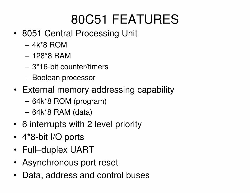
80C51 FEATURES• 8051 Central Processing Unit
– 4k*8 ROM
– 128*8 RAM
– 3*16-bit counter/timers
– Boolean processor
• External memory addressing capability
– 64k*8 ROM (program)
– 64k*8 RAM (data)
• 6 interrupts with 2 level priority
• 4*8-bit I/O ports
• Full–duplex UART
• Asynchronous port reset
• Data, address and control buses

BLOCK DIAGRAM

LOGIC SYMBOL AND PIN DESCRIPTION
• VSS, Input, Ground: 0 V reference
• VCC, I, Power Supply: Power supply voltage
• P0.0–0.7, I/O, Port 0: Can have the function of 8-bit open-drain bidirectional port with Schmitt trigger inputs. Pins that have 1s written to them are floating and can be used as high-impedance inputs. Can have the function of multiplexed low-order address and data bus during accesses to external program and data memory using internal pull-ups.
• P1.0–P1.7, I/O, Port 1: Can have the function of 8-bit bidirectional port with internal pull-ups and Schmitt trigger inputs. Pins that have 1s written to them are pulled high by the internal pull-ups and can be used as inputs. Also, two pins can have alternate functions. T2, I/O, (P1.0): Timer/Counter 2. T2EX, I, (P1.1): Timer/Counter 2 with capture function.

• P2.0–P2.7, I/O, Port 2: Can have the function of 8-bit bidirectional port with internal pull-ups and Schmitt trigger inputs. Pins that have 1s written to them are pulled high by the internal pull-up resistors and can be used as inputs. As alternate function, generates the high-order address byte during accesses to external program and data memory.
• P3.0–P3.7, I/O, Port 3: Can have the function of 8-bit bidirectional port with internal pull-ups and Schmitt trigger inputs. Port 3 pins that have 1s written to them are pulled high by the internal pull-ups and can be used as inputs. Also, each pin can have alternate function. RxD, I, (P3.0):Serial input port. TxD, O, (P3.1):Serial output port. INT0\, I, (P3.2):External interrupt. INT1\, I, (P3.3):External interrupt. T0, I, (P3.4): Timer 0 external input. T1, I, (P3.5): Timer 1 external input. WR\, O, (P3.6):External data memory write strobe. RD\, O, (P3.7): External data memory read strobe

• RST, I, Reset: A high on this pin resets the microcontroller.
• ALE/PROG\, I/O, Address Latch Enable/Program Pulse:ALE output pulse is used for latching the low byte of the address during an access to external memory. PROG pin is the program pulse input during EPROM programming.
• PSEN, O, Program Store Enable: External program memory read strobe.

• EA\ / VPP, I, External Access Enable/Programming Supply Voltage: If EA\ is externally held low, the microcontroller executes the entire code from external program memory. If EA\ is externally held high, the microcontroller executes the code located at memory locations 0000H to 0FFFH from the internal ROM. VPPpin receives the programming supply voltage during EPROM programming.
• XTAL1, I, Crystal 1: Input to the inverting oscillator amplifier and clock generator circuit.
• XTAL2, O, Crystal 2: Output from the inverting oscillator amplifier.

Port 0 layout
If CONTROL=0, P0 is an open-drain bidirectional port. The output of the NAND gate is 1, so, the Mp transistor is in cut-off stage, determining the open-drain configuration of the port. So, if the port is used for output, external pull-ups are used. If the port is used as an input port, logical value 1 is software set to the pin, so, the Mntransistor is in cut-off stage and the input floats.
If CONTROL=1, P0 is used for address and data bus using internal pull-ups. The output of the NAND gate isn’t influenced by the CONTROL signal, so, the state of the Mp transistor is determined only by the logical state of the address or data transmitted.

EXTERNAL PROGRAM MEMORY READ CYCLE
AND CONFIGURATION
• Address is transmitted first through P0 and P2 ports on the address bus. Because P0 port changes its function becoming data port, A0-A7 is latched when the ALE signal becomes active. PSEN\ signal becomes active and the information in the program memory is transmitted on the data bus being received through P0 port.

EXTERNAL DATA MEMORY READ AND WRITE CYCLES
• For the read cycle, address is transmitted first through P0 and P2 ports on the address bus. Because P0 port changes its function becoming data port, A0-A7 is latched when the ALE signal becomes active. RD\ signal becomes active and the information in the data memory is transmitted on the data bus being received through P0 port.
• For the write, cycle address is transmitted first through P0 and P2 ports on the address bus. Because P0 port changes its function becoming data port, A0-A7 is latched when the ALE signal becomes active. Data is transmitted through P0 port on the data bus and when WR\ signal becomes active is stored in the data memory.
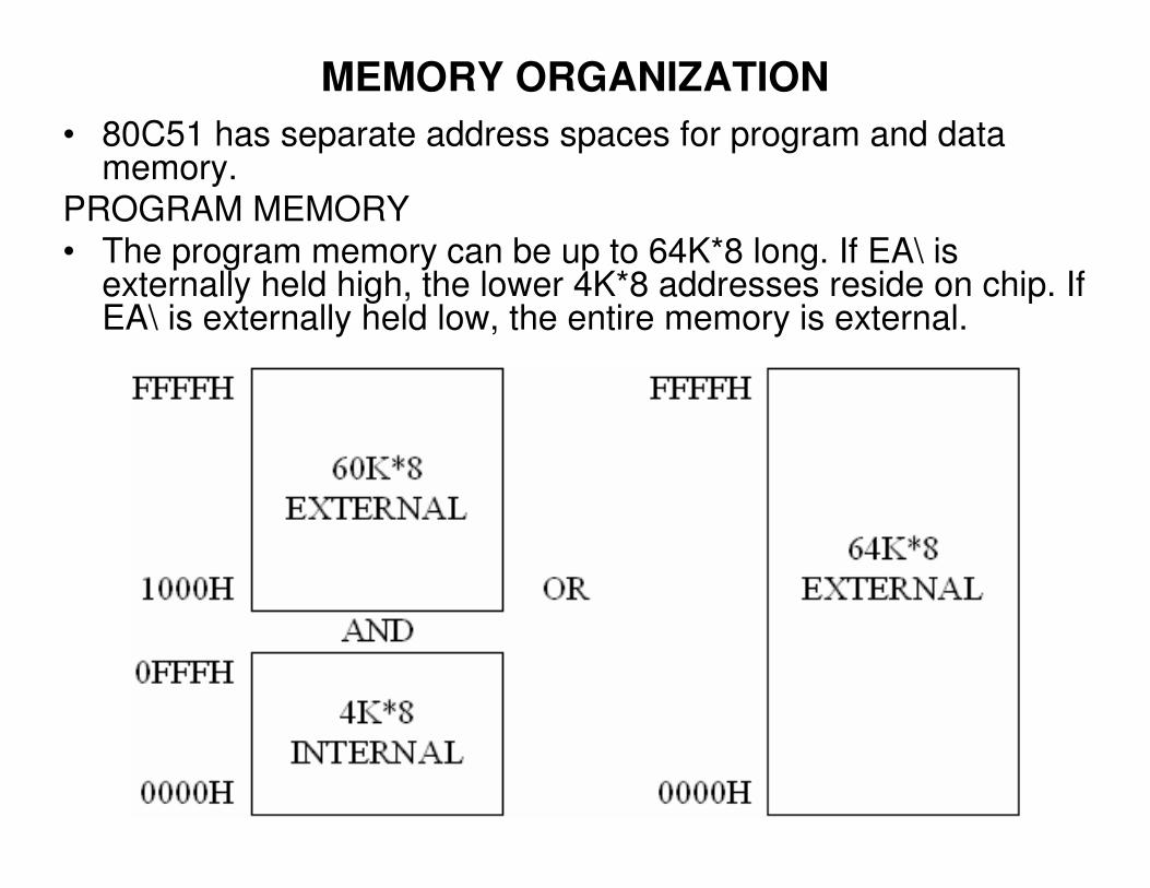
MEMORY ORGANIZATION
• 80C51 has separate address spaces for program and data memory.
PROGRAM MEMORY
• The program memory can be up to 64K*8 long. If EA\ is externally held high, the lower 4K*8 addresses reside on chip. If EA\ is externally held low, the entire memory is external.

DATA MEMORY• 80C51 has 128*8 internal RAM plus a number of Special
Function Registers (SFRs). The lower 128*8 RAM addresses can be accessed either by direct or indirect addressing. SFRscan be accessed only by direct addressing. Direct addressing specifies the address through a number, indirect addressing specifies the address through a register.
• External data memory can be up to 64K*8 long.

DIRECT AND INDIRECT ADDRESS AREA
• The lower 128*8 addresses can be divided into 3 segments:
• Register Banks 0-3:
00H through 1FH (32
bytes). The microcontroller after
reset default to register
bank 0. Register bank
selection is done by
software. Each register bank contains 8 one-
byte registers, 0
through 7.
• Bit Addressable Area: 20H through 2FH (16 bytes). Each one of the
128 bits can be directly addressed (00H through 7FH). Each of the 16
bytes can be addressed as a byte.
• Scratch Pad Area: 30H through 7FH (80 bytes). Used for data RAM.

SPECIAL
FUNCTION REGISTERS
• The SFRs marked with * are both bit
and byte addressable
• The other are only
byte addressable.
• After reset, each
SFR is loaded with a value that
doesn’t interfere with possible user
values.

SFR MEMORY MAP
• Byte and bit addressable SFRs are located on the first column.

Interrupts System• When an interrupt occurs, the microcontroller
suspends temporarly the program execution and starts running the specific interrupt routine
• For execution of interrupt routine the following steps are needed:– Save on stack the address of the next program instruction (2
octets) and of the PSW (2 octets).– Determine source of interrupt (interrupr number). Any
interrupt source has an interrupt vector, keeping the jump instruction at the address when starts the interrupt routine. Vector address is calculated by microcontroller. Interrupt vectors (8 octets) are stored into a specific table.
– Accesses the interrupt vector table and finds the routine address.
– Executes the interrupr routine.– Interrupt routine ends with IRET instruction, loading from
stack the location of the next program instruction (2 octets) and PSW (2 octets)

• Interrupts implementation :– Bit EA from register IE set to 1; means interrupts enabling
– Set to 1 all bits in register IE for interrupts will be used
– Each interrupt vector will be loaded with a long jumplong jumpinstruction to the address of the interrupt routine
– For external interrupts, pins INT0\ (P3.2) and INT1\ (P3.3) must be set to 1, and corresponding bits (IT0 şi IT1) from TCON register must be set or reset for activating interrupts on level or edge basis.
• 80C51 microcontroller interrupts

IE Register structure
• Bit or byte addressable. If EA is 0, all interrupts are disabled. If EA is 1, any interrupt is enabled by setting its bit to 1.
• Bit functions:– EA, IE.7: if EA=0, neither interrupt will be acknowledged. If
EA=1, each interrupt source may be individually enabled or disabled.
– ET2, IE.5: timer 2 overflow
– ES, IE.4: interrupt serial port
– ET1, IE.3: Timer 1 overflow
– EX1, IE.2: external interrupt 1
– ET0, IE.1: Timer 0 overflow
– EX0, IE.0: external interrupt 0

Interrupts priorities• Two priority levels. The higher one may interrupt the other. For priority
assignement corresponding bit from IP register must be set to 1 or 0.
• Priorities from high to low are: IE0, TF0, IE1, TF1, RI or TI and TF2 or EXF2.
IP register
• Bit or byte addressable.
Bit functions:
– PT2, IP.5: Timer 2 interrupt priority level (only 8052)
– PS, IP.4: serial port priority level
– PT1, IP.3: Timer 1 interrupt priority level
– PX1,IP.2: external interrupt 1 priority level
– PT0, IP.1: Timer 0 interrupt priority level
– PX0, IP.0: external interrupt 0 priority level

Registry of the Timer SystemTCON register
• Bit or byte addressable. Bit functions:– TF1, TCON.7: Flag Timer 1 overflow. Hardware erased when interrupt
routine is running
– TR1, TCON.6: Timer 1 control bit. if TR1=1, Timer 1 ON. if TR1=0, Timer 1 OFF.
– TF0, TCON.5: Flag Timer 0 overflow. Same as Flag Timer 1 overflow.
– TR0, TCON.4: Timer 0 control bit.Same as for Timer 1.
– IE1, TCON.3: Flag for external interrupt 1. Set hardware when externalinterrupt 1 edge detected; hardware reset when processing interrupt.
– IT1, TCON.2: Interrupt 1 type control bit. If IT1=1, interrupt 1 is triggeredby a falling down edge. If IT1=0, interrupt 1 is triggered by level 0.
– IE0, TCON.1: Flag for external interrupt 0. Set hardware when interruptedge detected, hardware erased when interrupt processing.
– IT0, TCON.0: Interrupt 0 type control bit . If IT0=1, interrupt 0 is triggeredby falling edge. If IT0=0, interrupt 0 is treiggered by logic level 0.

TMOD Register• Byte addressable. Bit functiones:• GATE: If GATE=1, TIMERx will run if TRx=1 and INTx=1 (hardware control).
If GATE=0, TIMERx will run as TRx=1 (software control).• C/T\, Timer or Counter Selector. If C/T\=0, Timer operation (input from
internal clock). If C/T\=1, Counter operation (input from Tx).• M1, M0: operation mode selection

Serial Communication
SCON Register• Bit or byte addressable. Bit functions:
– SM0: Bit 0 Serial Port mode (MSB).– SM1: Bit 1 Serial Port mode(LSB).
– SM2: Activates communications modes
– REN: Software set or reset for Reception enable/disable– TB8, RB8: Special role in operation modes 2 and 3
– TI: Transmission interrupt– RI: Reception interrupt

mode 0: port communicates with fixed baud rate
• Baud rate = Osc Freq/12
• Port acts as a 8bit shift register; data sent with LSB first through RXD pin.
mode 1: variable baud rate, generated by Timer 1
• Baud rate = (K * Osc Freq)/32 * 12 * [256 -(TH1)]
• Bit SMOD from PCON register determines K value. If SMOD = 0, K = 1, if SMOD = 1, K = 2.
• TH1 = 256 – (K * Osc Freq) / (384 * Baud Rate)
• Frame format: 1 start bit, 8 data bit, 1 stop bit.
• Interrupts TI şi RI are activated when a framewas sent or received
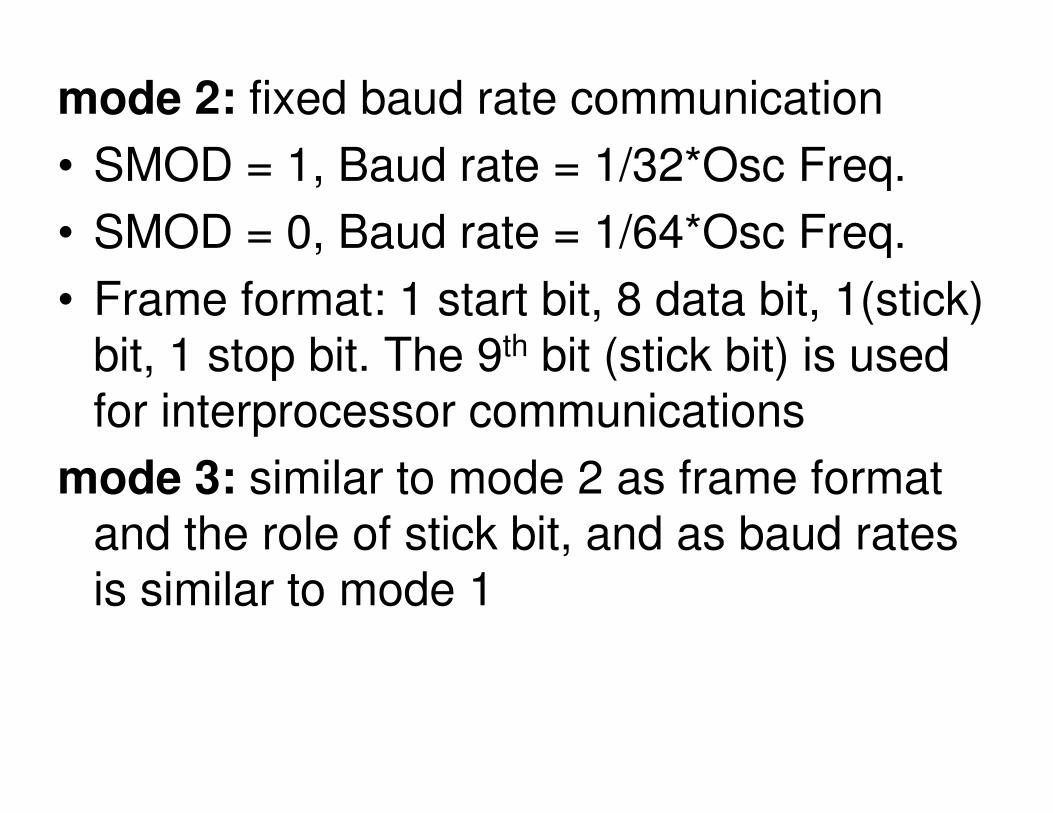
mode 2: fixed baud rate communication
• SMOD = 1, Baud rate = 1/32*Osc Freq.
• SMOD = 0, Baud rate = 1/64*Osc Freq.
• Frame format: 1 start bit, 8 data bit, 1(stick) bit, 1 stop bit. The 9th bit (stick bit) is usedfor interprocessor communications
mode 3: similar to mode 2 as frame format and the role of stick bit, and as baud rates is similar to mode 1

Proposed Problems
• Design a system based on a 80C51 microcontroller, with the following blocks:
– quartz oscillator with a 12MHz frequency
– Reset circuit
– 8k*8 bit external program memory with the low
(base) address 0000H
– 8k*8 bit data & program external memory with low
address of 2000H
– 8k*8 bit external data memory with the base
address 4000H

74HCT08
1
23
C2
33p
VCC
109876543
252421232
20221
1112131516171819
A0A1A2A3A4A5A6A7A8A9A10A11A12
CEOEWR
O0O1O2O3O4O5O6O7
0
0
74HCT373
1113478
13141718
256912151619
OCC1D2D3D4D5D6D7D8D
1Q2Q3Q4Q5Q6Q7Q8Q
0
10u
74HCT10
1122
13
12MHz
R28k2
S180C51
2930
40
31
1918
9
3938373635343332
12345678
2122232425262728
1011121314151617
PSENALE
VCC
EA
X1X2
RST
P0.0/AD0P0.1/AD1P0.2/AD2P0.3/AD3P0.4/AD4P0.5/AD5P0.6/AD6P0.7/AD7
P1.0/T2P1.1/T2EXP1.2/ECIP1.3/CEX0P1.4/CEX1P1.5/CEX2P1.6/CEX3P1.7/CEX4
P2.0/A8P2.1/A9
P2.2/A10P2.3/A11P2.4/A12P2.5/A13P2.6/A14P2.7/A15
P3.0/RXDP3.1/TXD
P3.2/INT0P3.3/INT1
P3.4/T0P3.5/T1
P3.6/WRP3.7/RD
0
109876543
252421232
20221
1112131516171819
A0A1A2A3A4A5A6A7A8A9A10A11A12
CEOEVPP
O0O1O2O3O4O5O6O7
VPP
R1
220
C1
33p
109876543
252421232
20221
1112131516171819
A0A1A2A3A4A5A6A7A8A9A10A11A12
CEOEWR
O0O1O2O3O4O5O6O7
0
0
VCC
74HCT138
15141312111097
1
5
23
64
Y0Y1Y2Y3Y4Y5Y6Y7
A
G2B
BC
G1G2A

• Design a system based on a 80C51 microcontroller, with the following blocks:
– quartz oscillator with a 12MHz frequency
– Reset circuit
– 8k*8 bit external program memory with the low
(base) address 0000H
– Output port at address 011XXXXXXXXXXXXXb
– Input port at address 111XXXXXXXXXXXXXb ,
here having connected two keys

0
10u
74HCT02
2
31
12MHz
74HCT138
15141312111097
1
5
23
64
Y0Y1Y2Y3Y4Y5Y6Y7
A
G2B
BC
G1G2A
0
S3
74HCT374
1
347813141718
2569
12151619
11OC
1D2D3D4D5D6D7D8D
1Q2Q3Q4Q5Q6Q7Q8Q
CLK
109876543
252421232
20221
1112131516171819
A0A1A2A3A4A5A6A7A8A9A10A11A12
CEOEVPP
O0O1O2O3O4O5O6O7
0
74HCT244
12468
1911131517
18161412
9753
1G1A11A21A31A4
2G2A12A22A32A4
1Y11Y21Y31Y4
2Y12Y22Y32Y4
0
S1
VPP
R28k2
C1
33p
R4
10k
0
0
0
C2
33p
80C51
2930
40
31
1918
9
3938373635343332
12345678
2122232425262728
1011121314151617
PSENALE
VCC
EA
X1X2
RST
P0.0/AD0P0.1/AD1P0.2/AD2P0.3/AD3P0.4/AD4P0.5/AD5P0.6/AD6P0.7/AD7
P1.0/T2P1.1/T2EXP1.2/ECIP1.3/CEX0P1.4/CEX1P1.5/CEX2P1.6/CEX3P1.7/CEX4
P2.0/A8P2.1/A9
P2.2/A10P2.3/A11P2.4/A12P2.5/A13P2.6/A14P2.7/A15
P3.0/RXDP3.1/TXD
P3.2/INT0P3.3/INT1
P3.4/T0P3.5/T1
P3.6/WRP3.7/RD
R3
10k
74HCT373
111
3478
13141718
256912151619
OCC1D2D3D4D5D6D7D8D
1Q2Q3Q4Q5Q6Q7Q8Q
R1
220
0
74HCT32
1
23
74HCT10
1122
13
VCC
0
VCC
VCC
S2

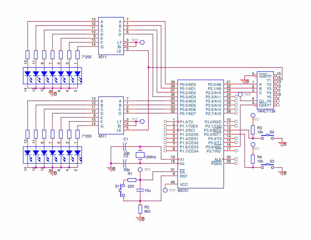
• Design a system based on a 80C51 microcontroller, with the following blocks:
– quartz oscillator with a 12MHz frequency
– Reset circuit
– Output port at address XXXXX001XXXXXXXXb having connected two 7-segments LED displays using common
cathode, with: VLED=1,7V and ILED=10mA
– 2 keys connected at interrupt input lines
– Only internal program memory is used
Hint: Calculus for resistor values (for the LED based display) is
given by::
R=(VOHTYP-VLED)/ILED=(4,25V-1,7V)/10mA=255Ω
VCC
74HCT138
15141312111097
1
5
23
64
Y0Y1Y2Y3Y4Y5Y6Y7
A
G2B
BC
G1G2A
S3R410k
7*255
VCC
00
VCC
S1
R1
220
12
346
5
810
12
7911
13
14
VCC
12MHz
12
346
5
810
12
7911
13
14
0
S2R310k
10u
C1
33pC2
33p
0
7*255
4511
7126
345
131211109
1514
ABCD
LTBILE
ABCDEFG
VCC
R28k2
0
VCC
80C51
2930
40
31
1918
9
3938373635343332
12345678
2122232425262728
1011121314151617
PSENALE
VCC
EA
X1X2
RST
P0.0/AD0P0.1/AD1P0.2/AD2P0.3/AD3P0.4/AD4P0.5/AD5P0.6/AD6P0.7/AD7
P1.0/T2P1.1/T2EXP1.2/ECIP1.3/CEX0P1.4/CEX1P1.5/CEX2P1.6/CEX3P1.7/CEX4
P2.0/A8P2.1/A9
P2.2/A10P2.3/A11P2.4/A12P2.5/A13P2.6/A14P2.7/A15
P3.0/RXDP3.1/TXD
P3.2/INT0P3.3/INT1
P3.4/T0P3.5/T1
P3.6/WRP3.7/RD
0
4511
7126
345
131211109
1514
ABCD
LTBILE
ABCDEFG
0
VCC