Arithmetic and Logic Instructions in Microprocessor 8086/8088
August 1990 Order Number: 231456-006
80888-BIT HMOS MICROPROCESSOR
8088/8088-2
Y 8-Bit Data Bus Interface
Y 16-Bit Internal Architecture
Y Direct Addressing Capability to 1 Mbyteof Memory
Y Direct Software Compatibility with 8086CPU
Y 14-Word by 16-Bit Register Set withSymmetrical Operations
Y 24 Operand Addressing Modes
Y Byte, Word, and Block Operations
Y 8-Bit and 16-Bit Signed and UnsignedArithmetic in Binary or Decimal,Including Multiply and Divide
Y Two Clock Rates:Ð 5 MHz for 8088Ð 8 MHz for 8088-2
Y Available in EXPRESSÐ Standard Temperature RangeÐ Extended Temperature Range
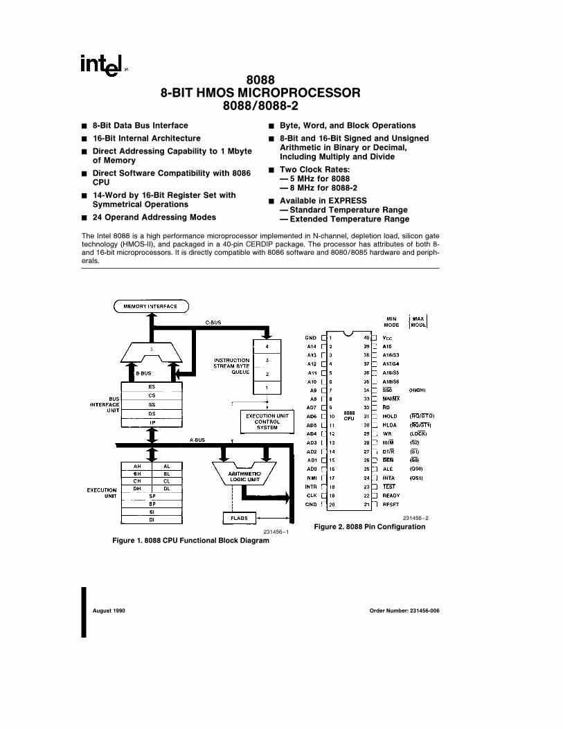
The Intel 8088 is a high performance microprocessor implemented in N-channel, depletion load, silicon gatetechnology (HMOS-II), and packaged in a 40-pin CERDIP package. The processor has attributes of both 8-and 16-bit microprocessors. It is directly compatible with 8086 software and 8080/8085 hardware and periph-erals.
231456–1
Figure 1. 8088 CPU Functional Block Diagram
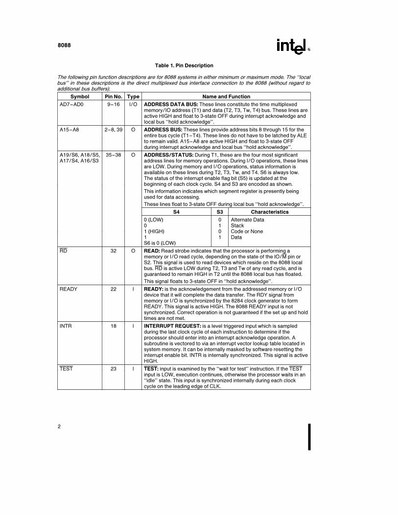
231456–2
Figure 2. 8088 Pin Configuration
8088
Table 1. Pin Description
The following pin function descriptions are for 8088 systems in either minimum or maximum mode. The ‘‘localbus’’ in these descriptions is the direct multiplexed bus interface connection to the 8088 (without regard toadditional bus buffers).
Symbol Pin No. Type Name and Function
AD7–AD0 9–16 I/O ADDRESS DATA BUS: These lines constitute the time multiplexedmemory/IO address (T1) and data (T2, T3, Tw, T4) bus. These lines areactive HIGH and float to 3-state OFF during interrupt acknowledge andlocal bus ‘‘hold acknowledge’’.
A15–A8 2–8, 39 O ADDRESS BUS: These lines provide address bits 8 through 15 for theentire bus cycle (T1–T4). These lines do not have to be latched by ALEto remain valid. A15–A8 are active HIGH and float to 3-state OFFduring interrupt acknowledge and local bus ‘‘hold acknowledge’’.
A17/S4, A16/S3A19/S6, A18/S5, 35–38 O ADDRESS/STATUS: During T1, these are the four most significant
address lines for memory operations. During I/O operations, these linesare LOW. During memory and I/O operations, status information isavailable on these lines during T2, T3, Tw, and T4. S6 is always low.The status of the interrupt enable flag bit (S5) is updated at thebeginning of each clock cycle. S4 and S3 are encoded as shown.
This information indicates which segment register is presently beingused for data accessing.
These lines float to 3-state OFF during local bus ‘‘hold acknowledge’’.
S4 S3 Characteristics
0 (LOW) 0 Alternate Data0 1 Stack1 (HIGH) 0 Code or None1 1 DataS6 is 0 (LOW)
RD 32 O READ: Read strobe indicates that the processor is performing amemory or I/O read cycle, depending on the state of the IO/M pin orS2. This signal is used to read devices which reside on the 8088 localbus. RD is active LOW during T2, T3 and Tw of any read cycle, and isguaranteed to remain HIGH in T2 until the 8088 local bus has floated.
This signal floats to 3-state OFF in ‘‘hold acknowledge’’.
READY 22 I READY: is the acknowledgement from the addressed memory or I/Odevice that it will complete the data transfer. The RDY signal frommemory or I/O is synchronized by the 8284 clock generator to formREADY. This signal is active HIGH. The 8088 READY input is notsynchronized. Correct operation is not guaranteed if the set up and holdtimes are not met.
INTR 18 I INTERRUPT REQUEST: is a level triggered input which is sampledduring the last clock cycle of each instruction to determine if theprocessor should enter into an interrupt acknowledge operation. Asubroutine is vectored to via an interrupt vector lookup table located insystem memory. It can be internally masked by software resetting theinterrupt enable bit. INTR is internally synchronized. This signal is activeHIGH.
TEST 23 I TEST: input is examined by the ‘‘wait for test’’ instruction. If the TESTinput is LOW, execution continues, otherwise the processor waits in an‘‘idle’’ state. This input is synchronized internally during each clockcycle on the leading edge of CLK.
2
8088
Table 1. Pin Description (Continued)
Symbol Pin No. Type Name and Function
NMI 17 I NON-MASKABLE INTERRUPT: is an edge triggered input which causes atype 2 interrupt. A subroutine is vectored to via an interrupt vector lookuptable located in system memory. NMI is not maskable internally bysoftware. A transition from a LOW to HIGH initiates the interrupt at the endof the current instruction. This input is internally synchronized.
RESET 21 I RESET: causes the processor to immediately terminate its present activity.The signal must be active HIGH for at least four clock cycles. It restartsexecution, as described in the instruction set description, when RESETreturns LOW. RESET is internally synchronized.
CLK 19 I CLOCK: provides the basic timing for the processor and bus controller. It isasymmetric with a 33% duty cycle to provide optimized internal timing.
VCC 40 VCC: is the a5V g10% power supply pin.
GND 1, 20 GND: are the ground pins.
MN/MX 33 I MINIMUM/MAXIMUM: indicates what mode the processor is to operate in.The two modes are discussed in the following sections.
The following pin function descriptions are for the 8088 minimum mode (i.e., MN/MX e VCC). Only the pinfunctions which are unique to minimum mode are described; all other pin functions are as described above.
Symbol Pin No. Type Name and Function
IO/M 28 O STATUS LINE: is an inverted maximum mode S2. It is used to distinguish amemory access from an I/O access. IO/M becomes valid in the T4 preceding abus cycle and remains valid until the final T4 of the cycle (I/O e HIGH, M e
LOW). IO/M floats to 3-state OFF in local bus ‘‘hold acknowledge’’.
WR 29 O WRITE: strobe indicates that the processor is performing a write memory or writeI/O cycle, depending on the state of the IO/M signal. WR is active for T2, T3, andTw of any write cycle. It is active LOW, and floats to 3-state OFF in local bus‘‘hold acknowledge’’.
INTA 24 O INTA: is used as a read strobe for interrupt acknowledge cycles. It is active LOWduring T2, T3, and Tw of each interrupt acknowledge cycle.
ALE 25 O ADDRESS LATCH ENABLE: is provided by the processor to latch the addressinto an address latch. It is a HIGH pulse active during clock low of T1 of any buscycle. Note that ALE is never floated.
DT/R 27 O DATA TRANSMIT/RECEIVE: is needed in a minimum system that desires to usea data bus transceiver. It is used to control the direction of data flow through thetransceiver. Logically, DT/R is equivalent to S1 in the maximum mode, and itstiming is the same as for IO/M (T e HIGH, R e LOW). This signal floats to3-state OFF in local ‘‘hold acknowledge’’.
DEN 26 O DATA ENABLE: is provided as an output enable for the data bus transceiver in aminimum system which uses the transceiver. DEN is active LOW during eachmemory and I/O access, and for INTA cycles. For a read or INTA cycle, it isactive from the middle of T2 until the middle of T4, while for a write cycle, it isactive from the beginning of T2 until the middle of T4. DEN floats to 3-state OFFduring local bus ‘‘hold acknowledge’’.
3
8088
Table 1. Pin Description (Continued)
Symbol Pin No. Type Name and Function
HOLD,HLDA
31, 30 I, O HOLD: indicates that another master is requesting a local bus ‘‘hold’’. To beacknowledged, HOLD must be active HIGH. The processor receiving the ‘‘hold’’request will issue HLDA (HIGH) as an acknowledgement, in the middle of a T4 orTi clock cycle. Simultaneous with the issuance of HLDA the processor will floatthe local bus and control lines. After HOLD is detected as being LOW, theprocessor lowers HLDA, and when the processor needs to run another cycle, itwill again drive the local bus and control lines. HOLD and HLDA have internalpull-up resistors.
Hold is not an asynchronous input. External synchronization should be provided ifthe system cannot otherwise guarantee the set up time.
SSO 34 O STATUS LINE: is logically equivalent to SO in the maximum mode. Thecombination of SSO, IO/M and DT/R allows the system to completely decode thecurrent bus cycle status.
IO/M DT/R SSO Characteristics
1(HIGH) 0 0 Interrupt Acknowledge1 0 1 Read I/O Port1 1 0 Write I/O Port1 1 1 Halt0(LOW) 0 0 Code Access0 0 1 Read Memory0 1 0 Write Memory0 1 1 Passive
The following pin function descriptions are for the 8088/8288 system in maximum mode (i.e., MN/MX e
GND). Only the pin functions which are unique to maximum mode are described; all other pin functions are asdescribed above.
Symbol Pin No. Type Name and Function
S2, S1, S0 26–28 O STATUS: is active during clock high of T4, T1, and T2, and is returned to thepassive state (1,1,1) during T3 or during Tw when READY is HIGH. This status isused by the 8288 bus controller to generate all memory and I/O access controlsignals. Any change by S2, S1, or S0 during T4 is used to indicate the beginningof a bus cycle, and the return to the passive state in T3 and Tw is used toindicate the end of a bus cycle.These signals float to 3-state OFF during ‘‘hold acknowledge’’. During the firstclock cycle after RESET becomes active, these signals are active HIGH. Afterthis first clock, they float to 3-state OFF.
S2 S1 S0 Characteristics
0(LOW) 0 0 Interrupt Acknowledge0 0 1 Read I/O Port0 1 0 Write I/O Port0 1 1 Halt1(HIGH) 0 0 Code Access1 0 1 Read Memory1 1 0 Write Memory1 1 1 Passive
4
8088
Table 1. Pin Description (Continued)
Symbol Pin No. Type Name and Function
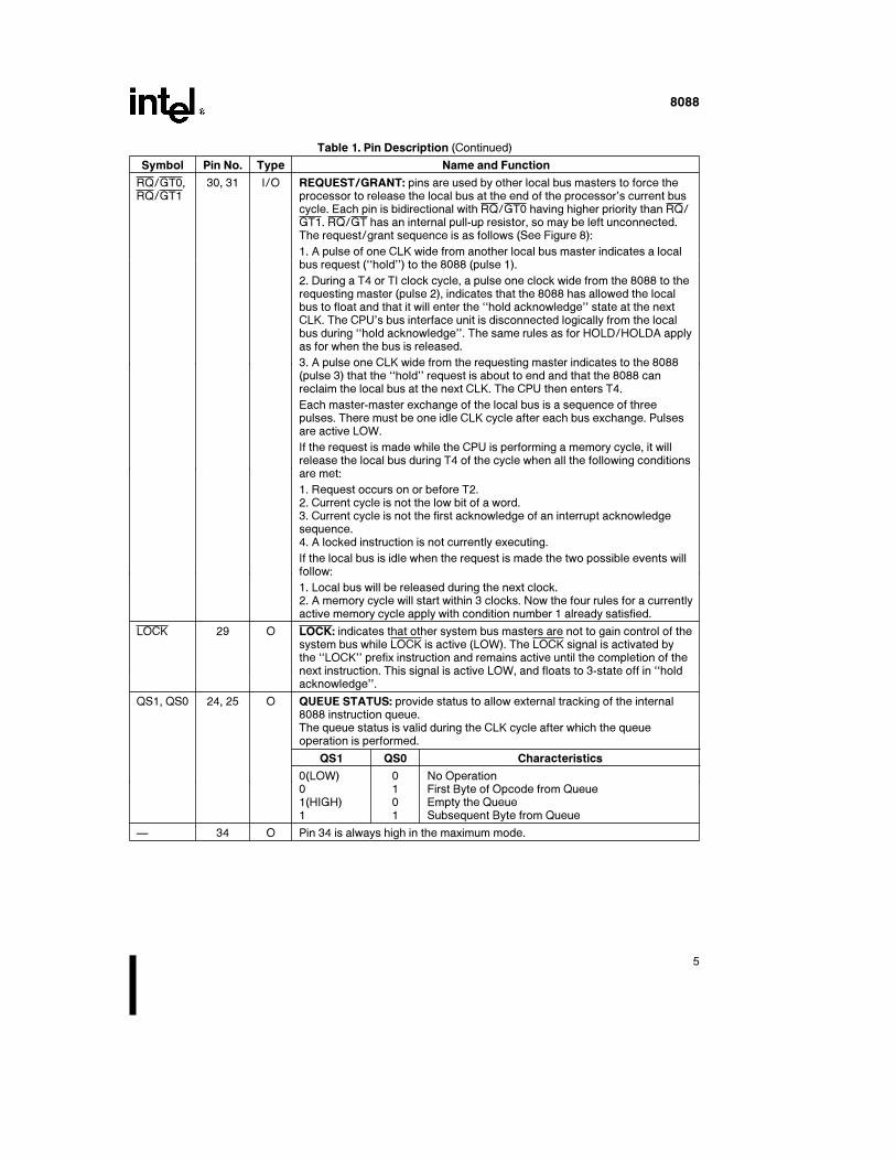
RQ/GT0,RQ/GT1
30, 31 I/O REQUEST/GRANT: pins are used by other local bus masters to force theprocessor to release the local bus at the end of the processor’s current buscycle. Each pin is bidirectional with RQ/GT0 having higher priority than RQ/GT1. RQ/GT has an internal pull-up resistor, so may be left unconnected.The request/grant sequence is as follows (See Figure 8):
1. A pulse of one CLK wide from another local bus master indicates a localbus request (‘‘hold’’) to the 8088 (pulse 1).
2. During a T4 or TI clock cycle, a pulse one clock wide from the 8088 to therequesting master (pulse 2), indicates that the 8088 has allowed the localbus to float and that it will enter the ‘‘hold acknowledge’’ state at the nextCLK. The CPU’s bus interface unit is disconnected logically from the localbus during ‘‘hold acknowledge’’. The same rules as for HOLD/HOLDA applyas for when the bus is released.
3. A pulse one CLK wide from the requesting master indicates to the 8088(pulse 3) that the ‘‘hold’’ request is about to end and that the 8088 canreclaim the local bus at the next CLK. The CPU then enters T4.
Each master-master exchange of the local bus is a sequence of threepulses. There must be one idle CLK cycle after each bus exchange. Pulsesare active LOW.
If the request is made while the CPU is performing a memory cycle, it willrelease the local bus during T4 of the cycle when all the following conditionsare met:
1. Request occurs on or before T2.2. Current cycle is not the low bit of a word.3. Current cycle is not the first acknowledge of an interrupt acknowledgesequence.4. A locked instruction is not currently executing.
If the local bus is idle when the request is made the two possible events willfollow:
1. Local bus will be released during the next clock.2. A memory cycle will start within 3 clocks. Now the four rules for a currentlyactive memory cycle apply with condition number 1 already satisfied.
LOCK 29 O LOCK: indicates that other system bus masters are not to gain control of thesystem bus while LOCK is active (LOW). The LOCK signal is activated bythe ‘‘LOCK’’ prefix instruction and remains active until the completion of thenext instruction. This signal is active LOW, and floats to 3-state off in ‘‘holdacknowledge’’.
QS1, QS0 24, 25 O QUEUE STATUS: provide status to allow external tracking of the internal8088 instruction queue.The queue status is valid during the CLK cycle after which the queueoperation is performed.
QS1 QS0 Characteristics
0(LOW) 0 No Operation0 1 First Byte of Opcode from Queue1(HIGH) 0 Empty the Queue1 1 Subsequent Byte from Queue
Ð 34 O Pin 34 is always high in the maximum mode.
5
8088
231456–3
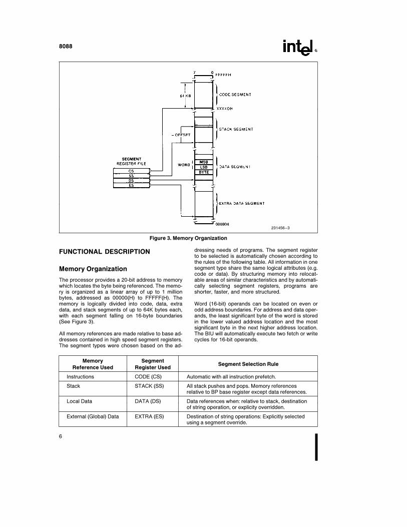
Figure 3. Memory Organization
FUNCTIONAL DESCRIPTION
Memory Organization
The processor provides a 20-bit address to memorywhich locates the byte being referenced. The memo-ry is organized as a linear array of up to 1 millionbytes, addressed as 00000(H) to FFFFF(H). Thememory is logically divided into code, data, extradata, and stack segments of up to 64K bytes each,with each segment falling on 16-byte boundaries(See Figure 3).
All memory references are made relative to base ad-dresses contained in high speed segment registers.The segment types were chosen based on the ad-
dressing needs of programs. The segment registerto be selected is automatically chosen according tothe rules of the following table. All information in onesegment type share the same logical attributes (e.g.code or data). By structuring memory into relocat-able areas of similar characteristics and by automati-cally selecting segment registers, programs areshorter, faster, and more structured.
Word (16-bit) operands can be located on even orodd address boundaries. For address and data oper-ands, the least significant byte of the word is storedin the lower valued address location and the mostsignificant byte in the next higher address location.The BIU will automatically execute two fetch or writecycles for 16-bit operands.
Memory SegmentSegment Selection Rule
Reference Used Register Used
Instructions CODE (CS) Automatic with all instruction prefetch.
Stack STACK (SS) All stack pushes and pops. Memory referencesrelative to BP base register except data references.
Local Data DATA (DS) Data references when: relative to stack, destinationof string operation, or explicity overridden.
External (Global) Data EXTRA (ES) Destination of string operations: Explicitly selectedusing a segment override.
6
8088
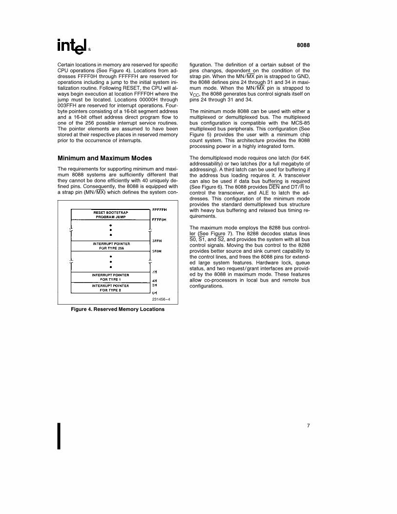
Certain locations in memory are reserved for specificCPU operations (See Figure 4). Locations from ad-dresses FFFF0H through FFFFFH are reserved foroperations including a jump to the initial system ini-tialization routine. Following RESET, the CPU will al-ways begin execution at location FFFF0H where thejump must be located. Locations 00000H through003FFH are reserved for interrupt operations. Four-byte pointers consisting of a 16-bit segment addressand a 16-bit offset address direct program flow toone of the 256 possible interrupt service routines.The pointer elements are assumed to have beenstored at their respective places in reserved memoryprior to the occurrence of interrupts.
Minimum and Maximum Modes
The requirements for supporting minimum and maxi-mum 8088 systems are sufficiently different thatthey cannot be done efficiently with 40 uniquely de-fined pins. Consequently, the 8088 is equipped witha strap pin (MN/MX) which defines the system con-
231456–4
Figure 4. Reserved Memory Locations
figuration. The definition of a certain subset of thepins changes, dependent on the condition of thestrap pin. When the MN/MX pin is strapped to GND,the 8088 defines pins 24 through 31 and 34 in maxi-mum mode. When the MN/MX pin is strapped toVCC, the 8088 generates bus control signals itself onpins 24 through 31 and 34.
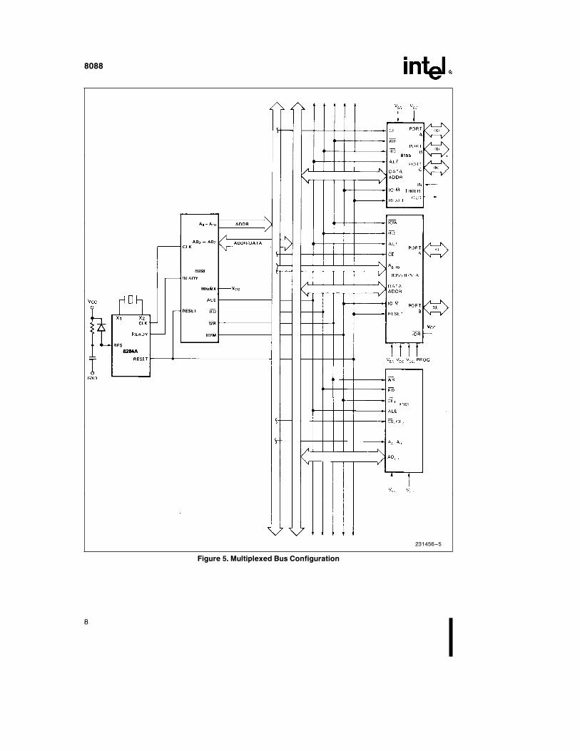
The minimum mode 8088 can be used with either amultiplexed or demultiplexed bus. The multiplexedbus configuration is compatible with the MCS-85multiplexed bus peripherals. This configuration (SeeFigure 5) provides the user with a minimum chipcount system. This architecture provides the 8088processing power in a highly integrated form.
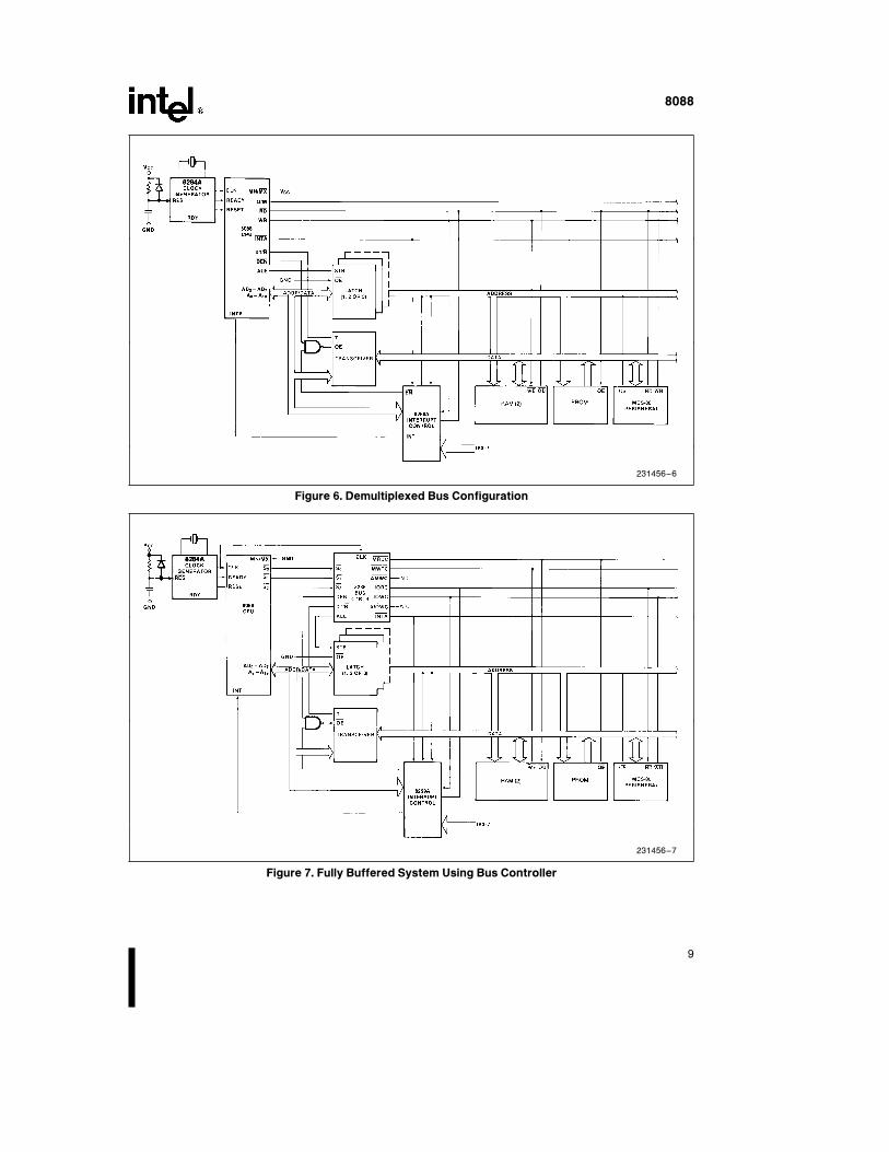
The demultiplexed mode requires one latch (for 64Kaddressability) or two latches (for a full megabyte ofaddressing). A third latch can be used for buffering ifthe address bus loading requires it. A transceivercan also be used if data bus buffering is required(See Figure 6). The 8088 provides DEN and DT/R tocontrol the transceiver, and ALE to latch the ad-dresses. This configuration of the minimum modeprovides the standard demultiplexed bus structurewith heavy bus buffering and relaxed bus timing re-quirements.
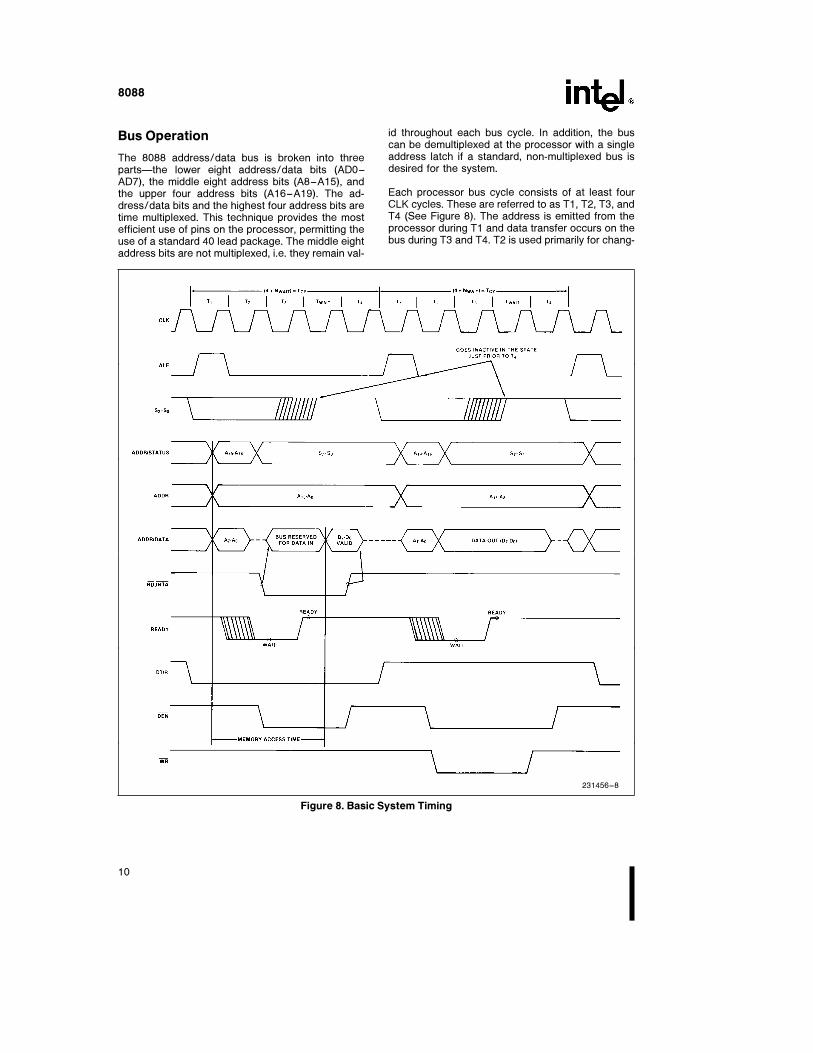
The maximum mode employs the 8288 bus control-ler (See Figure 7). The 8288 decodes status linesS0, S1, and S2, and provides the system with all buscontrol signals. Moving the bus control to the 8288provides better source and sink current capability tothe control lines, and frees the 8088 pins for extend-ed large system features. Hardware lock, queuestatus, and two request/grant interfaces are provid-ed by the 8088 in maximum mode. These featuresallow co-processors in local bus and remote busconfigurations.
7
8088
231456–5
Figure 5. Multiplexed Bus Configuration
8
8088
231456–6
Figure 6. Demultiplexed Bus Configuration
231456–7
Figure 7. Fully Buffered System Using Bus Controller
9
8088
Bus Operation
The 8088 address/data bus is broken into threepartsÐthe lower eight address/data bits (AD0–AD7), the middle eight address bits (A8–A15), andthe upper four address bits (A16–A19). The ad-dress/data bits and the highest four address bits aretime multiplexed. This technique provides the mostefficient use of pins on the processor, permitting theuse of a standard 40 lead package. The middle eightaddress bits are not multiplexed, i.e. they remain val-
id throughout each bus cycle. In addition, the buscan be demultiplexed at the processor with a singleaddress latch if a standard, non-multiplexed bus isdesired for the system.
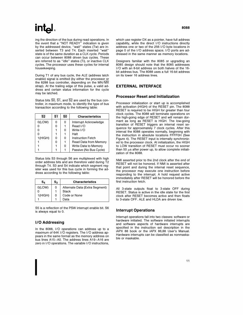
Each processor bus cycle consists of at least fourCLK cycles. These are referred to as T1, T2, T3, andT4 (See Figure 8). The address is emitted from theprocessor during T1 and data transfer occurs on thebus during T3 and T4. T2 is used primarily for chang-
231456–8
Figure 8. Basic System Timing
10
8088
ing the direction of the bus during read operations. Inthe event that a ‘‘NOT READY’’ indication is givenby the addressed device, ‘‘wait’’ states (Tw) are in-serted between T3 and T4. Each inserted ‘‘wait’’state is of the same duration as a CLK cycle. Periodscan occur between 8088 driven bus cycles. Theseare referred to as ‘‘idle’’ states (Ti), or inactive CLKcycles. The processor uses these cycles for internalhousekeeping.
During T1 of any bus cycle, the ALE (address latchenable) signal is emitted (by either the processor orthe 8288 bus controller, depending on the MN/MXstrap). At the trailing edge of this pulse, a valid ad-dress and certain status information for the cyclemay be latched.
Status bits S0, S1, and S2 are used by the bus con-troller, in maximum mode, to identify the type of bustransaction according to the following table:
S2 S1 S0 Characteristics
0(LOW) 0 0 Interrupt Acknowledge
0 0 1 Read I/O
0 1 0 Write I/O
0 1 1 Halt
1(HIGH) 0 0 Instruction Fetch
1 0 1 Read Data from Memory
1 1 0 Write Data to Memory
1 1 1 Passive (No Bus Cycle)
Status bits S3 through S6 are multiplexed with highorder address bits and are therefore valid during T2through T4. S3 and S4 indicate which segment reg-ister was used for this bus cycle in forming the ad-dress according to the following table:
S4 S3 Characteristics
0(LOW) 0 Alternate Data (Extra Segment)
0 1 Stack
1(HIGH) 0 Code or None
1 1 Data
S5 is a reflection of the PSW interrupt enable bit. S6is always equal to 0.
I/O Addressing
In the 8088, I/O operations can address up to amaximum of 64K I/O registers. The I/O address ap-pears in the same format as the memory address onbus lines A15–A0. The address lines A19–A16 arezero in I/O operations. The variable I/O instructions,
which use register DX as a pointer, have full addresscapability, while the direct I/O instructions directlyaddress one or two of the 256 I/O byte locations inpage 0 of the I/O address space. I/O ports are ad-dressed in the same manner as memory locations.
Designers familiar with the 8085 or upgrading an8085 design should note that the 8085 addressesI/O with an 8-bit address on both halves of the 16-bit address bus. The 8088 uses a full 16-bit addresson its lower 16 address lines.
EXTERNAL INTERFACE
Processor Reset and Initialization
Processor initialization or start up is accomplishedwith activation (HIGH) of the RESET pin. The 8088RESET is required to be HIGH for greater than fourclock cycles. The 8088 will terminate operations onthe high-going edge of RESET and will remain dor-mant as long as RESET is HIGH. The low-goingtransition of RESET triggers an internal reset se-quence for approximately 7 clock cycles. After thisinterval the 8088 operates normally, beginning withthe instruction in absolute locations FFFF0H (SeeFigure 4). The RESET input is internally synchroniz-ed to the processor clock. At initialization, the HIGHto LOW transition of RESET must occur no soonerthan 50 ms after power up, to allow complete initiali-zation of the 8088.
NMI asserted prior to the 2nd clock after the end ofRESET will not be honored. If NMI is asserted afterthat point and during the internal reset sequence,the processor may execute one instruction beforeresponding to the interrupt. A hold request activeimmediately after RESET will be honored before thefirst instruction fetch.
All 3-state outputs float to 3-state OFF duringRESET. Status is active in the idle state for the firstclock after RESET becomes active and then floatsto 3-state OFF. ALE and HLDA are driven low.
Interrupt Operations
Interrupt operations fall into two classes: software orhardware initiated. The software initiated interruptsand software aspects of hardware interrupts arespecified in the instruction set description in theiAPX 88 book or the iAPX 86,88 User’s Manual.Hardware interrupts can be classified as nonmaska-ble or maskable.
11
8088
Interrupts result in a transfer of control to a new pro-gram location. A 256 element table containing ad-dress pointers to the interrupt service program loca-tions resides in absolute locations 0 through 3FFH(See Figure 4), which are reserved for this purpose.Each element in the table is 4 bytes in size and cor-responds to an interrupt ‘‘type.’’ An interrupting de-vice supplies an 8-bit type number, during the inter-rupt acknowledge sequence, which is used to vectorthrough the appropriate element to the new interruptservice program location.
Non-Maskable Interrupt (NMI)
The processor provides a single non-maskable inter-rupt (NMI) pin which has higher priority than themaskable interrupt request (INTR) pin. A typical usewould be to activate a power failure routine. TheNMI is edge-triggered on a LOW to HIGH transition.The activation of this pin causes a type 2 interrupt.
NMI is required to have a duration in the HIGH stateof greater than two clock cycles, but is not requiredto be synchronized to the clock. Any higher goingtransition of NMI is latched on-chip and will be serv-iced at the end of the current instruction or betweenwhole moves (2 bytes in the case of word moves) ofa block type instruction. Worst case response toNMI would be for multiply, divide, and variable shiftinstructions. There is no specification on the occur-rence of the low-going edge; it may occur before,during, or after the servicing of NMI. Another high-going edge triggers another response if it occurs af-ter the start of the NMI procedure. The signal mustbe free of logical spikes in general and be free ofbounces on the low-going edge to avoid triggeringextraneous responses.
Maskable Interrupt (INTR)
The 8088 provides a single interrupt request input(INTR) which can be masked internally by softwarewith the resetting of the interrupt enable (IF) flag bit.The interrupt request signal is level triggered. It isinternally synchronized during each clock cycle onthe high-going edge of CLK. To be responded to,INTR must be present (HIGH) during the clock peri-od preceding the end of the current instruction or theend of a whole move for a block type instruction.During interrupt response sequence, further inter-rupts are disabled. The enable bit is reset as part ofthe response to any interrupt (INTR, NMI, softwareinterrupt, or single step), although the FLAGS regis-ter which is automatically pushed onto the stack re-flects the state of the processor prior to the inter-rupt. Until the old FLAGS register is restored, the
enable bit will be zero unless specifically set by aninstruction.
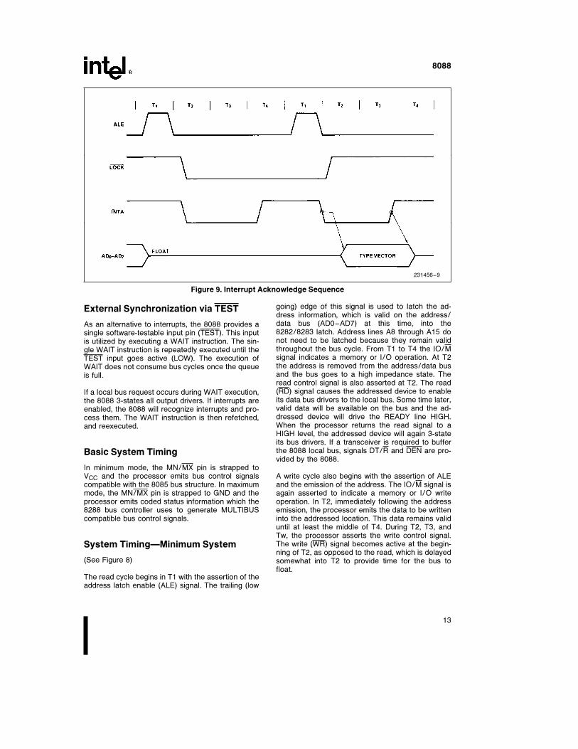
During the response sequence (See Figure 9), theprocessor executes two successive (back to back)interrupt acknowledge cycles. The 8088 emits theLOCK signal (maximum mode only) from T2 of thefirst bus cycle until T2 of the second. A local bus‘‘hold’’ request will not be honored until the end ofthe second bus cycle. In the second bus cycle, abyte is fetched from the external interrupt system(e.g., 8259A PIC) which identifies the source (type)of the interrupt. This byte is multiplied by four andused as a pointer into the interrupt vector lookuptable. An INTR signal left HIGH will be continuallyresponded to within the limitations of the enable bitand sample period. The interrupt return instructionincludes a flags pop which returns the status of theoriginal interrupt enable bit when it restores theflags.
HALT
When a software HALT instruction is executed, theprocessor indicates that it is entering the HALT statein one of two ways, depending upon which mode isstrapped. In minimum mode, the processor issuesALE, delayed by one clock cycle, to allow the sys-tem to latch the halt status. Halt status is availableon IO/M, DT/R, and SSO. In maximum mode, theprocessor issues appropriate HALT status on S2,S1, and S0, and the 8288 bus controller issues oneALE. The 8088 will not leave the HALT state when alocal bus hold is entered while in HALT. In this case,the processor reissues the HALT indicator at theend of the local bus hold. An interrupt request orRESET will force the 8088 out of the HALT state.
Read/Modify/Write (Semaphore)Operations via LOCK
The LOCK status information is provided by theprocessor when consecutive bus cycles are requiredduring the execution of an instruction. This allowsthe processor to perform read/modify/write opera-tions on memory (via the ‘‘exchange register withmemory’’ instruction), without another system busmaster receiving intervening memory cycles. This isuseful in multiprocessor system configurations to ac-complish ‘‘test and set lock’’ operations. The LOCKsignal is activated (LOW) in the clock cycle followingdecoding of the LOCK prefix instruction. It is deacti-vated at the end of the last bus cycle of the instruc-tion following the LOCK prefix. While LOCK is active,a request on a RQ/GT pin will be recorded, and thenhonored at the end of the LOCK.
12
8088
231456–9
Figure 9. Interrupt Acknowledge Sequence
External Synchronization via TEST
As an alternative to interrupts, the 8088 provides asingle software-testable input pin (TEST). This inputis utilized by executing a WAIT instruction. The sin-gle WAIT instruction is repeatedly executed until theTEST input goes active (LOW). The execution ofWAIT does not consume bus cycles once the queueis full.
If a local bus request occurs during WAIT execution,the 8088 3-states all output drivers. If interrupts areenabled, the 8088 will recognize interrupts and pro-cess them. The WAIT instruction is then refetched,and reexecuted.
Basic System Timing
In minimum mode, the MN/MX pin is strapped toVCC and the processor emits bus control signalscompatible with the 8085 bus structure. In maximummode, the MN/MX pin is strapped to GND and theprocessor emits coded status information which the8288 bus controller uses to generate MULTIBUScompatible bus control signals.
System TimingÐMinimum System
(See Figure 8)
The read cycle begins in T1 with the assertion of theaddress latch enable (ALE) signal. The trailing (low
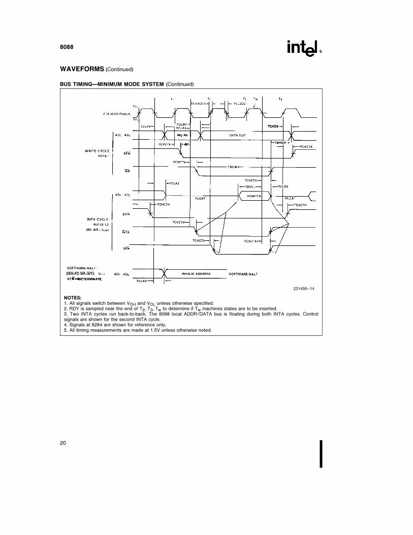
going) edge of this signal is used to latch the ad-dress information, which is valid on the address/data bus (AD0–AD7) at this time, into the8282/8283 latch. Address lines A8 through A15 donot need to be latched because they remain validthroughout the bus cycle. From T1 to T4 the IO/Msignal indicates a memory or I/O operation. At T2the address is removed from the address/data busand the bus goes to a high impedance state. Theread control signal is also asserted at T2. The read(RD) signal causes the addressed device to enableits data bus drivers to the local bus. Some time later,valid data will be available on the bus and the ad-dressed device will drive the READY line HIGH.When the processor returns the read signal to aHIGH level, the addressed device will again 3-stateits bus drivers. If a transceiver is required to bufferthe 8088 local bus, signals DT/R and DEN are pro-vided by the 8088.
A write cycle also begins with the assertion of ALEand the emission of the address. The IO/M signal isagain asserted to indicate a memory or I/O writeoperation. In T2, immediately following the addressemission, the processor emits the data to be writteninto the addressed location. This data remains validuntil at least the middle of T4. During T2, T3, andTw, the processor asserts the write control signal.The write (WR) signal becomes active at the begin-ning of T2, as opposed to the read, which is delayedsomewhat into T2 to provide time for the bus tofloat.
13
8088
The basic difference between the interrupt acknowl-edge cycle and a read cycle is that the interrupt ac-knowledge (INTA) signal is asserted in place of theread (RD) signal and the address bus is floated.(See Figure 9) In the second of two successive INTAcycles, a byte of information is read from the databus, as supplied by the interrupt system logic (i.e.8259A priority interrupt controller). This byte identi-fies the source (type) of the interrupt. It is multipliedby four and used as a pointer into the interrupt vec-tor lookup table, as described earlier.
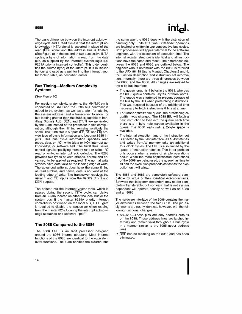
Bus TimingÐMedium ComplexitySystems
(See Figure 10)
For medium complexity systems, the MN/MX pin isconnected to GND and the 8288 bus controller isadded to the system, as well as a latch for latchingthe system address, and a transceiver to allow forbus loading greater than the 8088 is capable of han-dling. Signals ALE, DEN, and DT/R are generatedby the 8288 instead of the processor in this configu-ration, although their timing remains relatively thesame. The 8088 status outputs (S2, S1, and S0) pro-vide type of cycle information and become 8288 in-puts. This bus cycle information specifies read(code, data, or I/O), write (data or I/O), interrupt ac-knowledge, or software halt. The 8288 thus issuescontrol signals specifying memory read or write, I/Oread or write, or interrupt acknowledge. The 8288provides two types of write strobes, normal and ad-vanced, to be applied as required. The normal writestrobes have data valid at the leading edge of write.The advanced write strobes have the same timingas read strobes, and hence, data is not valid at theleading edge of write. The transceiver receives theusual T and OE inputs from the 8288’s DT/R andDEN outputs.
The pointer into the interrupt vector table, which ispassed during the second INTA cycle, can derivefrom an 8259A located on either the local bus or thesystem bus. If the master 8289A priority interruptcontroller is positioned on the local bus, a TTL gateis required to disable the transceiver when readingfrom the master 8259A during the interrupt acknowl-edge sequence and software ‘‘poll’’.
The 8088 Compared to the 8086
The 8088 CPU is an 8-bit processor designedaround the 8086 internal structure. Most internalfunctions of the 8088 are identical to the equivalent8086 functions. The 8088 handles the external bus
the same way the 8086 does with the distinction ofhandling only 8 bits at a time. Sixteen-bit operandsare fetched or written in two consecutive bus cycles.Both processors will appear identical to the softwareengineer, with the exception of execution time. Theinternal register structure is identical and all instruc-tions have the same end result. The differences be-tween the 8088 and 8086 are outlined below. Theengineer who is unfamiliar with the 8086 is referredto the iAPX 86, 88 User’s Manual, Chapters 2 and 4,for function description and instruction set informa-tion. Internally, there are three differences betweenthe 8088 and the 8086. All changes are related tothe 8-bit bus interface.
# The queue length is 4 bytes in the 8088, whereasthe 8086 queue contains 6 bytes, or three words.The queue was shortened to prevent overuse ofthe bus by the BIU when prefetching instructions.This was required because of the additional timenecessary to fetch instructions 8 bits at a time.
# To further optimize the queue, the prefetching al-gorithm was changed. The 8088 BIU will fetch anew instruction to load into the queue each timethere is a 1 byte hole (space available) in thequeue. The 8086 waits until a 2-byte space isavailable.
# The internal execution time of the instruction setis affected by the 8-bit interface. All 16-bit fetchesand writes from/to memory take an additionalfour clock cycles. The CPU is also limited by thespeed of instruction fetches. This latter problemonly occurs when a series of simple operationsoccur. When the more sophisticated instructionsof the 8088 are being used, the queue has time tofill and the execution proceeds as fast as the exe-cution unit will allow.
The 8088 and 8086 are completely software com-patible by virtue of their identical execution units.Software that is system dependent may not be com-pletely transferable, but software that is not systemdependent will operate equally as well on an 8088and an 8086.
The hardware interface of the 8088 contains the ma-jor differences between the two CPUs. The pin as-signments are nearly identical, however, with the fol-lowing functional changes:
# A8–A15ÐThese pins are only address outputson the 8088. These address lines are latched in-ternally and remain valid throughout a bus cyclein a manner similar to the 8085 upper addresslines.
# BHE has no meaning on the 8088 and has beeneliminated.
14
8088
# SSO provides the SO status information in theminimum mode. This output occurs on pin 34 inminimum mode only. DT/R, IO/M, and SSO pro-vide the complete bus status in minimum mode.
# IO/M has been inverted to be compatible with theMCS-85 bus structure.
# ALE is delayed by one clock cycle in the mini-mum mode when entering HALT, to allow thestatus to be latched with ALE.
231456–10
Figure 10. Medium Complexity System Timing
15
8088
ABSOLUTE MAXIMUM RATINGS*
Ambient Temperature Under Bias ÀÀÀÀ0§C to a70§CCase Temperature (Plastic) ÀÀÀÀÀÀÀÀÀ0§C to a95§CCase Temperature (CERDIP) ÀÀÀÀÀÀÀÀ0§C to a75§CStorage Temperature ÀÀÀÀÀÀÀÀÀÀb65§C to a150§CVoltage on Any Pin with
Respect to Ground ÀÀÀÀÀÀÀÀÀÀÀÀÀÀÀb1.0 to a7V
Power DissipationÀÀÀÀÀÀÀÀÀÀÀÀÀÀÀÀÀÀÀÀÀÀÀ2.5 Watt
NOTICE: This is a production data sheet. The specifi-cations are subject to change without notice.
*WARNING: Stressing the device beyond the ‘‘AbsoluteMaximum Ratings’’ may cause permanent damage.These are stress ratings only. Operation beyond the‘‘Operating Conditions’’ is not recommended and ex-tended exposure beyond the ‘‘Operating Conditions’’may affect device reliability.
D.C. CHARACTERISTICS(TA e 0§C to 70§C, TCASE (Plastic) e 0§C to 95§C, TCASE (CERDIP) e 0§C to 75§C,TA e 0§C to 55§C and TCASE e 0§C to 75§C for P8088-2 onlyTA is guaranteed as long as TCASE is not exceeded)
(VCC e 5V g10% for 8088, VCC e 5V g5% for 8088-2 and Extended Temperature EXPRESS)
Symbol Parameter Min Max Units Test Conditions
VIL Input Low Voltage b0.5 a0.8 V (Note 1)
VIH Input High Voltage 2.0 VCC a 0.5 V (Notes 1, 2)
VOL Output Low Voltage 0.45 V IOL e 2.0 mA
VOH Output High Voltage 2.4 V IOH e b400 mA
ICC 8088 340 mA TA e 25§CPower Supply Current: 8088-2 350
P8088 250
ILI Input Leakage Current g10 mA 0V s VIN s VCC (Note 3)
ILO Output and I/O Leakage Current g10 mA 0.45V s VOUT s VCC
VCL Clock Input Low Voltage b0.5 a0.6 V
VCH Clock Input High Voltage 3.9 VCC a 1.0 V
CIN Capacitance If Input Buffer 15 pF fc e 1 MHz
(All Input Except
AD0–AD7, RQ/GT)
CIO Capacitance of I/O Buffer 15 pF fc e 1 MHz
AD0–AD7, RQ/GT)
NOTES:1. VIL tested with MN/MX Pin e 0V
VIH tested with MN/MX Pin e 5V
MN/MX Pin is a strap Pin2. Not applicable to RQ/GT0 and RQ/GT1 Pins (Pins 30 and 31)3. HOLD and HLDA ILI Min e 30 mA, Max e 500 mA
16
8088
A.C. CHARACTERISTICS
(TA e 0§C to 70§C, TCASE (Plastic) e 0§C to 95§C, TCASE (CERDIP) e 0§C to 75§C,TA e 0§C to 55§C and TCASE e 0§C to 80§C for P8088-2 onlyTA is guaranteed as long as TCASE is not exceeded)
(VCC e 5V g10% for 8088, VCC e 5V g5% for 8088-2 and Extended Temperature EXPRESS)
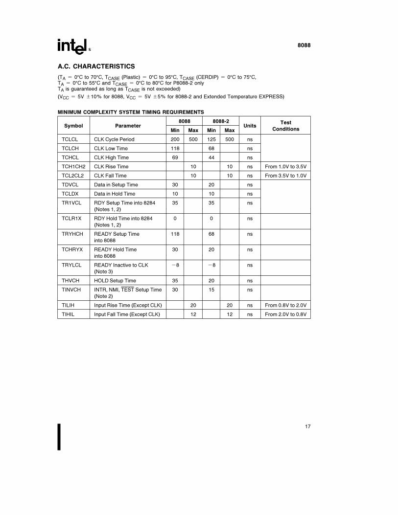
MINIMUM COMPLEXITY SYSTEM TIMING REQUIREMENTS
Symbol Parameter8088 8088-2
UnitsTest
Min Max Min Max Conditions
TCLCL CLK Cycle Period 200 500 125 500 ns
TCLCH CLK Low Time 118 68 ns
TCHCL CLK High Time 69 44 ns
TCH1CH2 CLK Rise Time 10 10 ns From 1.0V to 3.5V
TCL2CL2 CLK Fall Time 10 10 ns From 3.5V to 1.0V
TDVCL Data in Setup Time 30 20 ns
TCLDX Data in Hold Time 10 10 ns
TR1VCL RDY Setup Time into 8284 35 35 ns
(Notes 1, 2)
TCLR1X RDY Hold Time into 8284 0 0 ns
(Notes 1, 2)
TRYHCH READY Setup Time 118 68 ns
into 8088
TCHRYX READY Hold Time 30 20 ns
into 8088
TRYLCL READY Inactive to CLK b8 b8 ns
(Note 3)
THVCH HOLD Setup Time 35 20 ns
TINVCH INTR, NMI, TEST Setup Time 30 15 ns
(Note 2)
TILIH Input Rise Time (Except CLK) 20 20 ns From 0.8V to 2.0V
TIHIL Input Fall Time (Except CLK) 12 12 ns From 2.0V to 0.8V
17
8088
A.C. CHARACTERISTICS (Continued)
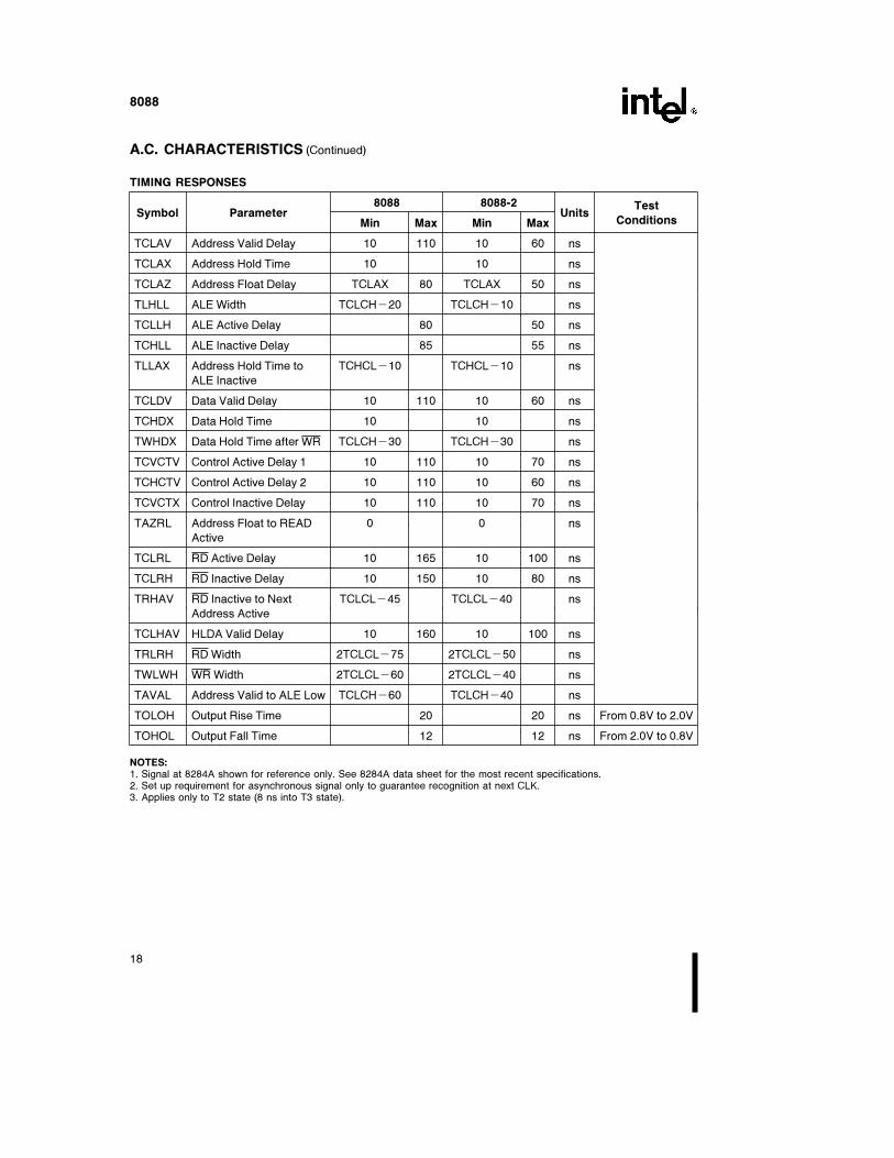
TIMING RESPONSES
Symbol Parameter8088 8088-2
UnitsTest
Min Max Min Max Conditions
TCLAV Address Valid Delay 10 110 10 60 ns
TCLAX Address Hold Time 10 10 ns
TCLAZ Address Float Delay TCLAX 80 TCLAX 50 ns
TLHLL ALE Width TCLCHb20 TCLCHb10 ns
TCLLH ALE Active Delay 80 50 ns
TCHLL ALE Inactive Delay 85 55 ns
TLLAX Address Hold Time to TCHCLb10 TCHCLb10 ns
ALE Inactive
TCLDV Data Valid Delay 10 110 10 60 ns
TCHDX Data Hold Time 10 10 ns
TWHDX Data Hold Time after WR TCLCHb30 TCLCHb30 ns
TCVCTV Control Active Delay 1 10 110 10 70 ns
TCHCTV Control Active Delay 2 10 110 10 60 ns
TCVCTX Control Inactive Delay 10 110 10 70 ns
TAZRL Address Float to READ 0 0 ns
Active
TCLRL RD Active Delay 10 165 10 100 ns
TCLRH RD Inactive Delay 10 150 10 80 ns
TRHAV RD Inactive to Next TCLCLb45 TCLCLb40 ns
Address Active
TCLHAV HLDA Valid Delay 10 160 10 100 ns
TRLRH RD Width 2TCLCLb75 2TCLCLb50 ns
TWLWH WR Width 2TCLCLb60 2TCLCLb40 ns
TAVAL Address Valid to ALE Low TCLCHb60 TCLCHb40 ns
TOLOH Output Rise Time 20 20 ns From 0.8V to 2.0V
TOHOL Output Fall Time 12 12 ns From 2.0V to 0.8V
NOTES:1. Signal at 8284A shown for reference only. See 8284A data sheet for the most recent specifications.2. Set up requirement for asynchronous signal only to guarantee recognition at next CLK.3. Applies only to T2 state (8 ns into T3 state).
18
8088
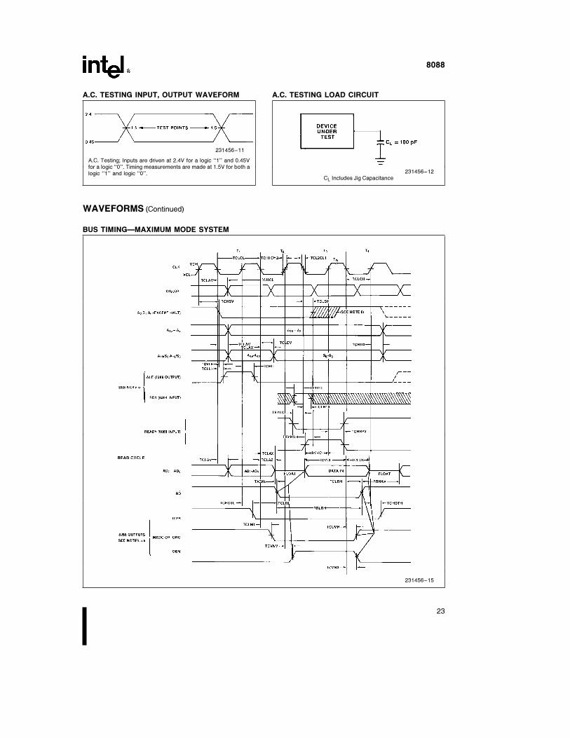
A.C. TESTING INPUT, OUTPUT WAVEFORM
231456–11
A.C. Testing; Inputs are driven at 2.4V for a logic ‘‘1’’ and 0.45Vfor a logic ‘‘0’’. Timing measurements are made at 1.5V for both alogic ‘‘1’’ and logic ‘‘0’’.
A.C. TESTING LOAD CIRCUIT
231456–12CL Includes Jig Capacitance
WAVEFORMS
BUS TIMINGÐMINIMUM MODE SYSTEM
231456–13
19
8088
WAVEFORMS (Continued)
BUS TIMINGÐMINIMUM MODE SYSTEM (Continued)
231456–14
NOTES:1. All signals switch between VOH and VOL unless otherwise specified.2. RDY is sampled near the end of T2, T3, Tw to determine if Tw machines states are to be inserted.3. Two INTA cycles run back-to-back. The 8088 local ADDR/DATA bus is floating during both INTA cycles. Controlsignals are shown for the second INTA cycle.4. Signals at 8284 are shown for reference only.5. All timing measurements are made at 1.5V unless otherwise noted.
20
8088
A.C. CHARACTERISTICS
MAX MODE SYSTEM (USING 8288 BUS CONTROLLER)
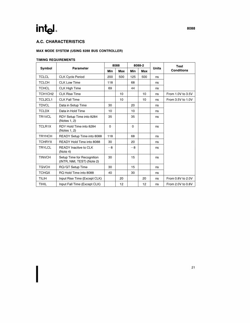
TIMING REQUIREMENTS
Symbol Parameter8088 8088-2
UnitsTest
Min Max Min Max Conditions
TCLCL CLK Cycle Period 200 500 125 500 ns
TCLCH CLK Low Time 118 68 ns
TCHCL CLK High Time 69 44 ns
TCH1CH2 CLK Rise Time 10 10 ns From 1.0V to 3.5V
TCL2CL1 CLK Fall Time 10 10 ns From 3.5V to 1.0V
TDVCL Data in Setup Time 30 20 ns
TCLDX Data in Hold Time 10 10 ns
TR1VCL RDY Setup Time into 8284 35 35 ns
(Notes 1, 2)
TCLR1X RDY Hold Time into 8284 0 0 ns
(Notes 1, 2)
TRYHCH READY Setup Time into 8088 118 68 ns
TCHRYX READY Hold Time into 8088 30 20 ns
TRYLCL READY Inactive to CLK b8 b8 ns
(Note 4)
TINVCH Setup Time for Recognition 30 15 ns
(INTR, NMI, TEST) (Note 2)
TGVCH RQ/GT Setup Time 30 15 ns
TCHGX RQ Hold Time into 8088 40 30 ns
TILIH Input Rise Time (Except CLK) 20 20 ns From 0.8V to 2.0V
TIHIL Input Fall Time (Except CLK) 12 12 ns From 2.0V to 0.8V
21
8088
A.C. CHARACTERISTICS (Continued)
TIMING RESPONSES
Symbol Parameter8088 8088-2
UnitsTest
Min Max Min Max Conditions
TCLML Command Active Delay 10 35 10 35 ns(Note 1)
TCLMH Command Inactive Delay 10 35 10 35 ns(Note 1)
TRYHSH READY Active to 110 65 nsStatus Passive (Note 3)
TCHSV Status Active Delay 10 110 10 60 ns
TCLSH Status Inactive Delay 10 130 10 70 ns
TCLAV Address Valid Delay 10 110 10 60 ns
TCLAX Address Hold Time 10 10 ns
TCLAZ Address Float Delay TCLAX 80 TCLAX 50 ns
TSVLH Status Valid to ALE High 15 15 ns(Note 1)
TSVMCH Status Valid to MCE High 15 15 ns(Note 1)
TCLLH CLK Low to ALE Valid 15 15 ns(Note 1)
TCLMCH CLK Low to MCE (Note 1) 15 15 ns
TCHLL ALE Inactive Delay (Note 1) 15 15 ns
TCLMCL MCE Inactive Delay (Note 1) 15 15 ns
TCLDV Data Valid Delay 10 110 10 60 ns
TCHDX Data Hold Time 10 10 nsCL e 20–100 pF for
TCVNV Control Active Delay 5 45 5 45 nsAll 8088 Outputs
(Note 1)in Addition to
TCVNX Control Inactive Delay 10 45 10 45 ns Internal Loads(Note 1)
TAZRL Address Float to 0 0 nsRead Active
TCLRL RD Active Delay 10 165 10 100 ns
TCLRH RD Inactive Delay 10 150 10 80 ns
TRHAV RD Inactive to Next TCLCLb45 TCLCLb40 nsAddress Active
TCHDTL Direction Control 50 50 nsActive Delay (Note 1)
TCHDTH Direction Control 30 30 nsInactive Delay (Note 1)
TCLGL GT Active Delay 85 50 ns
TCLGH GT Inactive Delay 85 50 ns
TRLRH RD Width 2TCLCLb75 2TCLCLb50 ns
TOLOH Output Rise Time 20 20 ns From 0.8V to 2.0V
TOHOL Output Fall Time 12 12 ns From 2.0V to 0.8V
NOTES:1. Signal at 8284 or 8288 shown for reference only.2. Setup requirement for asynchronous signal only to guarantee recognition at next CLK.3. Applies only to T3 and wait states.4. Applies only to T2 state (8 ns into T3 state).
22
8088
A.C. TESTING INPUT, OUTPUT WAVEFORM
231456–11
A.C. Testing; Inputs are driven at 2.4V for a logic ‘‘1’’ and 0.45Vfor a logic ‘‘0’’. Timing measurements are made at 1.5V for both alogic ‘‘1’’ and logic ‘‘0’’.
A.C. TESTING LOAD CIRCUIT
231456–12CL Includes Jig Capacitance
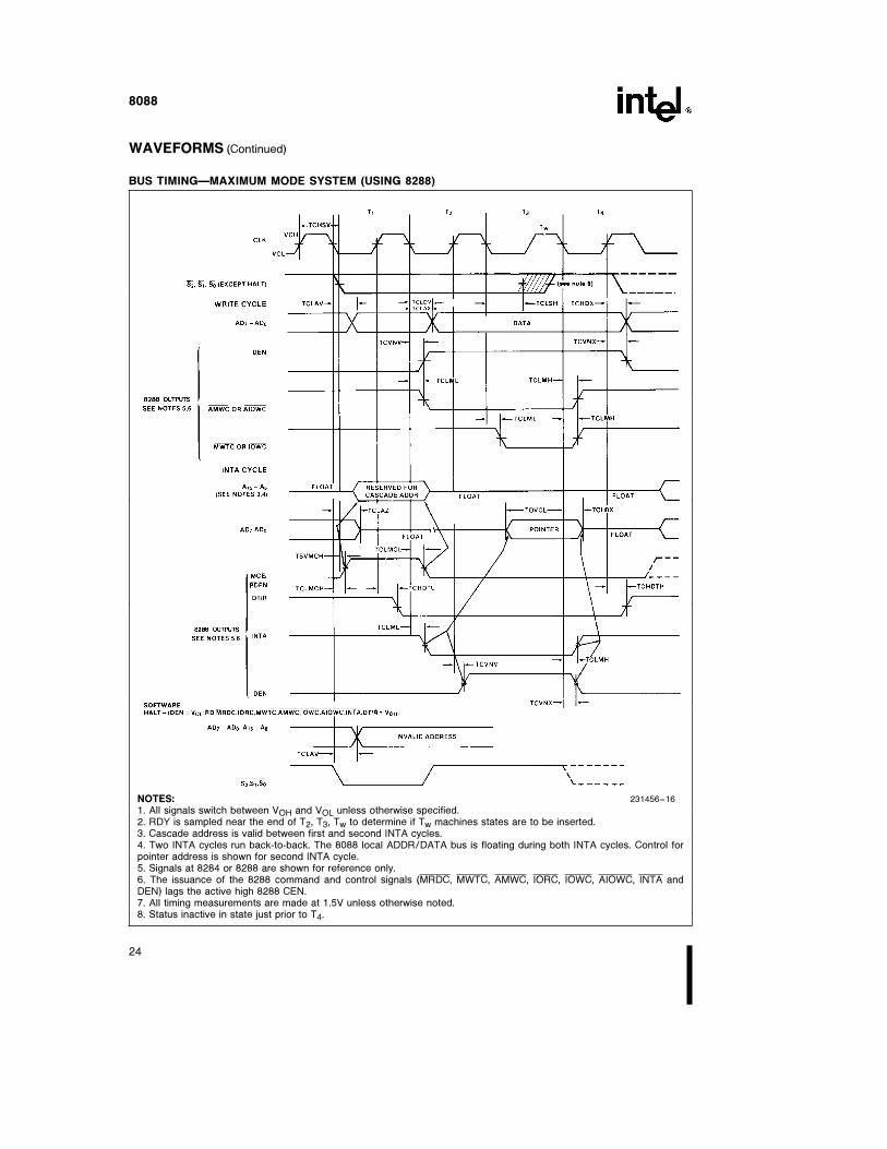
WAVEFORMS (Continued)
BUS TIMINGÐMAXIMUM MODE SYSTEM
231456–15
23
8088
WAVEFORMS (Continued)
BUS TIMINGÐMAXIMUM MODE SYSTEM (USING 8288)
NOTES: 231456–16
1. All signals switch between VOH and VOL unless otherwise specified.2. RDY is sampled near the end of T2, T3, Tw to determine if Tw machines states are to be inserted.3. Cascade address is valid between first and second INTA cycles.4. Two INTA cycles run back-to-back. The 8088 local ADDR/DATA bus is floating during both INTA cycles. Control forpointer address is shown for second INTA cycle.5. Signals at 8284 or 8288 are shown for reference only.6. The issuance of the 8288 command and control signals (MRDC, MWTC, AMWC, IORC, IOWC, AIOWC, INTA andDEN) lags the active high 8288 CEN.7. All timing measurements are made at 1.5V unless otherwise noted.8. Status inactive in state just prior to T4.
24
8088
WAVEFORMS (Continued)
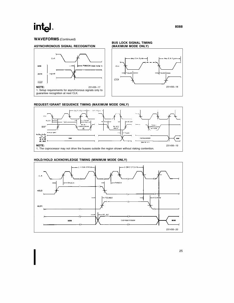
ASYNCHRONOUS SIGNAL RECOGNITION
NOTE: 231456–17
1. Setup requirements for asynchronous signals only toguarantee recognition at next CLK.
BUS LOCK SIGNAL TIMING(MAXIMUM MODE ONLY)
231456–18
REQUEST/GRANT SEQUENCE TIMING (MAXIMUM MODE ONLY)
NOTE: 231456–19
1. The coprocessor may not drive the busses outside the region shown without risking contention.
HOLD/HOLD ACKNOWLEDGE TIMING (MINIMUM MODE ONLY)
231456–20
25
8088
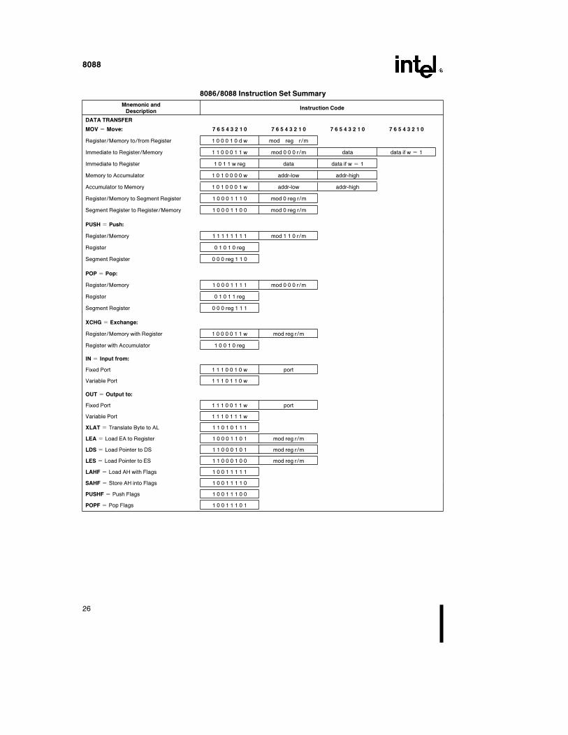
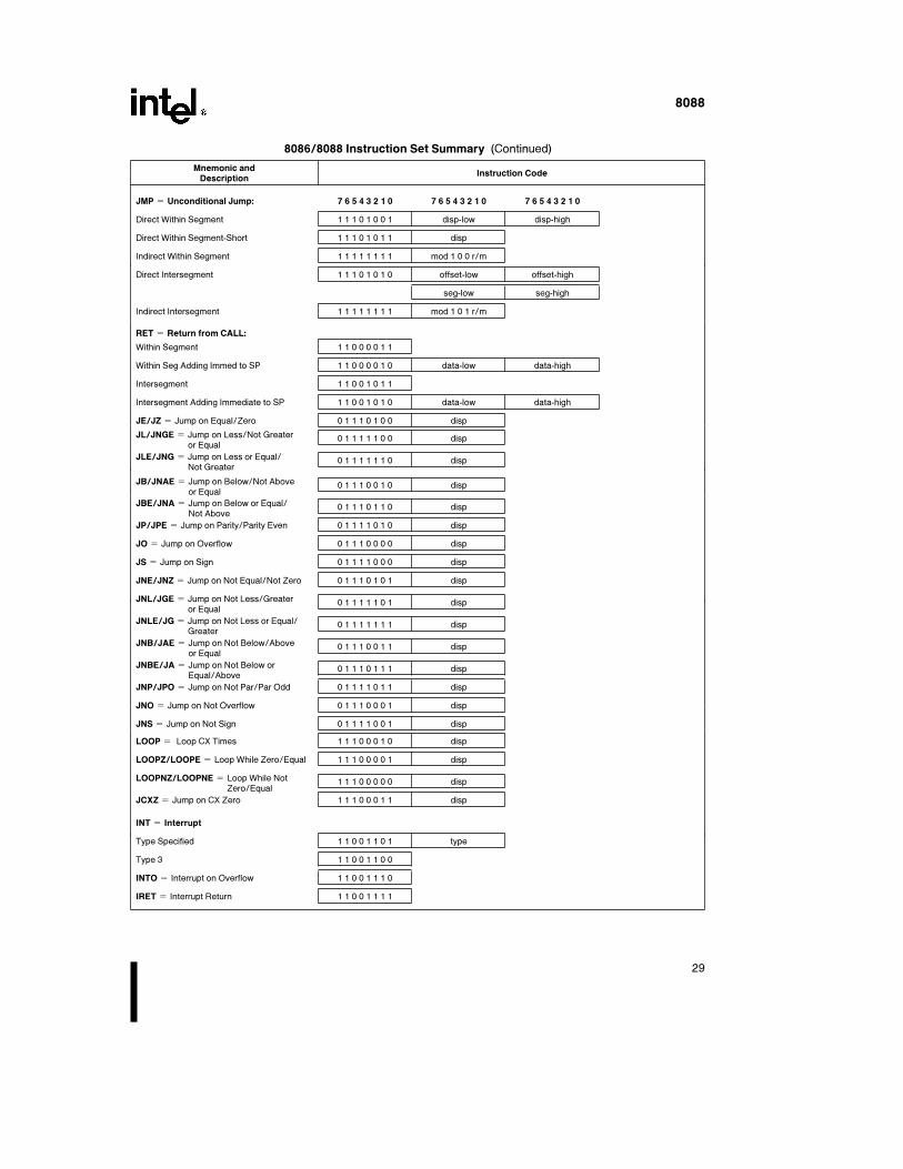
8086/8088 Instruction Set Summary
Mnemonic andInstruction Code
Description
DATA TRANSFER
MOV e Move: 7 6 5 4 3 2 1 0 7 6 5 4 3 2 1 0 7 6 5 4 3 2 1 0 7 6 5 4 3 2 1 0
Register/Memory to/from Register 1 0 0 0 1 0 d w mod reg r/m
Immediate to Register/Memory 1 1 0 0 0 1 1 w mod 0 0 0 r/m data data if w e 1
Immediate to Register 1 0 1 1 w reg data data if w e 1
Memory to Accumulator 1 0 1 0 0 0 0 w addr-low addr-high
Accumulator to Memory 1 0 1 0 0 0 1 w addr-low addr-high
Register/Memory to Segment Register 1 0 0 0 1 1 1 0 mod 0 reg r/m
Segment Register to Register/Memory 1 0 0 0 1 1 0 0 mod 0 reg r/m
PUSH e Push:
Register/Memory 1 1 1 1 1 1 1 1 mod 1 1 0 r/m
Register 0 1 0 1 0 reg
Segment Register 0 0 0 reg 1 1 0
POP e Pop:
Register/Memory 1 0 0 0 1 1 1 1 mod 0 0 0 r/m
Register 0 1 0 1 1 reg
Segment Register 0 0 0 reg 1 1 1
XCHG e Exchange:
Register/Memory with Register 1 0 0 0 0 1 1 w mod reg r/m
Register with Accumulator 1 0 0 1 0 reg
IN e Input from:
Fixed Port 1 1 1 0 0 1 0 w port
Variable Port 1 1 1 0 1 1 0 w
OUT e Output to:
Fixed Port 1 1 1 0 0 1 1 w port
Variable Port 1 1 1 0 1 1 1 w
XLAT e Translate Byte to AL 1 1 0 1 0 1 1 1
LEA e Load EA to Register 1 0 0 0 1 1 0 1 mod reg r/m
LDS e Load Pointer to DS 1 1 0 0 0 1 0 1 mod reg r/m
LES e Load Pointer to ES 1 1 0 0 0 1 0 0 mod reg r/m
LAHF e Load AH with Flags 1 0 0 1 1 1 1 1
SAHF e Store AH into Flags 1 0 0 1 1 1 1 0
PUSHF e Push Flags 1 0 0 1 1 1 0 0
POPF e Pop Flags 1 0 0 1 1 1 0 1
26
8088
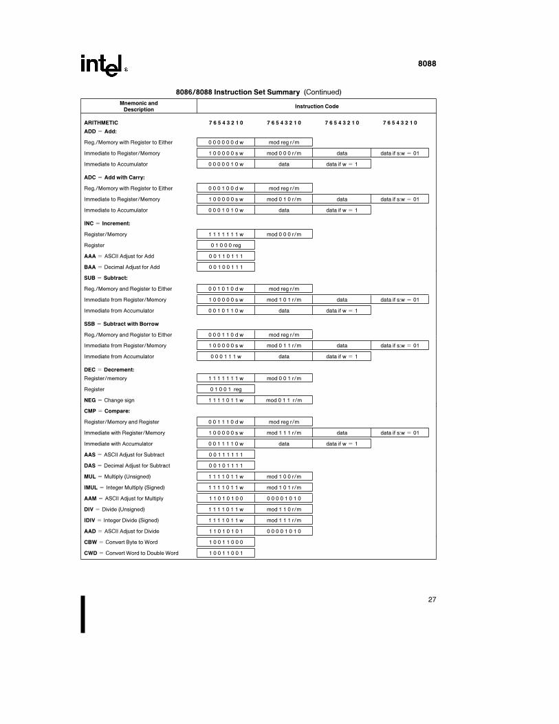
8086/8088 Instruction Set Summary (Continued)
Mnemonic andInstruction Code
Description
ARITHMETIC 7 6 5 4 3 2 1 0 7 6 5 4 3 2 1 0 7 6 5 4 3 2 1 0 7 6 5 4 3 2 1 0
ADD e Add:
Reg./Memory with Register to Either 0 0 0 0 0 0 d w mod reg r/m
Immediate to Register/Memory 1 0 0 0 0 0 s w mod 0 0 0 r/m data data if s:w e 01
Immediate to Accumulator 0 0 0 0 0 1 0 w data data if w e 1
ADC e Add with Carry:
Reg./Memory with Register to Either 0 0 0 1 0 0 d w mod reg r/m
Immediate to Register/Memory 1 0 0 0 0 0 s w mod 0 1 0 r/m data data if s:w e 01
Immediate to Accumulator 0 0 0 1 0 1 0 w data data if w e 1
INC e Increment:
Register/Memory 1 1 1 1 1 1 1 w mod 0 0 0 r/m
Register 0 1 0 0 0 reg
AAA e ASCII Adjust for Add 0 0 1 1 0 1 1 1
BAA e Decimal Adjust for Add 0 0 1 0 0 1 1 1
SUB e Subtract:
Reg./Memory and Register to Either 0 0 1 0 1 0 d w mod reg r/m
Immediate from Register/Memory 1 0 0 0 0 0 s w mod 1 0 1 r/m data data if s:w e 01
Immediate from Accumulator 0 0 1 0 1 1 0 w data data if w e 1
SSB e Subtract with Borrow
Reg./Memory and Register to Either 0 0 0 1 1 0 d w mod reg r/m
Immediate from Register/Memory 1 0 0 0 0 0 s w mod 0 1 1 r/m data data if s:w e 01
Immediate from Accumulator 0 0 0 1 1 1 w data data if w e 1
DEC e Decrement:
Register/memory 1 1 1 1 1 1 1 w mod 0 0 1 r/m
Register 0 1 0 0 1 reg
NEG e Change sign 1 1 1 1 0 1 1 w mod 0 1 1 r/m
CMP e Compare:
Register/Memory and Register 0 0 1 1 1 0 d w mod reg r/m
Immediate with Register/Memory 1 0 0 0 0 0 s w mod 1 1 1 r/m data data if s:w e 01
Immediate with Accumulator 0 0 1 1 1 1 0 w data data if w e 1
AAS e ASCII Adjust for Subtract 0 0 1 1 1 1 1 1
DAS e Decimal Adjust for Subtract 0 0 1 0 1 1 1 1
MUL e Multiply (Unsigned) 1 1 1 1 0 1 1 w mod 1 0 0 r/m
IMUL e Integer Multiply (Signed) 1 1 1 1 0 1 1 w mod 1 0 1 r/m
AAM e ASCII Adjust for Multiply 1 1 0 1 0 1 0 0 0 0 0 0 1 0 1 0
DIV e Divide (Unsigned) 1 1 1 1 0 1 1 w mod 1 1 0 r/m
IDIV e Integer Divide (Signed) 1 1 1 1 0 1 1 w mod 1 1 1 r/m
AAD e ASCII Adjust for Divide 1 1 0 1 0 1 0 1 0 0 0 0 1 0 1 0
CBW e Convert Byte to Word 1 0 0 1 1 0 0 0
CWD e Convert Word to Double Word 1 0 0 1 1 0 0 1
27
8088
8086/8088 Instruction Set Summary (Continued)
Mnemonic andInstruction Code
Description
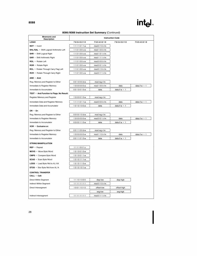
LOGIC 7 6 5 4 3 2 1 0 7 6 5 4 3 2 1 0 7 6 5 4 3 2 1 0 7 6 5 4 3 2 1 0
NOT e Invert 1 1 1 1 0 1 1 w mod 0 1 0 r/m
SHL/SAL e Shift Logical/Arithmetic Left 1 1 0 1 0 0 v w mod 1 0 0 r/m
SHR e Shift Logical Right 1 1 0 1 0 0 v w mod 1 0 1 r/m
SAR e Shift Arithmetic Right 1 1 0 1 0 0 v w mod 1 1 1 r/m
ROL e Rotate Left 1 1 0 1 0 0 v w mod 0 0 0 r/m
ROR e Rotate Right 1 1 0 1 0 0 v w mod 0 0 1 r/m
RCL e Rotate Through Carry Flag Left 1 1 0 1 0 0 v w mod 0 1 0 r/m
RCR e Rotate Through Carry Right 1 1 0 1 0 0 v w mod 0 1 1 r/m
AND e And:
Reg./Memory and Register to Either 0 0 1 0 0 0 d w mod reg r/m
Immediate to Register/Memory 1 0 0 0 0 0 0 w mod 1 0 0 r/m data data if w e 1
Immediate to Accumulator 0 0 1 0 0 1 0 w data data if w e 1
TEST e And Function to Flags. No Result:
Register/Memory and Register 1 0 0 0 0 1 0 w mod reg r/m
Immediate Data and Register/Memory 1 1 1 1 0 1 1 w mod 0 0 0 r/m data data if w e 1
Immediate Data and Accumulator 1 0 1 0 1 0 0 w data data if w e 1
OR e Or:
Reg./Memory and Register to Either 0 0 0 0 1 0 d w mod reg r/m
Immediate to Register/Memory 1 0 0 0 0 0 0 w mod 0 0 1 r/m data data if w e 1
Immediate to Accumulator 0 0 0 0 1 1 0 w data data if w e 1
XOR e Exclusive or:
Reg./Memory and Register to Either 0 0 1 1 0 0 d w mod reg r/m
Immediate to Register/Memory 1 0 0 0 0 0 0 w mod 1 1 0 r/m data data if w e 1
Immediate to Accumulator 0 0 1 1 0 1 0 w data data if w e 1
STRING MANIPULATION
REP e Repeat 1 1 1 1 0 0 1 z
MOVS e Move Byte/Word 1 0 1 0 0 1 0 w
CMPS e Compare Byte/Word 1 0 1 0 0 1 1 w
SCAS e Scan Byte/Word 1 0 1 0 1 1 1 w
LODS e Load Byte/Wd to AL/AX 1 0 1 0 1 1 0 w
STOS e Stor Byte/Wd from AL/A 1 0 1 0 1 0 1 w
CONTROL TRANSFER
CALL e Call:
Direct Within Segment 1 1 1 0 1 0 0 0 disp-low disp-high
Indirect Within Segment 1 1 1 1 1 1 1 1 mod 0 1 0 r/m
Direct Intersegment 1 0 0 1 1 0 1 0 offset-low offset-high
seg-low seg-high
Indirect Intersegment 1 1 1 1 1 1 1 1 mod 0 1 1 r/m
28
8088
8086/8088 Instruction Set Summary (Continued)
Mnemonic andInstruction Code
Description
JMP e Unconditional Jump: 7 6 5 4 3 2 1 0 7 6 5 4 3 2 1 0 7 6 5 4 3 2 1 0
Direct Within Segment 1 1 1 0 1 0 0 1 disp-low disp-high
Direct Within Segment-Short 1 1 1 0 1 0 1 1 disp
Indirect Within Segment 1 1 1 1 1 1 1 1 mod 1 0 0 r/m
Direct Intersegment 1 1 1 0 1 0 1 0 offset-low offset-high
seg-low seg-high
Indirect Intersegment 1 1 1 1 1 1 1 1 mod 1 0 1 r/m
RET e Return from CALL:
Within Segment 1 1 0 0 0 0 1 1
Within Seg Adding Immed to SP 1 1 0 0 0 0 1 0 data-low data-high
Intersegment 1 1 0 0 1 0 1 1
Intersegment Adding Immediate to SP 1 1 0 0 1 0 1 0 data-low data-high
JE/JZ e Jump on Equal/Zero 0 1 1 1 0 1 0 0 disp
JL/JNGE e Jump on Less/Not Greater 0 1 1 1 1 1 0 0 dispor Equal
JLE/JNG e Jump on Less or Equal/ 0 1 1 1 1 1 1 0 dispNot Greater
JB/JNAE e Jump on Below/Not Above 0 1 1 1 0 0 1 0 dispor Equal
JBE/JNA e Jump on Below or Equal/ 0 1 1 1 0 1 1 0 dispNot Above
JP/JPE e Jump on Parity/Parity Even 0 1 1 1 1 0 1 0 disp
JO e Jump on Overflow 0 1 1 1 0 0 0 0 disp
JS e Jump on Sign 0 1 1 1 1 0 0 0 disp
JNE/JNZ e Jump on Not Equal/Not Zero 0 1 1 1 0 1 0 1 disp
JNL/JGE e Jump on Not Less/Greater 0 1 1 1 1 1 0 1 dispor Equal
JNLE/JG e Jump on Not Less or Equal/ 0 1 1 1 1 1 1 1 dispGreater
JNB/JAE e Jump on Not Below/Above 0 1 1 1 0 0 1 1 dispor Equal
JNBE/JA e Jump on Not Below or 0 1 1 1 0 1 1 1 dispEqual/Above
JNP/JPO e Jump on Not Par/Par Odd 0 1 1 1 1 0 1 1 disp
JNO e Jump on Not Overflow 0 1 1 1 0 0 0 1 disp
JNS e Jump on Not Sign 0 1 1 1 1 0 0 1 disp
LOOP e Loop CX Times 1 1 1 0 0 0 1 0 disp
LOOPZ/LOOPE e Loop While Zero/Equal 1 1 1 0 0 0 0 1 disp
LOOPNZ/LOOPNE e Loop While Not 1 1 1 0 0 0 0 0 dispZero/Equal
JCXZ e Jump on CX Zero 1 1 1 0 0 0 1 1 disp
INT e Interrupt
Type Specified 1 1 0 0 1 1 0 1 type
Type 3 1 1 0 0 1 1 0 0
INTO e Interrupt on Overflow 1 1 0 0 1 1 1 0
IRET e Interrupt Return 1 1 0 0 1 1 1 1
29
8088
8086/8088 Instruction Set Summary (Continued)
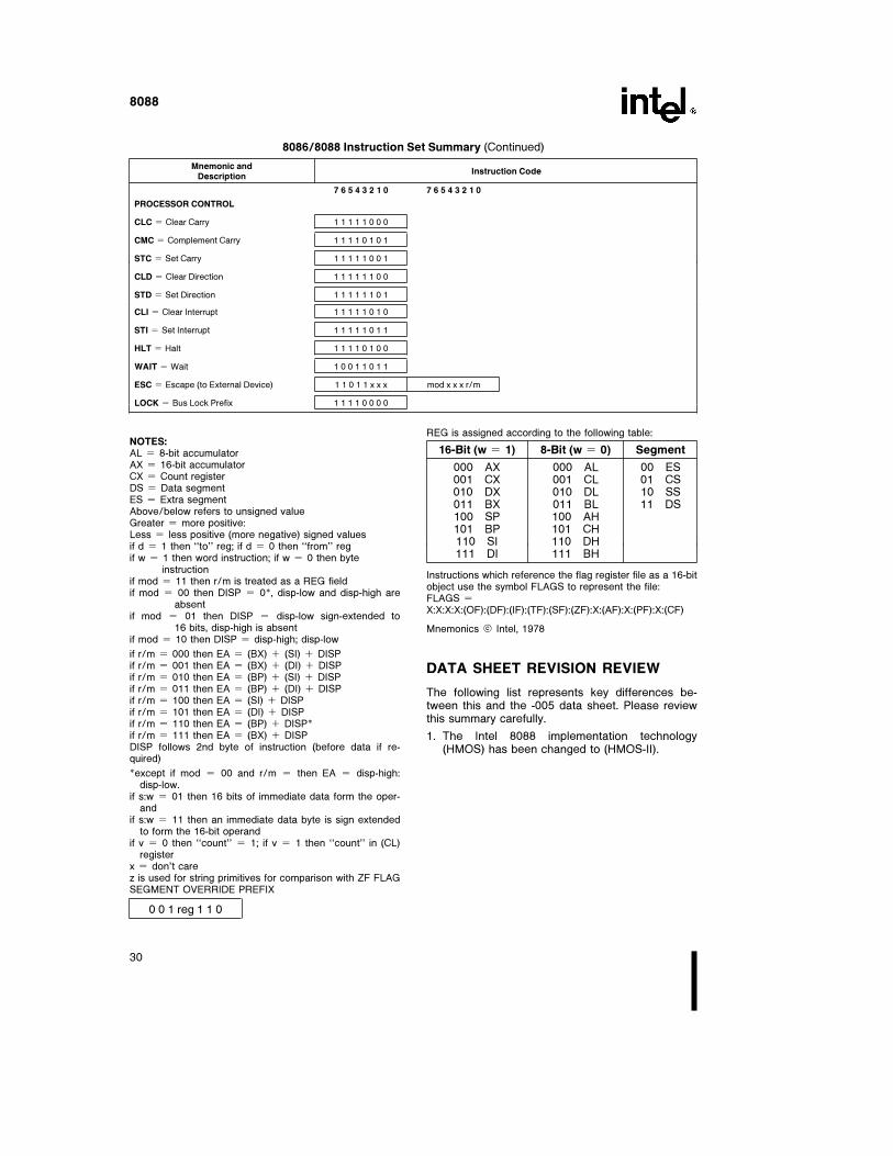
Mnemonic andInstruction Code
Description
7 6 5 4 3 2 1 0 7 6 5 4 3 2 1 0
PROCESSOR CONTROL
CLC e Clear Carry 1 1 1 1 1 0 0 0
CMC e Complement Carry 1 1 1 1 0 1 0 1
STC e Set Carry 1 1 1 1 1 0 0 1
CLD e Clear Direction 1 1 1 1 1 1 0 0
STD e Set Direction 1 1 1 1 1 1 0 1
CLI e Clear Interrupt 1 1 1 1 1 0 1 0
STI e Set Interrupt 1 1 1 1 1 0 1 1
HLT e Halt 1 1 1 1 0 1 0 0
WAIT e Wait 1 0 0 1 1 0 1 1
ESC e Escape (to External Device) 1 1 0 1 1 x x x mod x x x r/m
LOCK e Bus Lock Prefix 1 1 1 1 0 0 0 0
NOTES:AL e 8-bit accumulatorAX e 16-bit accumulatorCX e Count registerDS e Data segmentES e Extra segmentAbove/below refers to unsigned valueGreater e more positive:Less e less positive (more negative) signed valuesif d e 1 then ‘‘to’’ reg; if d e 0 then ‘‘from’’ regif w e 1 then word instruction; if w e 0 then byte
instructionif mod e 11 then r/m is treated as a REG fieldif mod e 00 then DISP e 0*, disp-low and disp-high are
absentif mod e 01 then DISP e disp-low sign-extended to
16 bits, disp-high is absentif mod e 10 then DISP e disp-high; disp-low
if r/m e 000 then EA e (BX) a (SI) a DISPif r/m e 001 then EA e (BX) a (DI) a DISPif r/m e 010 then EA e (BP) a (SI) a DISPif r/m e 011 then EA e (BP) a (DI) a DISPif r/m e 100 then EA e (SI) a DISPif r/m e 101 then EA e (DI) a DISPif r/m e 110 then EA e (BP) a DISP*if r/m e 111 then EA e (BX) a DISPDISP follows 2nd byte of instruction (before data if re-quired)
*except if mod e 00 and r/m e then EA e disp-high:disp-low.
if s:w e 01 then 16 bits of immediate data form the oper-and
if s:w e 11 then an immediate data byte is sign extendedto form the 16-bit operand
if v e 0 then ‘‘count’’ e 1; if v e 1 then ‘‘count’’ in (CL)register
x e don’t carez is used for string primitives for comparison with ZF FLAGSEGMENT OVERRIDE PREFIX
0 0 1 reg 1 1 0
REG is assigned according to the following table:
16-Bit (w e 1) 8-Bit (w e 0) Segment
000 AX 000 AL 00 ES001 CX 001 CL 01 CS010 DX 010 DL 10 SS011 BX 011 BL 11 DS100 SP 100 AH101 BP 101 CH110 SI 110 DH111 DI 111 BH
Instructions which reference the flag register file as a 16-bitobject use the symbol FLAGS to represent the file:FLAGS e
X:X:X:X:(OF):(DF):(IF):(TF):(SF):(ZF):X:(AF):X:(PF):X:(CF)
Mnemonics © Intel, 1978
DATA SHEET REVISION REVIEW
The following list represents key differences be-tween this and the -005 data sheet. Please reviewthis summary carefully.
1. The Intel 8088 implementation technology(HMOS) has been changed to (HMOS-II).
30


![Weeks 4-5 8088/8086 Microprocessor Programmingalkar/ELE414/dirz2005/w4-414-[2005].pdf · 8088/8086 Microprocessor Programming . 2 ... 80x86 Interrupts • An interrupt is an event](https://static.fdocuments.net/doc/165x107/5e70a945fb5d632d193db492/weeks-4-5-80888086-microprocessor-alkarele414dirz2005w4-414-2005pdf-80888086.jpg)