
8051 PROGRAM-HC-PM51-V5 User Manual
59
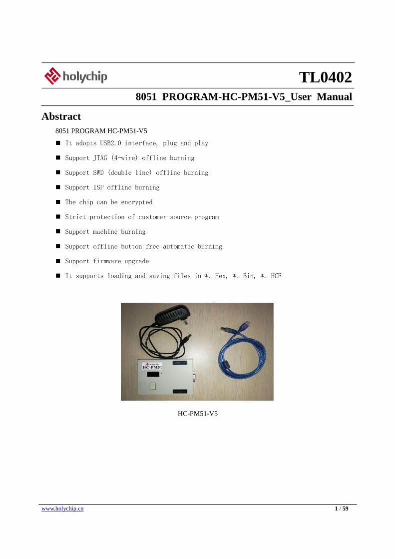
www.holychip.cn 1 / 59 TL0402 8051 PROGRAM-HC-PM51-V5_User Manual Abstract 8051 PROGRAM HC-PM51-V5 It adopts USB2.0 interface, plug and play Support JTAG (4-wire) offline burning Support SWD (double line) offline burning Support ISP offline burning The chip can be encrypted Strict protection of customer source program Support machine burning Support offline button free automatic burning Support firmware upgrade It supports loading and saving files in *. Hex, *. Bin, *. HCF HC-PM51-V5
Transcript of 8051 PROGRAM-HC-PM51-V5 User Manual
www.holychip.cn 1 / 59
TL0402
8051 PROGRAM-HC-PM51-V5_User Manual
Abstract
8051 PROGRAM HC-PM51-V5
It adopts USB2.0 interface, plug and play
Support JTAG (4-wire) offline burning
Support SWD (double line) offline burning
Support ISP offline burning
The chip can be encrypted
Strict protection of customer source program
Support machine burning
Support offline button free automatic burning
Support firmware upgrade
It supports loading and saving files in *. Hex, *. Bin, *. HCF
HC-PM51-V5

TL0402
www.holychip.cn 2 / 59
Contents
1 SOFTWARE INSTALLATION .......................................................................................................................... 4
2 HARDWARE CONNECTION............................................................................................................................ 4
3 MASS PRODUCTION ........................................................................................................................................ 5
3.1 OPEN PROGRAM FILE ............................................................................................................................................ 5
3.2 DOWNLOAD PROGRAM FILE .................................................................................................................................. 6
3.3 MANUAL PROGRAM .............................................................................................................................................. 7
3.4 READ CODE CRC ................................................................................................................................................ 8
3.5 MACHINE PROGRAM ............................................................................................................................................. 8
4 R&D MODE ......................................................................................................................................................... 9
4.1 SELECT MCU ...................................................................................................................................................... 10
4.2 LOAD CODE/EEPROM ...................................................................................................................................... 11
4.3 MCU PROTECTION .............................................................................................................................................. 12
4.4 SELECT JTAG/SWD ............................................................................................................................................ 13
4.5 PROGRAM VOLTAGE ............................................................................................................................................ 14
4.6 OFFLINE AUTO PROGRAM ................................................................................................................................... 14
4.7 PROGRAM SETTINGS ........................................................................................................................................... 14
4.8 SAVE PROGRAM FILE ........................................................................................................................................... 15
4.9 DOWNLOAD AND PROGRAM ................................................................................................................................ 15
4.10 ONLINE OPERATION .......................................................................................................................................... 16
4.11 READ MCU ....................................................................................................................................................... 16
4.12 EDIT .................................................................................................................................................................. 16
4.13 OFFLINE PROGRAM ISP FIRMWARE ................................................................................................................... 17
4.14 RESTORE FACTORY SETTINGS ............................................................................................................................ 17
4.15 CALIBRATION SETTINGS .................................................................................................................................... 17
4.16 QUERY DEVICE U_ID ........................................................................................................................................ 17
5 SOFTWARE AND FIRMWARE UPDATE ..................................................................................................... 18
5.1 SOFTWARE UPDATE ............................................................................................................................................. 18
5.2 FIRMWARE UPDATE ............................................................................................................................................. 18
6 PROGRAM SOCKET BOARD ........................................................................................................................ 19
6.1 HC89S001P-SOP8-ISP ................................................................................................................................ 20
6.2 HC89S003F4-TSSOP20-ISP&JTAG........................................................................................................... 21
6.3 HC89S003F4-QFN20-ISP&JTAG .............................................................................................................. 22
6.4 HC89S103K6-LQFP32-ISP&SWD&JTAG ................................................................................................ 23
6.5 HC89S105K8-LQFP32-ISP&JTAG ............................................................................................................ 24
6.6 HC89S105S8-LQFP44-ISP&JTAG ............................................................................................................. 25
6.7 HC89S105C8-LQFP48-ISP&JTAG ............................................................................................................ 26
6.8 HC89F0411P-SOP8-ISP .............................................................................................................................. 27
6.9 HC89F0421-SOP16-ISP&JTAG ................................................................................................................. 28

TL0402
www.holychip.cn 3 / 59
6.10 HC89F0431-SOP20/TSSOP20-ISP&JTAG ................................................................................................ 29
6.11 HC89F0431-QFN20-JTAG.......................................................................................................................... 30
6.12 HC89F0531-SOP20/TSSOP20-SWD&JTAG ............................................................................................. 31
6.13 HC89F0531-SSOP24-SWD&JTAG ............................................................................................................ 32
6.14 HC89F0531-QFN24-SWD&JTAG .............................................................................................................. 33
6.15 HC89F0541-SOP28/SSOP28-SWD&JTAG ................................................................................................ 34
6.16 HC89F0541-LQFP32/QFN32-SWD&JTAG ............................................................................................... 35
6.17 HC89F0650-LQFP44-ISP&JTAG ............................................................................................................... 36
6.18 HC89F0650-LQFP48-ISP&JTAG ............................................................................................................... 37
6.19 HC8M602-SOP16-SWD ............................................................................................................................. 38
6.20 HC89F301-SOP16-SWD ............................................................................................................................. 39
6.21 HC89F301B-SOP16-SWD .......................................................................................................................... 40
6.22 HC89F302-SOP20/DIP20-SWD ................................................................................................................. 41
6.23 HC89F302-SOP24-SWD ............................................................................................................................. 42
6.24 HC89F302B-SOP20/DIP20-SWD ............................................................................................................... 43
6.25 HC89F302B-SOP24-SWD .......................................................................................................................... 44
6.26 HC89F303-SOP28-SWD ............................................................................................................................. 45
6.27 HC89F303B-SOP28-SWD .......................................................................................................................... 46
6.28 HC89F3421-SOP16-SWD ........................................................................................................................... 47
6.29 HC89F3421-SOP16-JTAG .......................................................................................................................... 48
6.30 HC89F3531-SOP20/DIP20-SWD ............................................................................................................... 49
6.31 HC89F3531-SOP20/DIP20-JTAG ............................................................................................................... 50
6.32 HC89F3531-SOP24-SWD ........................................................................................................................... 51
6.33 HC89F3531-SOP24-JTAG .......................................................................................................................... 52
6.34 HC89F3541-SOP28-SWD ........................................................................................................................... 53
6.35 HC89F3541-SOP28-JTAG .......................................................................................................................... 54
6.36 HC89F3541-LQFP32-SWD ........................................................................................................................ 55
6.37 HC89F3541-LQFP32-JTAG ........................................................................................................................ 56
6.38 HC89F3650-LQFP44-JTAG ........................................................................................................................ 57
6.39 HC89F3650-LQFP48-JTAG ........................................................................................................................ 58
7 VERSION DESCRIPTION ............................................................................................................................... 59
TL0402
www.holychip.cn 4 / 59
1 Software Installation Please refer to 《TL0001_Driver Install Manual》and《TL0401_8051 PROGRAM_HC-PM51-V5_Install
Manual》。
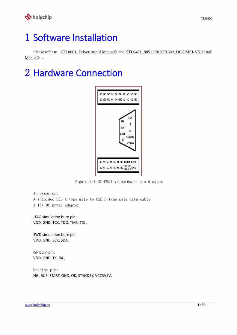
2 Hardware Connection
Figure 2-1 HC-PM51-V5 hardware pin diagram
Accessories:
A shielded USB A-type male to USB B-type male data cable
A 15V DC power adapter
JTAG simulation burn pin:
VDD, GND, TCK, TDO, TMS, TDI。
SWD simulation burn pin:
VDD, GND, SCK, SDA。
ISP burn pin:
VDD, GND, TX, RX。
Machine pin:
NG, BUS, START, GND, OK, STANDBY, VCC3V5V。
TL0402
www.holychip.cn 5 / 59
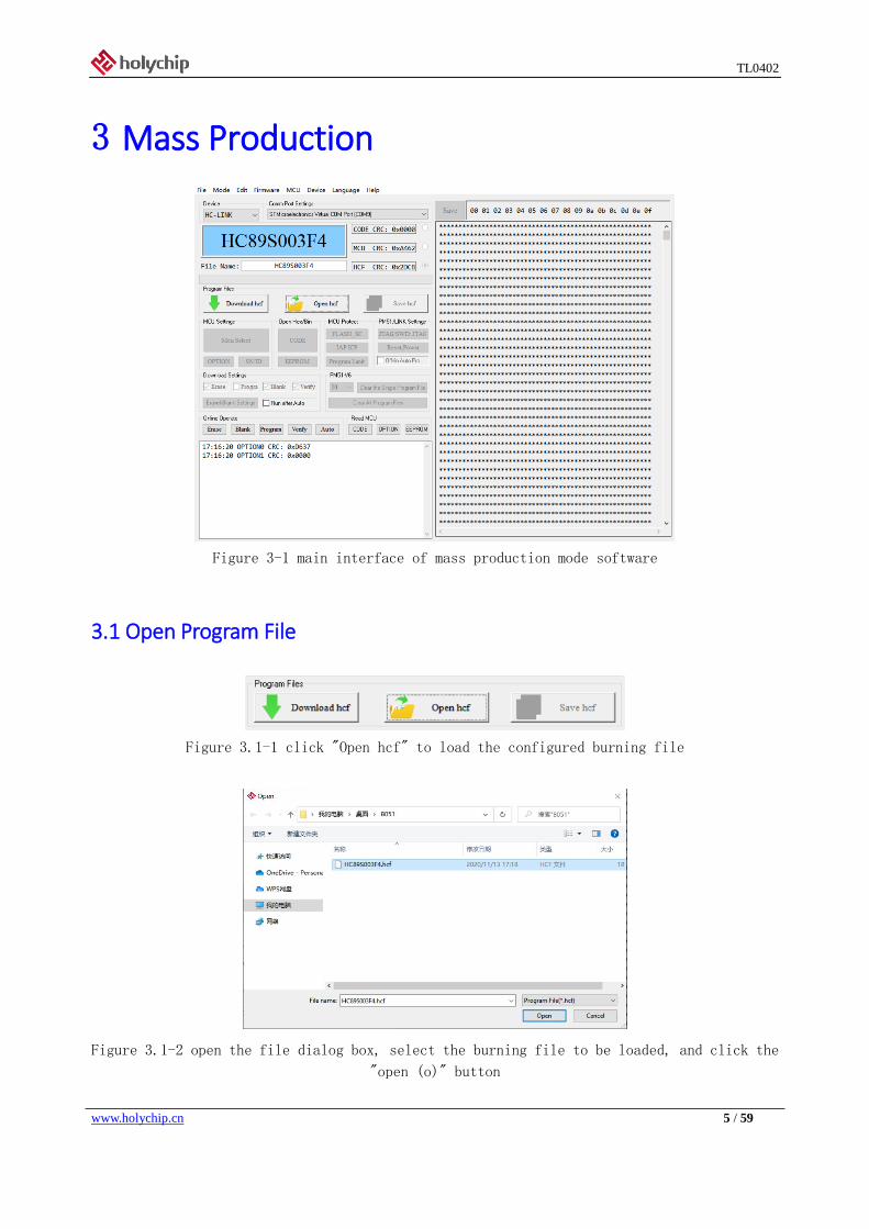
3 Mass Production
Figure 3-1 main interface of mass production mode software
3.1 Open Program File
Figure 3.1-1 click "Open hcf" to load the configured burning file
Figure 3.1-2 open the file dialog box, select the burning file to be loaded, and click the
"open (o)" button

TL0402
www.holychip.cn 6 / 59
Figure 3.1-3 confirm chip model
Figure 3.1-4 confirmation of code CRC, MCU CRC and HCF CRC
3.2 Download Program File
Figure 3.2-1 hc-pm51-v5 is connected to the computer through USB cable. Select "hc-pm51" to
confirm the device port
Figure 3.2-2 software main interface, click "download HCF" button to start downloading burning
files
Figure 3.2-3 burning file downloading, please wait patiently
Figure 3.2-4 successful download of burning file
Figure 3.2-5 hc-pm51-v5 display screen confirms chip model and CRC, and LED lights up green
TL0402
www.holychip.cn 7 / 59
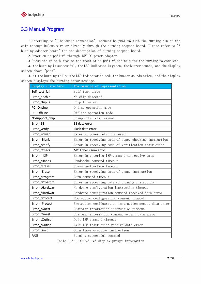
3.3 Manual Program
1. Referring to "2 hardware connection", connect hc-pm51-v5 with the burning pin of the
chip through DuPont wire or directly through the burning adapter board. Please refer to "6
burning adapter board" for the description of burning adapter board.
2. Power on hc-pm51-v5 through 15V DC power adapter.
3. Press the white button on the front of hc-pm51-v5 and wait for the burning to complete.
4. the burning is successful, the LED indicator is green, the buzzer sounds, and the display
screen shows "pass".
3. if the burning fails, the LED indicator is red, the buzzer sounds twice, and the display
screen displays the burning error message.
Display characters The meaning of representation
Self_test_fail Self test error
Error_nochip No chip detected
Error_chipID Chip ID error
PC--OnLine Online operation mode
PC--OffLine Offline operation mode
Nosupport_chip Unsupported chip signal
Error_EE EE data error
Error_verify Flash data error
Error_Power External power detection error
Error_rBlank Error in receiving data of space checking instruction
Error_rVerify Error in receiving data of verification instruction
Error_rCheck MCU check sum error
Error_inISP Error in entering ISP command to receive data
Error_tHands Handshake command timeout
Error_tErase Erase instruction timeout
Error_rErase Error in receiving data of erase instruction
Error_tProgrom Burn command timeout
Error_rProgrom Error in receiving data of burning instruction
Error_tHardwar Hardware configuration instruction timeout
Error_rHardwar Hardware configuration command received data error
Error_tProtect Protection configuration command timeout
Error_rProtect Protection configuration instruction accept data error
Error_tGuest Customer information instruction timeout
Error_rGuest Customer information command accept data error
Error_tOutisp Quit ISP command timeout
Error_rOutisp Exit ISP instruction receive data error
Error_Limit Burn times overflow instruction
PASS Burning successful command
Table 3.3-1 HC-PM51-V5 display prompt information
TL0402
www.holychip.cn 8 / 59
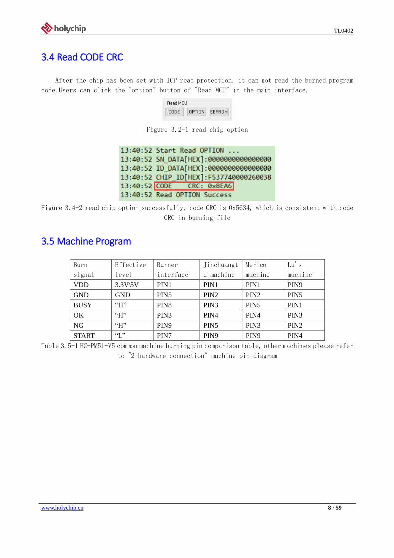
3.4 Read CODE CRC
After the chip has been set with ICP read protection, it can not read the burned program
code.Users can click the "option" button of "Read MCU" in the main interface.
Figure 3.2-1 read chip option
Figure 3.4-2 read chip option successfully, code CRC is 0x5634, which is consistent with code
CRC in burning file
3.5 Machine Program
Burn
signal
Effective
level
Burner
interface
Jinchuangt
u machine
Merico
machine
Lu's
machine
VDD 3.3V\5V PIN1 PIN1 PIN1 PIN9
GND GND PIN5 PIN2 PIN2 PIN5
BUSY “H” PIN8 PIN3 PIN5 PIN1
OK “H” PIN3 PIN4 PIN4 PIN3
NG “H” PIN9 PIN5 PIN3 PIN2
START “L” PIN7 PIN9 PIN9 PIN4
Table 3.5-1 HC-PM51-V5 common machine burning pin comparison table, other machines please refer
to "2 hardware connection" machine pin diagram
TL0402
www.holychip.cn 9 / 59
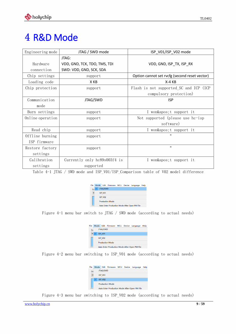
4 R&D Mode Engineering mode JTAG / SWD mode ISP_V01/ISP_V02 mode
Hardware
connection
JTAG:
VDD, GND, TCK, TDO, TMS, TDI
SWD: VDD, GND, SCK, SDA
VDD, GND, ISP_TX, ISP_RX
Chip settings support Option cannot set rvcfg (second reset vector)
Loading code X KB X-4 KB
Chip protection support Flash is not supported_SC and ICP (ICP
compulsory protection)
Communication
mode
JTAG/SWD ISP
Burn settings support I won't support it
Online operation support Not supported (please use hc-isp
software)
Read chip support I won't support it
Offline burning
ISP firmware
support "
Restore factory
settings
support "
Calibration
settings
Currently only hc89s003f4 is
supported
I won't support it
Table 4-1 JTAG / SWD mode and ISP_V01/ISP_Comparison table of V02 model difference
Figure 4-1 menu bar switch to JTAG / SWD mode (according to actual needs)
Figure 4-2 menu bar switching to ISP_V01 mode (according to actual needs)
Figure 4-3 menu bar switching to ISP_V02 mode (according to actual needs)

TL0402
www.holychip.cn 10 / 59
4.1 Select MCU
Figure 4.1-1 select MCU interface
Figure 4.1-2 chip model selection dialog box, select chip model and click "OK" button to exit
Figure 4.1-3 option settings. Please refer to the chip data manual for details
Figure 4.1-4 SN_DATA、ID_Please refer to the chip data manual for details
TL0402
www.holychip.cn 11 / 59
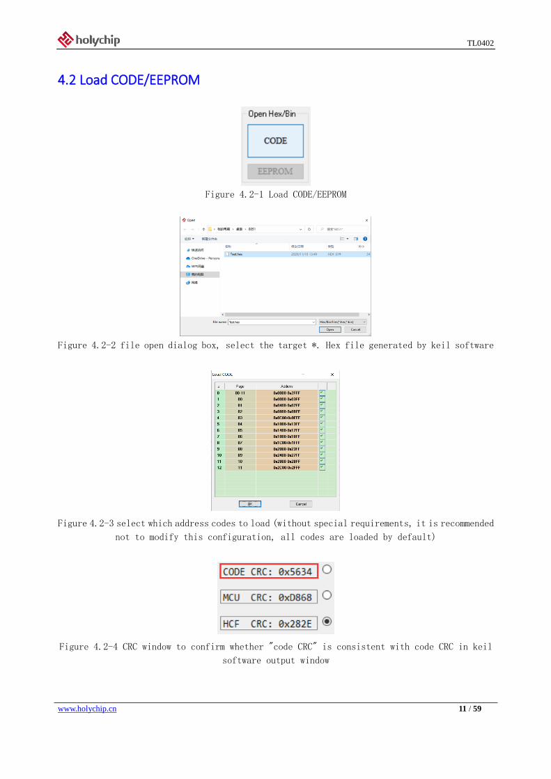
4.2 Load CODE/EEPROM
Figure 4.2-1 Load CODE/EEPROM
Figure 4.2-2 file open dialog box, select the target *. Hex file generated by keil software
Figure 4.2-3 select which address codes to load (without special requirements, it is recommended
not to modify this configuration, all codes are loaded by default)
Figure 4.2-4 CRC window to confirm whether "code CRC" is consistent with code CRC in keil
software output window
TL0402
www.holychip.cn 12 / 59
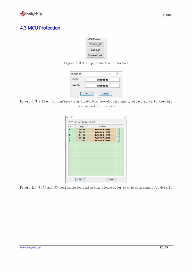
4.3 MCU Protection
Figure 4.3-1 chip protection interface
Figure 4.3-2 flash_SC configuration dialog box, hexadecimal input, please refer to the chip
data manual for details
Figure 4.3-3 IAP and ICP configuration dialog box, please refer to chip data manual for details
TL0402
www.holychip.cn 13 / 59
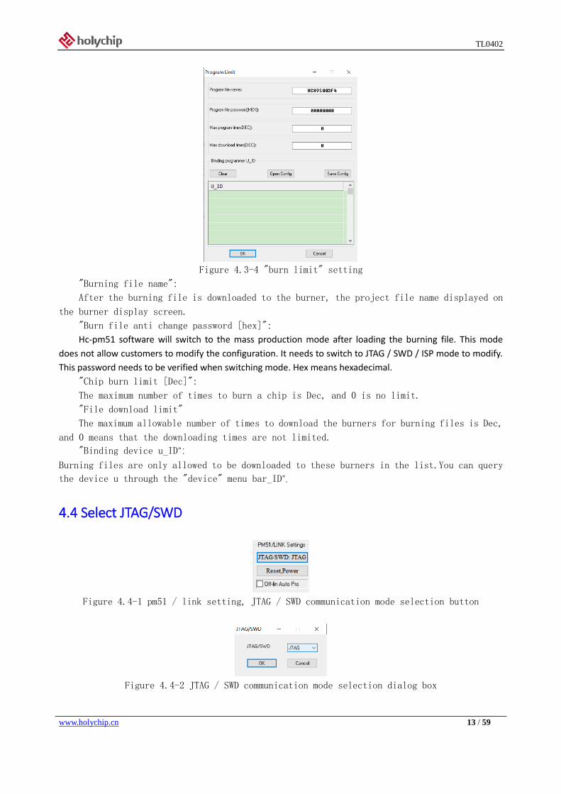
Figure 4.3-4 "burn limit" setting
"Burning file name":
After the burning file is downloaded to the burner, the project file name displayed on
the burner display screen.
"Burn file anti change password [hex]":
Hc-pm51 software will switch to the mass production mode after loading the burning file. This mode
does not allow customers to modify the configuration. It needs to switch to JTAG / SWD / ISP mode to modify.
This password needs to be verified when switching mode. Hex means hexadecimal.
"Chip burn limit [Dec]":
The maximum number of times to burn a chip is Dec, and 0 is no limit.
"File download limit"
The maximum allowable number of times to download the burners for burning files is Dec,
and 0 means that the downloading times are not limited.
"Binding device u_ID”:
Burning files are only allowed to be downloaded to these burners in the list.You can query
the device u through the "device" menu bar_ID”.
4.4 Select JTAG/SWD
Figure 4.4-1 pm51 / link setting, JTAG / SWD communication mode selection button
Figure 4.4-2 JTAG / SWD communication mode selection dialog box
TL0402
www.holychip.cn 14 / 59
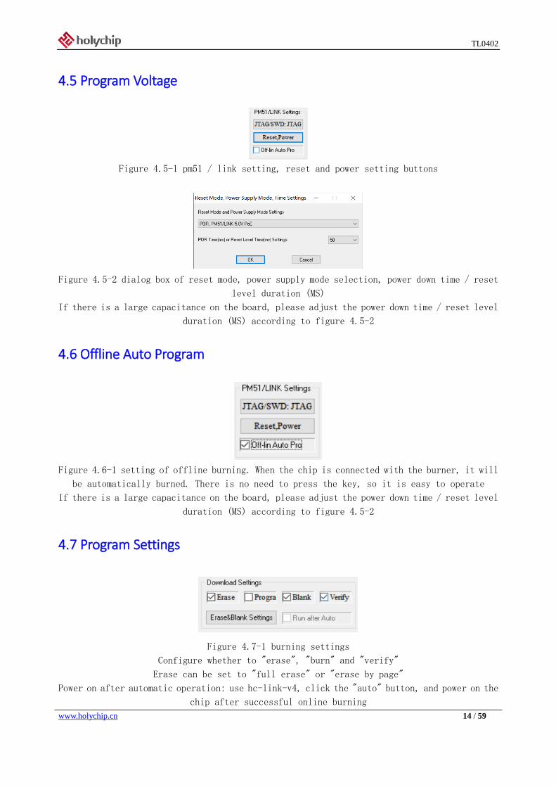
4.5 Program Voltage
Figure 4.5-1 pm51 / link setting, reset and power setting buttons
Figure 4.5-2 dialog box of reset mode, power supply mode selection, power down time / reset
level duration (MS)
If there is a large capacitance on the board, please adjust the power down time / reset level
duration (MS) according to figure 4.5-2
4.6 Offline Auto Program
Figure 4.6-1 setting of offline burning. When the chip is connected with the burner, it will
be automatically burned. There is no need to press the key, so it is easy to operate
If there is a large capacitance on the board, please adjust the power down time / reset level
duration (MS) according to figure 4.5-2
4.7 Program Settings
Figure 4.7-1 burning settings
Configure whether to "erase", "burn" and "verify"
Erase can be set to "full erase" or "erase by page"
Power on after automatic operation: use hc-link-v4, click the "auto" button, and power on the
chip after successful online burning

TL0402
www.holychip.cn 15 / 59
Figure 4.7-2 setting of erasing blank page
4.8 Save Program File
Figure 4.8-1 "save HCF" button in main interface
Figure 4.8-2 save file dialog box, select the save path and click the "save (s)" button
to save the burned file to the local disk
4.9 Download And Program
Please refer to "3.2 download burning file", "3.3 manual burning", "3.4 read code CRC",
"3.5 machine burning".
TL0402
www.holychip.cn 16 / 59
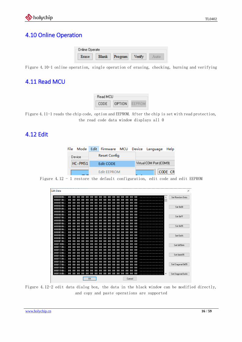
4.10 Online Operation
Figure 4.10-1 online operation, single operation of erasing, checking, burning and verifying
4.11 Read MCU
Figure 4.11-1 reads the chip code, option and EEPROM. After the chip is set with read protection,
the read code data window displays all 0
4.12 Edit
Figure 4.12 - 1 restore the default configuration, edit code and edit EEPROM
Figure 4.12-2 edit data dialog box, the data in the black window can be modified directly,
and copy and paste operations are supported
TL0402
www.holychip.cn 17 / 59
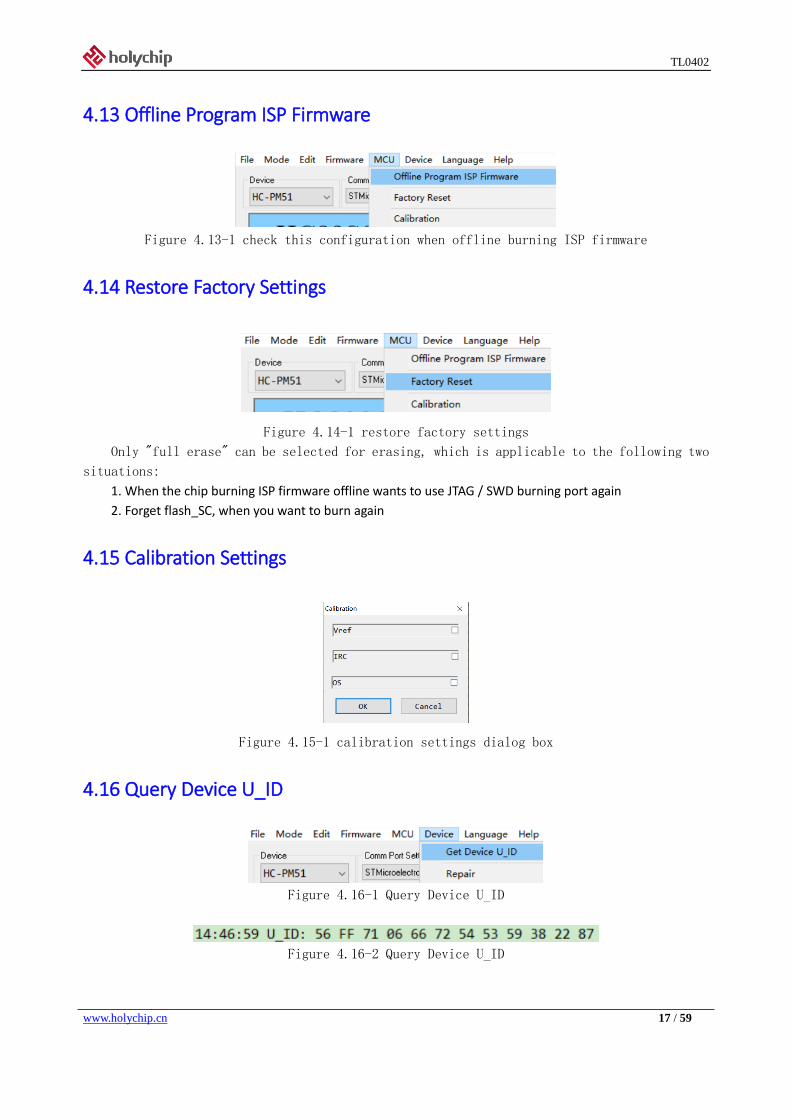
4.13 Offline Program ISP Firmware
Figure 4.13-1 check this configuration when offline burning ISP firmware
4.14 Restore Factory Settings
Figure 4.14-1 restore factory settings
Only "full erase" can be selected for erasing, which is applicable to the following two
situations:
1. When the chip burning ISP firmware offline wants to use JTAG / SWD burning port again
2. Forget flash_SC, when you want to burn again
4.15 Calibration Settings
Figure 4.15-1 calibration settings dialog box
4.16 Query Device U_ID
Figure 4.16-1 Query Device U_ID
Figure 4.16-2 Query Device U_ID
TL0402
www.holychip.cn 18 / 59
5 Software And Firmware Update
5.1 Software Update
Each time the upper computer software is opened, it will automatically connect to the
Xinsheng official website. If the official website software is updated, the upper computer
software will automatically pop up the software update prompt window, and the user can go to
the Xinsheng official website(http://www.holychip.cn)Download the latest software.
5.2 Firmware Update
When downloading burning files in 3.2, the upper computer software will automatically check
whether the firmware of the lower computer is the latest version. If the firmware does not
match, the upper computer software will prompt the user to update the firmware.
Before firmware update, please connect the USB of hc-pm51-v5 to the computer. Refer to
figure 3.2-1 to check whether the device port is correctly selected.
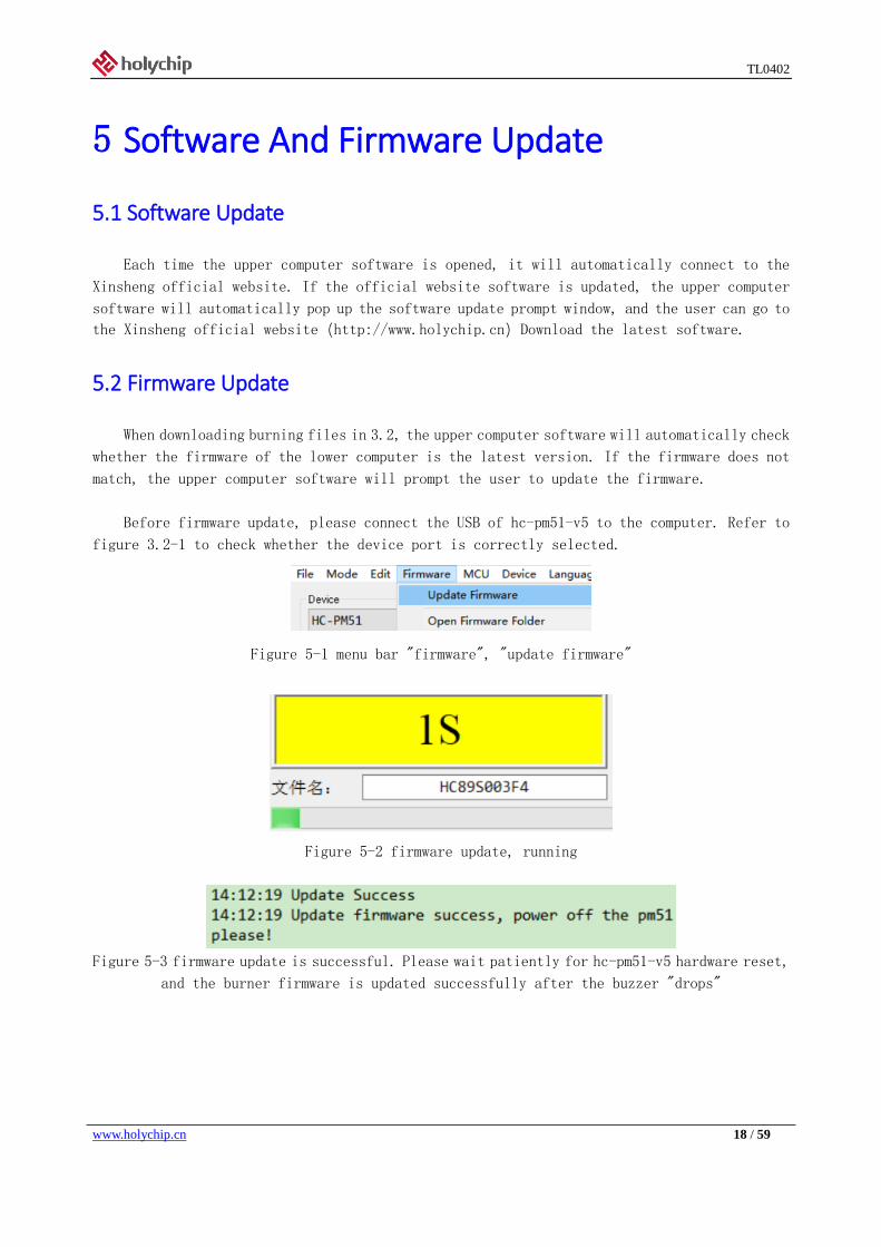
Figure 5-1 menu bar "firmware", "update firmware"
Figure 5-2 firmware update, running
Figure 5-3 firmware update is successful. Please wait patiently for hc-pm51-v5 hardware reset,
and the burner firmware is updated successfully after the buzzer "drops"
TL0402
www.holychip.cn 19 / 59
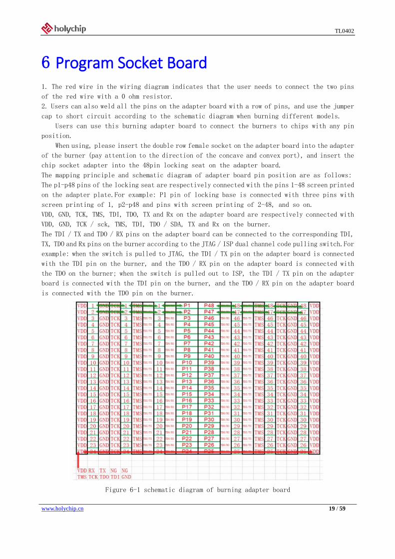
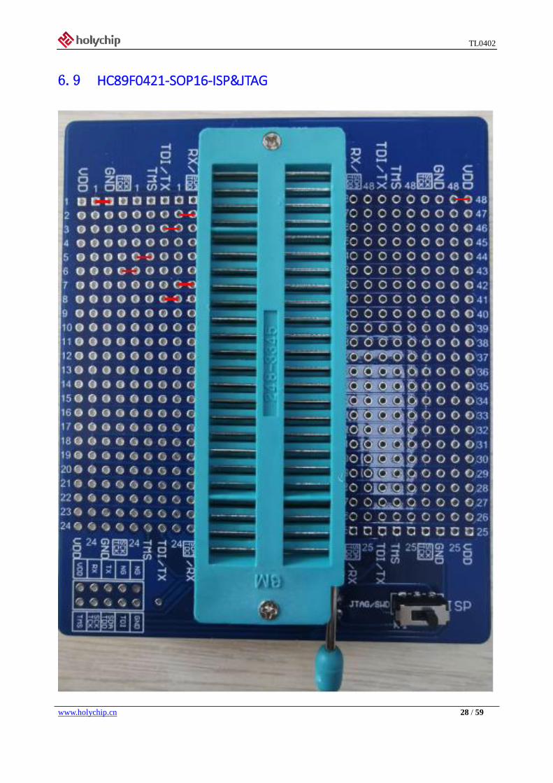
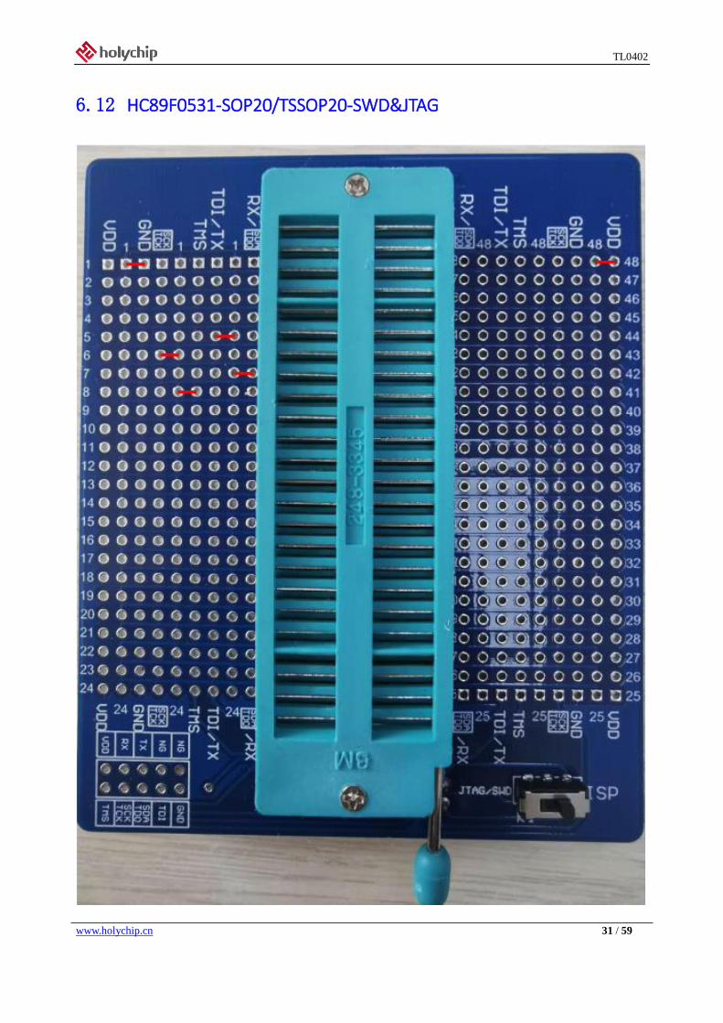
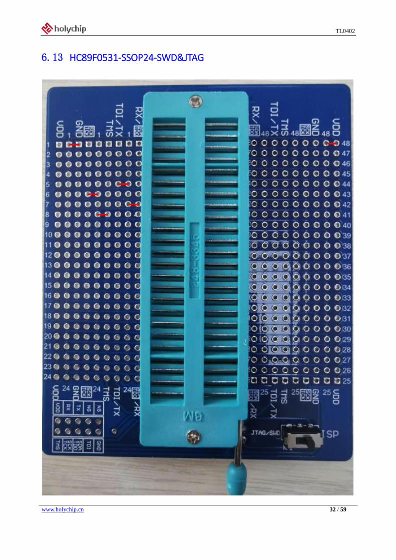
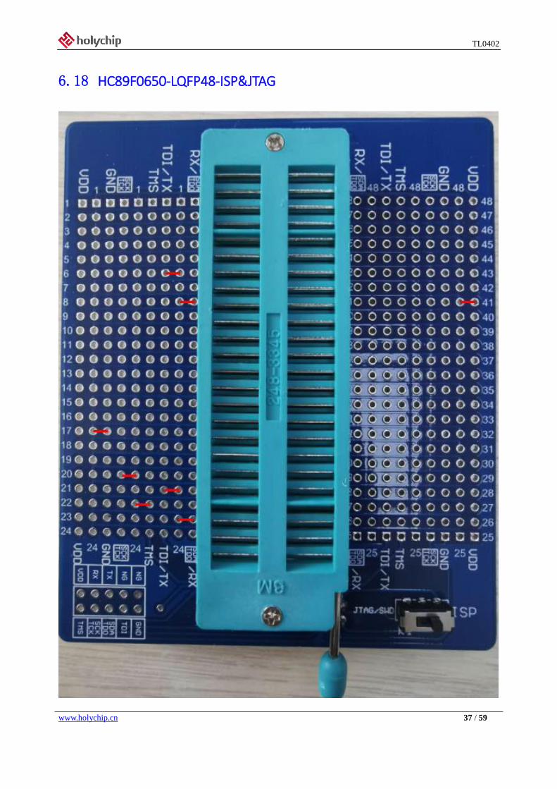
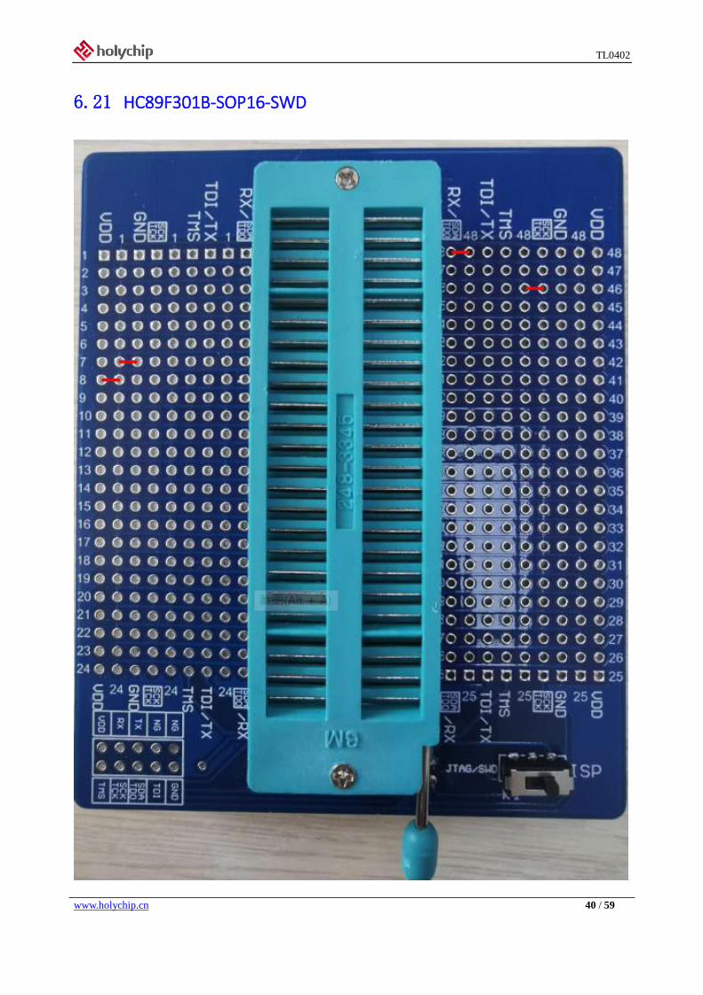
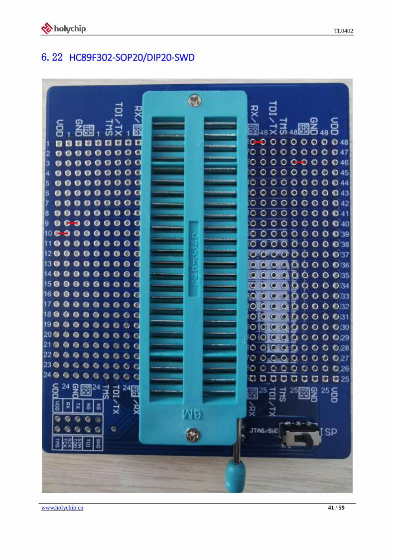
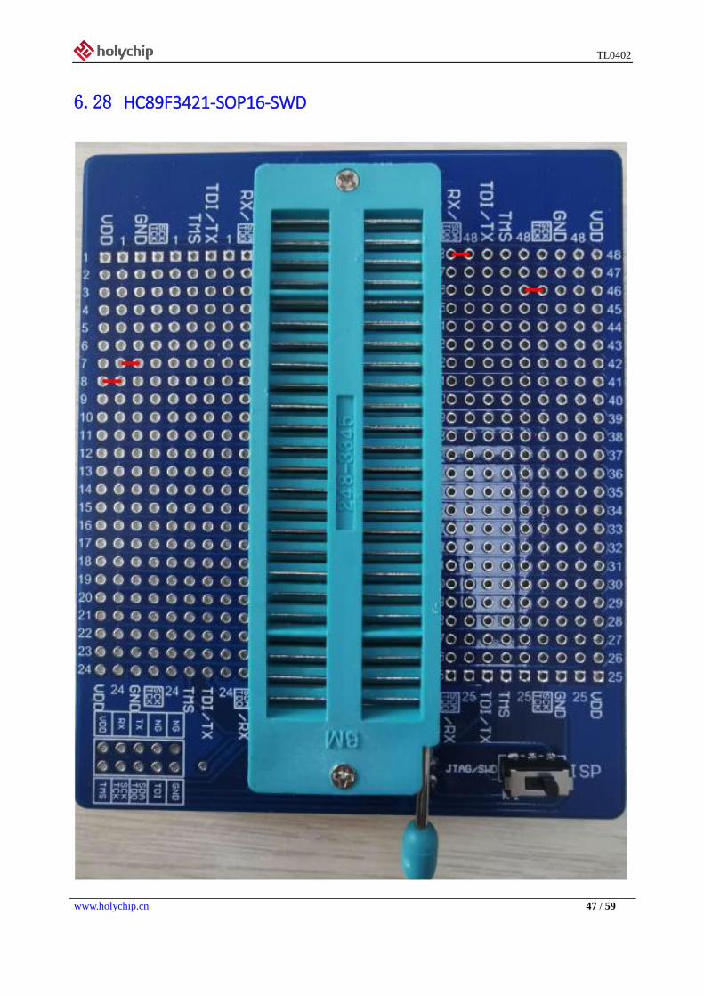
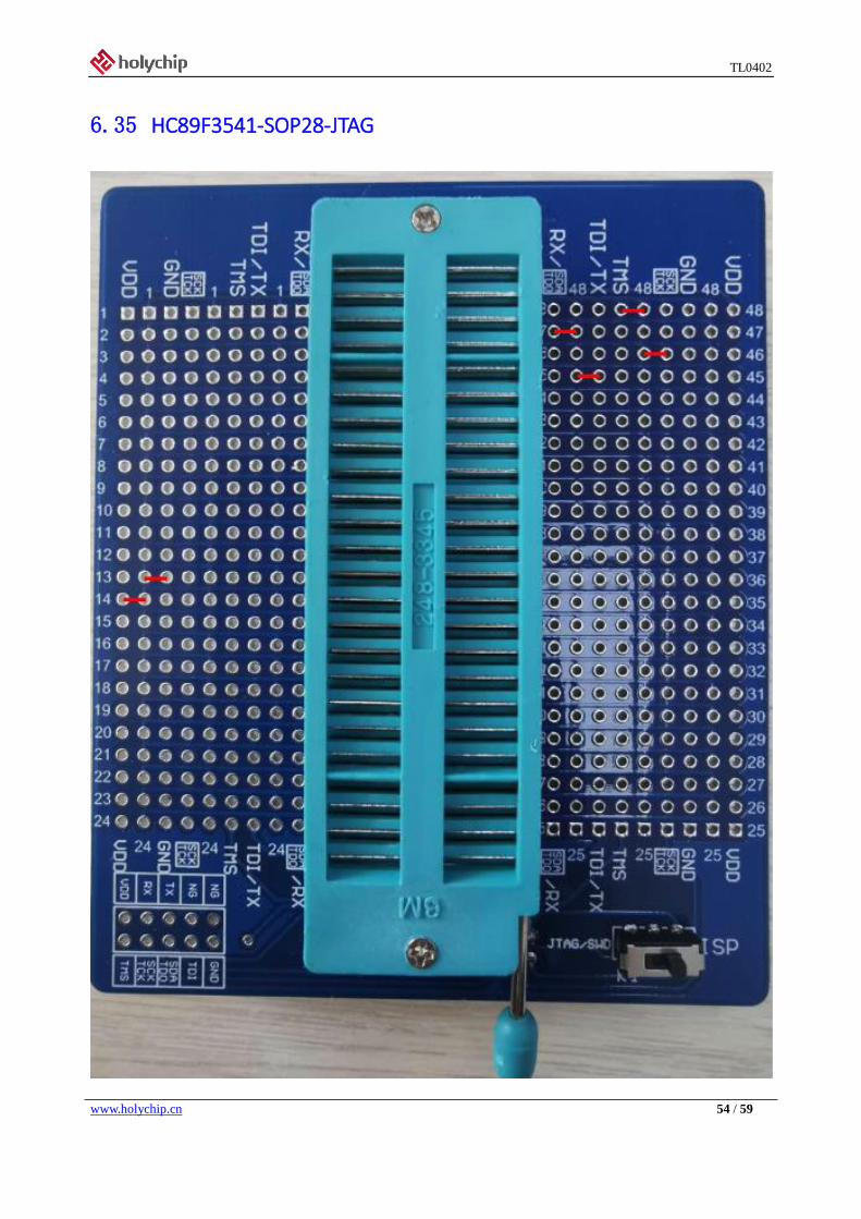
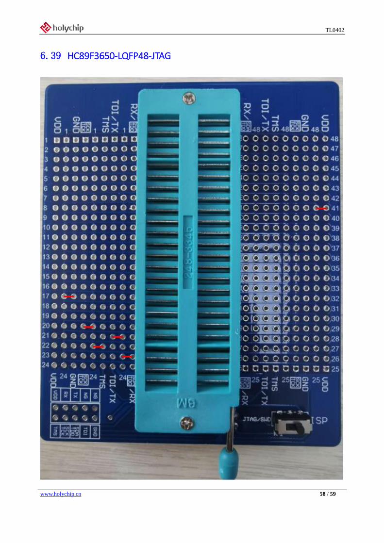
6 Program Socket Board 1. The red wire in the wiring diagram indicates that the user needs to connect the two pins
of the red wire with a 0 ohm resistor.
2. Users can also weld all the pins on the adapter board with a row of pins, and use the jumper
cap to short circuit according to the schematic diagram when burning different models.
Users can use this burning adapter board to connect the burners to chips with any pin
position.
When using, please insert the double row female socket on the adapter board into the adapter
of the burner (pay attention to the direction of the concave and convex port), and insert the
chip socket adapter into the 48pin locking seat on the adapter board.
The mapping principle and schematic diagram of adapter board pin position are as follows:
The p1-p48 pins of the locking seat are respectively connected with the pins 1-48 screen printed
on the adapter plate.For example: P1 pin of locking base is connected with three pins with
screen printing of 1, p2-p48 and pins with screen printing of 2-48, and so on.
VDD, GND, TCK, TMS, TDI, TDO, TX and Rx on the adapter board are respectively connected with
VDD, GND, TCK / sck, TMS, TDI, TDO / SDA, TX and Rx on the burner.
The TDI / TX and TDO / RX pins on the adapter board can be connected to the corresponding TDI,
TX, TDO and Rx pins on the burner according to the JTAG / ISP dual channel code pulling switch.For
example: when the switch is pulled to JTAG, the TDI / TX pin on the adapter board is connected
with the TDI pin on the burner, and the TDO / RX pin on the adapter board is connected with
the TDO on the burner; when the switch is pulled out to ISP, the TDI / TX pin on the adapter
board is connected with the TDI pin on the burner, and the TDO / RX pin on the adapter board
is connected with the TDO pin on the burner.
Figure 6-1 schematic diagram of burning adapter board

TL0402
www.holychip.cn 20 / 59
6.1 HC89S001P-SOP8-ISP

TL0402
www.holychip.cn 21 / 59
6.2 HC89S003F4-TSSOP20-ISP&JTAG

TL0402
www.holychip.cn 22 / 59
6.3 HC89S003F4-QFN20-ISP&JTAG
TL0402
www.holychip.cn 23 / 59
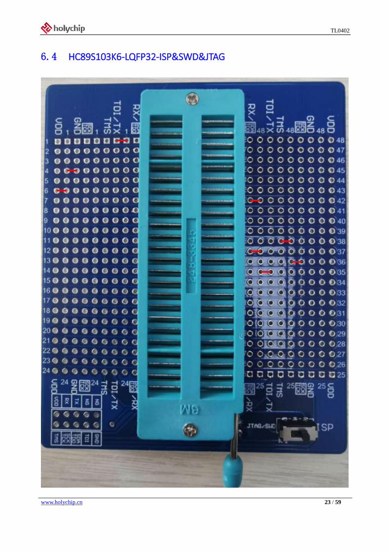
6.4 HC89S103K6-LQFP32-ISP&SWD&JTAG

TL0402
www.holychip.cn 24 / 59
6.5 HC89S105K8-LQFP32-ISP&JTAG
TL0402
www.holychip.cn 25 / 59
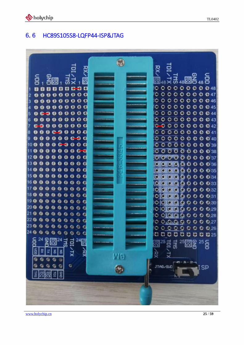
6.6 HC89S105S8-LQFP44-ISP&JTAG

TL0402
www.holychip.cn 26 / 59
6.7 HC89S105C8-LQFP48-ISP&JTAG

TL0402
www.holychip.cn 27 / 59
6.8 HC89F0411P-SOP8-ISP
TL0402
www.holychip.cn 28 / 59
6.9 HC89F0421-SOP16-ISP&JTAG

TL0402
www.holychip.cn 29 / 59
6.10 HC89F0431-SOP20/TSSOP20-ISP&JTAG

TL0402
www.holychip.cn 30 / 59
6.11 HC89F0431-QFN20-JTAG
TL0402
www.holychip.cn 31 / 59
6.12 HC89F0531-SOP20/TSSOP20-SWD&JTAG
TL0402
www.holychip.cn 32 / 59
6.13 HC89F0531-SSOP24-SWD&JTAG

TL0402
www.holychip.cn 33 / 59
6.14 HC89F0531-QFN24-SWD&JTAG

TL0402
www.holychip.cn 34 / 59
6.15 HC89F0541-SOP28/SSOP28-SWD&JTAG

TL0402
www.holychip.cn 35 / 59
6.16 HC89F0541-LQFP32/QFN32-SWD&JTAG

TL0402
www.holychip.cn 36 / 59
6.17 HC89F0650-LQFP44-ISP&JTAG
TL0402
www.holychip.cn 37 / 59
6.18 HC89F0650-LQFP48-ISP&JTAG

TL0402
www.holychip.cn 38 / 59
6.19 HC8M602-SOP16-SWD

TL0402
www.holychip.cn 39 / 59
6.20 HC89F301-SOP16-SWD
TL0402
www.holychip.cn 40 / 59
6.21 HC89F301B-SOP16-SWD
TL0402
www.holychip.cn 41 / 59
6.22 HC89F302-SOP20/DIP20-SWD

TL0402
www.holychip.cn 42 / 59
6.23 HC89F302-SOP24-SWD

TL0402
www.holychip.cn 43 / 59
6.24 HC89F302B-SOP20/DIP20-SWD

TL0402
www.holychip.cn 44 / 59
6.25 HC89F302B-SOP24-SWD

TL0402
www.holychip.cn 45 / 59
6.26 HC89F303-SOP28-SWD

TL0402
www.holychip.cn 46 / 59
6.27 HC89F303B-SOP28-SWD
TL0402
www.holychip.cn 47 / 59
6.28 HC89F3421-SOP16-SWD

TL0402
www.holychip.cn 48 / 59
6.29 HC89F3421-SOP16-JTAG

TL0402
www.holychip.cn 49 / 59
6.30 HC89F3531-SOP20/DIP20-SWD

TL0402
www.holychip.cn 50 / 59
6.31 HC89F3531-SOP20/DIP20-JTAG

TL0402
www.holychip.cn 51 / 59
6.32 HC89F3531-SOP24-SWD

TL0402
www.holychip.cn 52 / 59
6.33 HC89F3531-SOP24-JTAG

TL0402
www.holychip.cn 53 / 59
6.34 HC89F3541-SOP28-SWD
TL0402
www.holychip.cn 54 / 59
6.35 HC89F3541-SOP28-JTAG

TL0402
www.holychip.cn 55 / 59
6.36 HC89F3541-LQFP32-SWD

TL0402
www.holychip.cn 56 / 59
6.37 HC89F3541-LQFP32-JTAG

TL0402
www.holychip.cn 57 / 59
6.38 HC89F3650-LQFP44-JTAG
TL0402
www.holychip.cn 58 / 59
6.39 HC89F3650-LQFP48-JTAG
TL0402
www.holychip.cn 59 / 59
7 Version Description Version Date Describe
Ver1.00 2020/11/6 First edition
IMPORTANT NOTICE – PLEASE READ CAREFULLY
Holychip reserves the right to make change without further notice to any products herein to improve
reliability, function or design. Holychip does not assume any liability arising out of the application or use of
any product or circuit described herein; neither does it convey any license under its patent rights nor the
rights of others. Holychip products are not designed, intended, or authorized for us as components in system
intended, for surgical implant into the body, or other applications intended to support or sustain life, or for
any other application in which the failure of the Holychip product could create a situation where personal
injury or death may occur. Should Buyer purchase or use Holychip products for any such unintended or
unauthorized application. Buyer shall indemnify and hold Holychip and its officers, employees, subsidiaries,
affiliates and distributors harmless against all claims, cost, damages, and expenses, and reasonable attorney
fees arising out of, directly or indirectly, any claim of personal injury or death associated with such
unintended or unauthorized use even if such claim alleges that Holychip was negligent regarding the design
or manufacture of the part.
Holychip