
8-Channel HD Compatible Audio Processor with … · Digital Audio Processor (DAP) 10ch input ......
116
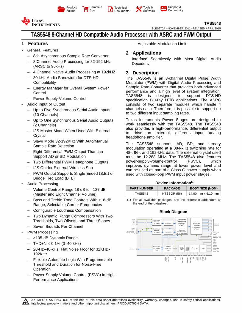
Serial Audio Receiver 2x Stereo Serial Audio Receiver 2x Stereo Serial Audio Transciever Stereo 4ch ASRC 4ch ASRC Fixed Flow Digital Audio Processor (DAP) 10ch input 8ch Processor 8ch Output Mixer Clocks (Osc, PLL etc) 12.288 8ch PWM Generator + Headphone (PWM) Bypass MCU I2C Control Power Supply Volume Control (PSVC) Energy Manager (EMO) Power SDA SCL SDOUT/SDIN5 SDIN1 SDIN2 SCLK LRCLK SDIN2-1 SDIN2-2 SCLKO /SCLKIN_2 LRCLKO / LRCKIN_2 OSCRES PLL_FLTM PLL_FLTP MCLK EMO1 ASEL_EMO2 PSVC/MCLKO VR_DIG VR_PWM VR_ANA AVDD AVDD_PWM AVSS AVSS_PWM DVDD1 DVDD2 DVSS1 DVSS2 /PDN PWM_HPM_L&R PWM_HPP_L&R /BKND_ERR PWM_x_1 through 8 ASEL_EMO2 VALID /MUTE TEST RESET /HP_SEL Product Folder Sample & Buy Technical Documents Tools & Software Support & Community TAS5548 SLES270A – NOVEMBER 2012 – REVISED APRIL 2015 TAS5548 8-Channel HD Compatible Audio Processor with ASRC and PWM Output 1 Features – Adjustable Modulation Limit 1• General Features 2 Applications – 8ch Asynchronous Sample Rate Converter Interface Seamlessly with Most Digital Audio – 8 Channel Audio Processing for 32-192 kHz Decoders (ARSC to 96kHz) – 4 Channel Native Audio Processing at 192kHZ 3 Description – 30 kHz Audio Bandwidth for DTS-HD The TAS5548 is an 8-channel Digital Pulse Width Compatibility Modulator (PWM) with Digital Audio Processing and Sample Rate Converter that provides both advanced – Energy Manager for Overall System Power performance and a high level of system integration. Control TAS5548 is designed to support DTS-HD – Power Supply Volume Control specification Blu-ray HTiB applications. The ASRC • Audio Input or Output consists of two separate modules which handle 4 channels each. Therefore, it is possible to support up – Up to Five Synchronous Serial Audio Inputs to two different input sampling rates. (10 Channels) Texas Instruments Power Stages are designed to – Up to One Synchronous Serial Audio Outputs work seamlessly with the TAS5548. The TAS5548 (2 Channels) also provides a high-performance, differential output – I2S Master Mode When Used With External to drive an external, differential-input, analog Crystal headphone amplifier. – Slave Mode 32-192KHz With Auto/Manual The TAS5548 supports AD, BD, and ternary Sample Rate Detection modulation operating at a 384-kHz switching rate for – Eight Differential PWM Output That can 48-, 96-, and 192-kHz data. The external crystal used Support AD or BD Modulation must be 12.288 MHz. The TAS5548 also features power-supply-volume-control (PSVC), which – Two Differential PWM Headphone Outputs improves dynamic range at lower power level and – I2S Out for External Wireless Sub can be used as part of a Class G power supply when – PWM Output Supports Single Ended (S.E.) or used with closed-loop PWM input power stages. Bridge Tied Load (BTL) Device Information (1) • Audio Processing PART NUMBER PACKAGE BODY SIZE (NOM) – Volume Control Range 18 dB to –127 dB TAS5548 HTSSOP (56) 14.00 mm x 6.10 mm (Master and Eight Channel Volume) (1) For all available packages, see the orderable addendum at – Bass and Treble Tone Controls With ±18-dB the end of the datasheet. Range, Selectable Corner Frequencies – Configurable Loudness Compensation Block Diagram – Two Dynamic Range Compressors With Two Thresholds, Two Offsets, and Three Slopes – Seven Biquads Per Channel • PWM Processing – >105-dB Dynamic Range – THD+N < 0.1% (0–40 kHz) – 20-Hz–40-kHz, Flat Noise Floor for 32KHz - 192KHz – Flexible Automute Logic With Programmable Threshold and Duration for Noise-Free Operation – Power-Supply Volume Control (PSVC) in High- Performance Applications 1 An IMPORTANT NOTICE at the end of this data sheet addresses availability, warranty, changes, use in safety-critical applications, intellectual property matters and other important disclaimers. PRODUCTION DATA.
Transcript of 8-Channel HD Compatible Audio Processor with … · Digital Audio Processor (DAP) 10ch input ......
Serial Audio Receiver2x Stereo
Serial Audio Receiver2x Stereo
Serial Audio Transciever
Stereo
4ch ASRC
4ch ASRC
Fixed FlowDigital Audio
Processor (DAP)
10ch input8ch Processor
8ch Output Mixer
Clocks(Osc, PLL
etc)12.288
8ch PWM Generator+ Headphone
(PWM)Bypass
MCUI2C
Control
Power Supply Volume Control(PSVC)
Energy Manager (EMO)
Power
SD
A
SC
L
SDOUT/SDIN5
SDIN1
SDIN2
SCLK
LRCLK
SDIN2-1
SDIN2-2
SCLKO /SCLKIN_2
LRCLKO / LRCKIN_2
OS
CR
ES
PLL
_FLT
M
PLL
_FLT
P
MC
LK
EM
O1
AS
EL_
EM
O2
PS
VC
/MC
LKO
VR
_DIG
VR
_PW
M
VR
_AN
A
AV
DD
AVDD_PWM
AVSS
AVSS_PWM
DVDD1
DVDD2
DVSS1
DVSS2
/PDN
PWM_HPM_L&R
PWM_HPP_L&R
/BKND_ERR
PWM_x_1 through 8
AS
EL_
EM
O2
VALID
/MUTE
TE
ST
RE
SE
T
/HP
_SE
L
Product
Folder
Sample &Buy
Technical
Documents
Tools &
Software
Support &Community
TAS5548SLES270A –NOVEMBER 2012–REVISED APRIL 2015
TAS5548 8-Channel HD Compatible Audio Processor with ASRC and PWM Output1 Features – Adjustable Modulation Limit1• General Features 2 Applications
– 8ch Asynchronous Sample Rate ConverterInterface Seamlessly with Most Digital Audio
– 8 Channel Audio Processing for 32-192 kHz Decoders(ARSC to 96kHz)
– 4 Channel Native Audio Processing at 192kHZ 3 Description– 30 kHz Audio Bandwidth for DTS-HD The TAS5548 is an 8-channel Digital Pulse Width
Compatibility Modulator (PWM) with Digital Audio Processing andSample Rate Converter that provides both advanced– Energy Manager for Overall System Powerperformance and a high level of system integration.ControlTAS5548 is designed to support DTS-HD
– Power Supply Volume Control specification Blu-ray HTiB applications. The ASRC• Audio Input or Output consists of two separate modules which handle 4
channels each. Therefore, it is possible to support up– Up to Five Synchronous Serial Audio Inputsto two different input sampling rates.(10 Channels)Texas Instruments Power Stages are designed to– Up to One Synchronous Serial Audio Outputswork seamlessly with the TAS5548. The TAS5548(2 Channels)also provides a high-performance, differential output– I2S Master Mode When Used With External to drive an external, differential-input, analog
Crystal headphone amplifier.– Slave Mode 32-192KHz With Auto/Manual The TAS5548 supports AD, BD, and ternarySample Rate Detection modulation operating at a 384-kHz switching rate for– Eight Differential PWM Output That can 48-, 96-, and 192-kHz data. The external crystal used
Support AD or BD Modulation must be 12.288 MHz. The TAS5548 also featurespower-supply-volume-control (PSVC), which– Two Differential PWM Headphone Outputsimproves dynamic range at lower power level and– I2S Out for External Wireless Sub can be used as part of a Class G power supply when
– PWM Output Supports Single Ended (S.E.) or used with closed-loop PWM input power stages.Bridge Tied Load (BTL)
Device Information(1)• Audio ProcessingPART NUMBER PACKAGE BODY SIZE (NOM)– Volume Control Range 18 dB to –127 dB
TAS5548 HTSSOP (56) 14.00 mm x 6.10 mm(Master and Eight Channel Volume)(1) For all available packages, see the orderable addendum at– Bass and Treble Tone Controls With ±18-dB
the end of the datasheet.Range, Selectable Corner Frequencies– Configurable Loudness Compensation Block Diagram– Two Dynamic Range Compressors With Two
Thresholds, Two Offsets, and Three Slopes– Seven Biquads Per Channel
• PWM Processing– >105-dB Dynamic Range– THD+N < 0.1% (0–40 kHz)– 20-Hz–40-kHz, Flat Noise Floor for 32KHz -
192KHz– Flexible Automute Logic With Programmable
Threshold and Duration for Noise-FreeOperation
– Power-Supply Volume Control (PSVC) in High-Performance Applications
1
An IMPORTANT NOTICE at the end of this data sheet addresses availability, warranty, changes, use in safety-critical applications,intellectual property matters and other important disclaimers. PRODUCTION DATA.
TAS5548SLES270A –NOVEMBER 2012–REVISED APRIL 2015 www.ti.com
Table of Contents7.1 Overview ................................................................. 141 Features .................................................................. 17.2 Functional Block Diagram ....................................... 142 Applications ........................................................... 17.3 Feature Description................................................. 163 Description ............................................................. 17.4 Device Functional Modes........................................ 254 Revision History..................................................... 27.5 Programming........................................................... 485 Pin Configuration and Functions ......................... 37.6 Register Maps ......................................................... 536 Specifications......................................................... 6 8 Application and Implementation ........................ 956.1 Absolute Maximum Ratings ..................................... 68.1 Application Information............................................ 956.2 ESD Ratings.............................................................. 68.2 Typical Applications ................................................ 956.3 Recommended Operating Conditions....................... 68.3 Do’s and Don’ts..................................................... 1026.4 Thermal Information .................................................. 68.4 Initialization Set Up ............................................... 1026.5 Electrical Characteristics........................................... 7
9 Power Supply Recommendations .................... 1036.6 Dynamic Performance ............................................. 79.1 Power Supply ........................................................ 1036.7 SRC Performance ..................................................... 79.2 Energy Manager.................................................... 1036.8 Timing I2C Serial Control Port Operation.................. 89.3 Programming Energy Manager............................. 1046.9 Reset Timing (RESET) ............................................. 8
10 Layout................................................................. 1056.10 Power-Down (PDN) Timing..................................... 810.1 Layout Guidelines ............................................... 1056.11 Back-End Error (BKND_ERR) ............................... 810.2 Layout Example .................................................. 1066.12 Mute Timing (MUTE).............................................. 9
11 Device and Documentation Support ............... 1086.13 Headphone Select (HP_SEL) ................................ 911.1 Documentation Support ...................................... 1086.14 Switching Characteristics - Clock Signals............... 911.2 Trademarks ......................................................... 1086.15 Switching Characteristics - Serial Audio Port ....... 911.3 Electrostatic Discharge Caution.......................... 1086.16 Volume Control .................................................... 1011.4 Glossary .............................................................. 1086.17 Typical Characteristics .......................................... 13
12 Mechanical, Packaging, and Orderable7 Detailed Description ............................................ 14Information ......................................................... 108
4 Revision HistoryNOTE: Page numbers for previous revisions may differ from page numbers in the current version.
Changes from Original (November 2012) to Revision A Page
• Added ESD Ratings table, Feature Description section, Device Functional Modes, Application and Implementationsection, Power Supply Recommendations section, Layout section, Device and Documentation Support section, andMechanical, Packaging, and Orderable Information section. ................................................................................................. 1
• Added the Thermal Information table ..................................................................................................................................... 6• Updated Figure 23 ............................................................................................................................................................... 29• Updated Figure 24................................................................................................................................................................ 30• Updated Table 12 ................................................................................................................................................................. 46
2 Submit Documentation Feedback Copyright © 2012–2015, Texas Instruments Incorporated
Product Folder Links: TAS5548
PWM_HPM_L 1
2
3
4
5
6
7
PWM_HPP_R
AVSS
PLL_FLTM
PLL_FLTP
SDIN1
VR_ANA
SDIN2
AVDD
ASEL_EMO2
SCLK
SDIN2_1 (SDIN3)
XTALI
XTALO
DVSS2
DVDD2
EMO1
RESET
HP_SEL
PDN
MUTE
VR_DIG
LRCLK
SDA
SCL
PWM_HPP_L
PWM_HPM_R
8
9
10
11
12
13
14
15
16
17
18
19
20
21
22
23
24
25
26
27
28 29
30
31
32
33
34
35
36
37
38
39
40
41
42
43
44
45
46
47
48
49
50
51
52
53
54
55
56 PWM_P_6
PWM_M_6
PWM_P_5
PWM_M_5
VR_PWM
AVSS_PWM
AVDD_PWM
PWM_P_8
PWM_M_8
PWM_P_7
PWM_M_7
PWM_P_4
PWM_M_4
PWM_P_3
PWM_M_3
PWM_P_2
PWM_M_2
PWM_P_1
VALID
DVDD1
PWM_M_1
DVSS1
BKND_ERR
PSVC/MLCK
TEST
LRCLKO (LRCK#2)
SCLKO (SCLK#2)
SDOUT (SDIN5)
SDIN2_2 (SDIN4)
TAS5548www.ti.com SLES270A –NOVEMBER 2012–REVISED APRIL 2015
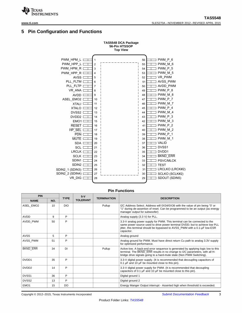
5 Pin Configuration and Functions
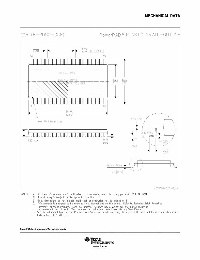
TAS5548 DCA Package56-Pin HTSSOP
Top View
Pin FunctionsPIN 5-VTYPE TERMINATION DESCRIPTIONTOLERANTNAME NO.
ASEL_EMO2 10 DIO Pullup I2C Address Select. Address will 0X34/0X36 with the value of pin being "0' or"1" during de-assertion of reset. Can be programmed to be an output (as energymanager output for subwoofer)
AVDD 9 P Analog supply (3.3 V) for PLL.
AVDD_PWM 50 P 3.3-V analog power supply for PWM. This terminal can be connected to thesame power source used to drive power terminal DVDD; but to achieve low PLLjitter, this terminal should be bypassed to AVSS_PWM with a 0.1-μF low-ESRcapacitor.
AVSS 5 P Analog ground
AVSS_PWM 51 P Analog ground for PWM. Must have direct return Cu path to analog 3.3V supplyfor optimized performance.
BKND_ERR 34 DI Pullup Active-low. A back-end error sequence is generated by applying logic low to thisterminal. The BKND_ERR results in no change to I2C parameters, with all H-bridge drive signals going to a hard-mute state (Non PWM Switching).
DVDD1 35 P 3.3-V digital power supply. (It is recommended that decoupling capacitors of0.1 μF and 10 μF be mounted close to this pin).
DVDD2 14 P 3.3-V digital power supply for PWM. (It is recommended that decouplingcapacitors of 0.1 μF and 10 μF be mounted close to this pin).
DVSS1 36 P Digital ground 1
DVSS2 13 P Digital ground 2
EMO1 15 DO Energy Manger Output interrupt - Asserted high when threshold is exceeded.
Copyright © 2012–2015, Texas Instruments Incorporated Submit Documentation Feedback 3
Product Folder Links: TAS5548
TAS5548SLES270A –NOVEMBER 2012–REVISED APRIL 2015 www.ti.com
Pin Functions (continued)PIN 5-VTYPE TERMINATION DESCRIPTIONTOLERANTNAME NO.
HP_SEL 17 DI 5 V Pullup Headphone/speaker selector. When a logic low is applied, the headphone isselected (speakers are off). When a logic high is applied, speakers are selected(headphone is off).
LRCLK 22 DI 5 V Pulldown Serial-audio data left/right clock (sampling-rate clock)
LRCLKO / 31 DIO 5V Pulldown LRCLK for I2S OUT. Can also be used as LRCKIN_2 (I2S Input for SDIN2_xLRCKIN_2 and SRC Bank 2)
XTALI 11 DI 1.8 V XTAL input. Connect to external 12.288 MHz XTAL
MUTE 19 DI 5 V Pullup Soft mute of outputs, active-low (muted signal = a logic low, normal operation =a logic high). The mute control provides a noiseless volume ramp to silence.Releasing mute provides a noiseless ramp to previous volume.
XTALO 12 DO XTAL input. Connect to external 12.288 MHz XTAL
PDN 18 DI 5 V Pullup Power down, active-low. PDN powers down all logic and stops all clockswhenever a logic low is applied. The I2C parameters are preserved through apower-down cycle, as long as RESET is not active.
PLL_FLTM 6 AIO PLL negative filter.
PLL_FLTP 7 AIO PLL positive filter.
PSVC/MCLKO 33 DO Power-supply volume control PWM output or MCKO for external ADC (SDIN5Source)
PWM_HPM_L 1 DO PWM left-channel headphone (differential –)
PWM_HPM_R 3 DO PWM right-channel headphone (differential –)
PWM_HPP_L 2 DO PWM left-channel headphone (differential +)
PWM_HPP_R 4 DO PWM right-channel headphone (differential +)
PWM_M_1 38 DO PWM 1 output (differential –)
PWM_M_2 40 DO PWM 2 output (differential –)
PWM_M_3 42 DO PWM 3 output (differential –)
PWM_M_4 44 DO PWM 4 output (differential –)
PWM_M_5 53 DO PWM 5 output (lineout L) (differential –)
PWM_M_6 55 DO PWM 6 output (lineout R) (differential –)
PWM_M_7 46 DO PWM 7 output (differential –)
PWM_M_8 48 DO PWM 8 output (differential –)
PWM_P_1 39 DO PWM 1 output (differential +)
PWM_P_2 41 DO PWM 2 output (differential +)
PWM_P_3 43 DO PWM 3 output (differential +)
PWM_P_4 45 DO PWM 4 output (differential +)
PWM_P_5 54 DO PWM 5 output (lineout L) (differential +)
PWM_P_6 56 DO PWM 6 output (lineout R) (differential +)
PWM_P_7 47 DO PWM 7 output (differential +)
PWM_P_8 49 DO PWM 8 output (differential +)
RESET 16 DI 5 V Pullup System reset input, active-low. A system reset is generated by applying a logiclow to this terminal. RESET is an asynchronous control signal that restores theTAS5548 to its default conditions, sets the valid output low, and places thePWM in the hard-mute state (Non PWM Switching). Master volume isimmediately set to full attenuation. On the release of RESET, if PDN is high, thesystem performs a 4- to 5-ms device initialization and sets the volume at mute.
SCL 21 DI 5 V I2C serial-control clock input/output
SCLK 23 DI 5 V Pulldown Serial-audio data clock (shift clock) input
SCLKO / 30 DIO 5V Pulldown Serial data clock out. I2S bit clock out. Can also be used as SCLKIN_2 (I2SSCLKIN_2 Input for SDIN2_x and SRC Bank 2)
SDA 20 DIO 5 V I2C serial-control data-interface input/output
SDIN1 24 DI 5 V Pulldown Serial-audio data bank 1 input 1 is one of the serial-data input ports and goesinto the 1st SRC Bank. Four discrete (stereo) data formats and is capable ofinputting data at 64 fS.
SDIN2 25 DI 5 V Pulldown Serial-audio data bank 1 input 2 is one of the serial-data input ports and goesinto the 1st SRC Bank. Four discrete (stereo) data formats and is capable ofinputting data at 64 fS.
4 Submit Documentation Feedback Copyright © 2012–2015, Texas Instruments Incorporated
Product Folder Links: TAS5548
TAS5548www.ti.com SLES270A –NOVEMBER 2012–REVISED APRIL 2015
Pin Functions (continued)PIN 5-VTYPE TERMINATION DESCRIPTIONTOLERANTNAME NO.
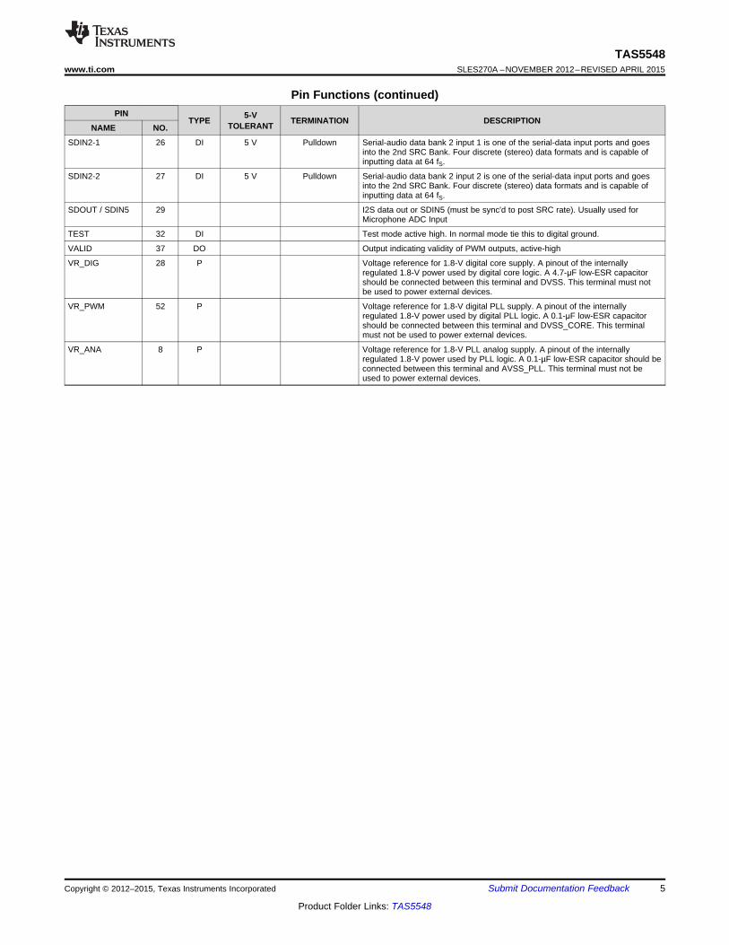
SDIN2-1 26 DI 5 V Pulldown Serial-audio data bank 2 input 1 is one of the serial-data input ports and goesinto the 2nd SRC Bank. Four discrete (stereo) data formats and is capable ofinputting data at 64 fS.
SDIN2-2 27 DI 5 V Pulldown Serial-audio data bank 2 input 2 is one of the serial-data input ports and goesinto the 2nd SRC Bank. Four discrete (stereo) data formats and is capable ofinputting data at 64 fS.
SDOUT / SDIN5 29 I2S data out or SDIN5 (must be sync'd to post SRC rate). Usually used forMicrophone ADC Input
TEST 32 DI Test mode active high. In normal mode tie this to digital ground.
VALID 37 DO Output indicating validity of PWM outputs, active-high
VR_DIG 28 P Voltage reference for 1.8-V digital core supply. A pinout of the internallyregulated 1.8-V power used by digital core logic. A 4.7-μF low-ESR capacitorshould be connected between this terminal and DVSS. This terminal must notbe used to power external devices.
VR_PWM 52 P Voltage reference for 1.8-V digital PLL supply. A pinout of the internallyregulated 1.8-V power used by digital PLL logic. A 0.1-μF low-ESR capacitorshould be connected between this terminal and DVSS_CORE. This terminalmust not be used to power external devices.
VR_ANA 8 P Voltage reference for 1.8-V PLL analog supply. A pinout of the internallyregulated 1.8-V power used by PLL logic. A 0.1-µF low-ESR capacitor should beconnected between this terminal and AVSS_PLL. This terminal must not beused to power external devices.
Copyright © 2012–2015, Texas Instruments Incorporated Submit Documentation Feedback 5
Product Folder Links: TAS5548
TAS5548SLES270A –NOVEMBER 2012–REVISED APRIL 2015 www.ti.com
6 Specifications
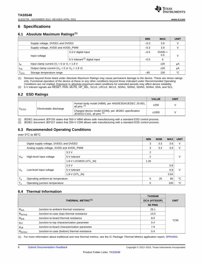
6.1 Absolute Maximum Ratings (1)
MIN MAX UNITSupply voltage, DVDD1 and DVDD2 –0.3 3.9 VSupply voltage, AVDD and AVDD_PWM –0.3 3.9 V
3.3-V digital input –0.5 DVDD +0.5Input voltage V
5-V tolerant (2) digital input –0.5 6IIK Input clamp current (VI < 0 or VI > 1.8 V ±20 μAIOK Output clamp current (VO < 0 or VO > 1.8 V) ±20 μATSTG Storage temperature range –65 150 °C
(1) Stresses beyond those listed under Absolute Maximum Ratings may cause permanent damage to the device. These are stress ratingsonly. Functional operation of the device at these or any other conditions beyond those indicated under Recommended OperatingConditions are not implied. Exposure to absolute-maximum-rated conditions for extended periods may affect device reliability.
(2) 5-V tolerant signals are RESET, PDN, MUTE, HP_SEL, SCLK, LRCLK, MCLK, SDIN1, SDIN2, SDIN3, SDIN4, SDA, and SCL.
6.2 ESD RatingsVALUE UNIT
Human body model (HBM), per ANSI/ESDA/JEDEC JS-001, ±250 Vall pins (1)V(ESD) Electrostatic discharge
Charged device model (CDM), per JEDEC specification ±1000 VJESD22-C101, all pins (2)
(1) JEDEC document JEP155 states that 500-V HBM allows safe manufacturing with a standard ESD control process.(2) JEDEC document JEP157 states that 250-V CDM allows safe manufacturing with a standard ESD control process.
6.3 Recommended Operating Conditionsover 0°C to 85°C
MIN NOM MAX UNITDigital supply voltage, DVDD1 and DVDD2 3 3.3 3.6 VAnalog supply voltage, AVDD and AVDD_PWM 3 3.3 3.6 V
3.3 V 2VIH High-level input voltage 5-V tolerant 2 V
1.8-V LVCMOS (XTL_IN) 1.263.3 V 0.8
VIL Low-level input voltage 5-V tolerant 0.8 V1.8-V (XTL_IN) 0.54
TA Operating ambient-air temperature 0 25 85 °CTJ Operating junction temperature 0 105 °C
6.4 Thermal InformationTAS5548
THERMAL METRIC (1) DCA (HTSSOP) UNIT56 PINS
RθJA Junction-to-ambient thermal resistance 26.1RθJCtop Junction-to-case (top) thermal resistance 13.0RθJB Junction-to-board thermal resistance 8.0
°C/WψJT Junction-to-top characterization parameter 0.4ψJB Junction-to-board characterization parameter 7.9RθJCbot Junction-to-case (bottom) thermal resistance 0.4
(1) For more information about traditional and new thermal metrics, see the IC Package Thermal Metrics application report, SPRA953.
6 Submit Documentation Feedback Copyright © 2012–2015, Texas Instruments Incorporated
Product Folder Links: TAS5548
TAS5548www.ti.com SLES270A –NOVEMBER 2012–REVISED APRIL 2015
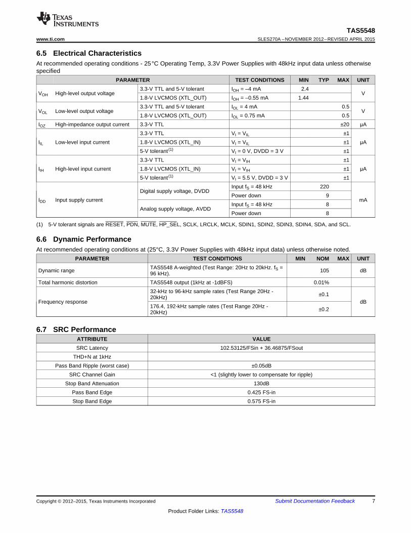
6.5 Electrical CharacteristicsAt recommended operating conditions - 25°C Operating Temp, 3.3V Power Supplies with 48kHz input data unless otherwisespecified
PARAMETER TEST CONDITIONS MIN TYP MAX UNIT3.3-V TTL and 5-V tolerant IOH = –4 mA 2.4
VOH High-level output voltage V1.8-V LVCMOS (XTL_OUT) IOH = –0.55 mA 1.443.3-V TTL and 5-V tolerant IOL = 4 mA 0.5
VOL Low-level output voltage V1.8-V LVCMOS (XTL_OUT) IOL = 0.75 mA 0.5
IOZ High-impedance output current 3.3-V TTL ±20 μA3.3-V TTL VI = VIL ±1
IIL Low-level input current 1.8-V LVCMOS (XTL_IN) VI = VIL ±1 μA5-V tolerant (1) VI = 0 V, DVDD = 3 V ±13.3-V TTL VI = VIH ±1
IIH High-level input current 1.8-V LVCMOS (XTL_IN) VI = VIH ±1 μA5-V tolerant (1) VI = 5.5 V, DVDD = 3 V ±1
Input fS = 48 kHz 220Digital supply voltage, DVDD
Power down 9IDD Input supply current mA
Input fS = 48 kHz 8Analog supply voltage, AVDD
Power down 8
(1) 5-V tolerant signals are RESET, PDN, MUTE, HP_SEL, SCLK, LRCLK, MCLK, SDIN1, SDIN2, SDIN3, SDIN4, SDA, and SCL.
6.6 Dynamic PerformanceAt recommended operating conditions at (25°C, 3.3V Power Supplies with 48kHz input data) unless otherwise noted.
PARAMETER TEST CONDITIONS MIN NOM MAX UNITTAS5548 A-weighted (Test Range: 20Hz to 20kHz. fS =Dynamic range 105 dB96 kHz).
Total harmonic distortion TAS5548 output (1kHz at -1dBFS) 0.01%32-kHz to 96-kHz sample rates (Test Range 20Hz - ±0.120kHz)
Frequency response dB176.4, 192-kHz sample rates (Test Range 20Hz - ±0.220kHz)
6.7 SRC PerformanceATTRIBUTE VALUESRC Latency 102.53125/FSin + 36.46875/FSout
THD+N at 1kHzPass Band Ripple (worst case) ±0.05dB
SRC Channel Gain <1 (slightly lower to compensate for ripple)Stop Band Attenuation 130dB
Pass Band Edge 0.425 FS-inStop Band Edge 0.575 FS-in
Copyright © 2012–2015, Texas Instruments Incorporated Submit Documentation Feedback 7
Product Folder Links: TAS5548
TAS5548SLES270A –NOVEMBER 2012–REVISED APRIL 2015 www.ti.com
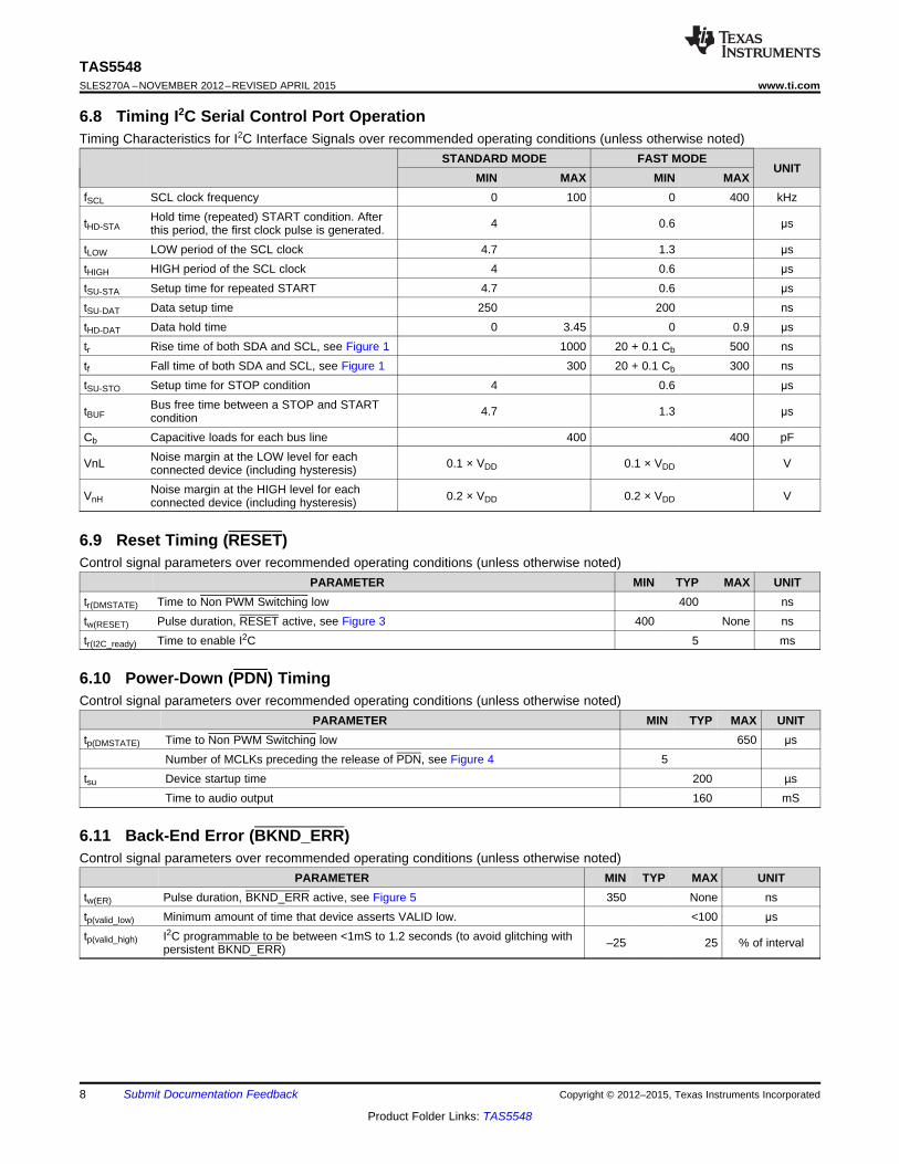
6.8 Timing I2C Serial Control Port OperationTiming Characteristics for I2C Interface Signals over recommended operating conditions (unless otherwise noted)
STANDARD MODE FAST MODEUNIT
MIN MAX MIN MAXfSCL SCL clock frequency 0 100 0 400 kHz
Hold time (repeated) START condition. AftertHD-STA 4 0.6 μsthis period, the first clock pulse is generated.tLOW LOW period of the SCL clock 4.7 1.3 μstHIGH HIGH period of the SCL clock 4 0.6 μstSU-STA Setup time for repeated START 4.7 0.6 μstSU-DAT Data setup time 250 200 nstHD-DAT Data hold time 0 3.45 0 0.9 μstr Rise time of both SDA and SCL, see Figure 1 1000 20 + 0.1 Cb 500 nstf Fall time of both SDA and SCL, see Figure 1 300 20 + 0.1 Cb 300 nstSU-STO Setup time for STOP condition 4 0.6 μs
Bus free time between a STOP and STARTtBUF 4.7 1.3 μsconditionCb Capacitive loads for each bus line 400 400 pF
Noise margin at the LOW level for eachVnL 0.1 × VDD 0.1 × VDD Vconnected device (including hysteresis)Noise margin at the HIGH level for eachVnH 0.2 × VDD 0.2 × VDD Vconnected device (including hysteresis)
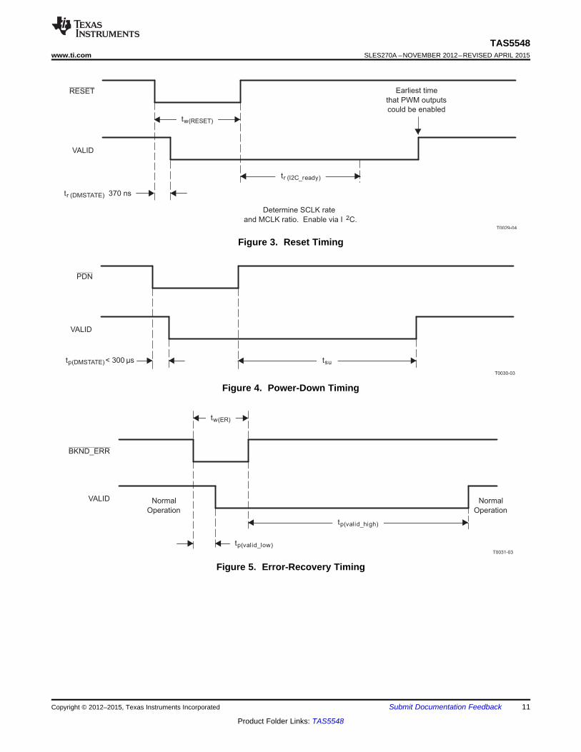
6.9 Reset Timing (RESET)Control signal parameters over recommended operating conditions (unless otherwise noted)
PARAMETER MIN TYP MAX UNITtr(DMSTATE) Time to Non PWM Switching low 400 nstw(RESET) Pulse duration, RESET active, see Figure 3 400 None nstr(I2C_ready) Time to enable I2C 5 ms
6.10 Power-Down (PDN) TimingControl signal parameters over recommended operating conditions (unless otherwise noted)
PARAMETER MIN TYP MAX UNITtp(DMSTATE) Time to Non PWM Switching low 650 μs
Number of MCLKs preceding the release of PDN, see Figure 4 5tsu Device startup time 200 µs
Time to audio output 160 mS
6.11 Back-End Error (BKND_ERR)Control signal parameters over recommended operating conditions (unless otherwise noted)
PARAMETER MIN TYP MAX UNITtw(ER) Pulse duration, BKND_ERR active, see Figure 5 350 None nstp(valid_low) Minimum amount of time that device asserts VALID low. <100 μstp(valid_high) I2C programmable to be between <1mS to 1.2 seconds (to avoid glitching with –25 25 % of intervalpersistent BKND_ERR)
8 Submit Documentation Feedback Copyright © 2012–2015, Texas Instruments Incorporated
Product Folder Links: TAS5548
TAS5548www.ti.com SLES270A –NOVEMBER 2012–REVISED APRIL 2015
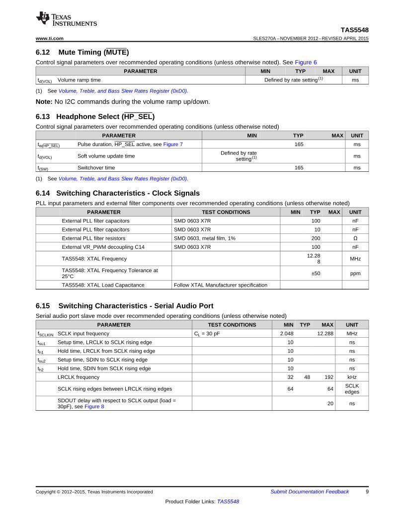
6.12 Mute Timing (MUTE)Control signal parameters over recommended operating conditions (unless otherwise noted). See Figure 6
PARAMETER MIN TYP MAX UNITtd(VOL) Volume ramp time Defined by rate setting (1) ms
(1) See Volume, Treble, and Bass Slew Rates Register (0xD0).
Note: No I2C commands during the volume ramp up/down.
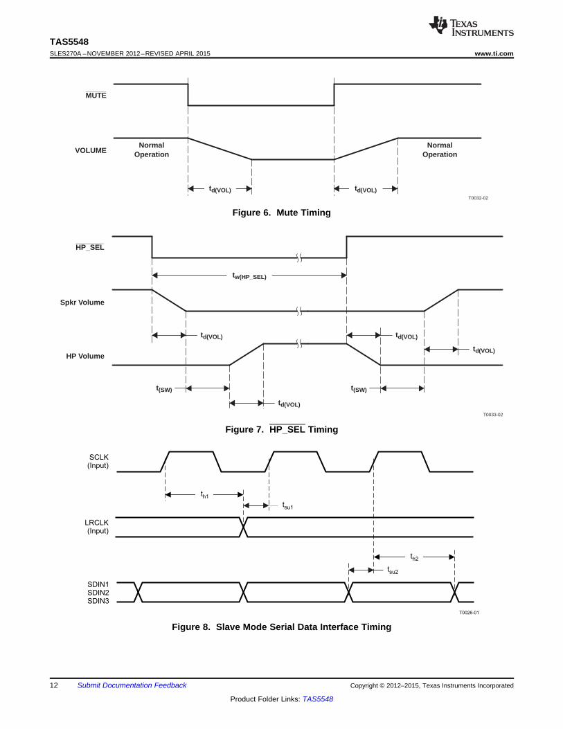
6.13 Headphone Select (HP_SEL)Control signal parameters over recommended operating conditions (unless otherwise noted)
PARAMETER MIN TYP MAX UNITtw(HP_SEL) Pulse duration, HP_SEL active, see Figure 7 165 ms
Defined by ratetd(VOL) Soft volume update time mssetting (1)
t(SW) Switchover time 165 ms
(1) See Volume, Treble, and Bass Slew Rates Register (0xD0).
6.14 Switching Characteristics - Clock SignalsPLL input parameters and external filter components over recommended operating conditions (unless otherwise noted)
PARAMETER TEST CONDITIONS MIN TYP MAX UNITExternal PLL filter capacitors SMD 0603 X7R 100 nFExternal PLL filter capacitors SMD 0603 X7R 10 nFExternal PLL filter resistors SMD 0603, metal film, 1% 200 ΩExternal VR_PWM decoupling C14 SMD 0603 X7R 100 nF
12.28TAS5548: XTAL Frequency MHz8TAS5548: XTAL Frequency Tolerance at ±50 ppm25°CTAS5548: XTAL Load Capacitance Follow XTAL Manufacturer specification
6.15 Switching Characteristics - Serial Audio PortSerial audio port slave mode over recommended operating conditions (unless otherwise noted)
PARAMETER TEST CONDITIONS MIN TYP MAX UNITfSCLKIN SCLK input frequency CL = 30 pF 2.048 12.288 MHztsu1 Setup time, LRCLK to SCLK rising edge 10 nsth1 Hold time, LRCLK from SCLK rising edge 10 nstsu2 Setup time, SDIN to SCLK rising edge 10 nsth2 Hold time, SDIN from SCLK rising edge 10 ns
LRCLK frequency 32 48 192 kHzSCLKSCLK rising edges between LRCLK rising edges 64 64 edges
SDOUT delay with respect to SCLK output (load = 20 ns30pF), see Figure 8
Copyright © 2012–2015, Texas Instruments Incorporated Submit Documentation Feedback 9
Product Folder Links: TAS5548
t(buf)
SCL
SDA
START Condition STOP Condition
th2
tsu3tsu2
TAS5548SLES270A –NOVEMBER 2012–REVISED APRIL 2015 www.ti.com
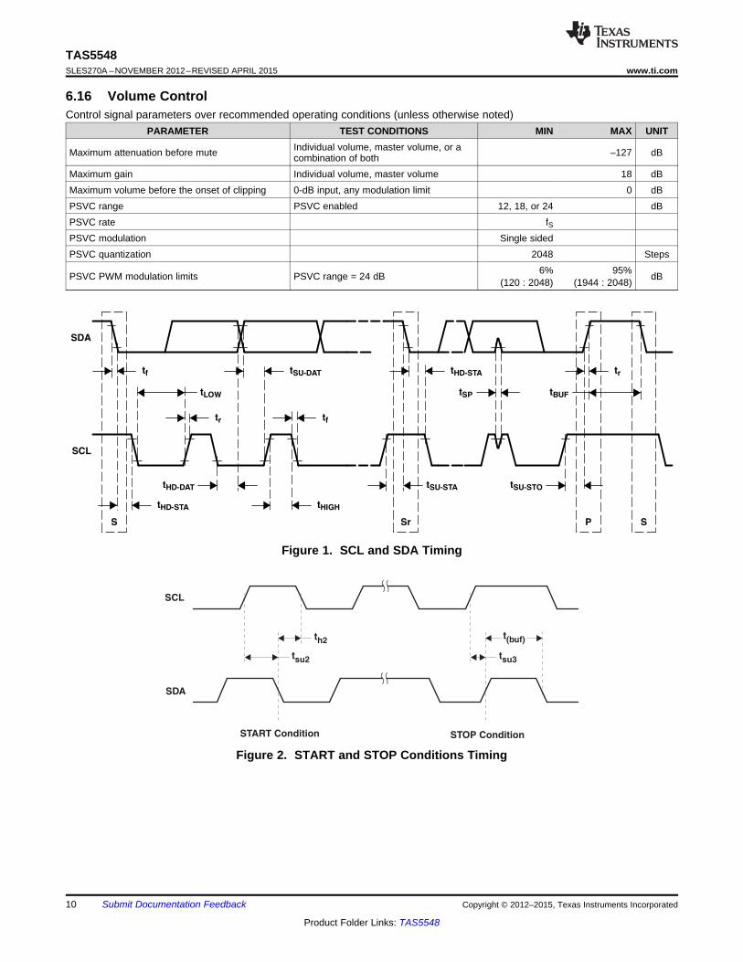
6.16 Volume ControlControl signal parameters over recommended operating conditions (unless otherwise noted)
PARAMETER TEST CONDITIONS MIN MAX UNITIndividual volume, master volume, or aMaximum attenuation before mute –127 dBcombination of both
Maximum gain Individual volume, master volume 18 dBMaximum volume before the onset of clipping 0-dB input, any modulation limit 0 dBPSVC range PSVC enabled 12, 18, or 24 dBPSVC rate fSPSVC modulation Single sidedPSVC quantization 2048 Steps
6% 95%PSVC PWM modulation limits PSVC range = 24 dB dB(120 : 2048) (1944 : 2048)
Figure 1. SCL and SDA Timing
Figure 2. START and STOP Conditions Timing
10 Submit Documentation Feedback Copyright © 2012–2015, Texas Instruments Incorporated
Product Folder Links: TAS5548
BKND_ERR
tp(valid_low)
VALID
tw(ER)
tp(valid_high)
Normal
Operation
Normal
Operation
T0031-03
PDN
VALID
tsutp(DMSTATE)< 300 µs
T0030-03
tw(RESET)
Earliest time
that PWM outputs
could be enabled
RESET
VALID
tr (DMSTATE) 370 ns
tr (I2C_ready)
Determine SCLK rate
and MCLK ratio. Enable via I 2C.T0029-04
TAS5548www.ti.com SLES270A –NOVEMBER 2012–REVISED APRIL 2015
Figure 3. Reset Timing
Figure 4. Power-Down Timing
Figure 5. Error-Recovery Timing
Copyright © 2012–2015, Texas Instruments Incorporated Submit Documentation Feedback 11
Product Folder Links: TAS5548
th1
tsu1
tsu2
th2
SCLK(Input)
LRCLK(Input)
SDIN1SDIN2SDIN3
T0026-01
td(VOL)
HP Volume
HP_SEL
Spkr Volume
t(SW)
T0033-02
td(VOL)
td(VOL)
td(VOL)
t(SW)
tw(HP_SEL)
td(VOL)
VOLUME
MUTE
NormalOperation
NormalOperation
td(VOL)T0032-02
TAS5548SLES270A –NOVEMBER 2012–REVISED APRIL 2015 www.ti.com
Figure 6. Mute Timing
Figure 7. HP_SEL Timing
Figure 8. Slave Mode Serial Data Interface Timing
12 Submit Documentation Feedback Copyright © 2012–2015, Texas Instruments Incorporated
Product Folder Links: TAS5548
Frequency (Hz)
Am
plitu
de (
dB)
0 5000 10000 15000 20000-180
-160
-140
-120
-100
-80
-60
-40
-20
0
D003Frequency (Hz)
Am
plitu
de (
dB)
0 5000 10000 15000 20000 25000-200
-180
-160
-140
-120
-100
-80
-60
-40
-20
0
D004
Frequency (Hz)
Am
plitu
de (
dB)
0 5000 10000 15000 20000-180
-160
-140
-120
-100
-80
-60
-40
-20
0
D001Frequency (Hz)
Am
plitu
de (
dB)
0 5000 10000 15000 20000-180
-160
-140
-120
-100
-80
-60
-40
-20
0
D002
TAS5548www.ti.com SLES270A –NOVEMBER 2012–REVISED APRIL 2015
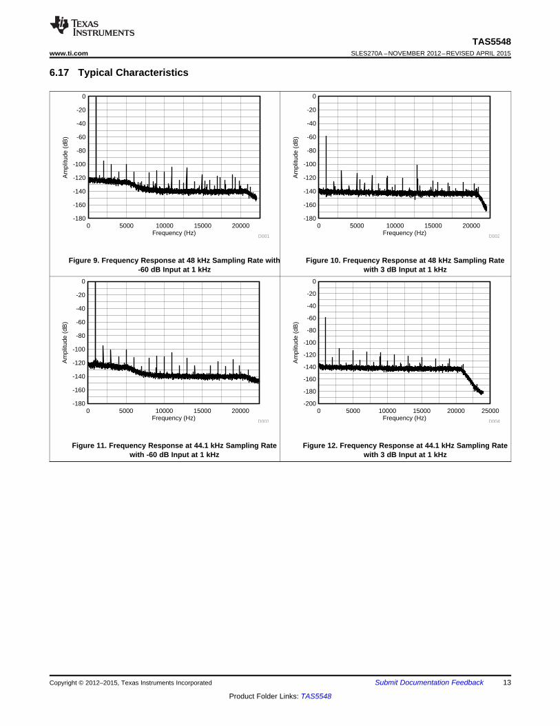
6.17 Typical Characteristics
Figure 9. Frequency Response at 48 kHz Sampling Rate with Figure 10. Frequency Response at 48 kHz Sampling Rate-60 dB Input at 1 kHz with 3 dB Input at 1 kHz
Figure 11. Frequency Response at 44.1 kHz Sampling Rate Figure 12. Frequency Response at 44.1 kHz Sampling Ratewith -60 dB Input at 1 kHz with 3 dB Input at 1 kHz
Copyright © 2012–2015, Texas Instruments Incorporated Submit Documentation Feedback 13
Product Folder Links: TAS5548
Serial Audio Receiver2x Stereo
Serial Audio Receiver2x Stereo
Serial Audio Transciever
Stereo
4ch ASRC
4ch ASRC
Fixed FlowDigital Audio Processor
(DAP)
10ch input8ch Processor
8ch Output Mixer
Clocks(Osc, PLL
etc)12.288
8ch PWM Generator+ Headphone
(PWM)Bypass
MCUI2C
Control
Power Supply Volume Control(PSVC)
Energy Manager (EMO)
Power
SD
A
SC
L
SDOUT/SDIN5
SDIN1
SDIN2
SCLK
LRCLK
SDIN2-1
SDIN2-2
SCLKO /SCLKIN_2
LRCLKO / LRCKIN_2
OS
CR
ES
PLL
_FLT
M
PLL
_FLT
P
MC
LK
EM
O1
AS
EL_
EM
O2
PS
VC
/MC
LKO
VR
_DIG
VR
_PW
M
VR
_AN
A
AV
DD
AVDD_PWM
AVSS
AVSS_PWM
DVDD1
DVDD2
DVSS1
DVSS2
/PDN
PWM_HPM_L&R
PWM_HPP_L&R
/BKND_ERR
PWM_x_1 through 8
AS
EL_
EM
O2
VALID
/MUTE
TE
ST
RE
SE
T
/HP
_SE
L
TAS5548SLES270A –NOVEMBER 2012–REVISED APRIL 2015 www.ti.com
7 Detailed Description
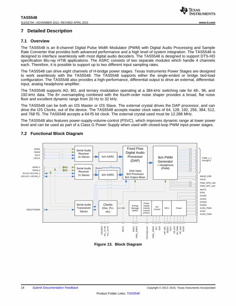
7.1 OverviewThe TAS5548 is an 8-channel Digital Pulse Width Modulator (PWM) with Digital Audio Processing and SampleRate Converter that provides both advanced performance and a high level of system integration. The TAS5548 isdesigned to interface seamlessly with most digital audio decoders. The TAS5548 is designed to support DTS-HDspecification Blu-ray HTiB applications. The ASRC consists of two separate modules which handle 4 channelseach. Therefore, it is possible to support up to two different input sampling rates.
The TAS5548 can drive eight channels of H-bridge power stages. Texas Instruments Power Stages are designedto work seamlessly with the TAS5548. The TAS5548 supports either the single-ended or bridge tied-loadconfiguration. The TAS5548 also provides a high-performance, differential output to drive an external, differential-input, analog headphone amplifier.
The TAS5548 supports AD, BD, and ternary modulation operating at a 384-kHz switching rate for 48-, 96, and192-kHz data. The 8× oversampling combined with the fourth-order noise shaper provides a broad, flat noisefloor and excellent dynamic range from 20 Hz to 32 kHz.
The TAS5548 can be both an I2S Master or I2S Slave. The external crystal drives the DAP processor, and candrive the I2S Clocks, out of the device. The TAS5548 accepts master clock rates of 64, 128, 192, 256, 384, 512,and 768 fS. The TAS5548 accepts a 64-fS bit clock. The external crystal used must be 12.288 MHz.
The TAS5548 also features power-supply-volume-control (PSVC), which improves dynamic range at lower powerlevel and can be used as part of a Class G Power Supply when used with closed-loop PWM input power stages.
7.2 Functional Block Diagram
Figure 13. Block Diagram
14 Submit Documentation Feedback Copyright © 2012–2015, Texas Instruments Incorporated
Product Folder Links: TAS5548
Digital Audio Processor Core
IN1
COEF
RAM
Data
RAM
Code
ROMController
8052
MCU
(8-Bit)
8
ExternalDataRAM
InternalDataRAM
CodeROM
SCL
SDA
CS0
8
8
54
32
28
32
32
32
32
IN2
IN4
IN3
MemoryInterface
T/B
Control
RegistersI2C
Serial
Interface
Data
Path
Micro Core
TO
PWM
IN5
OUT 2
IN7
IN6
IN8
IN9
IN10
OUT 1
24
24
24
24
24
24
24
24
24
24
24
24
TAS5548www.ti.com SLES270A –NOVEMBER 2012–REVISED APRIL 2015
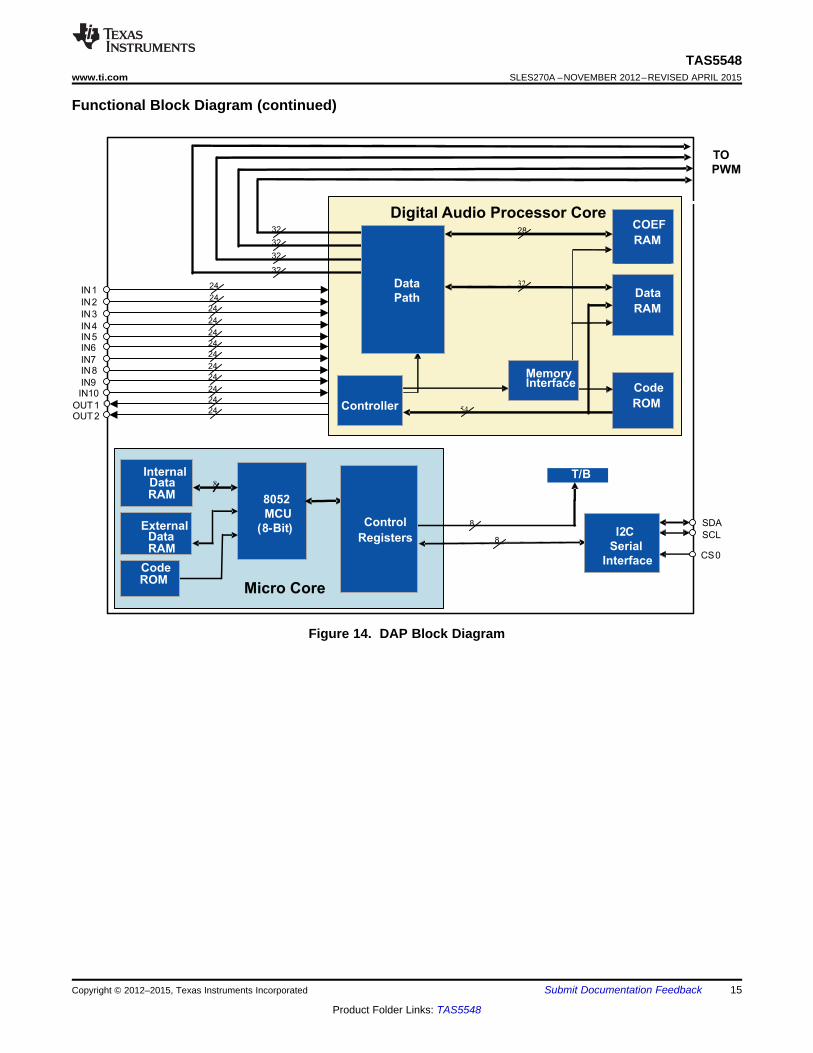
Functional Block Diagram (continued)
Figure 14. DAP Block Diagram
Copyright © 2012–2015, Texas Instruments Incorporated Submit Documentation Feedback 15
Product Folder Links: TAS5548
23 22
SCLK
32 Clks
LRCLK (Note Reversed Phase) Left Channel
24-Bit Mode
1
19 18
20-Bit Mode
16-Bit Mode
15 14
MSB LSB
32 Clks
Right Channel
2-Channel I S (Philips Format) Stereo Input2
T0034-01
5 49 8
1 0
0
45
1 0
23 22 1
19 18
15 14
MSB LSB
5 49 8
1 0
0
45
1 0
SCLK
TAS5548SLES270A –NOVEMBER 2012–REVISED APRIL 2015 www.ti.com
7.3 Feature Description
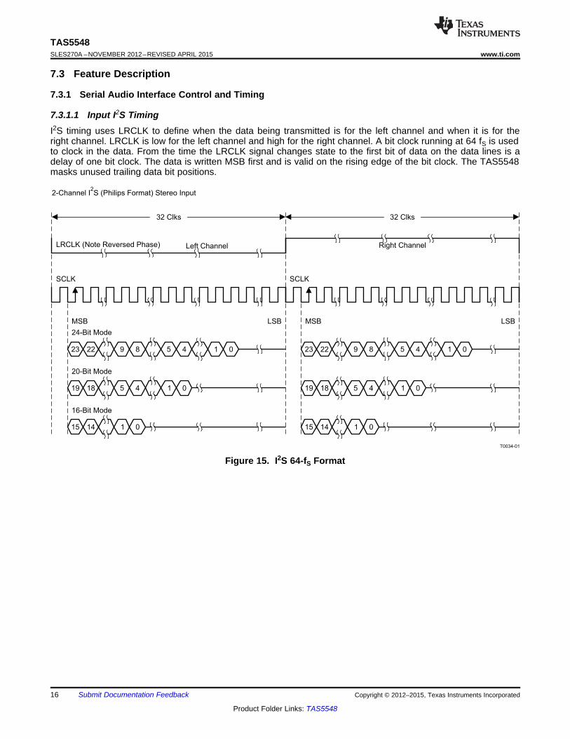
7.3.1 Serial Audio Interface Control and Timing
7.3.1.1 Input I2S TimingI2S timing uses LRCLK to define when the data being transmitted is for the left channel and when it is for theright channel. LRCLK is low for the left channel and high for the right channel. A bit clock running at 64 fS is usedto clock in the data. From the time the LRCLK signal changes state to the first bit of data on the data lines is adelay of one bit clock. The data is written MSB first and is valid on the rising edge of the bit clock. The TAS5548masks unused trailing data bit positions.
Figure 15. I2S 64-fS Format
16 Submit Documentation Feedback Copyright © 2012–2015, Texas Instruments Incorporated
Product Folder Links: TAS5548
23 22
SCLK
32 Clks
LRCLK
Left Channel
24-Bit Mode
1
19 18
20-Bit Mode
16-Bit Mode
15 14
MSB LSB
32 Clks
Right Channel
2-Channel Left-Justified Stereo Input
T0034-02
459 8
145
1
0
0
0
23 22 1
19 18
15 14
MSB LSB
459 8
145
1
0
0
0
SCLK
TAS5548www.ti.com SLES270A –NOVEMBER 2012–REVISED APRIL 2015
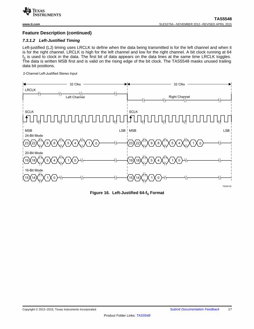
Feature Description (continued)7.3.1.2 Left-Justified TimingLeft-justified (LJ) timing uses LRCLK to define when the data being transmitted is for the left channel and when itis for the right channel. LRCLK is high for the left channel and low for the right channel. A bit clock running at 64fS is used to clock in the data. The first bit of data appears on the data lines at the same time LRCLK toggles.The data is written MSB first and is valid on the rising edge of the bit clock. The TAS5548 masks unused trailingdata bit positions.
Figure 16. Left-Justified 64-fS Format
Copyright © 2012–2015, Texas Instruments Incorporated Submit Documentation Feedback 17
Product Folder Links: TAS5548
23 22
SCLK
32 Clks
LRCLK
Left Channel
24-Bit Mode
1
20-Bit Mode
16-Bit Mode
15 14
MSB LSB
SCLK
32 Clks
Right Channel
2-Channel Right-Justified (Sony Format) Stereo Input
T0034-03
19 18
119 18
1
0
0
0
15 14
15 14 23 22 1
15 14
MSB LSB
19 18
119 18
1
0
0
0
15 14
15 14
TAS5548SLES270A –NOVEMBER 2012–REVISED APRIL 2015 www.ti.com
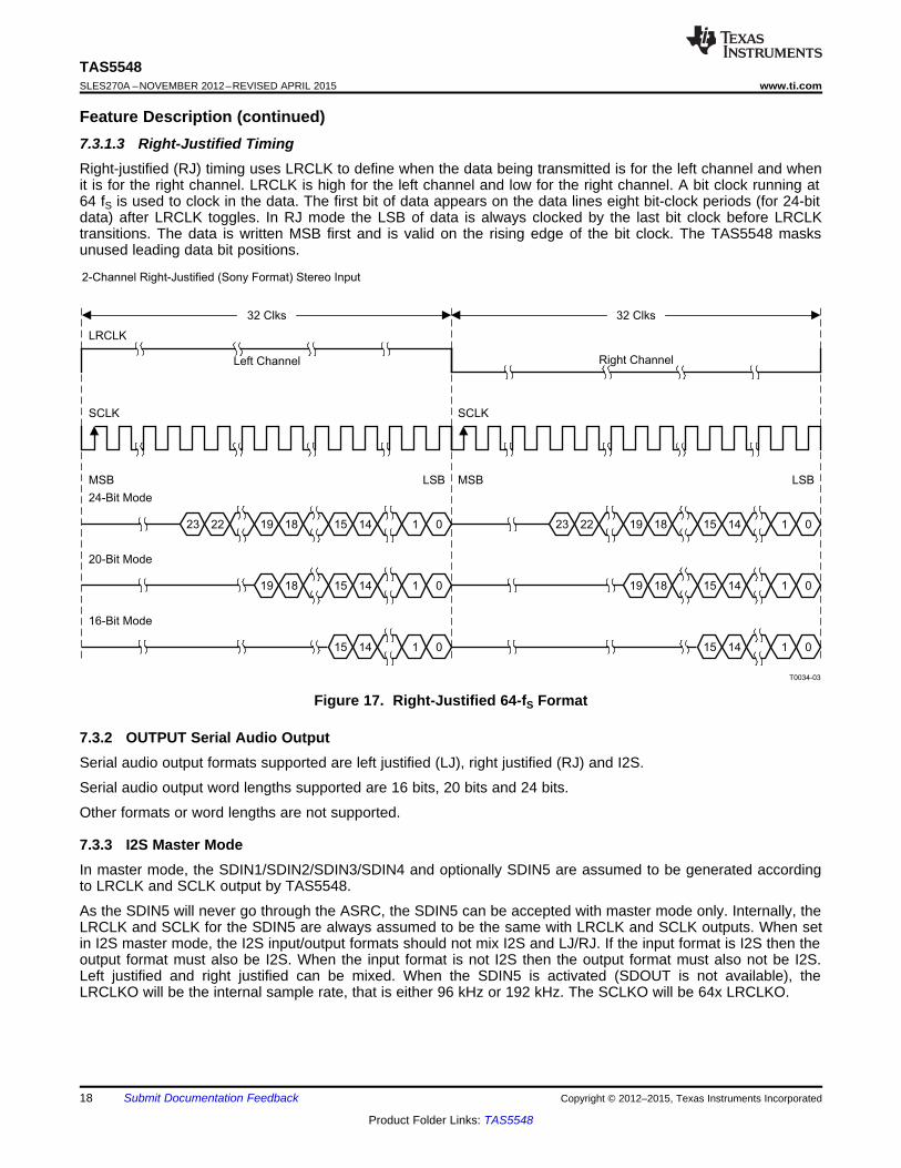
Feature Description (continued)7.3.1.3 Right-Justified TimingRight-justified (RJ) timing uses LRCLK to define when the data being transmitted is for the left channel and whenit is for the right channel. LRCLK is high for the left channel and low for the right channel. A bit clock running at64 fS is used to clock in the data. The first bit of data appears on the data lines eight bit-clock periods (for 24-bitdata) after LRCLK toggles. In RJ mode the LSB of data is always clocked by the last bit clock before LRCLKtransitions. The data is written MSB first and is valid on the rising edge of the bit clock. The TAS5548 masksunused leading data bit positions.
Figure 17. Right-Justified 64-fS Format
7.3.2 OUTPUT Serial Audio OutputSerial audio output formats supported are left justified (LJ), right justified (RJ) and I2S.
Serial audio output word lengths supported are 16 bits, 20 bits and 24 bits.
Other formats or word lengths are not supported.
7.3.3 I2S Master ModeIn master mode, the SDIN1/SDIN2/SDIN3/SDIN4 and optionally SDIN5 are assumed to be generated accordingto LRCLK and SCLK output by TAS5548.
As the SDIN5 will never go through the ASRC, the SDIN5 can be accepted with master mode only. Internally, theLRCLK and SCLK for the SDIN5 are always assumed to be the same with LRCLK and SCLK outputs. When setin I2S master mode, the I2S input/output formats should not mix I2S and LJ/RJ. If the input format is I2S then theoutput format must also be I2S. When the input format is not I2S then the output format must also not be I2S.Left justified and right justified can be mixed. When the SDIN5 is activated (SDOUT is not available), theLRCLKO will be the internal sample rate, that is either 96 kHz or 192 kHz. The SCLKO will be 64x LRCLKO.
18 Submit Documentation Feedback Copyright © 2012–2015, Texas Instruments Incorporated
Product Folder Links: TAS5548
TAS5548www.ti.com SLES270A –NOVEMBER 2012–REVISED APRIL 2015
Feature Description (continued)7.3.4 LRCKO and SCLKOThere are output pins for LRCLK output and SCK output. As the SDIN5 rate (which always follow internal samplerate) and the SDOUT rate (which is 44.1 kHz or 48 kHz) is different, the LRCLKO will be the internal sample rate(96 kHz or 192 kHz) when SDIN5 is activated (SDOUT is not available) and it will be 44.1 kHz or 48 kHz whenSDOUT is available. The SCLKO will be always 64x LRCLKO.
8.5 Master Clock Output (MCLKO) Master clock is generated from the MCLK input itself. There is a clock dividerwith division factor of 4, 2 or 1 that can be selected from. The default is no division
7.3.5 PWM FeaturesThe TAS5548 has eight channels of high-performance digital PWM modulators that are designed to driveswitching output stages (back ends) in both single-ended (SE) and bridge-tied-load (BTL) configurations. Thedevice uses noise-shaping and sophisticated, error-correction algorithms to achieve high power efficiency andhigh-performance digital audio reproduction. The TAS5548 uses an AD/BD/Ternary PWM modulation schemecombined with a fourth-order noise shaper to provide a >105-dB SNR from 20 Hz to 20 kHz.
The PWM section accepts 32-bit PCM data from the DAP and outputs eight PWM audio output channelsconfigurable as either:• Six channels to drive power stages and two channels to drive a differential-input active filter to provide a
separately controllable stereo lineout• Eight channels to drive power stages
The PWM section provides a headphone PWM output to drive an external differential amplifier like theTPA6139A2. The headphone circuit uses the PWM modulator for channels 1 and 2. The headphone does notoperate while the six or eight back-end drive channels are operating. The headphone is enabled via aheadphone-select terminal.
The PWM section also contains the power-supply volume control (PSVC) PWM.
The interpolator, noise shaper, and PWM sections provide a PWM output with the following features:• Up to 8× oversampling
– 4× at fS = 88.2 kHz, 96 kHz– 2× at fS = 176.4 kHz, 192 kHz
• Fourth-order noise shaping• 105-dB dynamic range 0–20 kHz (TAS5548 + TAS5614 system measured at speaker terminals)• THD < 0.01%• Adjustable modulation limit of 87.4% to 99.2%• 3.3-V digital signal
7.3.5.1 DC Blocking (High-Pass Filter Enable/Disable)Each input channel incorporates a first-order, digital, high-pass filter to block potential dc components. The filter–3-dB point is approximately 2-Hz at the 96-kHz sampling rate. The high-pass filter can be enabled and disabledvia the I2C system control register 1 (0x03 bit D7). The default setting is 1 (high-pass filter enabled).
7.3.5.2 AM Interference AvoidanceDigital amplifiers can degrade AM reception as a result of their RF emissions. Texas Instruments' patented AMinterference-avoidance circuit provides a flexible system solution for a wide variety of digital audio architectures.During AM reception, the TAS5548 adjusts the radiated emissions to provide an emission-clear zone for thetuned AM frequency. The inputs to the TAS5548 for this operation are the tuned AM frequency, the IF frequency,and the sample rate. This PWM rate modification is done by modifying the output rate of the Sample RateConverter, and the following DSP and PWM modulator.
7.3.6 TAS5548 Controls and StatusThe TAS5548 provides control and status information from both the I2C registers and device pins.
Copyright © 2012–2015, Texas Instruments Incorporated Submit Documentation Feedback 19
Product Folder Links: TAS5548
TAS5548SLES270A –NOVEMBER 2012–REVISED APRIL 2015 www.ti.com
Feature Description (continued)This section describes some of these controls and status functions. The I2C summary and detailed registerdescriptions are contained in Register Maps and I 2C Serial-Control Interface.
7.3.6.1 I2C Status RegistersThe TAS5548 has two status registers that provide general device information. These are the general statusregister 0 (0x01) and the error status register (0x02).
7.3.6.1.1 General Status Register (0x01)• Device identification code
7.3.6.1.2 Error Status Register (0x02)• No internal errors (the valid signal is high)• Audio Clip indicator. Writing to the register clears the indicator.• This error status register is normally used for system development only.
7.3.6.2 TAS5548 Pin ControlsThe TAS5548 provide a number of terminal controls to manage the device operation. These controls are:• RESET• PDN• BKND_ERR• HP_SEL• MUTE• PSVC• EMO1 (see System Power Contoller section)• EMO2 (see System Power Contoller section)
7.3.6.2.1 Reset (RESET)
The TAS5548 is placed in the reset mode either by the power-up reset circuitry when power is applied, or bysetting the RESET terminal low.
RESET is an asynchronous control signal that restores the TAS5548 to the hard-mute state (Non PWMSwitching). Master volume is immediately set to full attenuation (there is no ramp down). Reset initiates thedevice reset without an MCLK input. As long as the RESET terminal is held low, the device is in the reset state.During reset, all I2C and serial data bus operations are ignored.
Table 1 shows the device output signals while RESET is active.
Table 1. Device Outputs During ResetSIGNAL SIGNAL STATE
Valid LowPWM P-outputs Low (Non PWM Switching)PWM M-outputs Low (Non PWM Switching)
SDA Signal input (not driven)
Because RESET is an asynchronous signal, clicks and pops produced during the application (the leading edge)of RESET cannot be avoided. However, the transition from the hard-mute state (Non PWM Switching) to theoperational state is performed using a quiet start-up sequence to minimize noise. This control uses the PWMreset and unmute sequence to shut down and start up the PWM. If a completely quiet reset or power-downsequence is desired, MUTE should be applied before applying RESET.
The rising edge of the reset pulse begins device initialization before the transition to the operational mode.During device initialization, all controls are reset to their initial states. Table 2 shows the default control settingsfollowing a reset.
20 Submit Documentation Feedback Copyright © 2012–2015, Texas Instruments Incorporated
Product Folder Links: TAS5548
TAS5548www.ti.com SLES270A –NOVEMBER 2012–REVISED APRIL 2015
Table 2. Values Set During ResetCONTROL SETTING
Output mixer configuration 0xD0 bit 30 = 0 (remapped output mixer configuration)High pass EnabledUnmute from clock error Hard unmuteInput automute EnabledOutput automute EnabledSerial data interface format I2S, 24-bitIndividual channel mute No channels are mutedAutomute delay 14.9 msAutomute threshold 1 < 8 bitsAutomute threshold 2 Same as automute threshold 1Modulation limit 93.7% (Note: Some power stages require a lower
modulation index)Six- or eight-channel configuration Eight channelsVolume and mute update rate Volume ramp 42.6 msTreble and bass slew rate Update every 1.31 msBank switching Manual bank selection is enabledBiquad coefficients Set to all passInput mixer coefficients Input N → Channel N, no attenuationOutput mixer coefficients Channel N → Output N, no attenuationSubwoofer sum into Ch1 and Ch2 Gain of 0Ch1 and Ch2 sum in subwoofer Gain of 0Bass and treble bypass/inline BypassDRC bypass/inline BypassDRC Default valuesMaster volume MuteIndividual channel volumes 0 dBAll bass and treble indexes 0 dBTreble filter sets Filter set 3Bass filter sets Filter set 3Loudness Loudness disabled, default valuesAM interference mode enable DisabledAM interference mode IF 455 kHzAM interference mode select sequence 1AM interference mode tuned frequency and 0000, BCDinput mode
After the initialization time, the TAS5548 starts the transition to the operational state with the master volume setat mute.
Because the TAS5548 has an internal oscillator time base, following the release of reset, oscillator trimcommand is needed so the TAS5548 can detect the MCLK and data rate and perform the initializationsequences. The PWM outputs are held at a mute state until the master volume is set to a value other than mutevia I2C.
7.3.6.2.2 Power Down (PDN)
The TAS5548 can be placed into the power-down mode by holding the PDN terminal low. When the power-downmode is entered, both the PLL and the oscillator are shut down. Volume is immediately set to full attenuation(there is no ramp down). This control uses the PWM mute sequence that provides a low click and pop transitionto a non PWM switching mute state.
Copyright © 2012–2015, Texas Instruments Incorporated Submit Documentation Feedback 21
Product Folder Links: TAS5548
TAS5548SLES270A –NOVEMBER 2012–REVISED APRIL 2015 www.ti.com
Power down is an asynchronous operation that does not require MCLK to go into the power-down state. Toinitiate the power-up sequence requires MCLK to be operational and the TAS5548 to receive five MCLKs prior tothe release of PDN.
As long as the PDN pin is held low, the device is in the power-down state with the PWM outputs not switching.During power down, all I2C and serial data bus operations are ignored. Table 3 shows the device output signalswhile PDN is active.
Table 3. Device Outputs During Power DownSIGNAL SIGNAL STATEVALID Low
PWM P-outputs Not Switching = LowPWM M-outputs Not Switching = Low
SDA Inputs IgnoredPSVC Low
Following the application of PDN, the TAS5548 does not perform a quiet shutdown to prevent clicks and popsproduced during the application (the leading edge) of this command. The application of PDN immediatelyperforms a PWM stop. A quiet stop sequence can be performed by first applying MUTE before PDN.
When PDN is released, the system goes to the end state specified by the MUTE and BKND_ERR pins and theI2C register settings.
7.3.6.2.3 Back-End Error (BKND_ERR)
Back-end error is used to provide error management for back-end error conditions. Back-end error is a level-sensitive signal. Back-end error can be initiated by bringing the BKND_ERR terminal low for a minimum of fiveMCLK cycles. When BKND_ERR is brought low, the PWM sets either six or eight channels into the PWM back-end error state. This state is described in PWM Features. Once the back-end error is removed, a delay of 5 ms isperformed before the system starts the output re-initialization sequence. After the initialization time, the TAS5548begins normal operation. During back-end error I2C registers retain current values.
Table 4. Device Outputs During Back-End ErrorSIGNAL SIGNAL STATE
Valid LowPWM P-outputs Non PWM Switching = lowPWM M-outputs Non PWM Switching = low
PWM_HP P-outputs Non PWM Switching = lowPWM_HP M-outputs Non PWM Switching = low
SDA Signal input (not driven)
7.3.6.2.3.1 BKND_ERR and VALID
The number of channels that are affected by the BKND_ERR signal depends on the setting of bit D1 of I2Cregister 0xE0. If the I2C setting (of bit D1) is 0 (8-channel mode), the TAS5548 places all eight PWM outputs inthe PWM back-end error state. If the I2C setting (of bit D1) is 1, the TAS5548 is in 6-channel mode. For properoperation in 6-channel mode, the lineout configuration registers (0x09 and 0x0A) must be 0x00 instead of thedefault of 0xE0. In this case, VALID is pulled LOW, and the TAS5548 brings PWM outputs 1, 2, 3, 4, 7, and 8 toa back-end error state, while not affecting lineout channels 5 and 6. Table 4 shows the device output signalstates during back-end error.
7.3.6.2.4 Speaker/Headphone Selector (HP_SEL)
The HP_SEL terminal enables the headphone output or the speaker outputs. The headphone output receives theprocessed data output from DAP and PWM channels 1 and 2.
In 6-channel configuration, this feature does not affect the two lineout channels.
When low, the headphone output is enabled. In this mode, the speaker outputs are disabled. When high, thespeaker outputs are enabled and the headphone is disabled.
22 Submit Documentation Feedback Copyright © 2012–2015, Texas Instruments Incorporated
Product Folder Links: TAS5548
TAS5548www.ti.com SLES270A –NOVEMBER 2012–REVISED APRIL 2015
Changes in the pin logic level result in a state change sequence using soft mute (PWM switching at 50/50, noiseshaper on) to the hard mute (non-PWM switching) mode for both speaker and headphone followed by a softunmute.
When HP_SEL is low, the configuration of channels 1 and 2 is defined by the headphone configuration register.When HP_SEL is high, the channel-1 and -2 configuration registers define the configuration of channels 1 and 2.
If using the remapped-output mixer configuration (0xD0 bit 30 = 0) in the 6-channel mode, the headphoneoperation is modified. That is, following the assertion or de-assertion of headphone, mute must be asserted andde-asserted using the MUTE pin.
7.3.6.2.5 Mute (MUTE)
The mute control provides a noiseless volume ramp to silence. Releasing mute provides a noiseless ramp toprevious volume. The TAS5548 has both master and individual channel mute commands. A terminal is alsoprovided for the master mute. The master mute I2C register and the MUTE terminal are logically ORed together.If either is asserted, a mute on all channels is performed. The master mute command operates on all channelsregardless of whether the system is in the 6- or 8-channel configuration. PWM is switching at 50% duty cycleduring mute.
The master mute terminal is used to support a variety of other operations in the TAS5548, such as setting thebiquad coefficients, the serial interface format, and the clock rates. A mute command by the master muteterminal, individual I2C mute, the AM interference mute sequence, the bank-switch mute sequence, or automuteoverrides an unmute command or a volume command. While a mute is active, the commanded channels areplaced in a mute state. When a channel is unmuted, it goes to the last commanded volume setting that has beenreceived for that channel.
Copyright © 2012–2015, Texas Instruments Incorporated Submit Documentation Feedback 23
Product Folder Links: TAS5548
G003
Desired Gain − Linear
Pow
er-S
uppl
y an
d D
igita
l Gai
ns −
dB
Digital Gain
Power-Supply Gain
0.00001 0.1 1000.0001
0.01
10
100
1
0.001
0.1
1
100.0001 0.001 0.01
−60
−50
−40
−30
−20
−10
0
10
20
30
−80 −70 −60 −50 −40 −30 −20 −10 0 10 20 30
Desired Gain − dB
Pow
er-S
uppl
y an
d D
igita
l Gai
ns −
dB
Digital Gain
Power-Supply Gain
G002
TAS5548SLES270A –NOVEMBER 2012–REVISED APRIL 2015 www.ti.com
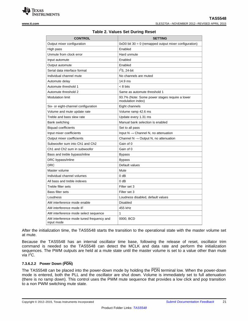
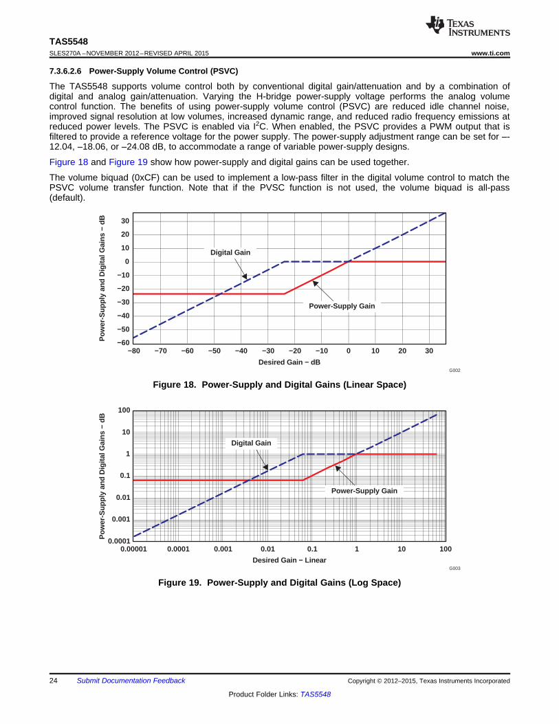
7.3.6.2.6 Power-Supply Volume Control (PSVC)
The TAS5548 supports volume control both by conventional digital gain/attenuation and by a combination ofdigital and analog gain/attenuation. Varying the H-bridge power-supply voltage performs the analog volumecontrol function. The benefits of using power-supply volume control (PSVC) are reduced idle channel noise,improved signal resolution at low volumes, increased dynamic range, and reduced radio frequency emissions atreduced power levels. The PSVC is enabled via I2C. When enabled, the PSVC provides a PWM output that isfiltered to provide a reference voltage for the power supply. The power-supply adjustment range can be set for –-12.04, –18.06, or –24.08 dB, to accommodate a range of variable power-supply designs.
Figure 18 and Figure 19 show how power-supply and digital gains can be used together.
The volume biquad (0xCF) can be used to implement a low-pass filter in the digital volume control to match thePSVC volume transfer function. Note that if the PVSC function is not used, the volume biquad is all-pass(default).
Figure 18. Power-Supply and Digital Gains (Linear Space)
Figure 19. Power-Supply and Digital Gains (Log Space)
24 Submit Documentation Feedback Copyright © 2012–2015, Texas Instruments Incorporated
Product Folder Links: TAS5548
TAS5548www.ti.com SLES270A –NOVEMBER 2012–REVISED APRIL 2015
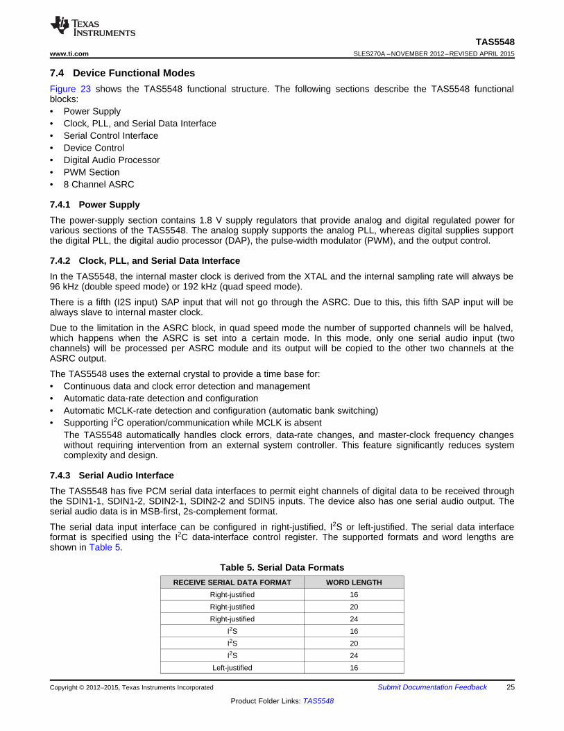
7.4 Device Functional ModesFigure 23 shows the TAS5548 functional structure. The following sections describe the TAS5548 functionalblocks:• Power Supply• Clock, PLL, and Serial Data Interface• Serial Control Interface• Device Control• Digital Audio Processor• PWM Section• 8 Channel ASRC
7.4.1 Power SupplyThe power-supply section contains 1.8 V supply regulators that provide analog and digital regulated power forvarious sections of the TAS5548. The analog supply supports the analog PLL, whereas digital supplies supportthe digital PLL, the digital audio processor (DAP), the pulse-width modulator (PWM), and the output control.
7.4.2 Clock, PLL, and Serial Data InterfaceIn the TAS5548, the internal master clock is derived from the XTAL and the internal sampling rate will always be96 kHz (double speed mode) or 192 kHz (quad speed mode).
There is a fifth (I2S input) SAP input that will not go through the ASRC. Due to this, this fifth SAP input will bealways slave to internal master clock.
Due to the limitation in the ASRC block, in quad speed mode the number of supported channels will be halved,which happens when the ASRC is set into a certain mode. In this mode, only one serial audio input (twochannels) will be processed per ASRC module and its output will be copied to the other two channels at theASRC output.
The TAS5548 uses the external crystal to provide a time base for:• Continuous data and clock error detection and management• Automatic data-rate detection and configuration• Automatic MCLK-rate detection and configuration (automatic bank switching)• Supporting I2C operation/communication while MCLK is absent
The TAS5548 automatically handles clock errors, data-rate changes, and master-clock frequency changeswithout requiring intervention from an external system controller. This feature significantly reduces systemcomplexity and design.
7.4.3 Serial Audio InterfaceThe TAS5548 has five PCM serial data interfaces to permit eight channels of digital data to be received throughthe SDIN1-1, SDIN1-2, SDIN2-1, SDIN2-2 and SDIN5 inputs. The device also has one serial audio output. Theserial audio data is in MSB-first, 2s-complement format.
The serial data input interface can be configured in right-justified, I2S or left-justified. The serial data interfaceformat is specified using the I2C data-interface control register. The supported formats and word lengths areshown in Table 5.
Table 5. Serial Data FormatsRECEIVE SERIAL DATA FORMAT WORD LENGTH
Right-justified 16Right-justified 20Right-justified 24
I2S 16I2S 20I2S 24
Left-justified 16
Copyright © 2012–2015, Texas Instruments Incorporated Submit Documentation Feedback 25
Product Folder Links: TAS5548
TAS5548SLES270A –NOVEMBER 2012–REVISED APRIL 2015 www.ti.com
Table 5. Serial Data Formats (continued)RECEIVE SERIAL DATA FORMAT WORD LENGTH
Left-justified 20Left-justified 24
Serial data is input on SDIN1-SDIN5. The device will accept 32, 44.1, 48, 88.2, 96, 176.4 and 192 kHz serialdata in 16, 20 or 24-bit data in Left, Right and I2S serial data formats using a 64 Fs SCLK clock and a 64, 128,192, 256, 384, or 512 * Fs MCLK rates (up to a maximum of 50 MHz).
NOTETo run MCLK at 64 Fs, the source signal must be at least 48 kHz.
Serial Data is output on SDOUT. The SDOUT data format is I2S 24 bit.
The parameters of this clock and serial data interface are I2C configurable. But the default is autodetect.
7.4.4 I 2C Serial-Control InterfaceThe TAS5548 has an I2C serial-control slave interface to receive commands from a system controller. The serial-control interface supports both normal-speed (100-kHz) and high-speed (400-kHz) operations without wait states.
The serial control interface supports both single-byte and multiple-byte read/write operations for status registersand the general control registers associated with the PWM. However, for the DAP data-processing registers, theserial control interface also supports multiple-byte (4-byte) write operations.
The I2C supports a special mode which permits I2C write operations to be broken up into multiple data-writeoperations that are multiples of 4 data bytes. These are 6-byte, 10-byte, 14-byte, 18-byte, etc., write operationsthat are composed of a device address, read/write bit, subaddress, and any multiple of 4 bytes of data. Thispermits the system to incrementally write large register values with multiple 4 byte transfers. I2C transactions. Inorder to use this feature, the first block of data is written to the target I2C address, and each subsequent block ofdata is written to a special append register (0xFE) until all the data is written and a stop bit is sent. Anincremental read operation is not supported using 0xFE.
7.4.5 Device ControlThe control section provides the control and sequencing for the TAS5548. The device control provides both high-and low-level control for the serial control interface, clock and serial data interfaces, digital audio processor, andpulse-width modulator sections.
7.4.6 Energy ManagerEnergy Manager monitors the overall energy (power) in the system. It can be programmed to monitor the energyof all channels or satellite and sub separately. The output of energy manager, all called EMO, is a flag that is setwhen the energy level crosses above the programmed threshold. This level is indicated in internal statusregisters as well as in pin output.
7.4.7 Digital Audio Processor (DAP)The DAP arithmetic unit is used to implement all audio-processing functions: soft volume, loudnesscompensation, bass and treble processing, dynamic range control, channel filtering, and input and output mixing.Figure 23 shows the TAS5548 DAP architecture.
7.4.7.1 TAS5548 Audio-Processing ConfigurationsThe 32-kHz to 96-kHz configuration supports eight channels of data processing that can be configured either aseight channels, or as six channels with two channels for separate stereo line outputs. All data is SRC'd to 96kHzin this mode, and processed in the DAP at 96kHz.
The 176.4-kHz to 192-kHz configuration supports four channels of signal processing with two channels passedthrough (or derived from the three processed channels).
26 Submit Documentation Feedback Copyright © 2012–2015, Texas Instruments Incorporated
Product Folder Links: TAS5548
Differential voltage
-V
+V
PWM+
PWM-
TAS5548www.ti.com SLES270A –NOVEMBER 2012–REVISED APRIL 2015
To support efficiently the processing requirements of both multichannel 32-kHz to 96-kHz data and the 6-channel176.4-kHz and 192-kHz data, the TAS5548 has separate audio-processing features for 32-kHz to 96-kHz datarates and for 176.4 kHz and 192 kHz. See Table 6 for a summary of TAS5548 processing feature sets.
7.4.7.2 TAS5548 Audio-Processing Feature SetsThe audio processing architecture of the TAS5548 DAP for normal and double speed configurations is shownbelow.
Table 6. TAS5548 Audio-Processing Feature Sets32 kHz–96 kHz 32 kHz–96 kHz 176.4- and 192-kHzFEATURE 8-CHANNEL FEATURE SET 6 + 2 LINEOUT FEATURE SET FEATURE SET
Signal-processing channels 8 6 + 2 4
Master volume 1 for 8 channels 1 for 6 channels 1 for 4 channels
Individual channel volume 8 4controls
Four bass and treble tone controls with Four bass and treble tone controls withTwo bass and treble tone controls±18-dB range, programmable corner ±18-dB range, programmable cornerwith ±18-dB range, programmablefrequencies, and second- order slopes frequencies, and second- order slopescorner frequencies, and second-orderL, R, and C L, R, and CBass and treble tone controls slopes for satellite channelsLS, RS LS, RS (selectable). One Bass Control for
LBS, RBS Sub Sub (channel 8)Sub Line L and R
Biquads 56 22
1 for satellites and 1 for subDynamic range compressors 1 for 7 satellites and 1 for sub 2 - 1 for 3 satellites and 1 for sub(Line 1 and 2 Uncompressed)
Each of the eight signal-processing channels input can be any ratio of the eight inputInput/output mapping/ Channels 1, 2, 5, 6 has 4×1channels. mixer on the output and inputmixing Each of the eight outputs can be any ratio of any two processed channels.
DC-blocking filters Eight channels(implemented in PWM section)
Digital de-emphasis Eight channels for 32 kHz, 44.1 kHz, and Six channels for 32 kHz, 44.1 kHz, and N/A(implemented in PWM section) 48 kHz 48 kHz
Loudness Eight channels Six channels Four channels
Number of coefficient sets Two additional coefficient sets can be stored in memory. (Bank Switching data for ASRC Bypass Mode)stored
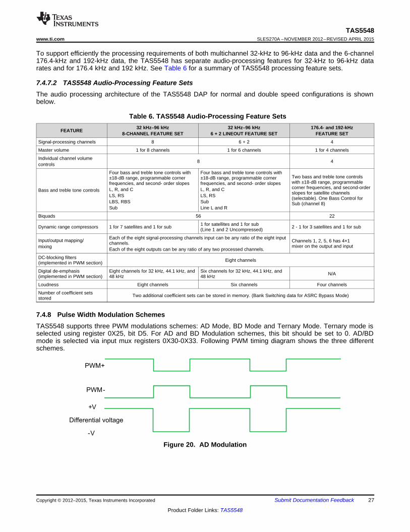
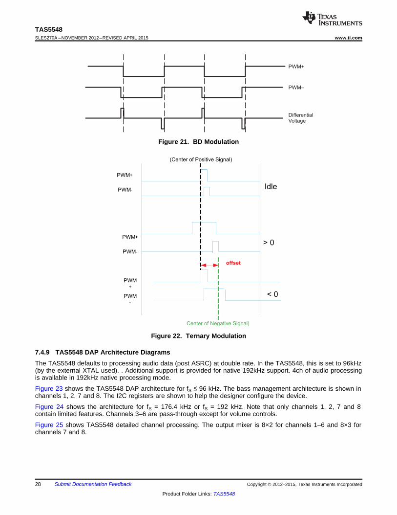
7.4.8 Pulse Width Modulation SchemesTAS5548 supports three PWM modulations schemes: AD Mode, BD Mode and Ternary Mode. Ternary mode isselected using register 0X25, bit D5. For AD and BD Modulation schemes, this bit should be set to 0. AD/BDmode is selected via input mux registers 0X30-0X33. Following PWM timing diagram shows the three differentschemes.
Figure 20. AD Modulation
Copyright © 2012–2015, Texas Instruments Incorporated Submit Documentation Feedback 27
Product Folder Links: TAS5548
PWM+
PWM-
PWM+
PWM-
> 0
Idle
Center of Negative Signal)
< 0
PWM
+
PWM
-
offset
(Center of Positive Signal)
PWM+
PWM–
DifferentialVoltage
TAS5548SLES270A –NOVEMBER 2012–REVISED APRIL 2015 www.ti.com
Figure 21. BD Modulation
Figure 22. Ternary Modulation
7.4.9 TAS5548 DAP Architecture DiagramsThe TAS5548 defaults to processing audio data (post ASRC) at double rate. In the TAS5548, this is set to 96kHz(by the external XTAL used). . Additional support is provided for native 192kHz support. 4ch of audio processingis available in 192kHz native processing mode.
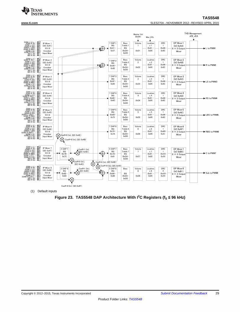
Figure 23 shows the TAS5548 DAP architecture for fS ≤ 96 kHz. The bass management architecture is shown inchannels 1, 2, 7 and 8. The I2C registers are shown to help the designer configure the device.
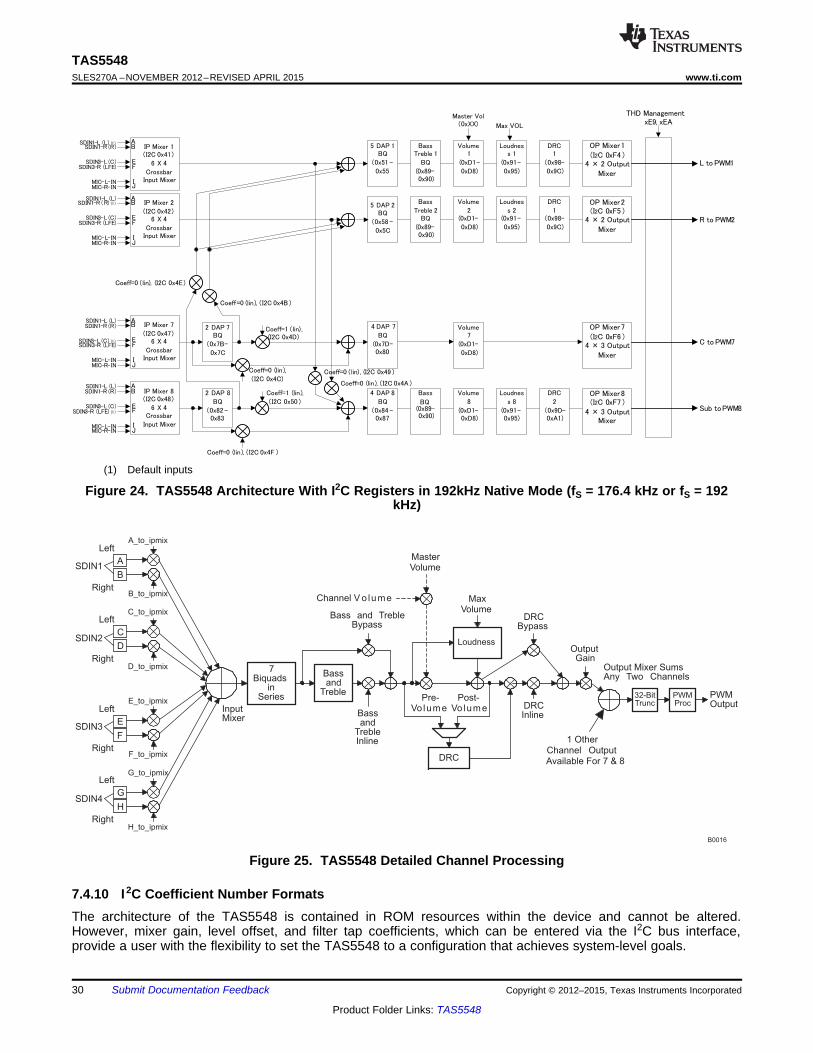
Figure 24 shows the architecture for fS = 176.4 kHz or fS = 192 kHz. Note that only channels 1, 2, 7 and 8contain limited features. Channels 3–6 are pass-through except for volume controls.
Figure 25 shows TAS5548 detailed channel processing. The output mixer is 8×2 for channels 1–6 and 8×3 forchannels 7 and 8.
28 Submit Documentation Feedback Copyright © 2012–2015, Texas Instruments Incorporated
Product Folder Links: TAS5548
IP Mixer 1(I2C 0x41 )
10 X 8
CrossbarInput Mixer
A
HGFEDCB
IJ
SDIN1-L (L)(1)SDIN1-R (R)
SDIN2-L (LS)SDIN2-R (RS)
SDIN3-L (LBS)SDIN3-R (RBS)
SDIN4-L (C)SDIN4-R (LFE)
MIC-L-INMIC-R-IN
IP Mixer 2
(I2C 0x42 )10 X 8
CrossbarInput Mixer
A
HGFEDCB
IJ
SDIN1-L (L)SDIN1-R (R)(1)
SDIN2-L (LS)SDIN2-R (RS)
SDIN3-L (LBS)SDIN3-R (RBS)
SDIN4-L (C)SDIN4-R (LFE)
MIC-L-INMIC-R-IN
IP Mixer 3
(I2C 0x43 )10 X 8
Crossbar
Input Mixer
A
HGFEDCB
IJ
SDIN1-L (L)SDIN1-R (R)
SDIN2-L (LS)(1)SDIN2-R (RS)
SDIN3-L (LBS)SDIN3-R (RBS)
SDIN4-L (C)SDIN4-R (LFE)
MIC-L-INMIC-R-IN
IP Mixer 4
(I2C 0x44 )
10 X 8Crossbar
Input Mixer
A
HGFEDCB
IJ
SDIN1-L (L)SDIN1-R (R)
SDIN2-L (LS)SDIN2-R (RS)(1)SDIN3-L (LBS)SDIN3-R (RBS)
SDIN4-L (C)SDIN4-R (LFE)
MIC-L-INMIC-R-IN
IP Mixer 5(I2C 0x45 )
10 X 8
CrossbarInput Mixer
A
HGFEDCB
IJ
SDIN1-L (L)SDIN1-R (R)
SDIN2-L (LS)SDIN2-R (RS)
SDIN3-L (LBS)(1)SDIN3-R (RBS)
SDIN4-L (C)SDIN4-R (LFE)
MIC-L-INMIC-R-IN
IP Mixer 6
(I2C 0x46 )10 X 8
CrossbarInput Mixer
A
HGFEDCB
IJ
SDIN1-L (L)SDIN1-R (R)
SDIN2-L (LS)SDIN2-R (RS)
SDIN3-L (LBS)SDIN3-R (RBS)(1)
SDIN4-L (C)SDIN4-R (LFE)
MIC-L-INMIC-R-IN
IP Mixer 7
(I2C 0x47 )10 X 8
Crossbar
Input Mixer
A
HGFEDCB
IJ
SDIN1-L (L)SDIN1-R (R)
SDIN2-L (LS)SDIN2-R (RS)
SDIN3-L (LBS)SDIN3-R (RBS)SDIN4-L (C)(1)SDIN4-R (LFE)
MIC-L-INMIC-R-IN
IP Mixer 8(I2C 0x48 )
10 X 8
CrossbarInput Mixer
A
HGFEDCB
IJ
SDIN1-L (L)SDIN1-R (R)
SDIN2-L (LS)SDIN2-R (RS)
SDIN3-L (LBS)SDIN3-R (RBS)
SDIN4-L (C)SDIN4-R (LFE)(1)
MIC-L-INMIC-R-IN
2 DAP 8BQ
(0x82 -0x83
2 DAP 7
BQ(0x7B-
0x7C
Coeff=0 (lin), (I2C 0x4F)
Coeff=0 (lin),
(I2C 0x4C)
Coeff=1 (lin),(I2C 0x50 )
Coeff=1 (lin),(I2C 0x4D)
Coeff=0 (lin), (I2C 0x4B)
Coeff=0 (lin), (I2C 0x4E)
Coeff=0 (lin), (I2C 0x4A)
Coeff=0 (lin), (I2C 0x49 )
7 DAP 1BQ
(0x51 -
0x57
7 DAP 2BQ
(0x58 -
0x5E
7 DAP 3
BQ(0x5F-
0x65
7 DAP 4BQ
(0x66 -0x6C
7 DAP 5BQ
(0x6D-
0x73
7 DAP 6
BQ(0x74 -
0x7A
5 DAP 7
BQ(0x7D-
0x81
5 DAP 8BQ
(0x84 -0x88
BassTreble 1
BQ
(0xDA-0xDD
Bass
Treble 2BQ
(0xDA-0xDD
Bass
Treble 3BQ
(0xDA-
0xDD
BassTreble 4
BQ(0xDA-
0xDD
BassTreble 5
BQ
(0xDA-0xDD
Bass
Treble 6BQ
(0xDA-0xDD
Bass
Treble 7BQ
(0xDA-0xDD
Bass
BQ(0xDA-
0xDD
Volume1
0xD1
Volume
2
0xD2
Volume
3
0xD3
Loudness 1
(0x91 -
0x95
OP Mixer1
(I C 0xAA)2
8 × 2 Output
Mixer
Volume4
0xD4
Volume5
0xD5
Volume
6
0xD6
Volume
7
0xD7
Volume8
0xD8
Loudnes
s 2(0x91 -
0x95
Loudnes
s 3(0x91 -
0x95
Loudness 4
(0x91 -0x95
Loudness 5
(0x91 -
0x95
Loudnes
s 6(0x91 -
0x95
Loudnes
s 7(0x91 -
0x95
Loudness 8
(0x91 -0x95
DRC1
(0x96 -
0x9C
DRC
1(0x96 -
0x9C
DRC
1(0x96 -
0x9C
DRC1
(0x96 -0x9C
DRC1
(0x96 -
0x9C
DRC
1(0x9D-
0xA1
DRC
1(0xXX-
0xXX
DRC2
(0xXX-0xXX
OP Mixer2(I C 0xAB)2
8 × 2 Output
Mixer
OP Mixer3(I C 0xAC)2
8 × 2 OutputMixer
OP Mixer4
(I C 0xAD)2
8 × 2 OutputMixer
OP Mixer5
(I C 0xAE)2
8 × 2 Output
Mixer
OP Mixer6(I C 0xAF)2
8 × 2 Output
Mixer
OP Mixer7(I C 0xB0)2
8 × 3 Output
Mixer
OP Mixer8
(I C 0xB1)2
8 × 3 OutputMixer
Master Vol(0xD9) Max VOL
THD ManagementxE9, xEA
L to PWM1
R to PWM2
LS toPWM3
RS to PWM4
LBS to PWM5
RBS to PWM6
C to PWM7
Sub toPWM8
TAS5548www.ti.com SLES270A –NOVEMBER 2012–REVISED APRIL 2015
(1) Default inputs
Figure 23. TAS5548 DAP Architecture With I2C Registers (fS ≤ 96 kHz)
Copyright © 2012–2015, Texas Instruments Incorporated Submit Documentation Feedback 29
Product Folder Links: TAS5548
7Biquads
inSeries
Bassand
Treble
Loudness
DRC
InputMixer
1 OtherChannel OutputAvailable For 7 & 8
32-BitTrunc
PWMProc
A_to_ipmix
B_to_ipmix
ASDIN1
B
C_to_ipmix
D_to_ipmix
SDIN2
Left
RightChannel V o lume
Bass and TrebleBypass
Bassand
TrebleInline
Pre-Vo lume
Post-Vo lume
OutputGain
Output Mixer SumsAny Two Channels
PWMOutput
C
D
Left
Right
DRCBypass
DRCInline
E_to_ipmix
F_to_ipmix
ESDIN3
F
G_to_ipmix
H_to_ipmix
SDIN4
Left
Right
G
H
Left
Right
B0016
MasterVolume
MaxVolume
IP Mixer 1(I2C 0x41)
6 X 4
CrossbarInput Mixer
A
FE
B
IJ
SDIN1-L (L) (1)SDIN1-R (R)
SDIN3-L (C)SDIN3-R (LFE)
MIC-L-INMIC-R-IN
IP Mixer 2
(I2C 0x42)6 X 4
CrossbarInput Mixer
A
FE
B
IJ
SDIN1-L (L)SDIN1-R (R) (1)
SDIN3-L (C)SDIN3-R (LFE)
MIC-L-INMIC-R-IN
IP Mixer 7
(I2C 0x47)6 X 4
CrossbarInput Mixer
A
FE
B
IJ
SDIN1-L (L)SDIN1-R (R)
SDIN3-L (C) (1)SDIN3-R (LFE)
MIC-L-INMIC-R-IN
IP Mixer 8(I2C 0x48)
6 X 4Crossbar
Input Mixer
A
FE
B
IJ
SDIN1-L (L)SDIN1-R (R)
SDIN3-L (C)SDIN3-R (LFE) (1)
MIC-L-INMIC-R-IN
2 DAP 8
BQ
(0x82 -0x83
2 DAP 7BQ
(0x7B-
0x7C
Coeff=0 (lin), (I2C 0x4F )
Coeff=0 (lin),
(I2C 0x4C)
Coeff=1 (lin),
(I2C 0x50 )
Coeff=1 (lin),(I2C 0x4D)
Coeff=0 (lin), (I2C 0x4B )
Coeff=0 (lin), (I2C 0x4E)
Coeff=0 (lin), (I2C 0x4A )
Coeff=0 (lin), (I2C 0x49 )
5 DAP 1BQ
(0x51 -
0x55
5 DAP 2BQ
(0x58 -
0x5C
4 DAP 8
BQ
(0x84 -0x87
BassTreble 1
BQ
(0x89-0x90)
Bass
Treble 2BQ
(0x89-0x90)
Bass
BQ(0x89-0x90)
Volume1
(0xD1-
0xD8)
Volume
2(0xD1-
0xD8)
Loudness 1
(0x91-
0x95)
OP Mixer1
(I C 0xF4 )2
4 × 2 Output
Mixer
Volume7
(0xD1-
0xD8)
Volume
8
(0xD1-0xD8)
Loudnes
s 2(0x91-
0x95)
Loudnes
s 8
(0x91-0x95)
DRC1
(0x98-
0x9C)
DRC
1(0x98-
0x9C)
DRC
2
(0x9D-0xA1)
OP Mixer2(I C 0xF5 )2
4 × 2 Output
Mixer
OP Mixer7
(I2C 0xF6 )4 × 3 Output
Mixer
OP Mixer8(I C 0xF7 )2
4 × 3 OutputMixer
Master Vol(0xXX) Max VOL
THD ManagementxE9, xEA
L to PWM1
R to PWM2
C to PWM7
Sub toPWM8
4 DAP
BQ
(0x7D-0x80
7
TAS5548SLES270A –NOVEMBER 2012–REVISED APRIL 2015 www.ti.com
(1) Default inputs
Figure 24. TAS5548 Architecture With I2C Registers in 192kHz Native Mode (fS = 176.4 kHz or fS = 192kHz)
Figure 25. TAS5548 Detailed Channel Processing
7.4.10 I2C Coefficient Number FormatsThe architecture of the TAS5548 is contained in ROM resources within the device and cannot be altered.However, mixer gain, level offset, and filter tap coefficients, which can be entered via the I2C bus interface,provide a user with the flexibility to set the TAS5548 to a configuration that achieves system-level goals.
30 Submit Documentation Feedback Copyright © 2012–2015, Texas Instruments Incorporated
Product Folder Links: TAS5548
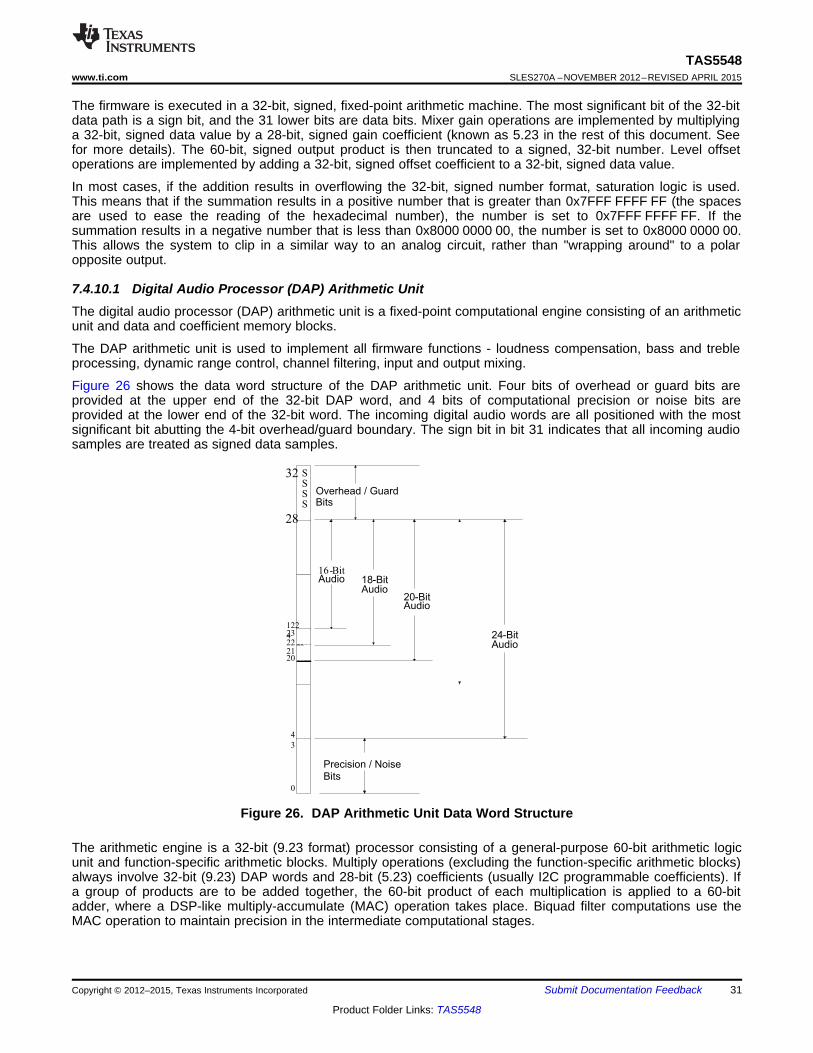
S
S
S
S
32
28
122
423
22
2120
4
3
0
Overhead / Guard
Bits
16-BitAudio 18-Bit
Audio20-BitAudio
24-BitAudio
Precision / Noise
Bits
TAS5548www.ti.com SLES270A –NOVEMBER 2012–REVISED APRIL 2015
The firmware is executed in a 32-bit, signed, fixed-point arithmetic machine. The most significant bit of the 32-bitdata path is a sign bit, and the 31 lower bits are data bits. Mixer gain operations are implemented by multiplyinga 32-bit, signed data value by a 28-bit, signed gain coefficient (known as 5.23 in the rest of this document. Seefor more details). The 60-bit, signed output product is then truncated to a signed, 32-bit number. Level offsetoperations are implemented by adding a 32-bit, signed offset coefficient to a 32-bit, signed data value.
In most cases, if the addition results in overflowing the 32-bit, signed number format, saturation logic is used.This means that if the summation results in a positive number that is greater than 0x7FFF FFFF FF (the spacesare used to ease the reading of the hexadecimal number), the number is set to 0x7FFF FFFF FF. If thesummation results in a negative number that is less than 0x8000 0000 00, the number is set to 0x8000 0000 00.This allows the system to clip in a similar way to an analog circuit, rather than "wrapping around" to a polaropposite output.
7.4.10.1 Digital Audio Processor (DAP) Arithmetic UnitThe digital audio processor (DAP) arithmetic unit is a fixed-point computational engine consisting of an arithmeticunit and data and coefficient memory blocks.
The DAP arithmetic unit is used to implement all firmware functions - loudness compensation, bass and trebleprocessing, dynamic range control, channel filtering, input and output mixing.
Figure 26 shows the data word structure of the DAP arithmetic unit. Four bits of overhead or guard bits areprovided at the upper end of the 32-bit DAP word, and 4 bits of computational precision or noise bits areprovided at the lower end of the 32-bit word. The incoming digital audio words are all positioned with the mostsignificant bit abutting the 4-bit overhead/guard boundary. The sign bit in bit 31 indicates that all incoming audiosamples are treated as signed data samples.
Figure 26. DAP Arithmetic Unit Data Word Structure
The arithmetic engine is a 32-bit (9.23 format) processor consisting of a general-purpose 60-bit arithmetic logicunit and function-specific arithmetic blocks. Multiply operations (excluding the function-specific arithmetic blocks)always involve 32-bit (9.23) DAP words and 28-bit (5.23) coefficients (usually I2C programmable coefficients). Ifa group of products are to be added together, the 60-bit product of each multiplication is applied to a 60-bitadder, where a DSP-like multiply-accumulate (MAC) operation takes place. Biquad filter computations use theMAC operation to maintain precision in the intermediate computational stages.
Copyright © 2012–2015, Texas Instruments Incorporated Submit Documentation Feedback 31
Product Folder Links: TAS5548
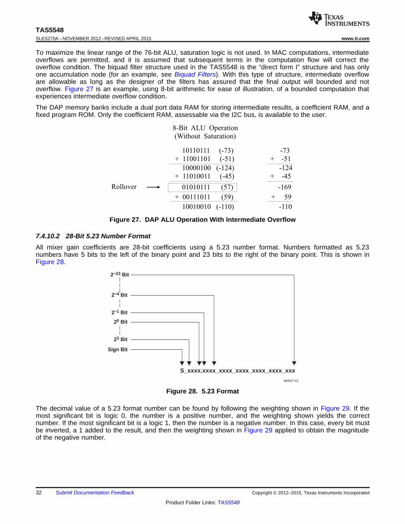
2−23 Bit
S_xxxx.xxxx_xxxx_xxxx_xxxx_xxxx_xxx
2−4 Bit
2−1 Bit
20 Bit
Sign Bit
23 Bit
M0007-01
10110111 (-73) -73
+ 11001101 (-51) + -51
10000100 (-124) -124
+ 11010011 (-45) + -45
01010111 (57) -169
+ 00111011 (59) + 59
10010010 (-110) -110
8-Bit ALU Operation
(Without Saturation)
Rollover
TAS5548SLES270A –NOVEMBER 2012–REVISED APRIL 2015 www.ti.com
To maximize the linear range of the 76-bit ALU, saturation logic is not used. In MAC computations, intermediateoverflows are permitted, and it is assumed that subsequent terms in the computation flow will correct theoverflow condition. The biquad filter structure used in the TAS5548 is the “direct form I” structure and has onlyone accumulation node (for an example, see Biquad Filters). With this type of structure, intermediate overfloware allowable as long as the designer of the filters has assured that the final output will bounded and notoverflow. Figure 27 is an example, using 8-bit arithmetic for ease of illustration, of a bounded computation thatexperiences intermediate overflow condition.
The DAP memory banks include a dual port data RAM for storing intermediate results, a coefficient RAM, and afixed program ROM. Only the coefficient RAM, assessable via the I2C bus, is available to the user.
Figure 27. DAP ALU Operation With Intermediate Overflow
7.4.10.2 28-Bit 5.23 Number FormatAll mixer gain coefficients are 28-bit coefficients using a 5.23 number format. Numbers formatted as 5.23numbers have 5 bits to the left of the binary point and 23 bits to the right of the binary point. This is shown inFigure 28.
Figure 28. 5.23 Format
The decimal value of a 5.23 format number can be found by following the weighting shown in Figure 29. If themost significant bit is logic 0, the number is a positive number, and the weighting shown yields the correctnumber. If the most significant bit is a logic 1, then the number is a negative number. In this case, every bit mustbe inverted, a 1 added to the result, and then the weighting shown in Figure 29 applied to obtain the magnitudeof the negative number.
32 Submit Documentation Feedback Copyright © 2012–2015, Texas Instruments Incorporated
Product Folder Links: TAS5548
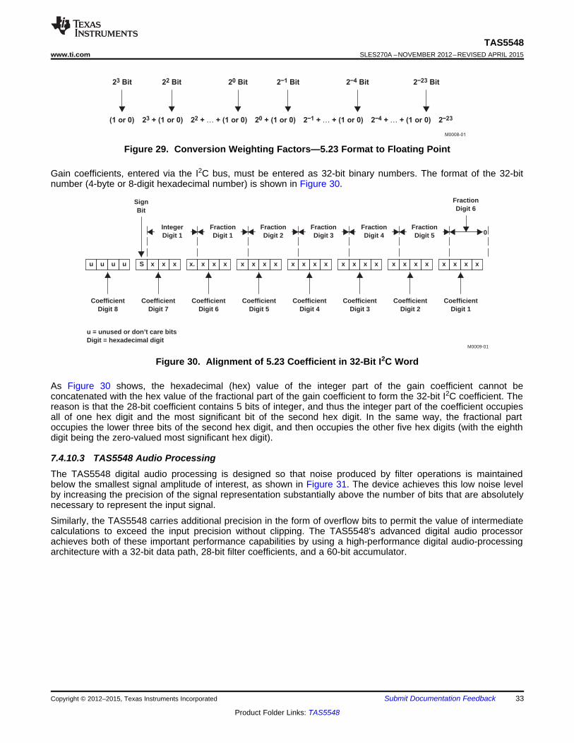
u
CoefficientDigit 8
u u u S x x x
CoefficientDigit 7
x. x x x
CoefficientDigit 6
x x x x
CoefficientDigit 5
x x x x
CoefficientDigit 4
x x x x
CoefficientDigit 3
x x x x
CoefficientDigit 2
x x x x
CoefficientDigit 1
FractionDigit 5
SignBit
0
FractionDigit 6
FractionDigit 4
FractionDigit 3
FractionDigit 2
FractionDigit 1
IntegerDigit 1
u = unused or don’t care bitsDigit = hexadecimal digit
M0009-01
(1 or 0) 23 + (1 or 0) 22 + … + (1 or 0) 20 + (1 or 0) 2−1 + … + (1 or 0) 2−4 + … + (1 or 0) 2−23
23 Bit 22 Bit 20 Bit 2−1 Bit 2−4 Bit 2−23 Bit
M0008-01
TAS5548www.ti.com SLES270A –NOVEMBER 2012–REVISED APRIL 2015
Figure 29. Conversion Weighting Factors—5.23 Format to Floating Point
Gain coefficients, entered via the I2C bus, must be entered as 32-bit binary numbers. The format of the 32-bitnumber (4-byte or 8-digit hexadecimal number) is shown in Figure 30.
Figure 30. Alignment of 5.23 Coefficient in 32-Bit I2C Word
As Figure 30 shows, the hexadecimal (hex) value of the integer part of the gain coefficient cannot beconcatenated with the hex value of the fractional part of the gain coefficient to form the 32-bit I2C coefficient. Thereason is that the 28-bit coefficient contains 5 bits of integer, and thus the integer part of the coefficient occupiesall of one hex digit and the most significant bit of the second hex digit. In the same way, the fractional partoccupies the lower three bits of the second hex digit, and then occupies the other five hex digits (with the eighthdigit being the zero-valued most significant hex digit).
7.4.10.3 TAS5548 Audio ProcessingThe TAS5548 digital audio processing is designed so that noise produced by filter operations is maintainedbelow the smallest signal amplitude of interest, as shown in Figure 31. The device achieves this low noise levelby increasing the precision of the signal representation substantially above the number of bits that are absolutelynecessary to represent the input signal.
Similarly, the TAS5548 carries additional precision in the form of overflow bits to permit the value of intermediatecalculations to exceed the input precision without clipping. The TAS5548's advanced digital audio processorachieves both of these important performance capabilities by using a high-performance digital audio-processingarchitecture with a 32-bit data path, 28-bit filter coefficients, and a 60-bit accumulator.
Copyright © 2012–2015, Texas Instruments Incorporated Submit Documentation Feedback 33
Product Folder Links: TAS5548
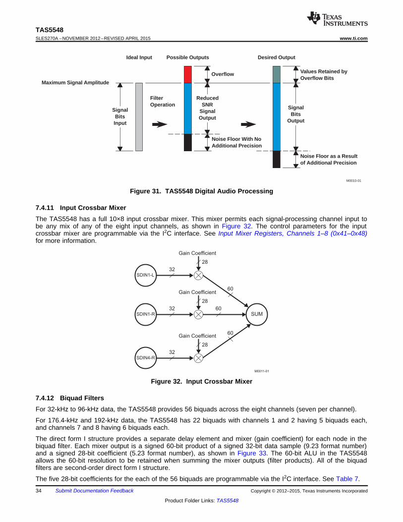
Gain Coefficient
32
SDIN1-L
28
60Gain Coefficient
32
28
60
SUM
Gain Coefficient
32
28
60
M0011-01
SDIN1-R
SDIN4-R
Noise Floor With NoAdditional Precision
Maximum Signal Amplitude
Ideal Input Possible Outputs Desired Output
FilterOperation
SignalBitsInput
Overflow
ReducedSNR
SignalOutput
Noise Floor as a Resultof Additional Precision
SignalBits
Output
Values Retained byOverflow Bits
M0010-01
TAS5548SLES270A –NOVEMBER 2012–REVISED APRIL 2015 www.ti.com
Figure 31. TAS5548 Digital Audio Processing
7.4.11 Input Crossbar MixerThe TAS5548 has a full 10×8 input crossbar mixer. This mixer permits each signal-processing channel input tobe any mix of any of the eight input channels, as shown in Figure 32. The control parameters for the inputcrossbar mixer are programmable via the I2C interface. See Input Mixer Registers, Channels 1–8 (0x41–0x48)for more information.
Figure 32. Input Crossbar Mixer
7.4.12 Biquad FiltersFor 32-kHz to 96-kHz data, the TAS5548 provides 56 biquads across the eight channels (seven per channel).
For 176.4-kHz and 192-kHz data, the TAS5548 has 22 biquads with channels 1 and 2 having 5 biquads each,and channels 7 and 8 having 6 biquads each.
The direct form I structure provides a separate delay element and mixer (gain coefficient) for each node in thebiquad filter. Each mixer output is a signed 60-bit product of a signed 32-bit data sample (9.23 format number)and a signed 28-bit coefficient (5.23 format number), as shown in Figure 33. The 60-bit ALU in the TAS5548allows the 60-bit resolution to be retained when summing the mixer outputs (filter products). All of the biquadfilters are second-order direct form I structure.
The five 28-bit coefficients for the each of the 56 biquads are programmable via the I2C interface. See Table 7.
34 Submit Documentation Feedback Copyright © 2012–2015, Texas Instruments Incorporated
Product Folder Links: TAS5548
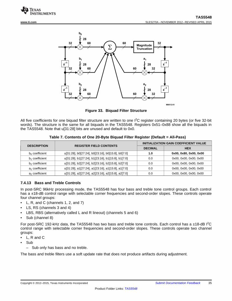
28
32 60 32
b0
28
32 60
b1
S
28
32 60
b2
60
28
60 32
a1
28
60 32
a2
M0012-01
z–1
z–1
MagnitudeTruncation
z–1
z–1
TAS5548www.ti.com SLES270A –NOVEMBER 2012–REVISED APRIL 2015
Figure 33. Biquad Filter Structure
All five coefficients for one biquad filter structure are written to one I2C register containing 20 bytes (or five 32-bitwords). The structure is the same for all biquads in the TAS5548. Registers 0x51–0x88 show all the biquads inthe TAS5548. Note that u[31:28] bits are unused and default to 0x0.
Table 7. Contents of One 20-Byte Biquad Filter Register (Default = All-Pass)INITIALIZATION GAIN COEFFICIENT VALUE
DESCRIPTION REGISTER FIELD CONTENTSDECIMAL HEX
b0 coefficient u[31:28], b0[27:24], b0[23:16], b0[15:8], b0[7:0] 1.0 0x00, 0x80, 0x00, 0x00b1 coefficient u[31:28], b1[27:24], b1[23:16], b1[15:8], b1[7:0] 0.0 0x00, 0x00, 0x00, 0x00b2 coefficient u[31:28], b2[27:24], b2[23:16], b2[15:8], b2[7:0] 0.0 0x00, 0x00, 0x00, 0x00a1 coefficient u[31:28], a1[27:24], a1[23:16], a1[15:8], a1[7:0] 0.0 0x00, 0x00, 0x00, 0x00a2 coefficient u[31:28], a2[27:24], a2[23:16], a2[15:8], a2[7:0] 0.0 0x00, 0x00, 0x00, 0x00
7.4.13 Bass and Treble ControlsIn post-SRC 96kHz processing mode, the TAS5548 has four bass and treble tone control groups. Each controlhas a ±18-dB control range with selectable corner frequencies and second-order slopes. These controls operatefour channel groups:• L, R, and C (channels 1, 2, and 7)• LS, RS (channels 3 and 4)• LBS, RBS (alternatively called L and R lineout) (channels 5 and 6)• Sub (channel 8)
For post-SRC 192-kHz data, the TAS5548 has two bass and treble tone controls. Each control has a ±18-dB I2Ccontrol range with selectable corner frequencies and second-order slopes. These controls operate two channelgroups:• L, R and C• Sub
– Sub only has bass and no treble.
The bass and treble filters use a soft update rate that does not produce artifacts during adjustment.
Copyright © 2012–2015, Texas Instruments Incorporated Submit Documentation Feedback 35
Product Folder Links: TAS5548
TAS5548SLES270A –NOVEMBER 2012–REVISED APRIL 2015 www.ti.com
Table 8. Bass and Treble Filter Selections3-dB CORNER FREQUENCIES, Hz
fS FILTER SET 1 FILTER SET 2 FILTER SET 3 FILTER SET 4 FILTER SET 5(kHz)BASS TREBLE BASS TREBLE BASS TREBLE BASS TREBLE BASS TREBLE
88.2 115 2527 230 5053 345 8269 402 10106 459 1194496 125 2750 250 5500 375 9000 438 11000 500 13000
176.4 230 5053 459 10106 689 16538 804 20213 919 23888192 250 5500 500 11000 750 18000 875 22000 1000 26000
The I2C registers that control bass and treble are:• Bass and treble bypass register (0x89–0x90, channels 1–8)• Bass and treble slew rates (0xD0)• Bass filter sets 1–5 (0xDA)• Bass filter index (0xDB)• Treble filter sets 1–5 (0xDC)• Treble filter index (0xDD)
NOTEThe bass and treble bypass registers (0x89–0x90) are defaulted to the bypass mode. Inorder to use the bass and treble, these registers must be in the inline (or enabled) modefor each channel using bass and treble.
7.4.14 Volume, Automute, and MuteThe TAS5548 provides individual channel and master volume controls. Each control provides an adjustmentrange of 18 dB to –127 dB in 0.25-dB increments. This permits a total volume device control range of 36 dB to–127 dB plus mute. The master volume control can be configured to control six or eight channels.
The TAS5548 has a master soft mute control that can be enabled by a terminal or I2C command. The devicealso has individual channel soft mute controls that are enabled via I2C.
7.4.15 Loudness CompensationThe loudness compensation function compensates for the Fletcher-Munson loudness curves. The TAS5548loudness implementation tracks the volume control setting to provide spectral compensation for weak low- orhigh-frequency response at low volume levels. For the volume tracking function, both linear and logarithmiccontrol laws can be implemented. Any biquad filter response can be used to provide the desired loudness curve.The control parameters for the loudness control are programmable via the I2C interface.
The TAS5548 has a single set of loudness controls for the eight channels. In 6-channel mode, loudness isavailable to the six speaker outputs and also to the line outputs. The loudness control input uses the maximumindividual master volume (V) to control the loudness that is applied to all channels. In the 192-kHz and 176.4-kHzmodes, the loudness function is active only for channels 1, 2, and 8.
36 Submit Documentation Feedback Copyright © 2012–2015, Texas Instruments Incorporated
Product Folder Links: TAS5548
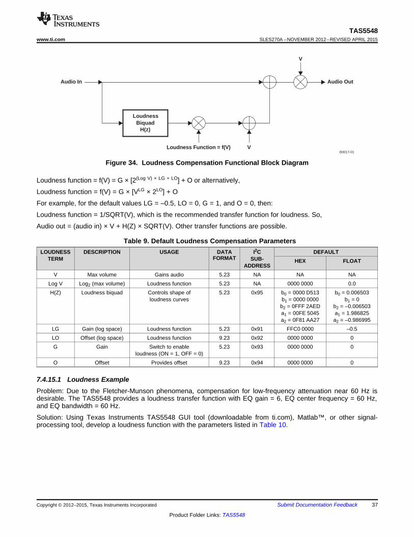
B0017-01
LoudnessBiquad
H(z)
Audio OutAudio In
V
VLoudness Function = f(V)
TAS5548www.ti.com SLES270A –NOVEMBER 2012–REVISED APRIL 2015
Figure 34. Loudness Compensation Functional Block Diagram
Loudness function = f(V) = G × [2(Log V) × LG + LO] + O or alternatively,
Loudness function = f(V) = G × [VLG × 2LO] + O
For example, for the default values LG = –0.5, LO = 0, G = 1, and O = 0, then:
Loudness function = 1/SQRT(V), which is the recommended transfer function for loudness. So,
Audio out = (audio in) × V + H(Z) × SQRT(V). Other transfer functions are possible.
Table 9. Default Loudness Compensation ParametersLOUDNESS DESCRIPTION USAGE DATA I2C DEFAULT
FORMATTERM SUB- HEX FLOATADDRESS
V Max volume Gains audio 5.23 NA NA NALog V Log2 (max volume) Loudness function 5.23 NA 0000 0000 0.0H(Z) Loudness biquad Controls shape of 5.23 0x95 b0 = 0000 D513 b0 = 0.006503
loudness curves b1 = 0000 0000 b1 = 0b2 = 0FFF 2AED b2 = –0.006503a1 = 00FE 5045 a1 = 1.986825a2 = 0F81 AA27 a2 = –0.986995
LG Gain (log space) Loudness function 5.23 0x91 FFC0 0000 –0.5LO Offset (log space) Loudness function 9.23 0x92 0000 0000 0G Gain Switch to enable 5.23 0x93 0000 0000 0
loudness (ON = 1, OFF = 0)O Offset Provides offset 9.23 0x94 0000 0000 0
7.4.15.1 Loudness ExampleProblem: Due to the Fletcher-Munson phenomena, compensation for low-frequency attenuation near 60 Hz isdesirable. The TAS5548 provides a loudness transfer function with EQ gain = 6, EQ center frequency = 60 Hz,and EQ bandwidth = 60 Hz.
Solution: Using Texas Instruments TAS5548 GUI tool (downloadable from ti.com), Matlab™, or other signal-processing tool, develop a loudness function with the parameters listed in Table 10.
Copyright © 2012–2015, Texas Instruments Incorporated Submit Documentation Feedback 37
Product Folder Links: TAS5548
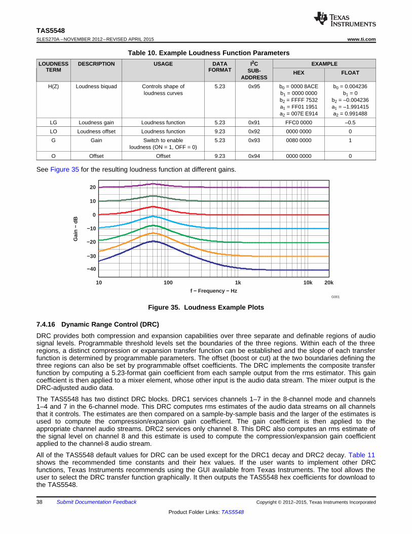
f − Frequency − Hz
Gai
n −
dB
10 20k100 1k
G001
20
0
−10
−20
−40
10
−30
10k
TAS5548SLES270A –NOVEMBER 2012–REVISED APRIL 2015 www.ti.com
Table 10. Example Loudness Function ParametersLOUDNESS DESCRIPTION USAGE DATA I2C EXAMPLE
TERM FORMAT SUB- HEX FLOATADDRESS
H(Z) Loudness biquad Controls shape of 5.23 0x95 b0 = 0000 8ACE b0 = 0.004236loudness curves b1 = 0000 0000 b1 = 0
b2 = FFFF 7532 b2 = –0.004236a1 = FF01 1951 a1 = –1.991415a2 = 007E E914 a2 = 0.991488
LG Loudness gain Loudness function 5.23 0x91 FFC0 0000 –0.5LO Loudness offset Loudness function 9.23 0x92 0000 0000 0G Gain Switch to enable 5.23 0x93 0080 0000 1
loudness (ON = 1, OFF = 0)O Offset Offset 9.23 0x94 0000 0000 0
See Figure 35 for the resulting loudness function at different gains.
Figure 35. Loudness Example Plots
7.4.16 Dynamic Range Control (DRC)DRC provides both compression and expansion capabilities over three separate and definable regions of audiosignal levels. Programmable threshold levels set the boundaries of the three regions. Within each of the threeregions, a distinct compression or expansion transfer function can be established and the slope of each transferfunction is determined by programmable parameters. The offset (boost or cut) at the two boundaries defining thethree regions can also be set by programmable offset coefficients. The DRC implements the composite transferfunction by computing a 5.23-format gain coefficient from each sample output from the rms estimator. This gaincoefficient is then applied to a mixer element, whose other input is the audio data stream. The mixer output is theDRC-adjusted audio data.
The TAS5548 has two distinct DRC blocks. DRC1 services channels 1–7 in the 8-channel mode and channels1–4 and 7 in the 6-channel mode. This DRC computes rms estimates of the audio data streams on all channelsthat it controls. The estimates are then compared on a sample-by-sample basis and the larger of the estimates isused to compute the compression/expansion gain coefficient. The gain coefficient is then applied to theappropriate channel audio streams. DRC2 services only channel 8. This DRC also computes an rms estimate ofthe signal level on channel 8 and this estimate is used to compute the compression/expansion gain coefficientapplied to the channel-8 audio stream.
All of the TAS5548 default values for DRC can be used except for the DRC1 decay and DRC2 decay. Table 11shows the recommended time constants and their hex values. If the user wants to implement other DRCfunctions, Texas Instruments recommends using the GUI available from Texas Instruments. The tool allows theuser to select the DRC transfer function graphically. It then outputs the TAS5548 hex coefficients for download tothe TAS5548.
38 Submit Documentation Feedback Copyright © 2012–2015, Texas Instruments Incorporated
Product Folder Links: TAS5548
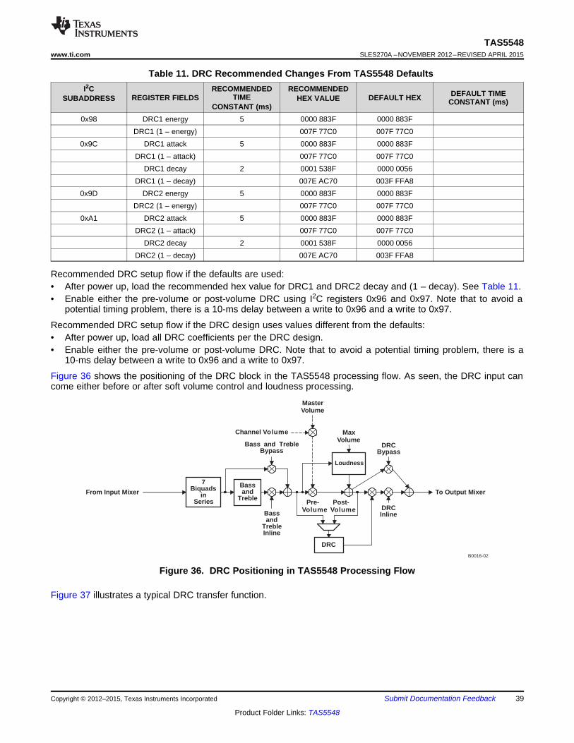
7Biquads
inSeries
Bassand
Treble
DRC
Bass and TrebleBypass
Bassand
TrebleInline
Pre-Volume
Post-Volume
DRCBypass
DRCInline
B0016-02
From Input Mixer To Output Mixer
Loudness
Channel V olume
MasterVolume
MaxVolume
TAS5548www.ti.com SLES270A –NOVEMBER 2012–REVISED APRIL 2015
Table 11. DRC Recommended Changes From TAS5548 DefaultsI2C RECOMMENDED RECOMMENDED DEFAULT TIMETIMEREGISTER FIELDS DEFAULT HEXSUBADDRESS HEX VALUE CONSTANT (ms)CONSTANT (ms)
0x98 DRC1 energy 5 0000 883F 0000 883FDRC1 (1 – energy) 007F 77C0 007F 77C0
0x9C DRC1 attack 5 0000 883F 0000 883FDRC1 (1 – attack) 007F 77C0 007F 77C0
DRC1 decay 2 0001 538F 0000 0056DRC1 (1 – decay) 007E AC70 003F FFA8
0x9D DRC2 energy 5 0000 883F 0000 883FDRC2 (1 – energy) 007F 77C0 007F 77C0
0xA1 DRC2 attack 5 0000 883F 0000 883FDRC2 (1 – attack) 007F 77C0 007F 77C0
DRC2 decay 2 0001 538F 0000 0056DRC2 (1 – decay) 007E AC70 003F FFA8
Recommended DRC setup flow if the defaults are used:• After power up, load the recommended hex value for DRC1 and DRC2 decay and (1 – decay). See Table 11.• Enable either the pre-volume or post-volume DRC using I2C registers 0x96 and 0x97. Note that to avoid a
potential timing problem, there is a 10-ms delay between a write to 0x96 and a write to 0x97.
Recommended DRC setup flow if the DRC design uses values different from the defaults:• After power up, load all DRC coefficients per the DRC design.• Enable either the pre-volume or post-volume DRC. Note that to avoid a potential timing problem, there is a
10-ms delay between a write to 0x96 and a write to 0x97.
Figure 36 shows the positioning of the DRC block in the TAS5548 processing flow. As seen, the DRC input cancome either before or after soft volume control and loudness processing.
Figure 36. DRC Positioning in TAS5548 Processing Flow
Figure 37 illustrates a typical DRC transfer function.
Copyright © 2012–2015, Texas Instruments Incorporated Submit Documentation Feedback 39
Product Folder Links: TAS5548
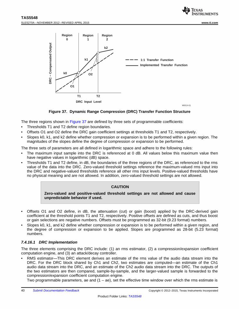
k2
T2
k1
k0
T1
O1
O2
DRC Input Level
DR
C −
Com
pens
ated
Out
put
1:1 Transfer Function
Implemented T ransfer Function
Region0
Region1
Region2
M0014-01
TAS5548SLES270A –NOVEMBER 2012–REVISED APRIL 2015 www.ti.com
Figure 37. Dynamic Range Compression (DRC) Transfer Function Structure
The three regions shown in Figure 37 are defined by three sets of programmable coefficients:• Thresholds T1 and T2 define region boundaries.• Offsets O1 and O2 define the DRC gain coefficient settings at thresholds T1 and T2, respectively.• Slopes k0, k1, and k2 define whether compression or expansion is to be performed within a given region. The
magnitudes of the slopes define the degree of compression or expansion to be performed.
The three sets of parameters are all defined in logarithmic space and adhere to the following rules:• The maximum input sample into the DRC is referenced at 0 dB. All values below this maximum value then
have negative values in logarithmic (dB) space.• Thresholds T1 and T2 define, in dB, the boundaries of the three regions of the DRC, as referenced to the rms
value of the data into the DRC. Zero-valued threshold settings reference the maximum-valued rms input intothe DRC and negative-valued thresholds reference all other rms input levels. Positive-valued thresholds haveno physical meaning and are not allowed. In addition, zero-valued threshold settings are not allowed.
CAUTIONZero-valued and positive-valued threshold settings are not allowed and causeunpredictable behavior if used.
• Offsets O1 and O2 define, in dB, the attenuation (cut) or gain (boost) applied by the DRC-derived gaincoefficient at the threshold points T1 and T2, respectively. Positive offsets are defined as cuts, and thus boostor gain selections are negative numbers. Offsets must be programmed as 32-bit (9.23 format) numbers.
• Slopes k0, k1, and k2 define whether compression or expansion is to be performed within a given region, andthe degree of compression or expansion to be applied. Slopes are programmed as 28-bit (5.23 format)numbers.
7.4.16.1 DRC ImplementationThe three elements comprising the DRC include: (1) an rms estimator, (2) a compression/expansion coefficientcomputation engine, and (3) an attack/decay controller.• RMS estimator—This DRC element derives an estimate of the rms value of the audio data stream into the
DRC. For the DRC block shared by Ch1 and Ch2, two estimates are computed—an estimate of the Ch1audio data stream into the DRC, and an estimate of the Ch2 audio data stream into the DRC. The outputs ofthe two estimators are then compared, sample-by-sample, and the larger-valued sample is forwarded to thecompression/expansion coefficient computation engine.Two programmable parameters, ae and (1 – ae), set the effective time window over which the rms estimate is
40 Submit Documentation Feedback Copyright © 2012–2015, Texas Instruments Incorporated
Product Folder Links: TAS5548
O1No Discontinuity
|T1 T2| k1 O2 For ( |T1| |T2| )= – × + ≥
ta1
fS
n(1 aa)td
1fS
n(1 ad)=
–
l –=
––l
twindow1
fS
n(1 ae)=
–
–l
TAS5548www.ti.com SLES270A –NOVEMBER 2012–REVISED APRIL 2015
made. For the DRC block shared by Ch1 and Ch2, the programmable parameters apply to both rmsestimators. The time window over which the rms estimation is computed can be determined by:
A. Care should be taken when calculating the time window for 192kHz content. Please use 96kHz as thesampling frequency for 96kHz AND 192kHz, as the TAS5548 uses a digital decimator to do all DAP processingat 96kHz.
B. ae = energy time (1)
• Compression/expansion coefficient computation—This DRC element converts the output of the rms estimatorto a logarithmic number, determines the region where the input resides, and then computes and outputs theappropriate coefficient to the attack/decay element. Seven programmable parameters, T1, T2, O1, O2, k0, k1,and k2, define the three compression/expansion regions implemented by this element.
• Attack/decay control—This DRC element controls the transition time of changes in the coefficient computed inthe compression/expansion coefficient computation element. Four programmable parameters define theoperation of this element. Parameters ad and (1 – ad) set the decay or release time constant to be used forvolume boost (expansion). Parameters aa and (1 – aa) set the attack time constant to be used for volumecuts. The transition time constants can be determined by:
C. aa = attack timeD. ad - decay time (2)
7.4.16.2 Compression/Expansion Coefficient Computation Engine ParametersSeven programmable parameters are assigned to each DRC block: two threshold parameters—T1 and T2, twooffset parameters—O1 and O2, and three slope parameters—k0, k1, and k2. The threshold parameters establishthe three regions of the DRC transfer curve, the offsets anchor the transfer curve by establishing known gainsettings at the threshold levels, and the slope parameters define whether a given region is a compression or anexpansion region.
T2 establishes the boundary between the high-volume region and the mid-volume region. T1 establishes theboundary between the mid-volume region and the low-volume region. Both thresholds are set in logarithmicspace, and which region is active for any given rms estimator output sample is determined by the logarithmicvalue of the sample.
Threshold T2 serves as the fulcrum or pivot point in the DRC transfer function. O2 defines the boost (> 0 dB) orcut (< 0 dB) implemented by the DRC-derived gain coefficient for an rms input level of T2. If O2 = 0 dB, the valueof the derived gain coefficient is 1 (0x0080 0000 in 5.23 format). k2 is the slope of the DRC transfer function forrms input levels above T2, and k1 is the slope of the DRC transfer function for rms input levels below T2 (andabove T1). The labeling of T2 as the fulcrum stems from the fact that there cannot be a discontinuity in thetransfer function at T2. The user can, however, set the DRC parameters to realize a discontinuity in the transferfunction at the boundary defined by T1. If no discontinuity is desired at T1, the value for the offset term O1 mustobey the following equation.
(3)
T1 and T2 are the threshold settings in dB, k1 is the slope for region 1, and O2 is the offset in dB at T2. If theuser chooses to select a value of O1 that does not obey the above equation, a ×discontinuity at T1 is realized.
Decreasing in volume from T2, the slope k1 remains in effect until the input level T1 is reached. If, at this inputlevel, the offset of the transfer function curve from the 1 : 1 transfer curve does not equal O1, there is adiscontinuity at this input level as the transfer function is snapped to the offset called for by O1. If no discontinuityis wanted, O1 and/or k1 must be adjusted so that the value of the transfer curve at input level T1 is offset fromthe 1 : 1 transfer curve by the value O1. The examples that follow illustrate both continuous and discontinuoustransfer curves at T1.
Decreasing in volume from T1, starting at offset level O1, slope k0 defines the compression/expansion activity inthe lower region of the DRC transfer curve.
Copyright © 2012–2015, Texas Instruments Incorporated Submit Documentation Feedback 41
Product Folder Links: TAS5548
0.5 : 1 compression k 10.5
1 1
1 : 2 expansion k 2 1 1
→
→
= – =
= – =
k1
n1= –
k1
n1= –
O1INPUT
–21 dB 24.0824 dB6.0206
0.51197555
0.1000_0011_0001_1101_0100
0x0041886A in 9.23 format
OINPUT
ODESIRED
24.0824 dB
6.0206=
+
T1SUB_ADDRESS_ENTRY
646.0206
10.63=–
–=
TAS5548SLES270A –NOVEMBER 2012–REVISED APRIL 2015 www.ti.com
7.4.16.2.1 Threshold Parameter Computation
For thresholds,
TdB = –6.0206TINPUT= –6.0206TSUB_ADDRESS_ENTRY
If, for example, it is desired to set T1 = –64 dB, then the subaddress entry required to set T1 to –64 dB is:
T1 is entered as a 32-bit number in 9.23 format. Therefore:
T1 = 10.63 = 0 1010.1010 0001 0100 0111 1010 111= 0x0550 A3D7 in 9.23 format
7.4.16.2.2 Offset Parameter Computation
The offsets set the boost or cut applied by the DRC-derived gain coefficient at the threshold point. An equivalentstatement is that offsets represent the departure of the actual transfer function from a 1 : 1 transfer at thethreshold point. Offsets are 9.23 Formatted, 32bit logarithmic numbers. They are computed by the followingequation:
Gains or boosts are represented as negative numbers; cuts or attenuations are represented as positive numbers.For example, to achieve a boost of 21 dB at threshold T1, the I2C coefficient value entered for O1 must be:
7.4.16.2.3 Slope Parameter Computation
In developing the equations used to determine the subaddress of the input value required to realize a givencompression or expansion within a given region of the DRC, the following convention is adopted.
DRC transfer = Input increase : Output increase
If the DRC realizes an output increase of n dB for every dB increase in the rms value of the audio into the DRC,a 1 : n expansion is being performed. If the DRC realizes a 1-dB increase in output level for every n-dB increasein the rms value of the audio into the DRC, an n : 1 compression is being performed.
k = n – 1
For n : 1 compression, the slope k can be found by:
In both expansion (1 : n) and compression (n : 1), n is implied to be greater than 1. Thus, for expansion:
k = n – 1 means k > 0 for n > 1. Likewise, for compression, means –1 < k < 0 for n > 1. Thus, itappears that k must always lie in the range k > –1.
The DRC imposes no such restriction and k can be programmed to values as negative as –15.999. To determinewhat results when such values of k are entered, it is first helpful to note that the compression and expansionequations for k are actually the same equation. For example, a 1 : 2 expansion is also a 0.5 : 1 compression.
42 Submit Documentation Feedback Copyright © 2012–2015, Texas Instruments Incorporated
Product Folder Links: TAS5548
Compression equation: k –4 1n 1 n 1
3–0.3333 : 1 compression
Expansion equation: k –4 n 1 n 3 1 : –3 expansion
=
=
= – →
→
= – →
= – = – →
TAS5548www.ti.com SLES270A –NOVEMBER 2012–REVISED APRIL 2015
As can be seen, the same value for k is obtained either way. The ability to choose values of k less than –1allows the DRC to implement negative-slope transfer curves within a given region. Negative-slope transfer curvesare usually not associated with compression and expansion operations, but the definition of these operations canbe expanded to include negative-slope transfer functions. For example, if k = –4
With k = –4, the output decreases 3 dB for every 1 dB increase in the rms value of the audio into the DRC. Asthe input increases in volume, the output decreases in volume.
7.4.17 THD ManagerThe THD manager is designed to set the max output level target after all processing has been completed. TheAudio clip engages at +24dB between (pre) and (post) stage. 10% distortion occurs when audio is clippingapprox +2.4 to 3dB over full scale. There is amplitude loss when clipping, so THD(post) might allow slight gainthrough THD manager. 10% distortion clipping will account for approx -1dB of output level loss. This is accountedfor as seen with +1dB in step 2 to set output level +0dB
Example setup to modify 10% THD output level: * note that coefficient calculations are approximate for simplicity1. Signal path settings
– Input -10dBFS– Volume 0xD9 0000 000C +15dB– THD Manager (pre) 0xE9 0650 0000 +22dB– THD Manager (post) 0xEA 0006 7000 -26dB
2. resulting output– output clipping at 10% distortion with output level +0dB– input -10 vol +15 THD(pre) +22 THD(post) -26– -10 +5 +27(clip) +1
3. Begin clipping at -12dBFS input with +0dB output level– THD Manager (pre) 0xE9 07FF FFFF +24dB (previous setting +22dB + 2dB)– result: input -12dBFS output clipping at 10% distortion with output level +0dB– input -12 vol +15 THD(pre) +24 THD(post) -26– -12 +3 +27(clip) +1
4. Begin clipping at -12dBFS input with -10dB output– THD Manager (post) 0xEA 0002 0000 -36dB (previous setting -26dB -10dB)– result: input -12dBFS output clipping at 10% distortion with output level +0dB– input -12 vol +15 THD(pre) +24 THD(post) -36– -12 +3 +27(clip) -9
Copyright © 2012–2015, Texas Instruments Incorporated Submit Documentation Feedback 43
Product Folder Links: TAS5548
( )
( )
L 0.707 C 0.707 Ls 0.707 RsL _ out
3.121
R 0.707 C 0.707 Ls 0.707 RsR _ out
3.121
+ ´ - ´ - ´=
+ ´ - ´ - ´=
L _ out E3 L E4 C E7 Ls E8 Rs
R _ out E3 R E4 C E5 Ls E6 Rs
= ´ + ´ + ´ + ´
= ´ + ´ + ´ + ´
LEFT
CH
RIGHT
CH
CENTER
CH
RIGHT
OUT
SDIN1COEF
0XE3
RS
CH
LS
CH
DOLBY
DOWN
MIX
COEF
0XE4
COEF
0XE5
COEF
0XE6
COEF
0XE8
COEF
0XE7
SDIN4
SDIN2
LEFT
OUT
TAS5548SLES270A –NOVEMBER 2012–REVISED APRIL 2015 www.ti.com
7.4.18 Downmix Algorithm and I2S Out
Figure 38. Dolby Downmix
The TAS5548 has an excellent feature that can mix the input signals to create a downmix to make the I2S serialoutput which has an SRC that keeps output sample rate at 48KHz irrespective of input sample rate.
Downmix registers are defined as follows:
0xE3 == Coefficient for L and R channels0xE4 == Coefficient for Center channel0xE5 == Coefficient for LS for R_out0xE6 == Coefficient for Rs for R_out0xE7 == Coefficient for Ls for L_out0xE8 == Coefficient for Rs for L_out
L, R, C, Ls, Rs are input cross bar mixer outputs. L, R, C, Ls, Rs are defined as the output of input mixers. L =Ch1, R = Ch2, C = Ch8, Ls = Ch3, Rs = Ch4, use input mixer to mix any other channels to I2S Out. (4)
Input Mixers also can be used as other mixers to mix subwoofer channels to I2S out.
By default I2S out has the following values:
test (5)
7.4.19 Stereo Downmixes/(or Fold-Downs)
7.4.19.1 Left Total/Right Total (Lt/Rt)Lt/Rt is a downmix suitable for decoding with a Dolby Pro Logic upmixer to obtain 5.1 channels again. Lt/Rt isalso suitable for stereophonic sound playback on a hi-fi or on headphones.
44 Submit Documentation Feedback Copyright © 2012–2015, Texas Instruments Incorporated
Product Folder Links: TAS5548
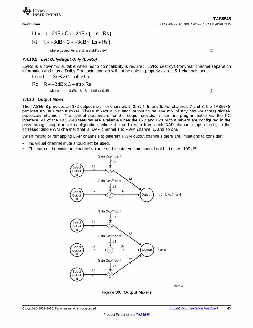
Gain Coefficient
32Select
Output
N
28
32Gain Coefficient
32
28
32Output
Select
Output
N
1, 2, 3, 4, 5, or 6
Gain Coefficient
32Select
Output
N
28
32Gain Coefficient
32
28
32Output
Select
Output
N
7 or 8
32Gain Coefficient
32Select
Output
N
28
M0011-05
Lo L 3dB C att Ls
Ro R 3dB C att Rs
= + - ´ + ´
= + - ´ + ´
( )
( )
Lt L 3dB C 3dB Ls Rs
Rt R 3dB C 3dB Ls Rs
= + - ´ + - ´ - -
= + - ´ + - ´ +
TAS5548www.ti.com SLES270A –NOVEMBER 2012–REVISED APRIL 2015
where Ls and Rs are phase shifted 90° (6)
7.4.19.2 Left Only/Right Only (Lo/Ro)Lo/Ro is a downmix suitable when mono compatibility is required. Lo/Ro destroys front/rear channel separationinformation and thus a Dolby Pro Logic upmixer will not be able to properly extract 5.1 channels again.
where att = –3 dB, –6 dB, –9 dB or 0 dB (7)
7.4.20 Output MixerThe TAS5548 provides an 8×2 output mixer for channels 1, 2, 3, 4, 5, and 6. For channels 7 and 8, the TAS5548provides an 8×3 output mixer. These mixers allow each output to be any mix of any two (or three) signal-processed channels. The control parameters for the output crossbar mixer are programmable via the I2Cinterface. All of the TAS5548 features are available when the 8×2 and 8×3 output mixers are configured in thepass-through output mixer configuration, where the audio data from each DAP channel maps directly to thecorresponding PWM channel (that is, DAP channel 1 to PWM channel 1, and so on).
When mixing or remapping DAP channels to different PWM output channels there are limitations to consider:
• Individual channel mute should not be used.• The sum of the minimum channel volume and master volume should not be below –109 dB.
Figure 39. Output Mixers
Copyright © 2012–2015, Texas Instruments Incorporated Submit Documentation Feedback 45
Product Folder Links: TAS5548
TAS5548SLES270A –NOVEMBER 2012–REVISED APRIL 2015 www.ti.com
7.4.21 Device Configuration ControlsThe TAS5548 provides a number of system configuration controls that can be set at initialization and setfollowing a reset.• Channel configuration• Headphone configuration• Audio system configurations• Recovery from clock error• Power-supply volume-control enable• Volume and mute update rate• Modulation index limit• Master-clock and data-rate controls• Bank controls
7.4.21.1 Channel ConfigurationThese registers control the TAS5548 response to back end errors.
Table 12. Description of the Channel Configuration Registers (0x05 to 0x0C)BIT DESCRIPTIOND7 Enable/disable error recovery sequence. In case the BKND_ERR pin is pulled low, this register determines if this channel is to
follow the error recovery sequence or to continue with no interruption.D6 ReservedD5 ReservedD4 Inverts the PWM output. Inverting the PWM output can be an advantage if the power stage input pin is opposite the TAS5548
PWM pinout. This makes routing on the PCB easier. To keep the phase of the output, the speaker terminals must also beinverted.
D3 ReservedD2 ReservedD1 ReservedD0 Reserved
7.4.21.2 Headphone Configuration RegistersThe headphone configuration controls are identical to the speaker configuration controls. The headphoneconfiguration control settings are used in place of the speaker configuration control settings for channels 1 and 2when the headphones are selected. However, only one configuration setting for headphones is used, and it is thedefault setting, that is, in headphone mode 0x05 and 0x06 settings are fixed in default.
7.4.21.3 Audio System ConfigurationsThe TAS5548 can be configured to comply with various audio systems: 5.1-channel system, 6-channel system,7.1-channel system, and 8-channel system.
The audio system configuration is set in the general control register (0xE0). Bits D31–D4 must be zero and D0 isdo not care.
D3 Must always be 0 (default). Note that subwoofer cannot be used as lineout when PSVC isenabled. (D3 is a write-only bit)
D2 Enables/disables power-supply volume controlD1 Sets number of speakers in the system, including possible line outputs
D3–D1 must be configured for the audio system in the application, as shown in Table 13.
46 Submit Documentation Feedback Copyright © 2012–2015, Texas Instruments Incorporated
Product Folder Links: TAS5548
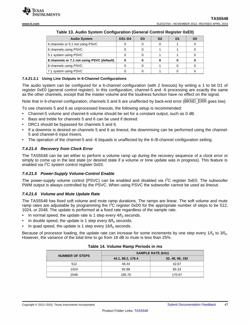
TAS5548www.ti.com SLES270A –NOVEMBER 2012–REVISED APRIL 2015
Table 13. Audio System Configuration (General Control Register 0xE0)Audio System D31–D4 D3 D2 D1 D0
6 channels or 5.1 not using PSVC 0 0 0 1 X6 channels using PSVC 0 0 1 1 X5.1 system using PSVC 0 0 1 1 X8 channels or 7.1 not using PSVC (default) 0 0 0 0 X8 channels using PSVC 0 0 1 0 X7.1 system using PSVC 0 0 1 0 X
7.4.21.3.1 Using Line Outputs in 6-Channel Configurations
The audio system can be configured for a 6-channel configuration (with 2 lineouts) by writing a 1 to bit D1 ofregister 0xE0 (general control register). In this configuration, channel-5 and -6 processing are exactly the sameas the other channels, except that the master volume and the loudness function have no effect on the signal.
Note that in 6-channel configuration, channels 5 and 6 are unaffected by back-end error (BKND_ERR goes low).
To use channels 5 and 6 as unprocessed lineouts, the following setup is recommended:• Channel-5 volume and channel-6 volume should be set for a constant output, such as 0 dB.• Bass and treble for channels 5 and 6 can be used if desired.• DRC1 should be bypassed for channels 5 and 6.• If a downmix is desired on channels 5 and 6 as lineout, the downmixing can be performed using the channel-
5 and channel-6 input mixers.• The operation of the channel-5 and -6 biquads is unaffected by the 6-/8-channel configuration setting.
7.4.21.4 Recovery from Clock ErrorThe TAS5548 can be set either to perform a volume ramp up during the recovery sequence of a clock error orsimply to come up in the last state (or desired state if a volume or tone update was in progress). This feature isenabled via I2C system control register 0x03.
7.4.21.5 Power-Supply Volume-Control EnableThe power-supply volume control (PSVC) can be enabled and disabled via I2C register 0xE0. The subwooferPWM output is always controlled by the PSVC. When using PSVC the subwoofer cannot be used as lineout.
7.4.21.6 Volume and Mute Update RateThe TAS5548 has fixed soft volume and mute ramp durations. The ramps are linear. The soft volume and muteramp rates are adjustable by programming the I2C register 0xD0 for the appropriate number of steps to be 512,1024, or 2048. The update is performed at a fixed rate regardless of the sample rate.• In normal speed, the update rate is 1 step every 4/fS seconds.• In double speed, the update is 1 step every 8/fS seconds.• In quad speed, the update is 1 step every 16/fS seconds.
Because of processor loading, the update rate can increase for some increments by one step every 1/fS to 3/fS.However, the variance of the total time to go from 18 dB to mute is less than 25%.
Table 14. Volume Ramp Periods in msSAMPLE RATE (kHz)
NUMBER OF STEPS44.1, 88.2, 176.4 32, 48, 96, 192
512 46.44 42.671024 92.88 85.332048 185.76 170.67
Copyright © 2012–2015, Texas Instruments Incorporated Submit Documentation Feedback 47
Product Folder Links: TAS5548
TAS5548SLES270A –NOVEMBER 2012–REVISED APRIL 2015 www.ti.com
7.4.21.7 Modulation Index LimitPWM modulation is a linear function of the audio signal. When the audio signal is 0, the PWM modulation is50%. When the audio signal increases toward full scale, the PWM modulation increases toward 100%. Fornegative signals, the PWM modulations fall below 50% toward 0%.
However, the maximum possible modulation does have a limit. During the off time period, the power stageconnected to the TAS5548 output needs to get ready for the next on-time period. The maximum possiblemodulation is then set by the power stage requirements. The default modulation index limit setting is 93.7%;however, some power stages may require a lower modulation limit. See the applicable power stage data sheetfor details on setting the modulation index limit. The default setting of 93.7% can be changed in the modulationindex register (0x16).
7.4.22 Master Clock and Serial Data Rate ControlsOn the TAS5548 the internal master clock is derived from the XTAL and the internal sampling rate will always be96 kHz (double speed mode) or 192 kHz (quad speed mode).
The TAS5548 can detect MCLK and the data rate automatically.
The MCLK frequency can be 64 fS, 128 fS, 196 fS, 256 fS, 384 fS, 512 fS, or 768 fS.
The TAS5548 accepts a 64 fS SCLK rate and a 1 fS LRCLK.
The clock and serial data interface have several control parameters:• MCLK ratio (64 fS, 128 fS, 196 fS, 256 fS, 384 fS, 512 fS, or 768 fS) – I2C parameter• Data rate (32, 44.1, 48, 88.2, 96, 176.4, 192 kHz) – I2C parameter• AM mode enable/disable – I2C parameter
7.4.22.1 192kHz Native Processing ModeThe TAS5548 ASRC defaults to 96kHz at startup. This means all DAP processing and filter calculations shouldbe based on 96kHz sample rate.
However, the TAS5548 is also capable of processing content at 192kHz (with a reduced channel count).
To enable 192kHz native mode• Write to 0xC5 ASRC Mode Control• Set D20 = 1 (Serial clock output sampling rate is the internal sampling rate)• Set D1:0 = 01 (192kHz Sampling Rate)• 0xC5 = 0011 0001
DAP processing and filter calculations should be based on 192kHz sample rate. This mode should be used withan incoming I2S rate of 192kHz
7.4.22.2 PLL OperationThe TAS5548 uses two internal clocks generated by two internal phase-locked loops (PLLs), the digital PLL(DPLL) and the analog PLL (APLL). The APLL provides the reference clock for the PWM. The DPLL provides thereference clock for the digital audio processor and the control logic.
The XTAL input provides the input reference clock for the APLL. The external crystal provides a time base tosupport a number of operations, including the detection of the MCLK ratio, the data rate, and clock errorconditions. The internal oscillator time base provides a constant rate for all controls and signal timing.
7.5 Programming
7.5.1 I2C Serial-Control Interface (Slave Addresses 0x36)The TAS5548 has a bidirectional I2C interface that is compatible with the Inter-IC (I2C) bus protocol and supportsboth 100-kbps and 400-kbps data transfer rates for single- and multiple-byte write and read operations. This is aslave-only device that does not support a multimaster bus environment or wait state insertion. The controlinterface is used to program the registers of the device and to read device status.
48 Submit Documentation Feedback Copyright © 2012–2015, Texas Instruments Incorporated
Product Folder Links: TAS5548
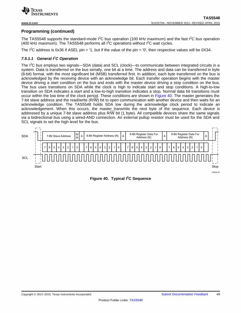
7-Bit Slave AddressR/W
8-Bit Register Address (N)A8-Bit Register Data For
Address (N)
Start Stop
SDA
SCL
7 6 5 4 3 2 1 0 7 6 5 4 3 2 1 0 7 6 5 4 3 2 1 0 7 6 5 4 3 2 1 0
A8-Bit Register Data For
Address (N)A A
T0035-01
TAS5548www.ti.com SLES270A –NOVEMBER 2012–REVISED APRIL 2015
Programming (continued)The TAS5548 supports the standard-mode I2C bus operation (100 kHz maximum) and the fast I2C bus operation(400 kHz maximum). The TAS5548 performs all I2C operations without I2C wait cycles.
The I2C address is 0x36 if ASEL pin = '1, but if the value of the pin = '0', then respective values will be 0X34.
7.5.1.1 General I2C OperationThe I2C bus employs two signals—SDA (data) and SCL (clock)—to communicate between integrated circuits in asystem. Data is transferred on the bus serially, one bit at a time. The address and data can be transferred in byte(8-bit) format, with the most significant bit (MSB) transferred first. In addition, each byte transferred on the bus isacknowledged by the receiving device with an acknowledge bit. Each transfer operation begins with the masterdevice driving a start condition on the bus and ends with the master device driving a stop condition on the bus.The bus uses transitions on SDA while the clock is high to indicate start and stop conditions. A high-to-lowtransition on SDA indicates a start and a low-to-high transition indicates a stop. Normal data bit transitions mustoccur within the low time of the clock period. These conditions are shown in Figure 40. The master generates the7-bit slave address and the read/write (R/W) bit to open communication with another device and then waits for anacknowledge condition. The TAS5548 holds SDA low during the acknowledge clock period to indicate anacknowledgement. When this occurs, the master transmits the next byte of the sequence. Each device isaddressed by a unique 7-bit slave address plus R/W bit (1 byte). All compatible devices share the same signalsvia a bidirectional bus using a wired-AND connection. An external pullup resistor must be used for the SDA andSCL signals to set the high level for the bus.
Figure 40. Typical I2C Sequence
Copyright © 2012–2015, Texas Instruments Incorporated Submit Documentation Feedback 49
Product Folder Links: TAS5548
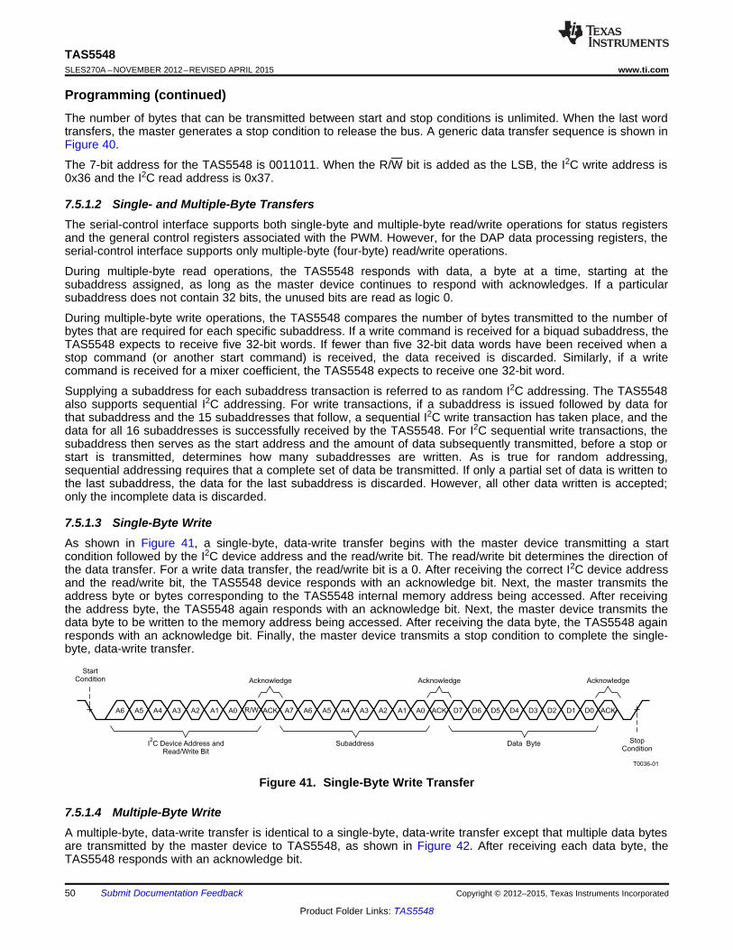
A6 A5 A4 A3 A2 A1 A0 R/W ACK A7 A6 A5 A4 A3 A2 A1 A0 ACK D7 D6 D5 D4 D3 D2 D1 D0 ACK
StartCondition
StopCondition
Acknowledge Acknowledge Acknowledge
I C Device Address and2
Read/Write BitSubaddress Data Byte
T0036-01
TAS5548SLES270A –NOVEMBER 2012–REVISED APRIL 2015 www.ti.com
Programming (continued)The number of bytes that can be transmitted between start and stop conditions is unlimited. When the last wordtransfers, the master generates a stop condition to release the bus. A generic data transfer sequence is shown inFigure 40.
The 7-bit address for the TAS5548 is 0011011. When the R/W bit is added as the LSB, the I2C write address is0x36 and the I2C read address is 0x37.
7.5.1.2 Single- and Multiple-Byte TransfersThe serial-control interface supports both single-byte and multiple-byte read/write operations for status registersand the general control registers associated with the PWM. However, for the DAP data processing registers, theserial-control interface supports only multiple-byte (four-byte) read/write operations.
During multiple-byte read operations, the TAS5548 responds with data, a byte at a time, starting at thesubaddress assigned, as long as the master device continues to respond with acknowledges. If a particularsubaddress does not contain 32 bits, the unused bits are read as logic 0.
During multiple-byte write operations, the TAS5548 compares the number of bytes transmitted to the number ofbytes that are required for each specific subaddress. If a write command is received for a biquad subaddress, theTAS5548 expects to receive five 32-bit words. If fewer than five 32-bit data words have been received when astop command (or another start command) is received, the data received is discarded. Similarly, if a writecommand is received for a mixer coefficient, the TAS5548 expects to receive one 32-bit word.
Supplying a subaddress for each subaddress transaction is referred to as random I2C addressing. The TAS5548also supports sequential I2C addressing. For write transactions, if a subaddress is issued followed by data forthat subaddress and the 15 subaddresses that follow, a sequential I2C write transaction has taken place, and thedata for all 16 subaddresses is successfully received by the TAS5548. For I2C sequential write transactions, thesubaddress then serves as the start address and the amount of data subsequently transmitted, before a stop orstart is transmitted, determines how many subaddresses are written. As is true for random addressing,sequential addressing requires that a complete set of data be transmitted. If only a partial set of data is written tothe last subaddress, the data for the last subaddress is discarded. However, all other data written is accepted;only the incomplete data is discarded.
7.5.1.3 Single-Byte WriteAs shown in Figure 41, a single-byte, data-write transfer begins with the master device transmitting a startcondition followed by the I2C device address and the read/write bit. The read/write bit determines the direction ofthe data transfer. For a write data transfer, the read/write bit is a 0. After receiving the correct I2C device addressand the read/write bit, the TAS5548 device responds with an acknowledge bit. Next, the master transmits theaddress byte or bytes corresponding to the TAS5548 internal memory address being accessed. After receivingthe address byte, the TAS5548 again responds with an acknowledge bit. Next, the master device transmits thedata byte to be written to the memory address being accessed. After receiving the data byte, the TAS5548 againresponds with an acknowledge bit. Finally, the master device transmits a stop condition to complete the single-byte, data-write transfer.
Figure 41. Single-Byte Write Transfer
7.5.1.4 Multiple-Byte WriteA multiple-byte, data-write transfer is identical to a single-byte, data-write transfer except that multiple data bytesare transmitted by the master device to TAS5548, as shown in Figure 42. After receiving each data byte, theTAS5548 responds with an acknowledge bit.
50 Submit Documentation Feedback Copyright © 2012–2015, Texas Instruments Incorporated
Product Folder Links: TAS5548
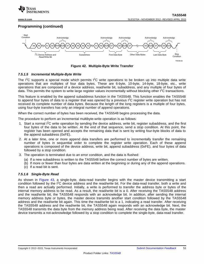
D7 D0 ACK
StopCondition
Acknowledge
I C Device Address and2
Read/Write BitSubaddress Last Data Byte
A6 A5 A1 A0 R/W ACK A7 A5 A1 A0 ACK D7 ACK
StartCondition Acknowledge Acknowledge Acknowledge
First Data Byte
A4 A3A6
Other Data Bytes
ACK
Acknowledge
D0 D7 D0
T0036-02
TAS5548www.ti.com SLES270A –NOVEMBER 2012–REVISED APRIL 2015
Programming (continued)
Figure 42. Multiple-Byte Write Transfer
7.5.1.5 Incremental Multiple-Byte WriteThe I2C supports a special mode which permits I2C write operations to be broken up into multiple data writeoperations that are multiples of four data bytes. These are 6-byte, 10-byte, 14-byte, 18-byte, etc., writeoperations that are composed of a device address, read/write bit, subaddress, and any multiple of four bytes ofdata. This permits the system to write large register values incrementally without blocking other I2C transactions.
This feature is enabled by the append subaddress function in the TAS5548. This function enables the TAS5548to append four bytes of data to a register that was opened by a previous I2C register write operation but has notreceived its complete number of data bytes. Because the length of the long registers is a multiple of four bytes,using four-byte transfers has only an integral number of append operations.
When the correct number of bytes has been received, the TAS5548 begins processing the data.
The procedure to perform an incremental multibyte-write operation is as follows:1. Start a normal I2C write operation by sending the device address, write bit, register subaddress, and the first
four bytes of the data to be written. At the end of that sequence, send a stop condition. At this point, theregister has been opened and accepts the remaining data that is sent by writing four-byte blocks of data tothe append subaddress (0xFE).
2. At a later time, one or more append data transfers are performed to incrementally transfer the remainingnumber of bytes in sequential order to complete the register write operation. Each of these appendoperations is composed of the device address, write bit, append subaddress (0xFE), and four bytes of datafollowed by a stop condition.
3. The operation is terminated due to an error condition, and the data is flushed:(a) If a new subaddress is written to the TAS5548 before the correct number of bytes are written.(b) If more or fewer than four bytes are data written at the beginning or during any of the append operations.(c) If a read bit is sent.
7.5.1.6 Single-Byte ReadAs shown in Figure 43, a single-byte, data-read transfer begins with the master device transmitting a startcondition followed by the I2C device address and the read/write bit. For the data-read transfer, both a write andthen a read are actually performed. Initially, a write is performed to transfer the address byte or bytes of theinternal memory address to be read. As a result, the read/write bit is a 0. After receiving the TAS5548 addressand the read/write bit, the TAS5548 responds with an acknowledge bit. In addition, after sending the internalmemory address byte or bytes, the master device transmits another start condition followed by the TAS5548address and the read/write bit again. This time the read/write bit is a 1, indicating a read transfer. After receivingthe TAS5548 address and the read/write bit, the TAS5548 again responds with an acknowledge bit. Next, theTAS5548 transmits the data byte from the memory address being read. After receiving the data byte, the masterdevice transmits a not-acknowledge followed by a stop condition to complete the single-byte, data-read transfer.
Copyright © 2012–2015, Texas Instruments Incorporated Submit Documentation Feedback 51
Product Folder Links: TAS5548
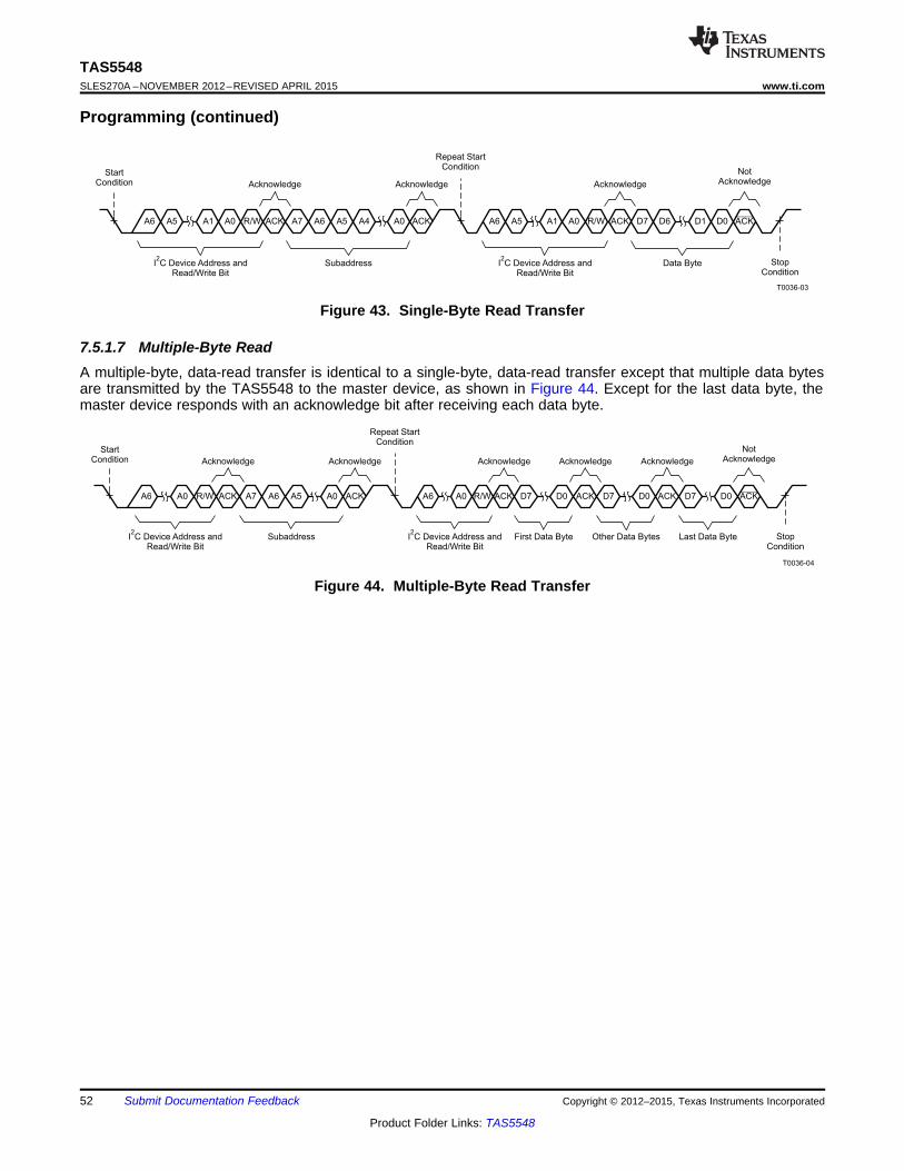
A6 A0 ACK
Acknowledge
I C Device Address andRead/Write Bit
2
R/WA6 A0 R/W ACK A0 ACK D7 D0 ACK
StartCondition
StopCondition
Acknowledge Acknowledge Acknowledge
Last Data Byte
ACK
First Data Byte
Repeat StartCondition
NotAcknowledge
I C Device Address andRead/Write Bit
2Subaddress Other Data Bytes
A7 A6 A5 D7 D0 ACK
Acknowledge
D7 D0
T0036-04
A6 A5 A0 R/W ACK A7 A6 A5 A4 A0 ACK A6 A5 A0 ACK
StartCondition
StopCondition
Acknowledge Acknowledge Acknowledge
I C Device Address and2
Read/Write BitSubaddress Data Byte
D7 D6 D1 D0 ACK
I C Device Address andRead/Write Bit
2
NotAcknowledge
R/WA1 A1
Repeat StartCondition
T0036-03
TAS5548SLES270A –NOVEMBER 2012–REVISED APRIL 2015 www.ti.com
Programming (continued)
Figure 43. Single-Byte Read Transfer
7.5.1.7 Multiple-Byte ReadA multiple-byte, data-read transfer is identical to a single-byte, data-read transfer except that multiple data bytesare transmitted by the TAS5548 to the master device, as shown in Figure 44. Except for the last data byte, themaster device responds with an acknowledge bit after receiving each data byte.
Figure 44. Multiple-Byte Read Transfer
52 Submit Documentation Feedback Copyright © 2012–2015, Texas Instruments Incorporated
Product Folder Links: TAS5548
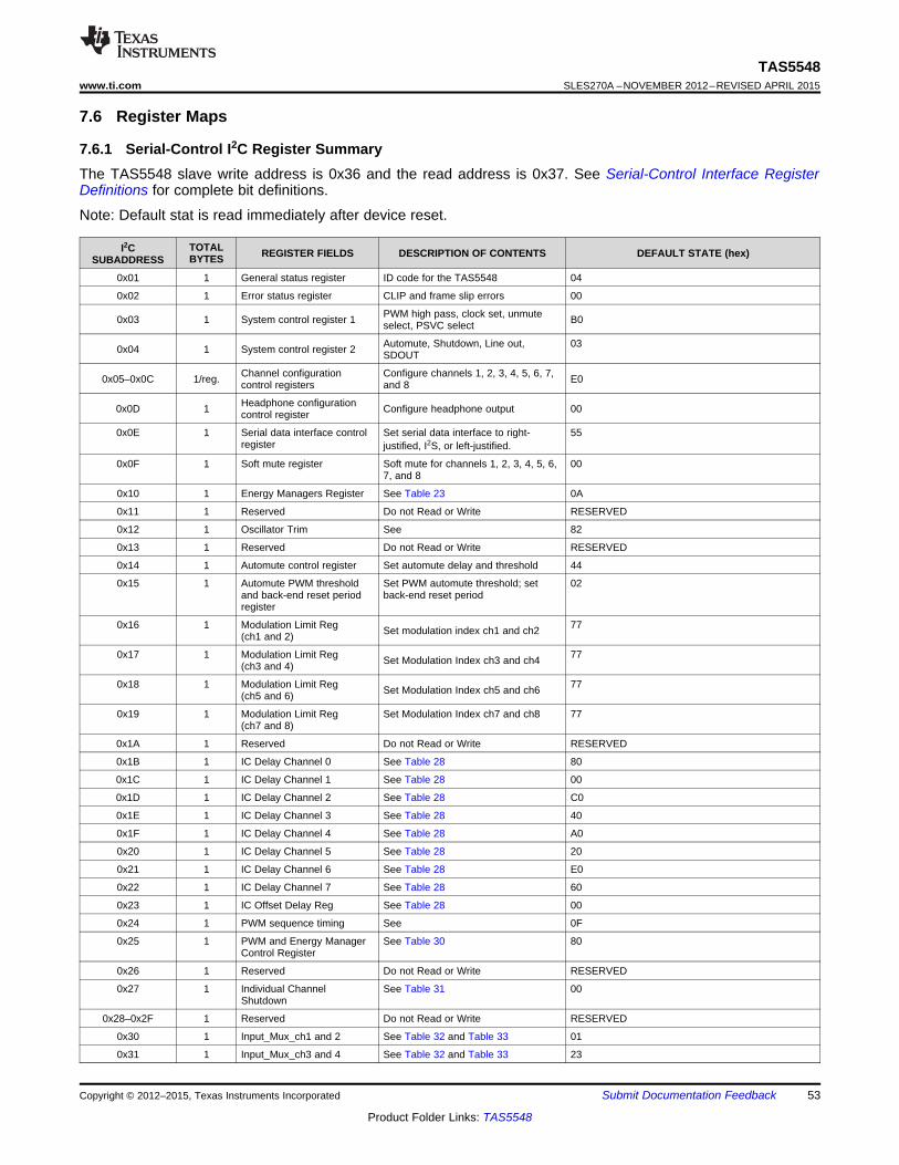
TAS5548www.ti.com SLES270A –NOVEMBER 2012–REVISED APRIL 2015
7.6 Register Maps
7.6.1 Serial-Control I2C Register SummaryThe TAS5548 slave write address is 0x36 and the read address is 0x37. See Serial-Control Interface RegisterDefinitions for complete bit definitions.
Note: Default stat is read immediately after device reset.
TOTALI2C REGISTER FIELDS DESCRIPTION OF CONTENTS DEFAULT STATE (hex)BYTESSUBADDRESS
0x01 1 General status register ID code for the TAS5548 04
0x02 1 Error status register CLIP and frame slip errors 00
PWM high pass, clock set, unmute0x03 1 System control register 1 B0select, PSVC select
Automute, Shutdown, Line out, 030x04 1 System control register 2 SDOUT
Channel configuration Configure channels 1, 2, 3, 4, 5, 6, 7,0x05–0x0C 1/reg. E0control registers and 8
Headphone configuration0x0D 1 Configure headphone output 00control register
0x0E 1 Serial data interface control Set serial data interface to right- 55register justified, I2S, or left-justified.
0x0F 1 Soft mute register Soft mute for channels 1, 2, 3, 4, 5, 6, 007, and 8
0x10 1 Energy Managers Register See Table 23 0A
0x11 1 Reserved Do not Read or Write RESERVED
0x12 1 Oscillator Trim See 82
0x13 1 Reserved Do not Read or Write RESERVED
0x14 1 Automute control register Set automute delay and threshold 44
0x15 1 Automute PWM threshold Set PWM automute threshold; set 02and back-end reset period back-end reset periodregister
0x16 1 Modulation Limit Reg 77Set modulation index ch1 and ch2(ch1 and 2)
0x17 1 Modulation Limit Reg 77Set Modulation Index ch3 and ch4(ch3 and 4)
0x18 1 Modulation Limit Reg 77Set Modulation Index ch5 and ch6(ch5 and 6)
0x19 1 Modulation Limit Reg Set Modulation Index ch7 and ch8 77(ch7 and 8)
0x1A 1 Reserved Do not Read or Write RESERVED
0x1B 1 IC Delay Channel 0 See Table 28 80
0x1C 1 IC Delay Channel 1 See Table 28 00
0x1D 1 IC Delay Channel 2 See Table 28 C0
0x1E 1 IC Delay Channel 3 See Table 28 40
0x1F 1 IC Delay Channel 4 See Table 28 A0
0x20 1 IC Delay Channel 5 See Table 28 20
0x21 1 IC Delay Channel 6 See Table 28 E0
0x22 1 IC Delay Channel 7 See Table 28 60
0x23 1 IC Offset Delay Reg See Table 28 00
0x24 1 PWM sequence timing See 0F
0x25 1 PWM and Energy Manager See Table 30 80Control Register
0x26 1 Reserved Do not Read or Write RESERVED
0x27 1 Individual Channel See Table 31 00Shutdown
0x28–0x2F 1 Reserved Do not Read or Write RESERVED
0x30 1 Input_Mux_ch1 and 2 See Table 32 and Table 33 01
0x31 1 Input_Mux_ch3 and 4 See Table 32 and Table 33 23
Copyright © 2012–2015, Texas Instruments Incorporated Submit Documentation Feedback 53
Product Folder Links: TAS5548
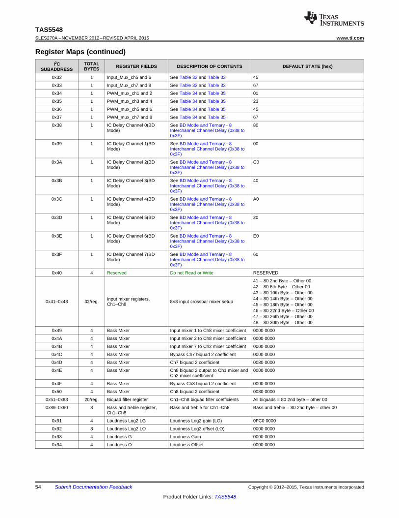
TAS5548SLES270A –NOVEMBER 2012–REVISED APRIL 2015 www.ti.com
Register Maps (continued)TOTALI2C REGISTER FIELDS DESCRIPTION OF CONTENTS DEFAULT STATE (hex)BYTESSUBADDRESS
0x32 1 Input_Mux_ch5 and 6 See Table 32 and Table 33 45
0x33 1 Input_Mux_ch7 and 8 See Table 32 and Table 33 67
0x34 1 PWM_mux_ch1 and 2 See Table 34 and Table 35 01
0x35 1 PWM_mux_ch3 and 4 See Table 34 and Table 35 23
0x36 1 PWM_mux_ch5 and 6 See Table 34 and Table 35 45
0x37 1 PWM_mux_ch7 and 8 See Table 34 and Table 35 67
0x38 1 IC Delay Channel 0(BD See BD Mode and Ternary - 8 80Mode) Interchannel Channel Delay (0x38 to
0x3F)
0x39 1 IC Delay Channel 1(BD See BD Mode and Ternary - 8 00Mode) Interchannel Channel Delay (0x38 to
0x3F)
0x3A 1 IC Delay Channel 2(BD See BD Mode and Ternary - 8 C0Mode) Interchannel Channel Delay (0x38 to
0x3F)
0x3B 1 IC Delay Channel 3(BD See BD Mode and Ternary - 8 40Mode) Interchannel Channel Delay (0x38 to
0x3F)
0x3C 1 IC Delay Channel 4(BD See BD Mode and Ternary - 8 A0Mode) Interchannel Channel Delay (0x38 to
0x3F)
0x3D 1 IC Delay Channel 5(BD See BD Mode and Ternary - 8 20Mode) Interchannel Channel Delay (0x38 to
0x3F)
0x3E 1 IC Delay Channel 6(BD See BD Mode and Ternary - 8 E0Mode) Interchannel Channel Delay (0x38 to
0x3F)
0x3F 1 IC Delay Channel 7(BD See BD Mode and Ternary - 8 60Mode) Interchannel Channel Delay (0x38 to
0x3F)
0x40 4 Reserved Do not Read or Write RESERVED
41 – 80 2nd Byte – Other 0042 – 80 6th Byte – Other 0043 – 80 10th Byte – Other 0044 – 80 14th Byte – Other 00Input mixer registers,0x41–0x48 32/reg. 8×8 input crossbar mixer setupCh1–Ch8 45 – 80 18th Byte – Other 0046 – 80 22nd Byte – Other 0047 – 80 26th Byte – Other 0048 – 80 30th Byte – Other 00
0x49 4 Bass Mixer Input mixer 1 to Ch8 mixer coefficient 0000 0000
0x4A 4 Bass Mixer Input mixer 2 to Ch8 mixer coefficient 0000 0000
0x4B 4 Bass Mixer Input mixer 7 to Ch2 mixer coefficient 0000 0000
0x4C 4 Bass Mixer Bypass Ch7 biquad 2 coefficient 0000 0000
0x4D 4 Bass Mixer Ch7 biquad 2 coefficient 0080 0000
0x4E 4 Bass Mixer Ch8 biquad 2 output to Ch1 mixer and 0000 0000Ch2 mixer coefficient
0x4F 4 Bass Mixer Bypass Ch8 biquad 2 coefficient 0000 0000
0x50 4 Bass Mixer Ch8 biquad 2 coefficient 0080 0000
0x51–0x88 20/reg. Biquad filter register Ch1–Ch8 biquad filter coefficients All biquads = 80 2nd byte – other 00
0x89–0x90 8 Bass and treble register, Bass and treble for Ch1–Ch8 Bass and treble = 80 2nd byte – other 00Ch1–Ch8
0x91 4 Loudness Log2 LG Loudness Log2 gain (LG) 0FC0 0000
0x92 8 Loudness Log2 LO Loudness Log2 offset (LO) 0000 0000
0x93 4 Loudness G Loudness Gain 0000 0000
0x94 4 Loudness O Loudness Offset 0000 0000
54 Submit Documentation Feedback Copyright © 2012–2015, Texas Instruments Incorporated
Product Folder Links: TAS5548
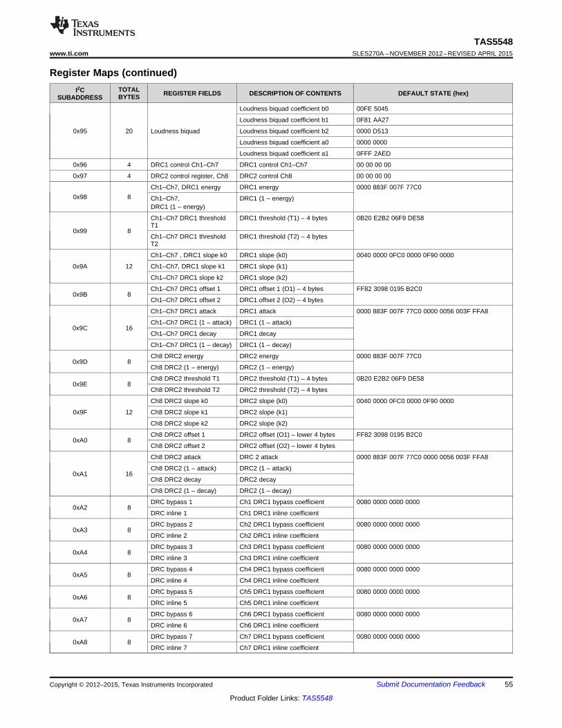
TAS5548www.ti.com SLES270A –NOVEMBER 2012–REVISED APRIL 2015
Register Maps (continued)TOTALI2C REGISTER FIELDS DESCRIPTION OF CONTENTS DEFAULT STATE (hex)BYTESSUBADDRESS
Loudness biquad coefficient b0 00FE 5045
Loudness biquad coefficient b1 0F81 AA27
0x95 20 Loudness biquad Loudness biquad coefficient b2 0000 D513
Loudness biquad coefficient a0 0000 0000
Loudness biquad coefficient a1 0FFF 2AED
0x96 4 DRC1 control Ch1–Ch7 DRC1 control Ch1–Ch7 00 00 00 00
0x97 4 DRC2 control register, Ch8 DRC2 control Ch8 00 00 00 00
Ch1–Ch7, DRC1 energy DRC1 energy 0000 883F 007F 77C00x98 8 Ch1–Ch7, DRC1 (1 – energy)
DRC1 (1 – energy)
Ch1–Ch7 DRC1 threshold DRC1 threshold (T1) – 4 bytes 0B20 E2B2 06F9 DE58T1
0x99 8Ch1–Ch7 DRC1 threshold DRC1 threshold (T2) – 4 bytesT2
Ch1–Ch7 , DRC1 slope k0 DRC1 slope (k0) 0040 0000 0FC0 0000 0F90 0000
0x9A 12 Ch1–Ch7, DRC1 slope k1 DRC1 slope (k1)
Ch1–Ch7 DRC1 slope k2 DRC1 slope (k2)
Ch1–Ch7 DRC1 offset 1 DRC1 offset 1 (O1) – 4 bytes FF82 3098 0195 B2C00x9B 8
Ch1–Ch7 DRC1 offset 2 DRC1 offset 2 (O2) – 4 bytes
Ch1–Ch7 DRC1 attack DRC1 attack 0000 883F 007F 77C0 0000 0056 003F FFA8
Ch1–Ch7 DRC1 (1 – attack) DRC1 (1 – attack)0x9C 16
Ch1–Ch7 DRC1 decay DRC1 decay
Ch1–Ch7 DRC1 (1 – decay) DRC1 (1 – decay)
Ch8 DRC2 energy DRC2 energy 0000 883F 007F 77C00x9D 8
Ch8 DRC2 (1 – energy) DRC2 (1 – energy)
Ch8 DRC2 threshold T1 DRC2 threshold (T1) – 4 bytes 0B20 E2B2 06F9 DE580x9E 8
Ch8 DRC2 threshold T2 DRC2 threshold (T2) – 4 bytes
Ch8 DRC2 slope k0 DRC2 slope (k0) 0040 0000 0FC0 0000 0F90 0000
0x9F 12 Ch8 DRC2 slope k1 DRC2 slope (k1)
Ch8 DRC2 slope k2 DRC2 slope (k2)
Ch8 DRC2 offset 1 DRC2 offset (O1) – lower 4 bytes FF82 3098 0195 B2C00xA0 8
Ch8 DRC2 offset 2 DRC2 offset (O2) – lower 4 bytes
Ch8 DRC2 attack DRC 2 attack 0000 883F 007F 77C0 0000 0056 003F FFA8
Ch8 DRC2 (1 – attack) DRC2 (1 – attack)0xA1 16
Ch8 DRC2 decay DRC2 decay
Ch8 DRC2 (1 – decay) DRC2 (1 – decay)
DRC bypass 1 Ch1 DRC1 bypass coefficient 0080 0000 0000 00000xA2 8
DRC inline 1 Ch1 DRC1 inline coefficient
DRC bypass 2 Ch2 DRC1 bypass coefficient 0080 0000 0000 00000xA3 8
DRC inline 2 Ch2 DRC1 inline coefficient
DRC bypass 3 Ch3 DRC1 bypass coefficient 0080 0000 0000 00000xA4 8
DRC inline 3 Ch3 DRC1 inline coefficient
DRC bypass 4 Ch4 DRC1 bypass coefficient 0080 0000 0000 00000xA5 8
DRC inline 4 Ch4 DRC1 inline coefficient
DRC bypass 5 Ch5 DRC1 bypass coefficient 0080 0000 0000 00000xA6 8
DRC inline 5 Ch5 DRC1 inline coefficient
DRC bypass 6 Ch6 DRC1 bypass coefficient 0080 0000 0000 00000xA7 8
DRC inline 6 Ch6 DRC1 inline coefficient
DRC bypass 7 Ch7 DRC1 bypass coefficient 0080 0000 0000 00000xA8 8
DRC inline 7 Ch7 DRC1 inline coefficient
Copyright © 2012–2015, Texas Instruments Incorporated Submit Documentation Feedback 55
Product Folder Links: TAS5548
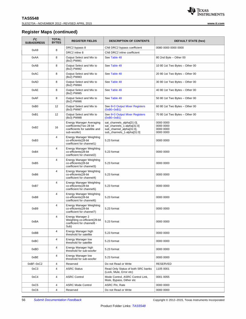
TAS5548SLES270A –NOVEMBER 2012–REVISED APRIL 2015 www.ti.com
Register Maps (continued)TOTALI2C REGISTER FIELDS DESCRIPTION OF CONTENTS DEFAULT STATE (hex)BYTESSUBADDRESS
DRC2 bypass 8 Ch8 DRC2 bypass coefficient 0080 0000 0000 00000xA9 8
DRC2 inline 8 Ch8 DRC2 inline coefficient
0xAA 8 Output Select and Mix to See Table 48 80 2nd Byte – Other 00(8x2) PWM1
0xAB 8 Output Select and Mix to See Table 48 10 80 1st Two Bytes – Other 00(8x2) PWM2
0xAC 8 Output Select and Mix to See Table 48 20 80 1st Two Bytes – Other 00(8x2) PWM3
0xAD 8 Output Select and Mix to See Table 48 30 80 1st Two Bytes – Other 00(8x2) PWM4
0xAE 8 Output Select and Mix to See Table 48 40 80 1st Two Bytes – Other 00(8x2) PWM5
0xAF 8 Output Select and Mix to See Table 48 50 80 1st Two Bytes – Other 00(8x2) PWM6
0xB0 12 Output Select and Mix to See 8×3 Output Mixer Registers 60 80 1st Two Bytes – Other 00(8x3) PWM7 (0xB0–0xB1)
0xB1 12 Output Select and Mix to See 8×3 Output Mixer Registers 70 80 1st Two Bytes – Other 00(8x3) PWM8 (0xB0–0xB1)
Energy Manager Averaging sat_channels_alpha[31:0], 0000 0000coefficients(Two 28 bit sat_channels_1-alpha[31:0] 0000 00000xB2 16 coefficients for satellite and sub_channel_alpha[31:0], 0000 0000sub-woofer) sub_channels_1-alpha[31:0] 0000 0000
4 Energy Manager Weighting0xB3 co-efficients(28-bit 5.23 format 0000 0000
coefficient for channel1)
4 Energy Manager Weighting0xB4 co-efficients(28-bit 5.23 format 0000 0000
coefficient for channel2)
4 Energy Manager Weighting0xB5 co-efficients(28-bit 5.23 format 0000 0000
coefficient for channel3)
4 Energy Manager Weighting0xB6 co-efficients(28-bit 5.23 format 0000 0000
coefficient for channel4)
4 Energy Manager Weighting0xB7 co-efficients(28-bit 5.23 format 0000 0000
coefficient for channel5)
4 Energy Manager Weighting0xB8 co-efficients(28-bit 5.23 format 0000 0000
coefficient for channel6)
4 Energy Manager Weighting0xB9 co-efficients(28-bit 5.23 format 0000 0000
coefficient for channel7)
4 Energy Manager 2Weighting co-efficient(28-bit0xBA 5.23 format 0000 0000coefficient for channel8 -Sub)
4 Energy Manager high0xBB 5.23 format 0000 0000threshold for satellite
4 Energy Manager low0xBC 5.23 format 0000 0000threshold for satellite
4 Energy Manager high0xBD 5.23 format 0000 0000threshold for sub-woofer
4 Energy Manager low0xBE 5.23 format 0000 0000threshold for sub-woofer
0xBF–0xC2 4 Reserved Do not Read or Write RESERVED
0xC3 4 ASRC Status Read Only Status of both SRC banks 1105 0001(Lock, Mute, Error etc)
0xC4 4 ASRC Control Mode Control, ASRC Control Link, 0001 0055Mute, Bypass, Dither etc
0xC5 4 ASRC Mode Control ASRC Pin, Rate 0000 0000
0xC6 4 Reserved Do not Read or Write 0000 0000
56 Submit Documentation Feedback Copyright © 2012–2015, Texas Instruments Incorporated
Product Folder Links: TAS5548
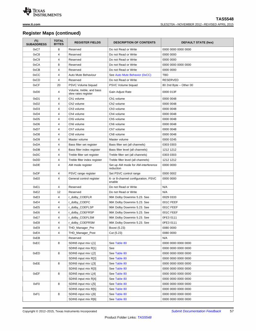
TAS5548www.ti.com SLES270A –NOVEMBER 2012–REVISED APRIL 2015
Register Maps (continued)TOTALI2C REGISTER FIELDS DESCRIPTION OF CONTENTS DEFAULT STATE (hex)BYTESSUBADDRESS
0xC7 8 Reserved Do not Read or Write 0000 0000 0000 0000
0xC8 4 Reserved Do not Read or Write 0000 0000
0xC9 4 Reserved Do not Read or Write 0000 0000
0xCA 8 Reserved Do not Read or Write 0000 0000 0000 0000
0xCB 4 Reserved Do not Read or Write 0000 0000
0xCC 4 Auto Mute Behaviour See Auto Mute Behavior (0xCC) TBD
0xCD 4 Reserved Do not Read or Write RESERVED
0xCF 20 PSVC Volume biquad PSVC Volume biquad 80 2nd Byte – Other 00
Volume, treble, and bass0xD0 4 Gain Adjust Rate 0000 013Fslew rates register
0xD1 4 Ch1 volume Ch1 volume 0000 0048
0xD2 4 Ch2 volume Ch2 volume 0000 0048
0xD3 4 Ch3 volume Ch3 volume 0000 0048
0xD4 4 Ch4 volume Ch4 volume 0000 0048
0xD5 4 Ch5 volume Ch5 volume 0000 0048
0xD6 4 Ch6 volume Ch6 volume 0000 0048
0xD7 4 Ch7 volume Ch7 volume 0000 0048
0xD8 4 Ch8 volume Ch8 volume 0000 0048
0xD9 4 Master volume Master volume 0000 0245
0xDA 4 Bass filter set register Bass filter set (all channels) 0303 0303
0xDB 4 Bass filter index register Bass filter level (all channels) 1212 1212
0xDC 4 Treble filter set register Treble filter set (all channels) 0303 0303
0xDD 4 Treble filter index register Treble filter level (all channels) 1212 1212
0xDE 4 AM mode register Set up AM mode for AM-interference 0000 0000reduction
0xDF 4 PSVC range register Set PSVC control range 0000 0002
0xE0 4 General control register 6- or 8-channel configuration, PSVC 0000 0000enable
0xE1 4 Reserved Do not Read or Write N/A
0xE2 12 Reserved Do not Read or Write N/A
0xE3 4 r_dolby_COEFLR 96K Dolby Downmix 5.23. See 0029 0333
0xE4 4 r_dolby_COEFC 96K Dolby Downmix 5.23. See 001C FEEF
0xE5 4 r_dolby_COEFLSP 96K Dolby Downmix 5.23. See 001C FEEF
0xE6 4 r_dolby_COEFRSP 96K Dolby Downmix 5.23. See 001C FEEF
0xE7 4 r_dolby_COEFLSM 96K Dolby Downmix 5.23. See 0FE3 0111
0xE8 4 r_dolby_COEFRSM 96K Dolby Downmix 5.23. See 0FE3 0111
0xE9 4 THD_Manager_Pre Boost (5.23) 0080 0000
0xEA 4 THD_Manager_Post Cut (5.23) 0080 0000
0xEB Reserved N/A
0xEC 8 SDIN5 input mix L[1] See Table 80 0000 0000 0000 0000
SDIN5 input mix R[1] See 0000 0000 0000 0000
0xED 8 SDIN5 input mix L[2] See Table 80 0000 0000 0000 0000
SDIN5 input mix R[2] See Table 80 0000 0000 0000 0000
0xEE 8 SDIN5 input mix L[3] See Table 80 0000 0000 0000 0000
SDIN5 input mix R[3] See Table 80 0000 0000 0000 0000
0xEF 8 SDIN5 input mix L[4] See Table 80 0000 0000 0000 0000
SDIN5 input mix R[4] See Table 80 0000 0000 0000 0000
0xF0 8 SDIN5 input mix L[5] See Table 80 0000 0000 0000 0000
SDIN5 input mix R[5] See Table 80 0000 0000 0000 0000
0xF1 8 SDIN5 input mix L[6] See Table 80 0000 0000 0000 0000
SDIN5 input mix R[6] See Table 80 0000 0000 0000 0000
Copyright © 2012–2015, Texas Instruments Incorporated Submit Documentation Feedback 57
Product Folder Links: TAS5548
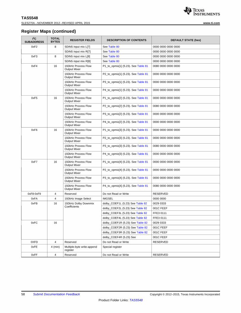
TAS5548SLES270A –NOVEMBER 2012–REVISED APRIL 2015 www.ti.com
Register Maps (continued)TOTALI2C REGISTER FIELDS DESCRIPTION OF CONTENTS DEFAULT STATE (hex)BYTESSUBADDRESS
0xF2 8 SDIN5 input mix L[7] See Table 80 0000 0000 0000 0000
SDIN5 input mix R[7] See Table 80 0000 0000 0000 0000
0xF3 8 SDIN5 input mix L[8] See Table 80 0000 0000 0000 0000
SDIN5 input mix R[8] See Table 80 0000 0000 0000 0000
0xF4 16 192kHz Process Flow P1_to_opmix[1] (5.23). See Table 81 0080 0000 0000 0000Output Mixer
192kHz Process Flow P2_to_opmix[1] (5.23). See Table 81 0000 0000 0000 0000Output Mixer
192kHz Process Flow P3_to_opmix[1] (5.23). See Table 81 0000 0000 0000 0000Output Mixer
192kHz Process Flow P4_to_opmix[1] (5.23). See Table 81 0000 0000 0000 0000Output Mixer
0xF5 16 192kHz Process Flow P1_to_opmix[2] (5.23). See Table 81 0000 0000 0000 0000Output Mixer
192kHz Process Flow P2_to_opmix[2] (5.23). See Table 81 0080 0000 0000 0000Output Mixer
192kHz Process Flow P3_to_opmix[2] (5.23). See Table 81 0000 0000 0000 0000Output Mixer
192kHz Process Flow P4_to_opmix[2] (5.23). See Table 81 0000 0000 0000 0000Output Mixer
0xF6 16 192kHz Process Flow P1_to_opmix[3] (5.23). See Table 81 0000 0000 0000 0000Output Mixer
192kHz Process Flow P2_to_opmix[3] (5.23). See Table 81 0000 0000 0000 0000Output Mixer
192kHz Process Flow P3_to_opmix[3] (5.23). See Table 81 0080 0000 0000 0000Output Mixer
192kHz Process Flow P4_to_opmix[3] (5.23). See Table 81 0000 0000 0000 0000Output Mixer
0xF7 16 192kHz Process Flow P1_to_opmix[4] (5.23). See Table 81 0000 0000 0000 0000Output Mixer
192kHz Process Flow P2_to_opmix[4] (5.23). See Table 81 0000 0000 0000 0000Output Mixer
192kHz Process Flow P3_to_opmix[4] (5.23). See Table 81 0000 0000 0000 0000Output Mixer
192kHz Process Flow P4_to_opmix[4] (5.23). See Table 81 0080 0000 0000 0000Output Mixer
0xF8-0xF9 4 Reserved Do not Read or Write RESERVED
0xFA 4 192kHz Image Select IMGSEL 0000 0000
0xFB 16 192kHz Dolby Downmix dolby_COEF1L (5.23) See Table 82 0029 0333Coefficients dolby_COEF2L (5.23) See Table 82 001C FEEF
dolby_COEF3L (5.23) See Table 82 FFE3 0111
dolby_COEF4L (5.23) See Table 82 FFE3 0111
0xFC 16 dolby_COEF1R (5.23) See Table 82 0029 0333
dolby_COEF2R (5.23) See Table 82 001C FEEF
dolby_COEF3R (5.23) See Table 82 001C FEEF
dolby_COEF4R (5.23) See 001C FEEF
0XFD 4 Reserved Do not Read or Write RESERVED
0xFE 4 (min) Multiple-byte write-append Special registerregister
0xFF 4 Reserved Do not Read or Write RESERVED
58 Submit Documentation Feedback Copyright © 2012–2015, Texas Instruments Incorporated
Product Folder Links: TAS5548
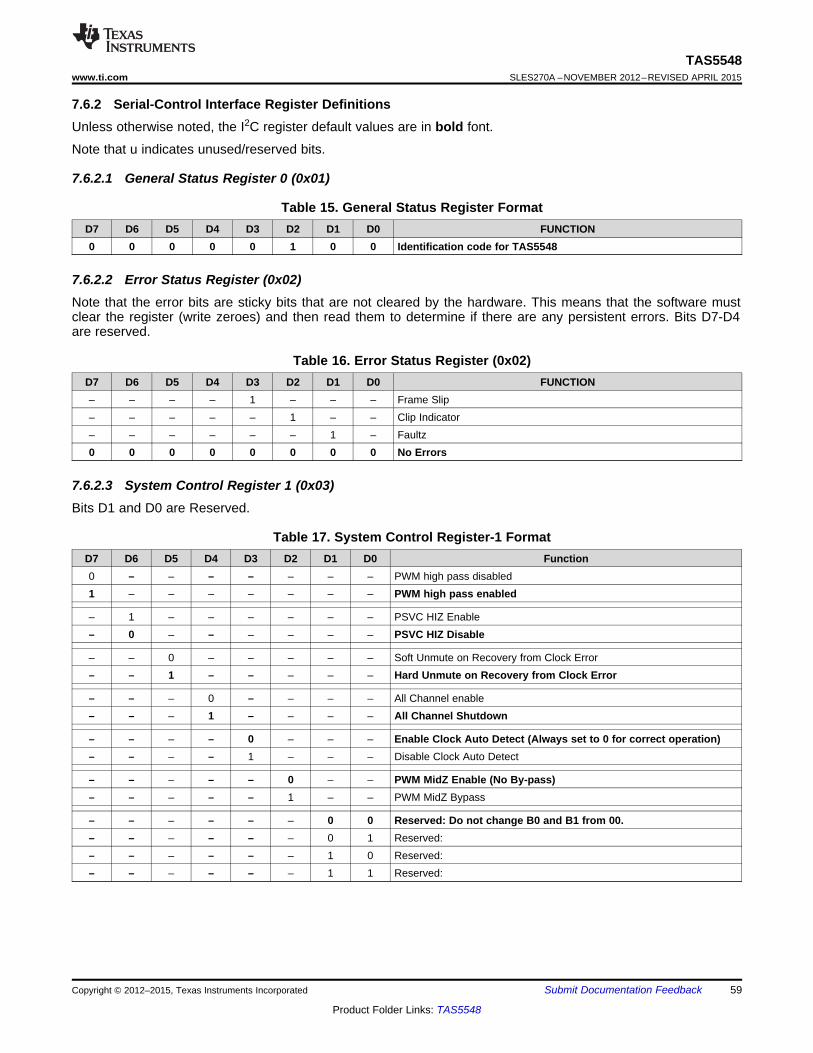
TAS5548www.ti.com SLES270A –NOVEMBER 2012–REVISED APRIL 2015
7.6.2 Serial-Control Interface Register DefinitionsUnless otherwise noted, the I2C register default values are in bold font.
Note that u indicates unused/reserved bits.
7.6.2.1 General Status Register 0 (0x01)
Table 15. General Status Register FormatD7 D6 D5 D4 D3 D2 D1 D0 FUNCTION0 0 0 0 0 1 0 0 Identification code for TAS5548
7.6.2.2 Error Status Register (0x02)Note that the error bits are sticky bits that are not cleared by the hardware. This means that the software mustclear the register (write zeroes) and then read them to determine if there are any persistent errors. Bits D7-D4are reserved.
Table 16. Error Status Register (0x02)D7 D6 D5 D4 D3 D2 D1 D0 FUNCTION– – – – 1 – – – Frame Slip– – – – – 1 – – Clip Indicator– – – – – – 1 – Faultz0 0 0 0 0 0 0 0 No Errors
7.6.2.3 System Control Register 1 (0x03)Bits D1 and D0 are Reserved.
Table 17. System Control Register-1 FormatD7 D6 D5 D4 D3 D2 D1 D0 Function0 – – – – – – – PWM high pass disabled1 – – – – – – – PWM high pass enabled
– 1 – – – – – – PSVC HIZ Enable– 0 – – – – – – PSVC HIZ Disable
– – 0 – – – – – Soft Unmute on Recovery from Clock Error– – 1 – – – – – Hard Unmute on Recovery from Clock Error
– – – 0 – – – – All Channel enable– – – 1 – – – – All Channel Shutdown
– – – – 0 – – – Enable Clock Auto Detect (Always set to 0 for correct operation)– – – – 1 – – – Disable Clock Auto Detect
– – – – – 0 – – PWM MidZ Enable (No By-pass)– – – – – 1 – – PWM MidZ Bypass
– – – – – – 0 0 Reserved: Do not change B0 and B1 from 00.– – – – – – 0 1 Reserved:– – – – – – 1 0 Reserved:– – – – – – 1 1 Reserved:
Copyright © 2012–2015, Texas Instruments Incorporated Submit Documentation Feedback 59
Product Folder Links: TAS5548
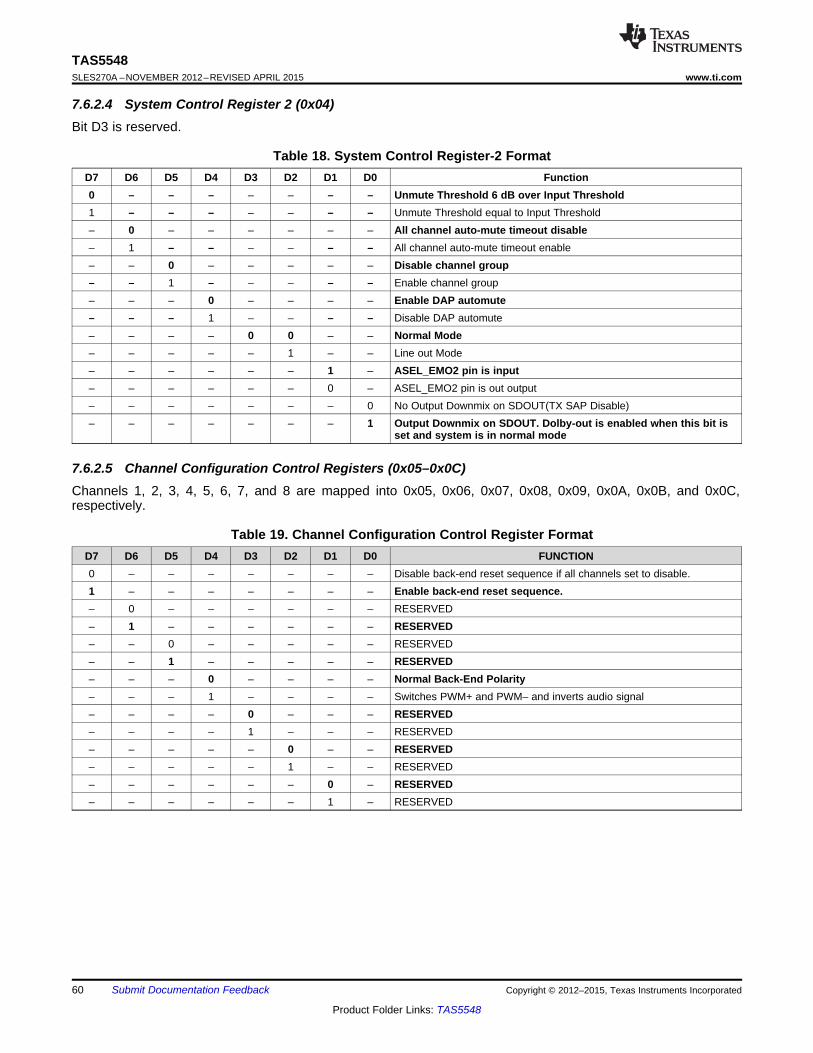
TAS5548SLES270A –NOVEMBER 2012–REVISED APRIL 2015 www.ti.com
7.6.2.4 System Control Register 2 (0x04)Bit D3 is reserved.
Table 18. System Control Register-2 FormatD7 D6 D5 D4 D3 D2 D1 D0 Function0 – – – – – – – Unmute Threshold 6 dB over Input Threshold1 – – – – – – – Unmute Threshold equal to Input Threshold– 0 – – – – – – All channel auto-mute timeout disable– 1 – – – – – – All channel auto-mute timeout enable– – 0 – – – – – Disable channel group– – 1 – – – – – Enable channel group– – – 0 – – – – Enable DAP automute– – – 1 – – – – Disable DAP automute– – – – 0 0 – – Normal Mode– – – – – 1 – – Line out Mode– – – – – – 1 – ASEL_EMO2 pin is input– – – – – – 0 – ASEL_EMO2 pin is out output– – – – – – – 0 No Output Downmix on SDOUT(TX SAP Disable)– – – – – – – 1 Output Downmix on SDOUT. Dolby-out is enabled when this bit is
set and system is in normal mode
7.6.2.5 Channel Configuration Control Registers (0x05–0x0C)Channels 1, 2, 3, 4, 5, 6, 7, and 8 are mapped into 0x05, 0x06, 0x07, 0x08, 0x09, 0x0A, 0x0B, and 0x0C,respectively.
Table 19. Channel Configuration Control Register FormatD7 D6 D5 D4 D3 D2 D1 D0 FUNCTION0 – – – – – – – Disable back-end reset sequence if all channels set to disable.1 – – – – – – – Enable back-end reset sequence.– 0 – – – – – – RESERVED– 1 – – – – – – RESERVED– – 0 – – – – – RESERVED– – 1 – – – – – RESERVED– – – 0 – – – – Normal Back-End Polarity– – – 1 – – – – Switches PWM+ and PWM– and inverts audio signal– – – – 0 – – – RESERVED– – – – 1 – – – RESERVED– – – – – 0 – – RESERVED– – – – – 1 – – RESERVED– – – – – – 0 – RESERVED– – – – – – 1 – RESERVED
60 Submit Documentation Feedback Copyright © 2012–2015, Texas Instruments Incorporated
Product Folder Links: TAS5548
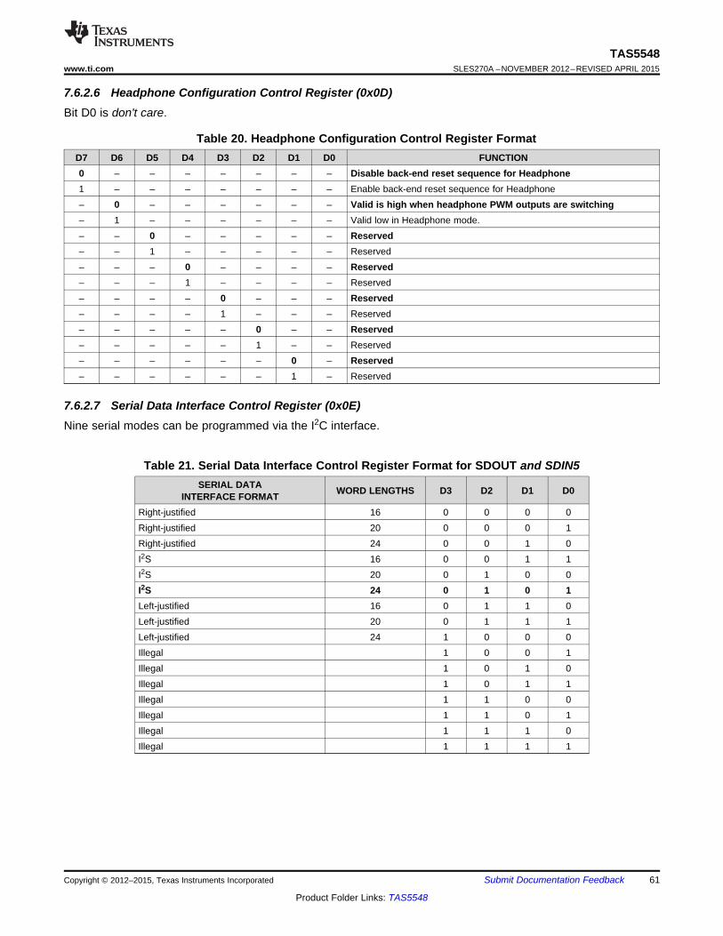
TAS5548www.ti.com SLES270A –NOVEMBER 2012–REVISED APRIL 2015
7.6.2.6 Headphone Configuration Control Register (0x0D)Bit D0 is don't care.
Table 20. Headphone Configuration Control Register FormatD7 D6 D5 D4 D3 D2 D1 D0 FUNCTION0 – – – – – – – Disable back-end reset sequence for Headphone1 – – – – – – – Enable back-end reset sequence for Headphone– 0 – – – – – – Valid is high when headphone PWM outputs are switching– 1 – – – – – – Valid low in Headphone mode.– – 0 – – – – – Reserved– – 1 – – – – – Reserved– – – 0 – – – – Reserved– – – 1 – – – – Reserved– – – – 0 – – – Reserved– – – – 1 – – – Reserved– – – – – 0 – – Reserved– – – – – 1 – – Reserved– – – – – – 0 – Reserved– – – – – – 1 – Reserved
7.6.2.7 Serial Data Interface Control Register (0x0E)Nine serial modes can be programmed via the I2C interface.
Table 21. Serial Data Interface Control Register Format for SDOUT and SDIN5SERIAL DATA WORD LENGTHS D3 D2 D1 D0INTERFACE FORMAT
Right-justified 16 0 0 0 0Right-justified 20 0 0 0 1Right-justified 24 0 0 1 0I2S 16 0 0 1 1I2S 20 0 1 0 0I2S 24 0 1 0 1Left-justified 16 0 1 1 0Left-justified 20 0 1 1 1Left-justified 24 1 0 0 0Illegal 1 0 0 1Illegal 1 0 1 0Illegal 1 0 1 1Illegal 1 1 0 0Illegal 1 1 0 1Illegal 1 1 1 0Illegal 1 1 1 1
Copyright © 2012–2015, Texas Instruments Incorporated Submit Documentation Feedback 61
Product Folder Links: TAS5548
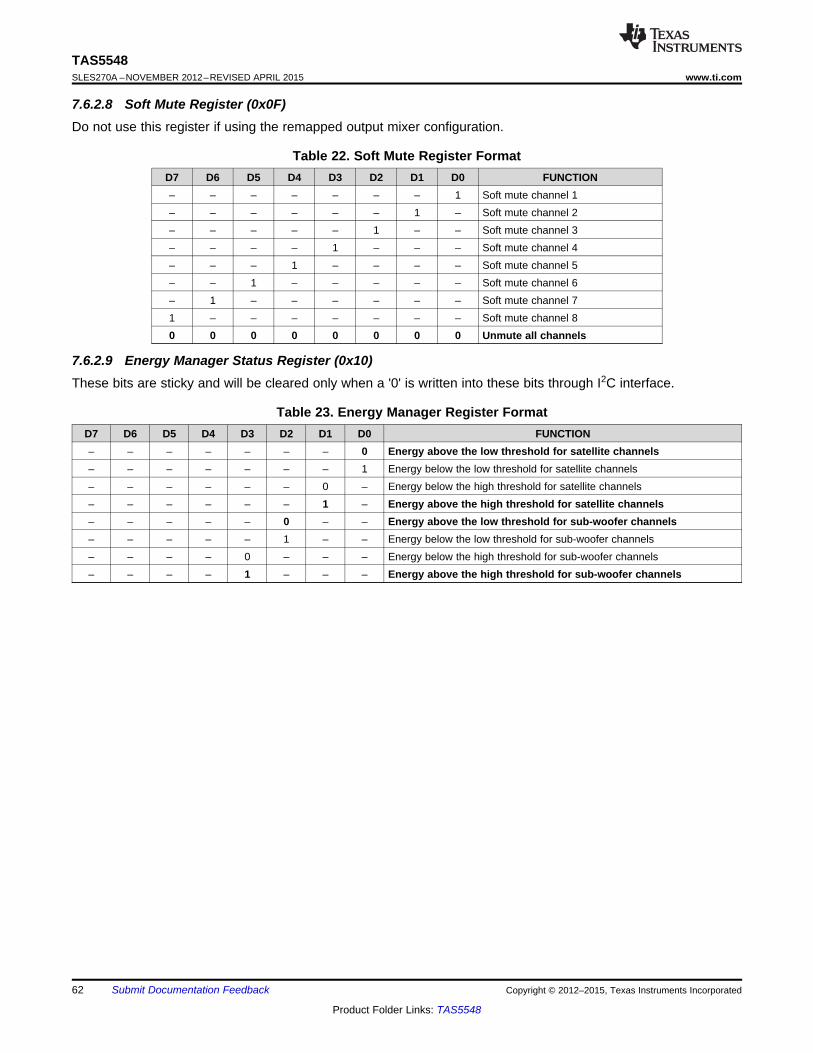
TAS5548SLES270A –NOVEMBER 2012–REVISED APRIL 2015 www.ti.com
7.6.2.8 Soft Mute Register (0x0F)Do not use this register if using the remapped output mixer configuration.
Table 22. Soft Mute Register FormatD7 D6 D5 D4 D3 D2 D1 D0 FUNCTION– – – – – – – 1 Soft mute channel 1– – – – – – 1 – Soft mute channel 2– – – – – 1 – – Soft mute channel 3– – – – 1 – – – Soft mute channel 4– – – 1 – – – – Soft mute channel 5– – 1 – – – – – Soft mute channel 6– 1 – – – – – – Soft mute channel 71 – – – – – – – Soft mute channel 80 0 0 0 0 0 0 0 Unmute all channels
7.6.2.9 Energy Manager Status Register (0x10)These bits are sticky and will be cleared only when a '0' is written into these bits through I2C interface.
Table 23. Energy Manager Register FormatD7 D6 D5 D4 D3 D2 D1 D0 FUNCTION– – – – – – – 0 Energy above the low threshold for satellite channels– – – – – – – 1 Energy below the low threshold for satellite channels– – – – – – 0 – Energy below the high threshold for satellite channels– – – – – – 1 – Energy above the high threshold for satellite channels– – – – – 0 – – Energy above the low threshold for sub-woofer channels– – – – – 1 – – Energy below the low threshold for sub-woofer channels– – – – 0 – – – Energy below the high threshold for sub-woofer channels– – – – 1 – – – Energy above the high threshold for sub-woofer channels
62 Submit Documentation Feedback Copyright © 2012–2015, Texas Instruments Incorporated
Product Folder Links: TAS5548
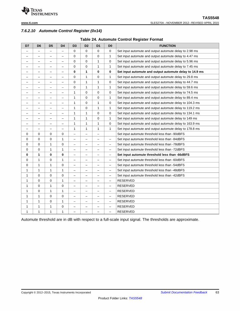
TAS5548www.ti.com SLES270A –NOVEMBER 2012–REVISED APRIL 2015
7.6.2.10 Automute Control Register (0x14)
Table 24. Automute Control Register FormatD7 D6 D5 D4 D3 D2 D1 D0 FUNCTION– – – – 0 0 0 0 Set input automute and output automute delay to 2.98 ms– – – – 0 0 0 1 Set input automute and output automute delay to 4.47 ms– – – – 0 0 1 0 Set input automute and output automute delay to 5.96 ms– – – – 0 0 1 1 Set input automute and output automute delay to 7.45 ms– – – – 0 1 0 0 Set input automute and output automute delay to 14.9 ms– – – – 0 1 0 1 Set input automute and output automute delay to 29.8 ms– – – – 0 1 1 0 Set input automute and output automute delay to 44.7 ms– – – – 0 1 1 1 Set input automute and output automute delay to 59.6 ms– – – – 1 0 0 0 Set input automute and output automute delay to 74.5 ms– – – – 1 0 0 1 Set input automute and output automute delay to 89.4 ms– – – – 1 0 1 0 Set input automute and output automute delay to 104.3 ms– – – – 1 0 1 1 Set input automute and output automute delay to 119.2 ms– – – – 1 1 0 0 Set input automute and output automute delay to 134.1 ms– – – – 1 1 0 1 Set input automute and output automute delay to 149 ms– – – – 1 1 1 0 Set input automute and output automute delay to 163.9 ms– – – – 1 1 1 1 Set input automute and output automute delay to 178.8 ms0 0 0 0 – – – Set input automute threshold less than -90dBFS0 0 0 1 – – – – Set input automute threshold less than -84dBFS0 0 1 0 – – – – Set input automute threshold less than -78dBFS0 0 1 1 – – – – Set input automute threshold less than -72dBFS0 1 0 0 – – – – Set input automute threshold less than -66dBFS0 1 0 1 – – – – Set input automute threshold less than -60dBFS0 1 1 0 – – – – Set input automute threshold less than -54dBFS1 1 1 1 – – – – Set input automute threshold less than -48dBFS1 0 0 0 – – – – Set input automute threshold less than -42dBFS1 0 0 1 – – – – RESERVED1 0 1 0 – – – – RESERVED1 0 1 1 – – – – RESERVED1 1 0 0 – – – – RESERVED1 1 0 1 – – – – RESERVED1 1 1 0 – – – – RESERVED1 1 1 1 – – – – RESERVED
Automute threshold are in dB with respect to a full-scale input signal. The thresholds are approximate.
Copyright © 2012–2015, Texas Instruments Incorporated Submit Documentation Feedback 63
Product Folder Links: TAS5548
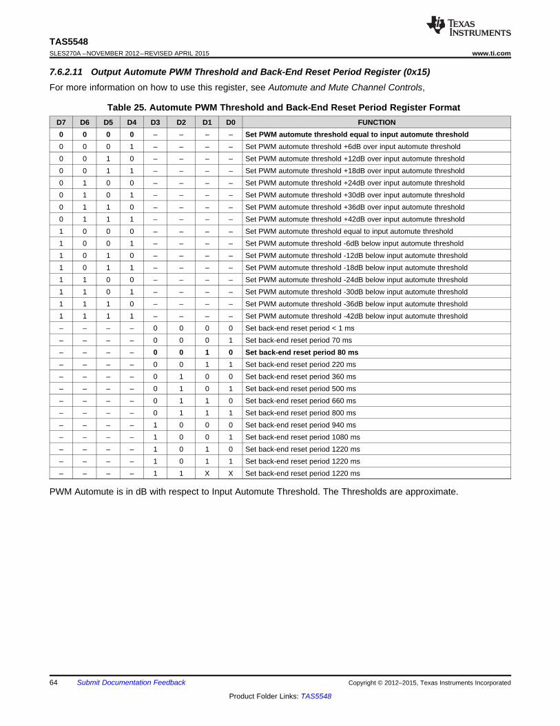
TAS5548SLES270A –NOVEMBER 2012–REVISED APRIL 2015 www.ti.com
7.6.2.11 Output Automute PWM Threshold and Back-End Reset Period Register (0x15)For more information on how to use this register, see Automute and Mute Channel Controls,
Table 25. Automute PWM Threshold and Back-End Reset Period Register FormatD7 D6 D5 D4 D3 D2 D1 D0 FUNCTION0 0 0 0 – – – – Set PWM automute threshold equal to input automute threshold0 0 0 1 – – – – Set PWM automute threshold +6dB over input automute threshold0 0 1 0 – – – – Set PWM automute threshold +12dB over input automute threshold0 0 1 1 – – – – Set PWM automute threshold +18dB over input automute threshold0 1 0 0 – – – – Set PWM automute threshold +24dB over input automute threshold0 1 0 1 – – – – Set PWM automute threshold +30dB over input automute threshold0 1 1 0 – – – – Set PWM automute threshold +36dB over input automute threshold0 1 1 1 – – – – Set PWM automute threshold +42dB over input automute threshold1 0 0 0 – – – – Set PWM automute threshold equal to input automute threshold1 0 0 1 – – – – Set PWM automute threshold -6dB below input automute threshold1 0 1 0 – – – – Set PWM automute threshold -12dB below input automute threshold1 0 1 1 – – – – Set PWM automute threshold -18dB below input automute threshold1 1 0 0 – – – – Set PWM automute threshold -24dB below input automute threshold1 1 0 1 – – – – Set PWM automute threshold -30dB below input automute threshold1 1 1 0 – – – – Set PWM automute threshold -36dB below input automute threshold1 1 1 1 – – – – Set PWM automute threshold -42dB below input automute threshold– – – – 0 0 0 0 Set back-end reset period < 1 ms– – – – 0 0 0 1 Set back-end reset period 70 ms– – – – 0 0 1 0 Set back-end reset period 80 ms– – – – 0 0 1 1 Set back-end reset period 220 ms– – – – 0 1 0 0 Set back-end reset period 360 ms– – – – 0 1 0 1 Set back-end reset period 500 ms– – – – 0 1 1 0 Set back-end reset period 660 ms– – – – 0 1 1 1 Set back-end reset period 800 ms– – – – 1 0 0 0 Set back-end reset period 940 ms– – – – 1 0 0 1 Set back-end reset period 1080 ms– – – – 1 0 1 0 Set back-end reset period 1220 ms– – – – 1 0 1 1 Set back-end reset period 1220 ms– – – – 1 1 X X Set back-end reset period 1220 ms
PWM Automute is in dB with respect to Input Automute Threshold. The Thresholds are approximate.
64 Submit Documentation Feedback Copyright © 2012–2015, Texas Instruments Incorporated
Product Folder Links: TAS5548
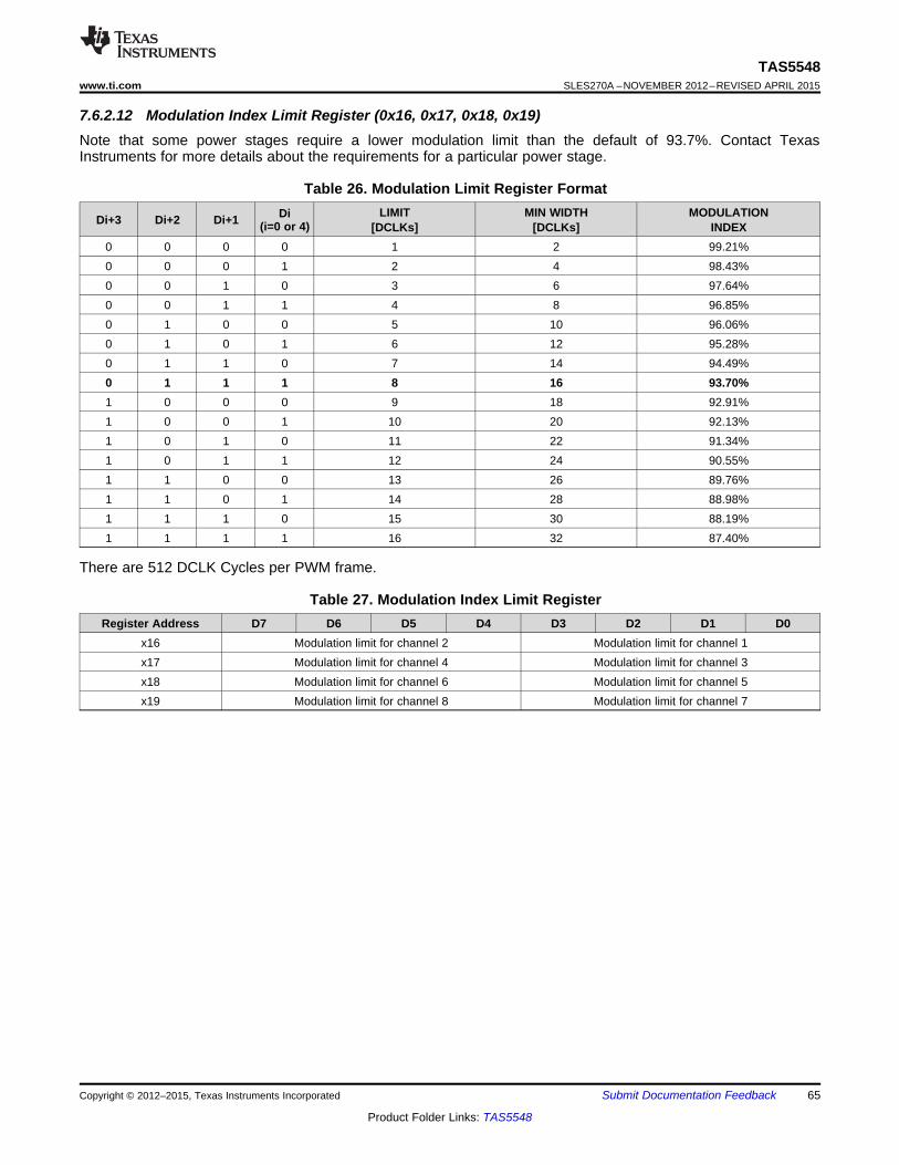
TAS5548www.ti.com SLES270A –NOVEMBER 2012–REVISED APRIL 2015
7.6.2.12 Modulation Index Limit Register (0x16, 0x17, 0x18, 0x19)Note that some power stages require a lower modulation limit than the default of 93.7%. Contact TexasInstruments for more details about the requirements for a particular power stage.
Table 26. Modulation Limit Register FormatLIMIT MIN WIDTH MODULATIONDiDi+3 Di+2 Di+1 (i=0 or 4) [DCLKs] [DCLKs] INDEX
0 0 0 0 1 2 99.21%0 0 0 1 2 4 98.43%0 0 1 0 3 6 97.64%0 0 1 1 4 8 96.85%0 1 0 0 5 10 96.06%0 1 0 1 6 12 95.28%0 1 1 0 7 14 94.49%0 1 1 1 8 16 93.70%1 0 0 0 9 18 92.91%1 0 0 1 10 20 92.13%1 0 1 0 11 22 91.34%1 0 1 1 12 24 90.55%1 1 0 0 13 26 89.76%1 1 0 1 14 28 88.98%1 1 1 0 15 30 88.19%1 1 1 1 16 32 87.40%
There are 512 DCLK Cycles per PWM frame.
Table 27. Modulation Index Limit RegisterRegister Address D7 D6 D5 D4 D3 D2 D1 D0
x16 Modulation limit for channel 2 Modulation limit for channel 1x17 Modulation limit for channel 4 Modulation limit for channel 3x18 Modulation limit for channel 6 Modulation limit for channel 5x19 Modulation limit for channel 8 Modulation limit for channel 7
Copyright © 2012–2015, Texas Instruments Incorporated Submit Documentation Feedback 65
Product Folder Links: TAS5548
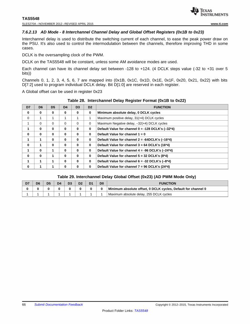
TAS5548SLES270A –NOVEMBER 2012–REVISED APRIL 2015 www.ti.com
7.6.2.13 AD Mode - 8 Interchannel Channel Delay and Global Offset Registers (0x1B to 0x23)Interchannel delay is used to distribute the switching current of each channel, to ease the peak power draw onthe PSU. It's also used to control the intermodulation between the channels, therefore improving THD in somecases.
DCLK is the oversampling clock of the PWM.
DCLK on the TAS5548 will be constant, unless some AM avoidance modes are used.
Each channel can have its channel delay set between -128 to +124. (4 DCLK steps value (-32 to +31 over 5bits))
Channels 0, 1, 2, 3, 4, 5, 6, 7 are mapped into (0x1B, 0x1C, 0x1D, 0x1E, 0x1F, 0x20, 0x21, 0x22) with bitsD[7:2] used to program individual DCLK delay. Bit D[1:0] are reserved in each register.
A Global offset can be used in register 0x23
Table 28. Interchannel Delay Register Format (0x1B to 0x22)D7 D6 D5 D4 D3 D2 FUNCTION0 0 0 0 0 0 Minimum absolute delay, 0 DCLK cycles0 1 1 1 1 1 Maximum positive delay, 31(×4) DCLK cycles1 0 0 0 0 0 Maximum Negative delay, –32(×4) DCLK cycles1 0 0 0 0 0 Default Value for channel 0 = -128 DCLK's (–32*4)0 0 0 0 0 0 Default Value for channel 1 = 01 1 0 0 0 0 Default Value for channel 2 = -64DCLK's (–16*4)0 1 0 0 0 0 Default Value for channel 3 = 64 DCLK's (16*4)1 0 1 0 0 0 Default Value for channel 4 = -96 DCLK's (–24*4)0 0 1 0 0 0 Default Value for channel 5 = 32 DCLK's (8*4)1 1 1 0 0 0 Default Value for channel 6 = -32 DCLK's (–8*4)0 1 1 0 0 0 Default Value for channel 7 = 96 DCLK's (24*4)
Table 29. Interchannel Delay Global Offset (0x23) (AD PWM Mode Only)D7 D6 D5 D4 D3 D2 D1 D0 FUNCTION0 0 0 0 0 0 0 0 Minimum absolute offset, 0 DCLK cycles, Default for channel 01 1 1 1 1 1 1 1 Maximum absolute delay, 255 DCLK cycles
66 Submit Documentation Feedback Copyright © 2012–2015, Texas Instruments Incorporated
Product Folder Links: TAS5548
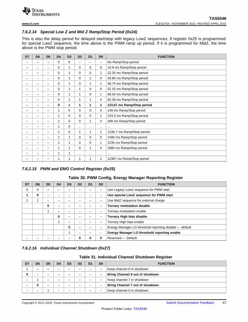
TAS5548www.ti.com SLES270A –NOVEMBER 2012–REVISED APRIL 2015
7.6.2.14 Special Low Z and Mid Z Ramp/Stop Period (0x24)This is also the delay period for delayed start/stop with legacy LowZ sequences. If register 0x25 is programmedfor special LowZ sequence, the time above is the PWM ramp up period. If it is programmed for MidZ, the timeabove is the PWM stop period.
D7 D6 D5 D4 D3 D2 D1 D0 FUNCTION– – – 0 0 – – – No Ramp/Stop period– – – 0 1 0 0 0 14.9 ms Ramp/Stop period– – – 0 1 0 0 1 22.35 ms Ramp/Stop period– – – 0 1 0 1 0 29.80 ms Ramp/Stop period– – – 0 1 0 1 1 38.74 ms Ramp/Stop period– – – 0 1 1 0 0 52.15 ms Ramp/Stop period– – – 0 1 1 0 1 68.54 ms Ramp/Stop period– – – 0 1 1 1 0 92.38 ms Ramp/Stop period– – – 0 1 1 1 1 123.67 ms Ramp/Stop period– – – 1 0 0 0 0 149 ms Ramp/Stop period– – – 1 0 0 0 1 223.5 ms Ramp/Stop period– – – 1 0 0 1 0 298 ms Ramp/Stop period– – – 1 0 .. .. .. …– – – 1 0 1 1 1 1236.7 ms Ramp/Stop period– – – 1 1 0 0 0 1490 ms Ramp/Stop period– – – 1 1 0 0 1 2235 ms Ramp/Stop period– – – 1 1 0 1 0 2980 ms Ramp/Stop period– – – 1 1 .. .. .. …– – – 1 1 1 1 1 12367 ms Ramp/Stop period
7.6.2.15 PWM and EMO Control Register (0x25)
Table 30. PWM Config, Energy Manager Reporting RegisterD7 D6 D5 D4 D3 D2 D1 D0 FUNCTION0 0 – – – – – – Use Legacy LowZ sequence for PWM start1 0 – – – – – – Use special LowZ sequence for PWM start1 1 – – – – – – Use MidZ sequence for external charge
0 – – – – – Ternary modulation disable1 – – – – – Ternary modulation enable
0 – – – – Ternary High bias disable1 – – – – Ternary High bias enable
0 – – – Energy Manager LO threshold reporting disable ← default1 – – – Energy Manager LO threshold reporting enable
– – – – – 0 0 0 Reserved ← Default
7.6.2.16 Individual Channel Shutdown (0x27)
Table 31. Individual Channel Shutdown RegisterD7 D6 D5 D4 D3 D2 D1 D0 FUNCTION1 – – – – – – – Keep channel 8 in shutdown0 – – – – – – – Bring Channel 8 out of shutdown– 1 – – – – – – Keep channel 7 in shutdown– 0 – – – – – – Bring Channel 7 out of shutdown– – 1 – – – – – Keep channel 6 in shutdown
Copyright © 2012–2015, Texas Instruments Incorporated Submit Documentation Feedback 67
Product Folder Links: TAS5548
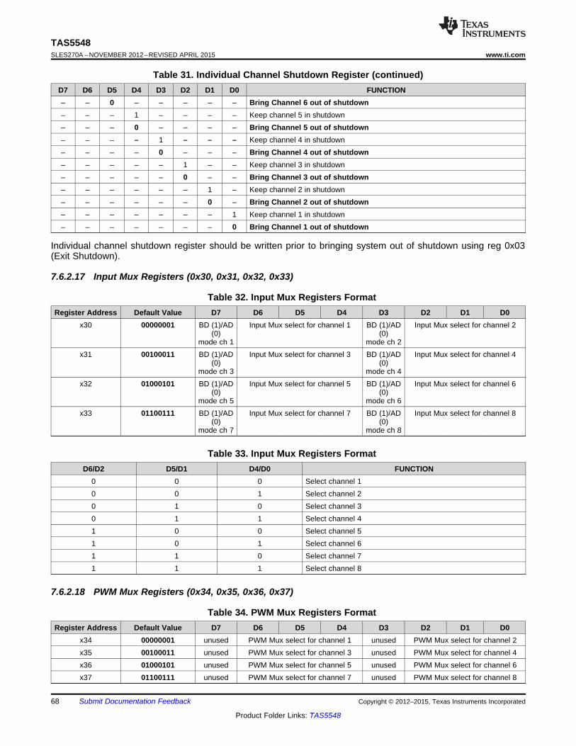
TAS5548SLES270A –NOVEMBER 2012–REVISED APRIL 2015 www.ti.com
Table 31. Individual Channel Shutdown Register (continued)D7 D6 D5 D4 D3 D2 D1 D0 FUNCTION– – 0 – – – – – Bring Channel 6 out of shutdown– – – 1 – – – – Keep channel 5 in shutdown– – – 0 – – – – Bring Channel 5 out of shutdown– – – – 1 – – – Keep channel 4 in shutdown– – – – 0 – – – Bring Channel 4 out of shutdown– – – – – 1 – – Keep channel 3 in shutdown– – – – – 0 – – Bring Channel 3 out of shutdown– – – – – – 1 – Keep channel 2 in shutdown– – – – – – 0 – Bring Channel 2 out of shutdown– – – – – – – 1 Keep channel 1 in shutdown– – – – – – – 0 Bring Channel 1 out of shutdown
Individual channel shutdown register should be written prior to bringing system out of shutdown using reg 0x03(Exit Shutdown).
7.6.2.17 Input Mux Registers (0x30, 0x31, 0x32, 0x33)
Table 32. Input Mux Registers FormatRegister Address Default Value D7 D6 D5 D4 D3 D2 D1 D0
x30 00000001 BD (1)/AD Input Mux select for channel 1 BD (1)/AD Input Mux select for channel 2(0) (0)
mode ch 1 mode ch 2x31 00100011 BD (1)/AD Input Mux select for channel 3 BD (1)/AD Input Mux select for channel 4
(0) (0)mode ch 3 mode ch 4
x32 01000101 BD (1)/AD Input Mux select for channel 5 BD (1)/AD Input Mux select for channel 6(0) (0)
mode ch 5 mode ch 6x33 01100111 BD (1)/AD Input Mux select for channel 7 BD (1)/AD Input Mux select for channel 8
(0) (0)mode ch 7 mode ch 8
Table 33. Input Mux Registers FormatD6/D2 D5/D1 D4/D0 FUNCTION
0 0 0 Select channel 10 0 1 Select channel 20 1 0 Select channel 30 1 1 Select channel 41 0 0 Select channel 51 0 1 Select channel 61 1 0 Select channel 71 1 1 Select channel 8
7.6.2.18 PWM Mux Registers (0x34, 0x35, 0x36, 0x37)
Table 34. PWM Mux Registers FormatRegister Address Default Value D7 D6 D5 D4 D3 D2 D1 D0
x34 00000001 unused PWM Mux select for channel 1 unused PWM Mux select for channel 2x35 00100011 unused PWM Mux select for channel 3 unused PWM Mux select for channel 4x36 01000101 unused PWM Mux select for channel 5 unused PWM Mux select for channel 6x37 01100111 unused PWM Mux select for channel 7 unused PWM Mux select for channel 8
68 Submit Documentation Feedback Copyright © 2012–2015, Texas Instruments Incorporated
Product Folder Links: TAS5548
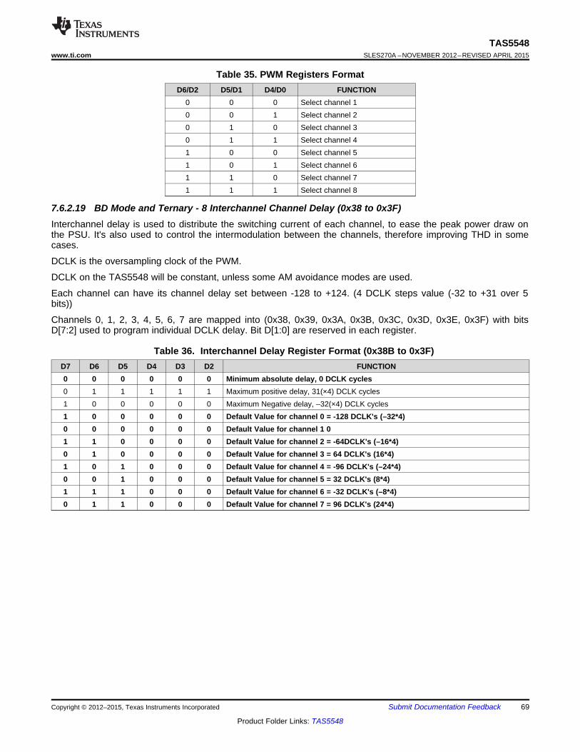
TAS5548www.ti.com SLES270A –NOVEMBER 2012–REVISED APRIL 2015
Table 35. PWM Registers FormatD6/D2 D5/D1 D4/D0 FUNCTION
0 0 0 Select channel 10 0 1 Select channel 20 1 0 Select channel 30 1 1 Select channel 41 0 0 Select channel 51 0 1 Select channel 61 1 0 Select channel 71 1 1 Select channel 8
7.6.2.19 BD Mode and Ternary - 8 Interchannel Channel Delay (0x38 to 0x3F)Interchannel delay is used to distribute the switching current of each channel, to ease the peak power draw onthe PSU. It's also used to control the intermodulation between the channels, therefore improving THD in somecases.
DCLK is the oversampling clock of the PWM.
DCLK on the TAS5548 will be constant, unless some AM avoidance modes are used.
Each channel can have its channel delay set between -128 to +124. (4 DCLK steps value (-32 to +31 over 5bits))
Channels 0, 1, 2, 3, 4, 5, 6, 7 are mapped into (0x38, 0x39, 0x3A, 0x3B, 0x3C, 0x3D, 0x3E, 0x3F) with bitsD[7:2] used to program individual DCLK delay. Bit D[1:0] are reserved in each register.
Table 36. Interchannel Delay Register Format (0x38B to 0x3F)D7 D6 D5 D4 D3 D2 FUNCTION0 0 0 0 0 0 Minimum absolute delay, 0 DCLK cycles0 1 1 1 1 1 Maximum positive delay, 31(×4) DCLK cycles1 0 0 0 0 0 Maximum Negative delay, –32(×4) DCLK cycles1 0 0 0 0 0 Default Value for channel 0 = -128 DCLK's (–32*4)0 0 0 0 0 0 Default Value for channel 1 01 1 0 0 0 0 Default Value for channel 2 = -64DCLK's (–16*4)0 1 0 0 0 0 Default Value for channel 3 = 64 DCLK's (16*4)1 0 1 0 0 0 Default Value for channel 4 = -96 DCLK's (–24*4)0 0 1 0 0 0 Default Value for channel 5 = 32 DCLK's (8*4)1 1 1 0 0 0 Default Value for channel 6 = -32 DCLK's (–8*4)0 1 1 0 0 0 Default Value for channel 7 = 96 DCLK's (24*4)
Copyright © 2012–2015, Texas Instruments Incorporated Submit Documentation Feedback 69
Product Folder Links: TAS5548
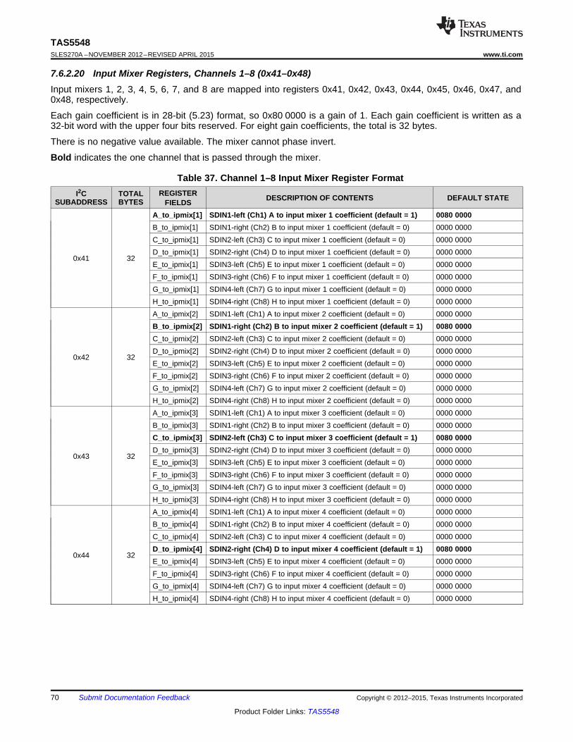
TAS5548SLES270A –NOVEMBER 2012–REVISED APRIL 2015 www.ti.com
7.6.2.20 Input Mixer Registers, Channels 1–8 (0x41–0x48)Input mixers 1, 2, 3, 4, 5, 6, 7, and 8 are mapped into registers 0x41, 0x42, 0x43, 0x44, 0x45, 0x46, 0x47, and0x48, respectively.
Each gain coefficient is in 28-bit (5.23) format, so 0x80 0000 is a gain of 1. Each gain coefficient is written as a32-bit word with the upper four bits reserved. For eight gain coefficients, the total is 32 bytes.
There is no negative value available. The mixer cannot phase invert.
Bold indicates the one channel that is passed through the mixer.
Table 37. Channel 1–8 Input Mixer Register FormatREGISTERI2C TOTAL DESCRIPTION OF CONTENTS DEFAULT STATESUBADDRESS BYTES FIELDS
A_to_ipmix[1] SDIN1-left (Ch1) A to input mixer 1 coefficient (default = 1) 0080 0000B_to_ipmix[1] SDIN1-right (Ch2) B to input mixer 1 coefficient (default = 0) 0000 0000C_to_ipmix[1] SDIN2-left (Ch3) C to input mixer 1 coefficient (default = 0) 0000 0000D_to_ipmix[1] SDIN2-right (Ch4) D to input mixer 1 coefficient (default = 0) 0000 0000
0x41 32E_to_ipmix[1] SDIN3-left (Ch5) E to input mixer 1 coefficient (default = 0) 0000 0000F_to_ipmix[1] SDIN3-right (Ch6) F to input mixer 1 coefficient (default = 0) 0000 0000G_to_ipmix[1] SDIN4-left (Ch7) G to input mixer 1 coefficient (default = 0) 0000 0000H_to_ipmix[1] SDIN4-right (Ch8) H to input mixer 1 coefficient (default = 0) 0000 0000A_to_ipmix[2] SDIN1-left (Ch1) A to input mixer 2 coefficient (default = 0) 0000 0000B_to_ipmix[2] SDIN1-right (Ch2) B to input mixer 2 coefficient (default = 1) 0080 0000C_to_ipmix[2] SDIN2-left (Ch3) C to input mixer 2 coefficient (default = 0) 0000 0000D_to_ipmix[2] SDIN2-right (Ch4) D to input mixer 2 coefficient (default = 0) 0000 0000
0x42 32E_to_ipmix[2] SDIN3-left (Ch5) E to input mixer 2 coefficient (default = 0) 0000 0000F_to_ipmix[2] SDIN3-right (Ch6) F to input mixer 2 coefficient (default = 0) 0000 0000G_to_ipmix[2] SDIN4-left (Ch7) G to input mixer 2 coefficient (default = 0) 0000 0000H_to_ipmix[2] SDIN4-right (Ch8) H to input mixer 2 coefficient (default = 0) 0000 0000A_to_ipmix[3] SDIN1-left (Ch1) A to input mixer 3 coefficient (default = 0) 0000 0000B_to_ipmix[3] SDIN1-right (Ch2) B to input mixer 3 coefficient (default = 0) 0000 0000C_to_ipmix[3] SDIN2-left (Ch3) C to input mixer 3 coefficient (default = 1) 0080 0000D_to_ipmix[3] SDIN2-right (Ch4) D to input mixer 3 coefficient (default = 0) 0000 0000
0x43 32E_to_ipmix[3] SDIN3-left (Ch5) E to input mixer 3 coefficient (default = 0) 0000 0000F_to_ipmix[3] SDIN3-right (Ch6) F to input mixer 3 coefficient (default = 0) 0000 0000G_to_ipmix[3] SDIN4-left (Ch7) G to input mixer 3 coefficient (default = 0) 0000 0000H_to_ipmix[3] SDIN4-right (Ch8) H to input mixer 3 coefficient (default = 0) 0000 0000A_to_ipmix[4] SDIN1-left (Ch1) A to input mixer 4 coefficient (default = 0) 0000 0000B_to_ipmix[4] SDIN1-right (Ch2) B to input mixer 4 coefficient (default = 0) 0000 0000C_to_ipmix[4] SDIN2-left (Ch3) C to input mixer 4 coefficient (default = 0) 0000 0000D_to_ipmix[4] SDIN2-right (Ch4) D to input mixer 4 coefficient (default = 1) 0080 0000
0x44 32E_to_ipmix[4] SDIN3-left (Ch5) E to input mixer 4 coefficient (default = 0) 0000 0000F_to_ipmix[4] SDIN3-right (Ch6) F to input mixer 4 coefficient (default = 0) 0000 0000G_to_ipmix[4] SDIN4-left (Ch7) G to input mixer 4 coefficient (default = 0) 0000 0000H_to_ipmix[4] SDIN4-right (Ch8) H to input mixer 4 coefficient (default = 0) 0000 0000
70 Submit Documentation Feedback Copyright © 2012–2015, Texas Instruments Incorporated
Product Folder Links: TAS5548
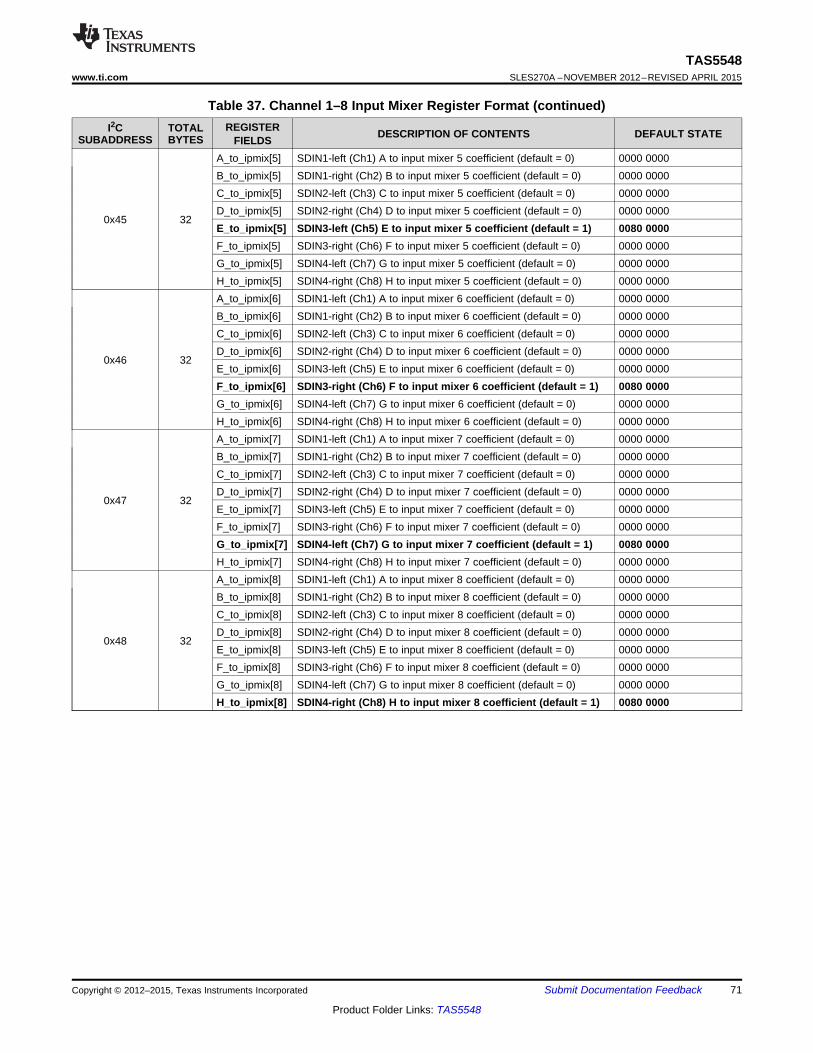
TAS5548www.ti.com SLES270A –NOVEMBER 2012–REVISED APRIL 2015
Table 37. Channel 1–8 Input Mixer Register Format (continued)REGISTERI2C TOTAL DESCRIPTION OF CONTENTS DEFAULT STATESUBADDRESS BYTES FIELDS
A_to_ipmix[5] SDIN1-left (Ch1) A to input mixer 5 coefficient (default = 0) 0000 0000B_to_ipmix[5] SDIN1-right (Ch2) B to input mixer 5 coefficient (default = 0) 0000 0000C_to_ipmix[5] SDIN2-left (Ch3) C to input mixer 5 coefficient (default = 0) 0000 0000D_to_ipmix[5] SDIN2-right (Ch4) D to input mixer 5 coefficient (default = 0) 0000 0000
0x45 32E_to_ipmix[5] SDIN3-left (Ch5) E to input mixer 5 coefficient (default = 1) 0080 0000F_to_ipmix[5] SDIN3-right (Ch6) F to input mixer 5 coefficient (default = 0) 0000 0000G_to_ipmix[5] SDIN4-left (Ch7) G to input mixer 5 coefficient (default = 0) 0000 0000H_to_ipmix[5] SDIN4-right (Ch8) H to input mixer 5 coefficient (default = 0) 0000 0000A_to_ipmix[6] SDIN1-left (Ch1) A to input mixer 6 coefficient (default = 0) 0000 0000B_to_ipmix[6] SDIN1-right (Ch2) B to input mixer 6 coefficient (default = 0) 0000 0000C_to_ipmix[6] SDIN2-left (Ch3) C to input mixer 6 coefficient (default = 0) 0000 0000D_to_ipmix[6] SDIN2-right (Ch4) D to input mixer 6 coefficient (default = 0) 0000 0000
0x46 32E_to_ipmix[6] SDIN3-left (Ch5) E to input mixer 6 coefficient (default = 0) 0000 0000F_to_ipmix[6] SDIN3-right (Ch6) F to input mixer 6 coefficient (default = 1) 0080 0000G_to_ipmix[6] SDIN4-left (Ch7) G to input mixer 6 coefficient (default = 0) 0000 0000H_to_ipmix[6] SDIN4-right (Ch8) H to input mixer 6 coefficient (default = 0) 0000 0000A_to_ipmix[7] SDIN1-left (Ch1) A to input mixer 7 coefficient (default = 0) 0000 0000B_to_ipmix[7] SDIN1-right (Ch2) B to input mixer 7 coefficient (default = 0) 0000 0000C_to_ipmix[7] SDIN2-left (Ch3) C to input mixer 7 coefficient (default = 0) 0000 0000D_to_ipmix[7] SDIN2-right (Ch4) D to input mixer 7 coefficient (default = 0) 0000 0000
0x47 32E_to_ipmix[7] SDIN3-left (Ch5) E to input mixer 7 coefficient (default = 0) 0000 0000F_to_ipmix[7] SDIN3-right (Ch6) F to input mixer 7 coefficient (default = 0) 0000 0000G_to_ipmix[7] SDIN4-left (Ch7) G to input mixer 7 coefficient (default = 1) 0080 0000H_to_ipmix[7] SDIN4-right (Ch8) H to input mixer 7 coefficient (default = 0) 0000 0000A_to_ipmix[8] SDIN1-left (Ch1) A to input mixer 8 coefficient (default = 0) 0000 0000B_to_ipmix[8] SDIN1-right (Ch2) B to input mixer 8 coefficient (default = 0) 0000 0000C_to_ipmix[8] SDIN2-left (Ch3) C to input mixer 8 coefficient (default = 0) 0000 0000D_to_ipmix[8] SDIN2-right (Ch4) D to input mixer 8 coefficient (default = 0) 0000 0000
0x48 32E_to_ipmix[8] SDIN3-left (Ch5) E to input mixer 8 coefficient (default = 0) 0000 0000F_to_ipmix[8] SDIN3-right (Ch6) F to input mixer 8 coefficient (default = 0) 0000 0000G_to_ipmix[8] SDIN4-left (Ch7) G to input mixer 8 coefficient (default = 0) 0000 0000H_to_ipmix[8] SDIN4-right (Ch8) H to input mixer 8 coefficient (default = 1) 0080 0000
Copyright © 2012–2015, Texas Instruments Incorporated Submit Documentation Feedback 71
Product Folder Links: TAS5548
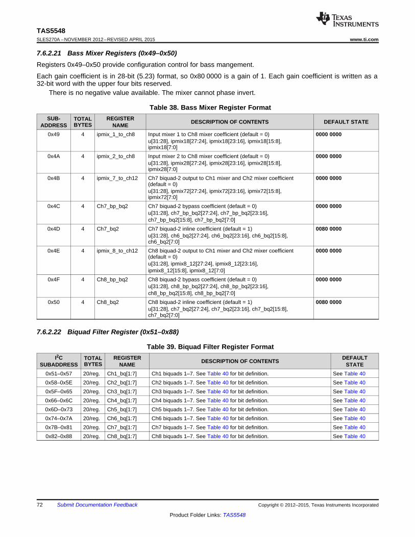
TAS5548SLES270A –NOVEMBER 2012–REVISED APRIL 2015 www.ti.com
7.6.2.21 Bass Mixer Registers (0x49–0x50)Registers 0x49–0x50 provide configuration control for bass mangement.
Each gain coefficient is in 28-bit (5.23) format, so 0x80 0000 is a gain of 1. Each gain coefficient is written as a32-bit word with the upper four bits reserved.
There is no negative value available. The mixer cannot phase invert.
Table 38. Bass Mixer Register FormatSUB- REGISTERTOTAL DESCRIPTION OF CONTENTS DEFAULT STATEBYTESADDRESS NAME0x49 4 ipmix_1_to_ch8 Input mixer 1 to Ch8 mixer coefficient (default = 0) 0000 0000
u[31:28], ipmix18[27:24], ipmix18[23:16], ipmix18[15:8],ipmix18[7:0]
0x4A 4 ipmix_2_to_ch8 Input mixer 2 to Ch8 mixer coefficient (default = 0) 0000 0000u[31:28], ipmix28[27:24], ipmix28[23:16], ipmix28[15:8],ipmix28[7:0]
0x4B 4 ipmix_7_to_ch12 Ch7 biquad-2 output to Ch1 mixer and Ch2 mixer coefficient 0000 0000(default = 0)u[31:28], ipmix72[27:24], ipmix72[23:16], ipmix72[15:8],ipmix72[7:0]
0x4C 4 Ch7_bp_bq2 Ch7 biquad-2 bypass coefficient (default = 0) 0000 0000u[31:28], ch7_bp_bq2[27:24], ch7_bp_bq2[23:16],ch7_bp_bq2[15:8], ch7_bp_bq2[7:0]
0x4D 4 Ch7_bq2 Ch7 biquad-2 inline coefficient (default = 1) 0080 0000u[31:28], ch6_bq2[27:24], ch6_bq2[23:16], ch6_bq2[15:8],ch6_bq2[7:0]
0x4E 4 ipmix_8_to_ch12 Ch8 biquad-2 output to Ch1 mixer and Ch2 mixer coefficient 0000 0000(default = 0)u[31:28], ipmix8_12[27:24], ipmix8_12[23:16],ipmix8_12[15:8], ipmix8_12[7:0]
0x4F 4 Ch8_bp_bq2 Ch8 biquad-2 bypass coefficient (default = 0) 0000 0000u[31:28], ch8_bp_bq2[27:24], ch8_bp_bq2[23:16],ch8_bp_bq2[15:8], ch8_bp_bq2[7:0]
0x50 4 Ch8_bq2 Ch8 biquad-2 inline coefficient (default = 1) 0080 0000u[31:28], ch7_bq2[27:24], ch7_bq2[23:16], ch7_bq2[15:8],ch7_bq2[7:0]
7.6.2.22 Biquad Filter Register (0x51–0x88)
Table 39. Biquad Filter Register FormatI2C REGISTER DEFAULTTOTAL DESCRIPTION OF CONTENTSBYTESSUBADDRESS NAME STATE
0x51–0x57 20/reg. Ch1_bq[1:7] Ch1 biquads 1–7. See Table 40 for bit definition. See Table 400x58–0x5E 20/reg. Ch2_bq[1:7] Ch2 biquads 1–7. See Table 40 for bit definition. See Table 400x5F–0x65 20/reg. Ch3_bq[1:7] Ch3 biquads 1–7. See Table 40 for bit definition. See Table 400x66–0x6C 20/reg. Ch4_bq[1:7] Ch4 biquads 1–7. See Table 40 for bit definition. See Table 400x6D–0x73 20/reg. Ch5_bq[1:7] Ch5 biquads 1–7. See Table 40 for bit definition. See Table 400x74–0x7A 20/reg. Ch6_bq[1:7] Ch6 biquads 1–7. See Table 40 for bit definition. See Table 400x7B–0x81 20/reg. Ch7_bq[1:7] Ch7 biquads 1–7. See Table 40 for bit definition. See Table 400x82–0x88 20/reg. Ch8_bq[1:7] Ch8 biquads 1–7. See Table 40 for bit definition. See Table 40
72 Submit Documentation Feedback Copyright © 2012–2015, Texas Instruments Incorporated
Product Folder Links: TAS5548
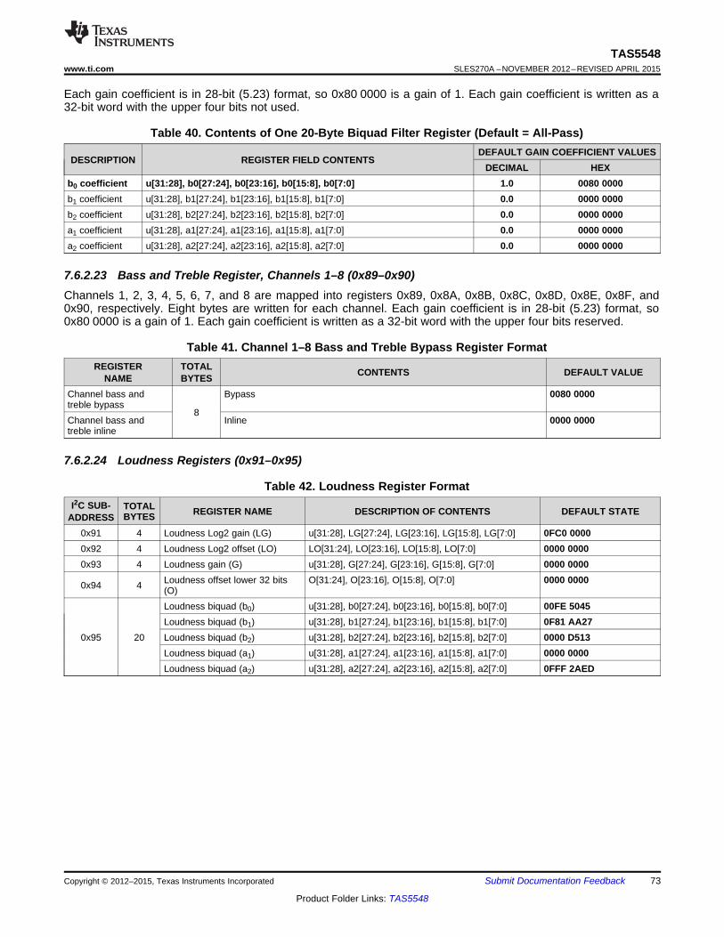
TAS5548www.ti.com SLES270A –NOVEMBER 2012–REVISED APRIL 2015
Each gain coefficient is in 28-bit (5.23) format, so 0x80 0000 is a gain of 1. Each gain coefficient is written as a32-bit word with the upper four bits not used.
Table 40. Contents of One 20-Byte Biquad Filter Register (Default = All-Pass)DEFAULT GAIN COEFFICIENT VALUES
DESCRIPTION REGISTER FIELD CONTENTSDECIMAL HEX
b0 coefficient u[31:28], b0[27:24], b0[23:16], b0[15:8], b0[7:0] 1.0 0080 0000b1 coefficient u[31:28], b1[27:24], b1[23:16], b1[15:8], b1[7:0] 0.0 0000 0000b2 coefficient u[31:28], b2[27:24], b2[23:16], b2[15:8], b2[7:0] 0.0 0000 0000a1 coefficient u[31:28], a1[27:24], a1[23:16], a1[15:8], a1[7:0] 0.0 0000 0000a2 coefficient u[31:28], a2[27:24], a2[23:16], a2[15:8], a2[7:0] 0.0 0000 0000
7.6.2.23 Bass and Treble Register, Channels 1–8 (0x89–0x90)Channels 1, 2, 3, 4, 5, 6, 7, and 8 are mapped into registers 0x89, 0x8A, 0x8B, 0x8C, 0x8D, 0x8E, 0x8F, and0x90, respectively. Eight bytes are written for each channel. Each gain coefficient is in 28-bit (5.23) format, so0x80 0000 is a gain of 1. Each gain coefficient is written as a 32-bit word with the upper four bits reserved.
Table 41. Channel 1–8 Bass and Treble Bypass Register FormatREGISTER TOTAL CONTENTS DEFAULT VALUENAME BYTES
Channel bass and Bypass 0080 0000treble bypass
8Channel bass and Inline 0000 0000treble inline
7.6.2.24 Loudness Registers (0x91–0x95)
Table 42. Loudness Register FormatI2C SUB- TOTAL REGISTER NAME DESCRIPTION OF CONTENTS DEFAULT STATEBYTESADDRESS
0x91 4 Loudness Log2 gain (LG) u[31:28], LG[27:24], LG[23:16], LG[15:8], LG[7:0] 0FC0 00000x92 4 Loudness Log2 offset (LO) LO[31:24], LO[23:16], LO[15:8], LO[7:0] 0000 00000x93 4 Loudness gain (G) u[31:28], G[27:24], G[23:16], G[15:8], G[7:0] 0000 0000
Loudness offset lower 32 bits O[31:24], O[23:16], O[15:8], O[7:0] 0000 00000x94 4 (O)Loudness biquad (b0) u[31:28], b0[27:24], b0[23:16], b0[15:8], b0[7:0] 00FE 5045Loudness biquad (b1) u[31:28], b1[27:24], b1[23:16], b1[15:8], b1[7:0] 0F81 AA27
0x95 20 Loudness biquad (b2) u[31:28], b2[27:24], b2[23:16], b2[15:8], b2[7:0] 0000 D513Loudness biquad (a1) u[31:28], a1[27:24], a1[23:16], a1[15:8], a1[7:0] 0000 0000Loudness biquad (a2) u[31:28], a2[27:24], a2[23:16], a2[15:8], a2[7:0] 0FFF 2AED
Copyright © 2012–2015, Texas Instruments Incorporated Submit Documentation Feedback 73
Product Folder Links: TAS5548
TAS5548SLES270A –NOVEMBER 2012–REVISED APRIL 2015 www.ti.com
7.6.2.25 DRC1 Control Register CH1-7 (0x96) – WriteDRC Control selects which channels contribute to the expansion/compression evaluation using DRC1. Theevaluation is global such that if one signal forces compression all DRC1 signals will be in compression.
Table 43. Write Register FormatD31 D30 D29 D28 D27 D26 D25 D24 FUNCTION
x x x x x x x x
D23 D22 D21 D20 D19 D18 D17 D16 FUNCTIONx x x x x x x x
D15 D14 D13 D12 D11 D10 D9 D8 FUNCTIONx x – – – – – –– – 0 0 – – – – Channel 7: Not Included in DRC evaluation– – 0 1 – – – – Channel 7: Pre-volume DRC evaluation– – 1 0 – – – – Channel 7: Post-volume DRC evaluation– – 1 1 – – – – Channel 7: Not Included in DRC evaluation– – – – 0 0 – – Channel 6: Not Included in DRC evaluation– – – – 0 1 – – Channel 6: Pre-volume DRC evaluation– – – – 1 0 – – Channel 6: Post-volume DRC evaluation– – – – 1 1 – – Channel 6: Not Included in DRC evaluation– – – – – – 0 0 Channel 5: Not Included in DRC evaluation– – – – – – 0 1 Channel 5: Pre-volume DRC evaluation– – – – – – 1 0 Channel 5: Post-volume DRC evaluation– – – – – – 1 1 Channel 5: Not Included in DRC evaluation
D7 D6 D5 D4 D3 D2 D1 D0 FUNCTION0 0 – – – – – – Channel 4: Not Included in DRC evaluation0 1 – – – – – – Channel 4: Pre-volume DRC evaluation1 0 – – – – – – Channel 4: Post-volume DRC evaluation1 1 – – – – – – Channel 4: Not Included in DRC evaluation– – 0 0 – – – – Channel 3: Not Included in DRC evaluation– – 0 1 – – – – Channel 3: Pre-volume DRC evaluation– – 1 0 – – – – Channel 3: Post-volume DRC evaluation– – 1 1 – – – – Channel 3: Not Included in DRC evaluation– – – – 0 0 – – Channel 2 : Not Included in DRC evaluation– – – – 0 1 – – Channel 2: Pre-volume DRC evaluation– – – – 1 0 – – Channel 2: Post-volume DRC evaluation– – – – 1 1 – – Channel 2: Not Included in DRC evaluation– – – – – – 0 0 Channel 1: Not Included in DRC evaluation– – – – – – 0 1 Channel 1: Pre-volume DRC evaluation– – – – – – 1 0 Channel 1: Post-volume DRC evaluation– – – – – – 1 1 Channel 1: Not Included in DRC evaluation
74 Submit Documentation Feedback Copyright © 2012–2015, Texas Instruments Incorporated
Product Folder Links: TAS5548
TAS5548www.ti.com SLES270A –NOVEMBER 2012–REVISED APRIL 2015
7.6.2.26 DRC2 Control Register CH8 (0x97) – Write RegisterDRC Control selects which channels contribute to the expansion/compression evaluation using DRC2. Theevaluation is global such that if one signal forces compression all DRC2 signals will be in compression.
Table 44. Write Register FormatD31 D30 D29 D28 D27 D26 D25 D24 FUNCTION
x x x x x x x x
D23 D22 D21 D20 D19 D18 D17 D16 FUNCTIONx x x x x x x x
D15 D14 D13 D12 D11 D10 D9 D8 FUNCTIONx x x x x x x x
D7 D6 D5 D4 D3 D2 D1 D0 FUNCTIONx x x x x x 0 0 Channel 8: Not included in DRC evaluationx x x x x x 0 1 Channel 8: Pre-volume DRCx x x x x x 1 0 Channel 8: Post-volume DRCx x x x x x 1 1 Channel 8: Not included in DRC evaluation
7.6.2.27 DRC1 Data Registers (0x98–0x9C)DRC1 applies to channels 1, 2, 3, 4, 5, 6, and 7.
Table 45. DRC1 Data Register FormatI2C TOT
ALSUB- REGISTER NAME DESCRIPTION OF CONTENTS DEFAULT STATE DATA DECIMALBYTEADDRESSS
Channel 1, 2, 3, 4, 5, 6, and 7 u[31:28], E[27:24], E[23:16], E[15:8], E[7:0] 0000 883F mSDRC1 energy
0x98 8Channel 1, 2, 3, 4, 5, 6, and 7 u[31:28], 1–E[27:24], 1–E[23:16], 1–E[15:8], 007F 77C0DRC1 (1 – energy) 1–E[7:0]
Channel 1, 2, 3, 4, 5, 6, and 7 T1[31:24], T1[23:16], T1[15:8], T1[7:0] 0B20 E2B2 dBDRC1 threshold lower 32 bits(T1)
0x99 8Channel 1, 2, 3, 4, 5, 6, and 7 T2[31:24], T2[23:16], T2[15:8], T2[7:0] 06F9 DE58 dBDRC1 threshold lower 32 bits(T2)
Channel 1, 2, 3, 4, 5, 6, and 7 u[31:28], k0[27:24], k0[23:16], k0[15:8], k0[7:0] 0040 0000 ratioDRC1 slope (k0)
Channel 1, 2, 3, 4, 5, 6, and 7 u[31:28], k1[27:24], k1[23:16], k1[15:8], k1[7:0] 0FC0 0000 ratio0x9A 12 DRC1 slope (k1)
Channel 1, 2, 3, 4, 5, 6, and 7 u[31:28], k2[27:24], k2[23:16], k2[15:8], k2[7:0] 0F90 0000 ratioDRC1 slope (k2)
Channel 1, 2, 3, 4, 5, 6, and 7 O1[31:24], O1[23:16], O1[15:8], O1[7:0] FF82 3098 dBDRC1 offset-1 lower 32 bits(O1)
0x9B 8Channel 1, 2, 3, 4, 5, 6, and 7 O2[31:24], O2[23:16], O2[15:8], O2[7:0] 0195 B2C0 dBDRC1 offset-2 lower 32 bits(O2)
Channel 1, 2, 3, 4, 5, 6, and 7 u[31:28], A[27:24], A[23:16], A[15:8], A[7:0] 0000 883F mSDRC1 attack
Channel 1, 2, 3, 4, 5, 6, and 7 u[31:28], 1–A[27:24], 1–A[23:16], 1–A[15:8], 007F 77C0DRC1 (1 – attack) 1–A[7:0]
0x9C 16Channel 1, 2, 3, 4, 5, 6, and 7 u[31:28], D[27:24], D[23:16], D[15:8], D[7:0] 0000 0056 mSDRC1 decay
Channel 1, 2, 3, 4, 5, 6, and 7 u[31:28], 1–D[27:24], 1–D[23:16], 1–D[15:8], 003F FFA8DRC1 (1 – decay) 1–D[7:0]
Copyright © 2012–2015, Texas Instruments Incorporated Submit Documentation Feedback 75
Product Folder Links: TAS5548
TAS5548SLES270A –NOVEMBER 2012–REVISED APRIL 2015 www.ti.com
7.6.2.28 DRC2 Data Registers (0x9D–0xA1)DRC2 applies to channel 8.
Table 46. DRC2 Data Register FormatI2C TOTAL REGISTER NAME DESCRIPTION OF CONTENTS DEFAULT STATE DATA DECIMALSUBADDRES BYTESS
Channel 8 DRC2 energy u[31:28], E[27:24], E[23:16], E[15:8], E[7:0] 0000 883F mS0x9D 8 Channel 8 DRC2 (1 – u[31:28], 1–E[27:24], 1–E[23:16], 1–E[15:8], 1–E[7:0] 007F 77C0
energy)
Channel 8 DRC2 T1[31:24], T1[23:16], T1[15:8], T1[7:0] 0B20 E2B2 dBthreshold lower 32 bits(T1)
0x9E 8Channel 8 DRC2 T2[31:24], T2[23:16], T2[15:8], T2[7:0] 06F9 DE58 dBthreshold lower 32 bits(T2)
Channel 8 DRC2 slope u[31:28], k0[27:24], k0[23:16], k0[15:8], k0[7:0] 0040 0000 ratio(k0)
Channel 8 DRC2 slope u[31:28], k1[27:24], k1[23:16], k1[15:8], k1[7:0] 0FC0 0000 ratio0x9F 12 (k1)
Channel 8 DRC2 slope u[31:28], k2[27:24], k2[23:16], k2[15:8], k2[7:0] 0F90 0000 ratio(k2)
Channel 8 DRC2 offset 1 O1[31:24], O1[23:16], O1[15:8], O1[7:0] FF82 3098 dBlower 32 bits (O1)
0xA0 8Channel 8 DRC2 offset 2 O2[31:24], O2[23:16], O2[15:8], O2[7:0] 0195 B2C0 dBlower 32 bits (O2)
Channel 8 DRC2 attack u[31:28], A[27:24], A[23:16], A[15:8], A[7:0] 0000 883F mS
Channel 8 DRC2 (1 – u[31:28], 1–A[27:24], 1–A[23:16], 1–A[15:8], 1–A[7:0] 007F 77C0attack)
0xA1 16Channel 8 DRC2 decay u[31:28], D[27:24], D[23:16], D[15:8], D[7:0] 0000 0056 mS
Channel 8 DRC2 (1 – u[31:28], 1–D[27:24], 1–D[23:16], 1–D[15:8], 003F FFA8decay) 1–D[7:0]
7.6.2.29 DRC Bypass Registers (0xA2–0xA9)DRC bypass/inline for channels 1, 2, 3, 4, 5, 6, 7, and 8 are mapped into registers 0xA2, 0xA3, 0xA4, 0xA5,0xA6, 0xA7, 0xA8, and 0xA9, respectively. Eight bytes are written for each channel. Each gain coefficient is in28-bit (5.23) format, so 0x0080 0000 is a gain of 1. Each gain coefficient is written as a 32-bit word with theupper 4 bits not used.
To enable DRC for a given channel (with unity gain), bypass = 0x0000 0000 and inline = 0x0080 0000.
To disable DRC for a given channel, bypass = 0x0080 0000 and inline = 0x0000 0000.
Table 47. DRC Bypass Register FormatTOTALREGISTER NAME CONTENTS DEFAULT VALUEBYTES
Channel bass DRC bypass u[31:28], bypass[27:24], bypass[23:16], bypass[15:8], bypass[7:0] 0x00, 0x80, 0x00, 0x008
Channel DRC inline u[31:28], inline[27:24], inline[23:16], inline[15:8], inline[7:0] 0x00, 0x00, 0x00, 0x00
7.6.2.30 Output Select and Mix Registers 8x2 (0x–0xAF)The pass-through output mixer setting is:• DAP channel 1 is mapped though the 8×2 crossbar mixer (0xAA) to PWM channel 1• DAP channel 2 is mapped though the 8×2 crossbar mixer (0xAB) to PWM channel 2• DAP channel 3 is mapped though the 8×2 crossbar mixer (0xAC) to PWM channel 3• DAP channel 4 is mapped though the 8×2 crossbar mixer (0xAD) to PWM channel 4• DAP channel 5 is mapped though the 8×2 crossbar mixer (0xAE) to PWM channel 5• DAP channel 6 is mapped though the 8×2 crossbar mixer (0xAF) to PWM channel 6
76 Submit Documentation Feedback Copyright © 2012–2015, Texas Instruments Incorporated
Product Folder Links: TAS5548
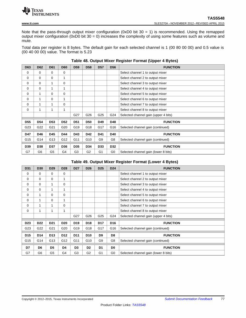
TAS5548www.ti.com SLES270A –NOVEMBER 2012–REVISED APRIL 2015
Note that the pass-through output mixer configuration (0xD0 bit 30 = 1) is recommended. Using the remappedoutput mixer configuration (0xD0 bit 30 = 0) increases the complexity of using some features such as volume andmute.
Total data per register is 8 bytes. The default gain for each selected channel is 1 (00 80 00 00) and 0.5 value is(00 40 00 00) value. The format is 5.23
Table 48. Output Mixer Register Format (Upper 4 Bytes)D63 D62 D61 D60 D59 D58 D57 D56 FUNCTION
0 0 0 0 Select channel 1 to output mixer0 0 0 1 Select channel 2 to output mixer0 0 1 0 Select channel 3 to output mixer0 0 1 1 Select channel 4 to output mixer0 1 0 0 Select channel 5 to output mixer0 1 0 1 Select channel 6 to output mixer0 1 1 0 Select channel 7 to output mixer0 1 1 1 Select channel 8 to output mixer
G27 G26 G25 G24 Selected channel gain (upper 4 bits)
D55 D54 D53 D52 D51 D50 D49 D48 FUNCTIONG23 G22 G21 G20 G19 G18 G17 G16 Selected channel gain (continued)
D47 D46 D45 D44 D43 D42 D41 D40 FUNCTIONG15 G14 G13 G12 G11 G10 G9 G8 Selected channel gain (continued)
D39 D38 D37 D36 D35 D34 D33 D32 FUNCTIONG7 G6 G5 G4 G3 G2 G1 G0 Selected channel gain (lower 8 bits)
Table 49. Output Mixer Register Format (Lower 4 Bytes)D31 D30 D29 D28 D27 D26 D25 D24 FUNCTION
0 0 0 0 Select channel 1 to output mixer0 0 0 1 Select channel 2 to output mixer0 0 1 0 Select channel 3 to output mixer0 0 1 1 Select channel 4 to output mixer0 1 0 0 Select channel 5 to output mixer0 1 0 1 Select channel 6 to output mixer0 1 1 0 Select channel 7 to output mixer0 1 1 1 Select channel 8 to output mixer
G27 G26 G25 G24 Selected channel gain (upper 4 bits)
D23 D22 D21 D20 D19 D18 D17 D16 FUNCTIONG23 G22 G21 G20 G19 G18 G17 G16 Selected channel gain (continued)
D15 D14 D13 D12 D11 D10 D9 D8 FUNCTIONG15 G14 G13 G12 G11 G10 G9 G8 Selected channel gain (continued)
D7 D6 D5 D4 D3 D2 D1 D0 FUNCTIONG7 G6 G5 G4 G3 G2 G1 G0 Selected channel gain (lower 8 bits)
Copyright © 2012–2015, Texas Instruments Incorporated Submit Documentation Feedback 77
Product Folder Links: TAS5548
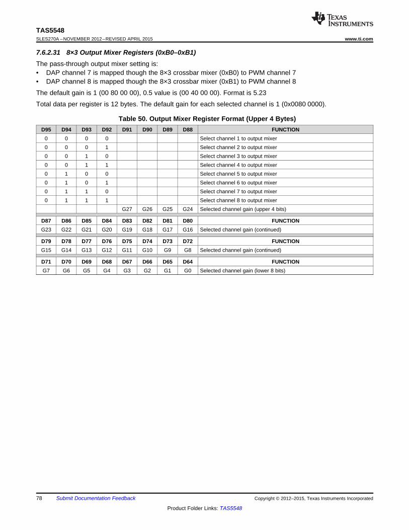
TAS5548SLES270A –NOVEMBER 2012–REVISED APRIL 2015 www.ti.com
7.6.2.31 8×3 Output Mixer Registers (0xB0–0xB1)The pass-through output mixer setting is:• DAP channel 7 is mapped though the 8×3 crossbar mixer (0xB0) to PWM channel 7• DAP channel 8 is mapped though the 8×3 crossbar mixer (0xB1) to PWM channel 8
The default gain is 1 (00 80 00 00), 0.5 value is (00 40 00 00). Format is 5.23
Total data per register is 12 bytes. The default gain for each selected channel is 1 (0x0080 0000).
Table 50. Output Mixer Register Format (Upper 4 Bytes)D95 D94 D93 D92 D91 D90 D89 D88 FUNCTION
0 0 0 0 Select channel 1 to output mixer0 0 0 1 Select channel 2 to output mixer0 0 1 0 Select channel 3 to output mixer0 0 1 1 Select channel 4 to output mixer0 1 0 0 Select channel 5 to output mixer0 1 0 1 Select channel 6 to output mixer0 1 1 0 Select channel 7 to output mixer0 1 1 1 Select channel 8 to output mixer
G27 G26 G25 G24 Selected channel gain (upper 4 bits)
D87 D86 D85 D84 D83 D82 D81 D80 FUNCTIONG23 G22 G21 G20 G19 G18 G17 G16 Selected channel gain (continued)
D79 D78 D77 D76 D75 D74 D73 D72 FUNCTIONG15 G14 G13 G12 G11 G10 G9 G8 Selected channel gain (continued)
D71 D70 D69 D68 D67 D66 D65 D64 FUNCTIONG7 G6 G5 G4 G3 G2 G1 G0 Selected channel gain (lower 8 bits)
78 Submit Documentation Feedback Copyright © 2012–2015, Texas Instruments Incorporated
Product Folder Links: TAS5548
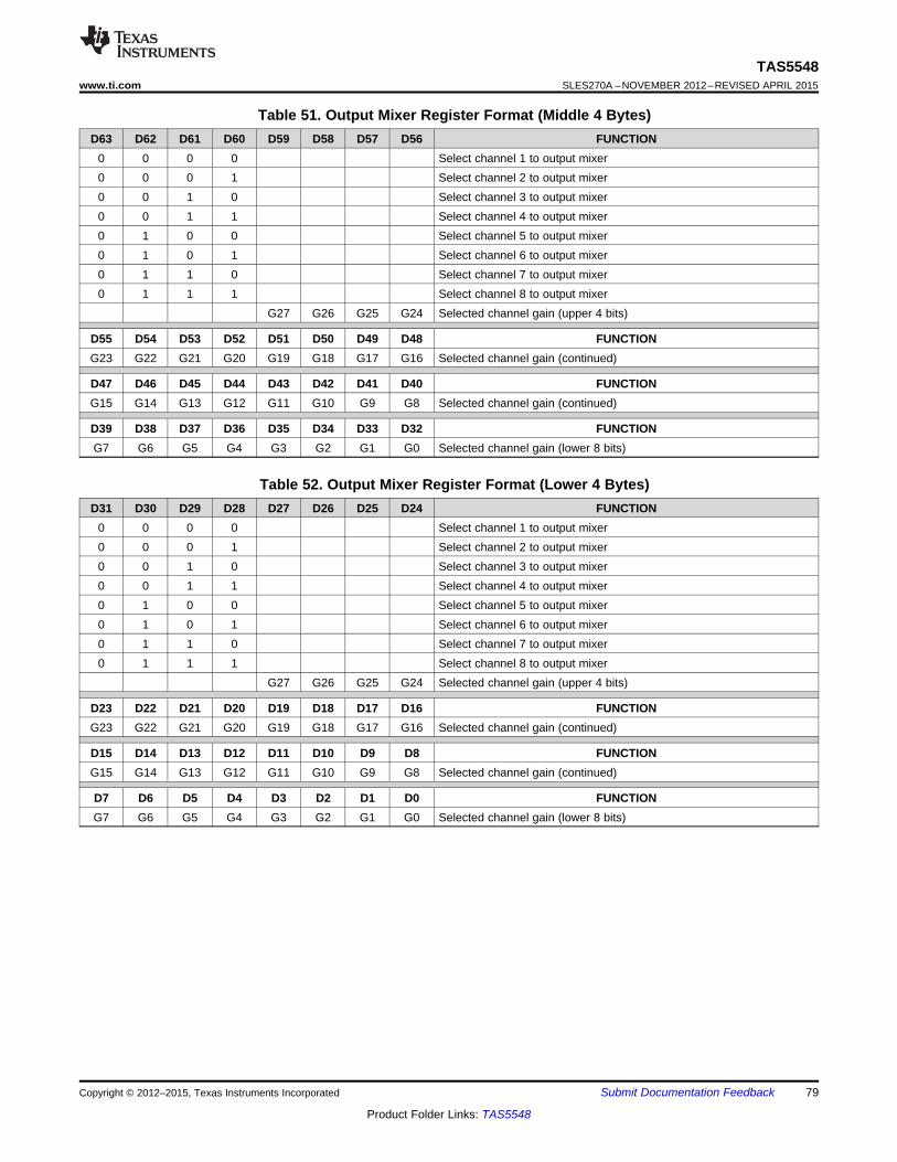
TAS5548www.ti.com SLES270A –NOVEMBER 2012–REVISED APRIL 2015
Table 51. Output Mixer Register Format (Middle 4 Bytes)D63 D62 D61 D60 D59 D58 D57 D56 FUNCTION
0 0 0 0 Select channel 1 to output mixer0 0 0 1 Select channel 2 to output mixer0 0 1 0 Select channel 3 to output mixer0 0 1 1 Select channel 4 to output mixer0 1 0 0 Select channel 5 to output mixer0 1 0 1 Select channel 6 to output mixer0 1 1 0 Select channel 7 to output mixer0 1 1 1 Select channel 8 to output mixer
G27 G26 G25 G24 Selected channel gain (upper 4 bits)
D55 D54 D53 D52 D51 D50 D49 D48 FUNCTIONG23 G22 G21 G20 G19 G18 G17 G16 Selected channel gain (continued)
D47 D46 D45 D44 D43 D42 D41 D40 FUNCTIONG15 G14 G13 G12 G11 G10 G9 G8 Selected channel gain (continued)
D39 D38 D37 D36 D35 D34 D33 D32 FUNCTIONG7 G6 G5 G4 G3 G2 G1 G0 Selected channel gain (lower 8 bits)
Table 52. Output Mixer Register Format (Lower 4 Bytes)D31 D30 D29 D28 D27 D26 D25 D24 FUNCTION
0 0 0 0 Select channel 1 to output mixer0 0 0 1 Select channel 2 to output mixer0 0 1 0 Select channel 3 to output mixer0 0 1 1 Select channel 4 to output mixer0 1 0 0 Select channel 5 to output mixer0 1 0 1 Select channel 6 to output mixer0 1 1 0 Select channel 7 to output mixer0 1 1 1 Select channel 8 to output mixer
G27 G26 G25 G24 Selected channel gain (upper 4 bits)
D23 D22 D21 D20 D19 D18 D17 D16 FUNCTIONG23 G22 G21 G20 G19 G18 G17 G16 Selected channel gain (continued)
D15 D14 D13 D12 D11 D10 D9 D8 FUNCTIONG15 G14 G13 G12 G11 G10 G9 G8 Selected channel gain (continued)
D7 D6 D5 D4 D3 D2 D1 D0 FUNCTIONG7 G6 G5 G4 G3 G2 G1 G0 Selected channel gain (lower 8 bits)
Copyright © 2012–2015, Texas Instruments Incorporated Submit Documentation Feedback 79
Product Folder Links: TAS5548
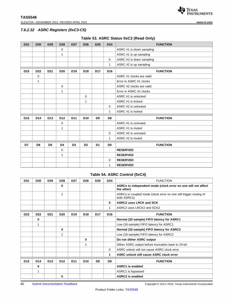
TAS5548SLES270A –NOVEMBER 2012–REVISED APRIL 2015 www.ti.com
7.6.2.32 ASRC Registers (0xC3-C5)
Table 53. ASRC Status 0xC3 (Read Only)D31 D30 D29 D28 D27 D26 D25 D24 FUNCTION
0 ASRC #1 is down sampling1 ASRC #1 is up sampling
0 ASRC #2 is down sampling1 ASRC #2 is up sampling
D23 D22 D21 D20 D19 D18 D17 D16 FUNCTION0 ASRC #1 clocks are valid1 Error in ASRC #1 clocks
0 ASRC #2 clocks are valid1 Error in ASRC #2 clocks
0 ASRC #1 is unlocked1 ASRC #1 is locked
0 ASRC #2 is unlocked1 ASRC #1 is locked
D15 D14 D13 D12 D11 D10 D9 D8 FUNCTION0 ASRC #1 is unmuted1 ASRC #1 is muted
0 ASRC #2 is unmuted1 ASRC #2 is muted
D7 D6 D5 D4 D3 D2 D1 D0 FUNCTION0 RESERVED1 RESERVED
0 RESERVED1 RESERVED
Table 54. ASRC Control (0xC4)D31 D30 D29 D28 D27 D26 D25 D24 FUNCTION
0 ASRCs in independent mode (clock error on one will not affectthe other)
1 ASRCs in coupled mode (clock error on one will trigger muting ofboth ASRCs)
0 ASRC2 uses LRCK and SCK1 ASRC2 uses LRCK2 and SCK2
D23 D22 D21 D20 D19 D18 D17 D16 FUNCTION0 Normal (32-sample) FIFO latency for ASRC11 Low (16-sample) FIFO latency for ASRC1
0 Normal (32-sample) FIFO latency for ASRC21 Low (16-sample) FIFO latency for ASRC2
0 Do not dither ASRC output1 Dither ASRC output before truncation back to 24-bit
0 ASRC unlock will not cause ASRC clock error1 ASRC unlock will cause ASRC clock error
D15 D14 D13 D12 D11 D10 D9 D8 FUNCTION0 ASRC1 is enabled1 ASRC1 is bypassed
0 ASRC2 is enabled
80 Submit Documentation Feedback Copyright © 2012–2015, Texas Instruments Incorporated
Product Folder Links: TAS5548
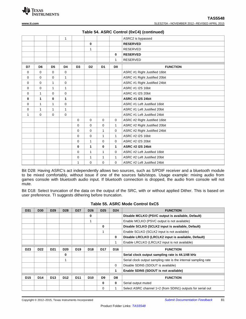
TAS5548www.ti.com SLES270A –NOVEMBER 2012–REVISED APRIL 2015
Table 54. ASRC Control (0xC4) (continued)1 ASRC2 is bypassed
0 RESERVED1 RESERVED
0 RESERVED1 RESERVED
D7 D6 D5 D4 D3 D2 D1 D0 FUNCTION0 0 0 0 ASRC #1 Right Justified 16bit0 0 0 1 ASRC #1 Right Justified 20bit0 0 1 0 ASRC #1 Right Justified 24bit0 0 1 1 ASRC #1 I2S 16bit0 1 0 0 ASRC #1 I2S 20bit0 1 0 1 ASRC #1 I2S 24bit0 1 1 0 ASRC #1 Left Justified 16bit0 1 1 1 ASRC #1 Left Justified 20bit1 0 0 0 ASRC #1 Left Justified 24bit
0 0 0 0 ASRC #2 Right Justified 16bit0 0 0 1 ASRC #2 Right Justified 20bit0 0 1 0 ASRC #2 Right Justified 24bit0 0 1 1 ASRC #2 I2S 16bit0 1 0 0 ASRC #2 I2S 20bit0 1 0 1 ASRC #2 I2S 24bit0 1 1 0 ASRC #2 Left Justified 16bit0 1 1 1 ASRC #2 Left Justified 20bit1 0 0 0 ASRC #2 Left Justified 24bit
Bit D28: Having ASRC's act independently allows two sources, such as S/PDIF receiver and a bluetooth moduleto be mixed comfortably, without issue if one of the sources fails/stops. Usage example: mixing audio fromgames console with bluetooth audio input. If bluetooth connection is dropped, the audio from console will notmute.
Bit D18: Select truncation of the data on the output of the SRC, with or without applied Dither. This is based onuser preference. TI suggests dithering before truncation.
Table 55. ASRC Mode Control 0xC5D31 D30 D29 D28 D27 D26 D25 D24 FUNCTION
0 Disable MCLKO (PSVC output is available, Default)1 Enable MCLKO (PSVC output is not available)
0 Disable SCLKO (SCLK2 input is available, Default)1 Enable SCLKO (SCLK2 input is not available)
0 Disable LRCLKO (LRCLK2 input is available, Default)1 Enable LRCLKO (LRCLK2 input is not available)
D23 D22 D21 D20 D19 D18 D17 D16 FUNCTION0 Serial clock output sampling rate is 44.1/48 kHz1 Serial clock output sampling rate is the internal sampling rate
0 Disable SDIN5 (SDOUT is available)1 Enable SDIN5 (SDOUT is not available)
D15 D14 D13 D12 D11 D10 D9 D8 FUNCTION0 0 Serial output muted0 1 Select ASRC channel 1+2 (from SDIN1) outputs for serial out
Copyright © 2012–2015, Texas Instruments Incorporated Submit Documentation Feedback 81
Product Folder Links: TAS5548
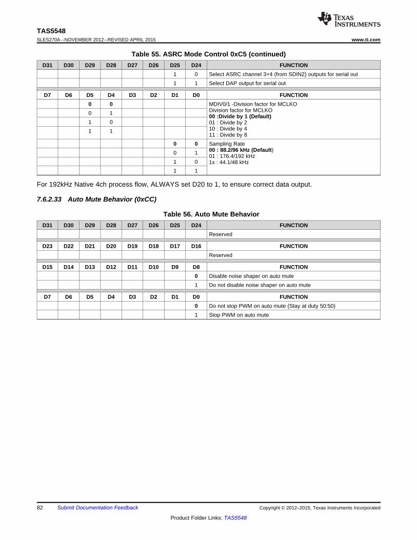
TAS5548SLES270A –NOVEMBER 2012–REVISED APRIL 2015 www.ti.com
Table 55. ASRC Mode Control 0xC5 (continued)D31 D30 D29 D28 D27 D26 D25 D24 FUNCTION
1 0 Select ASRC channel 3+4 (from SDIN2) outputs for serial out1 1 Select DAP output for serial out
D7 D6 D5 D4 D3 D2 D1 D0 FUNCTION0 0 MDIV0/1 -Division factor for MCLKO
Division factor for MCLKO0 1 00 :Divide by 1 (Default)1 0 01 : Divide by 2
10 : Divide by 41 111 : Divide by 8
0 0 Sampling Rate00 : 88.2/96 kHz (Default)0 1 01 : 176.4/192 kHz
1 0 1x : 44.1/48 kHz1 1
For 192kHz Native 4ch process flow, ALWAYS set D20 to 1, to ensure correct data output.
7.6.2.33 Auto Mute Behavior (0xCC)
Table 56. Auto Mute BehaviorD31 D30 D29 D28 D27 D26 D25 D24 FUNCTION
Reserved
D23 D22 D21 D20 D19 D18 D17 D16 FUNCTIONReserved
D15 D14 D13 D12 D11 D10 D9 D8 FUNCTION0 Disable noise shaper on auto mute1 Do not disable noise shaper on auto mute
D7 D6 D5 D4 D3 D2 D1 D0 FUNCTION0 Do not stop PWM on auto mute (Stay at duty 50:50)1 Stop PWM on auto mute
82 Submit Documentation Feedback Copyright © 2012–2015, Texas Instruments Incorporated
Product Folder Links: TAS5548
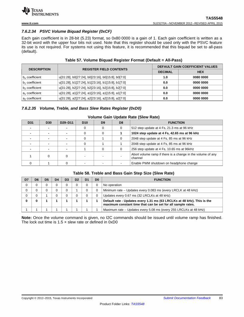
TAS5548www.ti.com SLES270A –NOVEMBER 2012–REVISED APRIL 2015
7.6.2.34 PSVC Volume Biquad Register (0xCF)Each gain coefficient is in 28-bit (5.23) format, so 0x80 0000 is a gain of 1. Each gain coefficient is written as a32-bit word with the upper four bits not used. Note that this register should be used only with the PSVC featureits use is not required. For systems not using this feature, it is recommended that this biquad be set to all-pass(default).
Table 57. Volume Biquad Register Format (Default = All-Pass)DEFAULT GAIN COEFFICIENT VALUES
DESCRIPTION REGISTER FIELD CONTENTSDECIMAL HEX
bo coefficient u[31:28], b0[27:24], b0[23:16], b0[15:8], b0[7:0] 1.0 0080 0000b1 coefficient u[31:28], b1[27:24], b1[23:16], b1[15:8], b1[7:0] 0.0 0000 0000b2 coefficient u[31:28], b2[27:24], b2[23:16], b2[15:8], b2[7:0] 0.0 0000 0000a1 coefficient u[31:28], a1[27:24], a1[23:16], a1[15:8], a1[7:0] 0.0 0000 0000a2 coefficient u[31:28], a2[27:24], a2[23:16], a2[15:8], a2[7:0] 0.0 0000 0000
7.6.2.35 Volume, Treble, and Bass Slew Rates Register (0xD0)
Volume Gain Update Rate (Slew Rate)D31 D30 D29–D11 D10 D9 D8 FUNCTION
- - - 0 0 0 512 step update at 4 Fs, 21.3 ms at 96 kHz- - - 0 0 1 1024 step update at 4 Fs, 42.65 ms at 96 kHz- - - 0 1 0 2048 step update at 4 Fs, 85 ms at 96 kHz- - - 0 1 1 2048 step update at 4 Fs, 85 ms at 96 kHz- - - 1 0 0 256 step update at 4 Fs, 10.65 ms at 96kHz
Abort volume ramp if there is a change in the volume of any1 0 0 - - - channel0 1 0 - - - Enable PWM shutdown on headphone change
Table 58. Treble and Bass Gain Step Size (Slew Rate)D7 D6 D5 D4 D3 D2 D1 D0 FUNCTION0 0 0 0 0 0 0 0 No operation0 0 0 0 0 1 0 0 Minimum rate – Updates every 0.083 ms (every LRCLK at 48 kHz)0 0 1 0 0 0 0 0 Updates every 0.67 ms (32 LRCLKs at 48 kHz)0 0 1 1 1 1 1 1 Default rate - Updates every 1.31 ms (63 LRCLKs at 48 kHz). This is the
maximum constant time that can be set for all sample rates.1 1 1 1 1 1 1 1 Maximum rate – Updates every 5.08 ms (every 255 LRCLKs at 48 kHz)
Note: Once the volume command is given, no I2C commands should be issued until volume ramp has finished.The lock out time is 1.5 × slew rate or defined in 0xD0
Copyright © 2012–2015, Texas Instruments Incorporated Submit Documentation Feedback 83
Product Folder Links: TAS5548
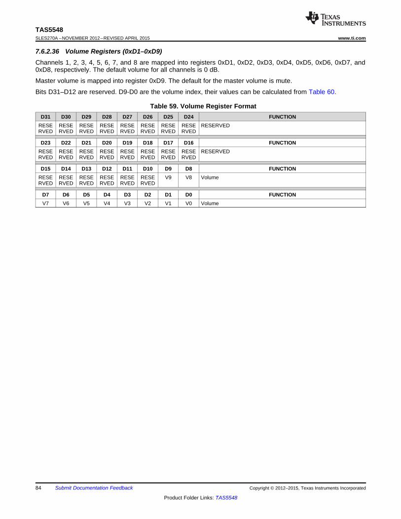
TAS5548SLES270A –NOVEMBER 2012–REVISED APRIL 2015 www.ti.com
7.6.2.36 Volume Registers (0xD1–0xD9)Channels 1, 2, 3, 4, 5, 6, 7, and 8 are mapped into registers 0xD1, 0xD2, 0xD3, 0xD4, 0xD5, 0xD6, 0xD7, and0xD8, respectively. The default volume for all channels is 0 dB.
Master volume is mapped into register 0xD9. The default for the master volume is mute.
Bits D31–D12 are reserved. D9-D0 are the volume index, their values can be calculated from Table 60.
Table 59. Volume Register FormatD31 D30 D29 D28 D27 D26 D25 D24 FUNCTION
RESE RESE RESE RESE RESE RESE RESE RESE RESERVEDRVED RVED RVED RVED RVED RVED RVED RVED
D23 D22 D21 D20 D19 D18 D17 D16 FUNCTIONRESE RESE RESE RESE RESE RESE RESE RESE RESERVEDRVED RVED RVED RVED RVED RVED RVED RVED
D15 D14 D13 D12 D11 D10 D9 D8 FUNCTIONRESE RESE RESE RESE RESE RESE V9 V8 VolumeRVED RVED RVED RVED RVED RVED
D7 D6 D5 D4 D3 D2 D1 D0 FUNCTIONV7 V6 V5 V4 V3 V2 V1 V0 Volume
84 Submit Documentation Feedback Copyright © 2012–2015, Texas Instruments Incorporated
Product Folder Links: TAS5548
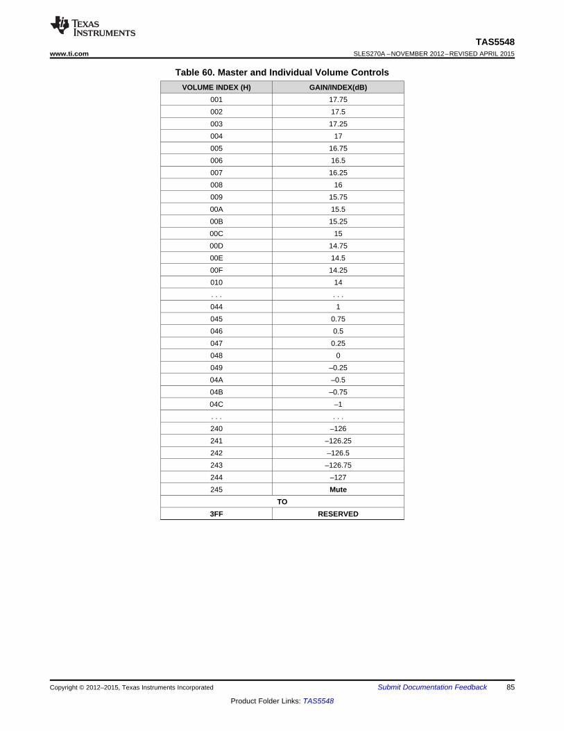
TAS5548www.ti.com SLES270A –NOVEMBER 2012–REVISED APRIL 2015
Table 60. Master and Individual Volume ControlsVOLUME INDEX (H) GAIN/INDEX(dB)
001 17.75002 17.5003 17.25004 17005 16.75006 16.5007 16.25008 16009 15.7500A 15.500B 15.2500C 1500D 14.7500E 14.500F 14.25010 14. . . . . .044 1045 0.75046 0.5047 0.25048 0049 –0.2504A –0.504B –0.7504C –1. . . . . .240 –126241 –126.25242 –126.5243 –126.75244 –127245 Mute
TO3FF RESERVED
Copyright © 2012–2015, Texas Instruments Incorporated Submit Documentation Feedback 85
Product Folder Links: TAS5548
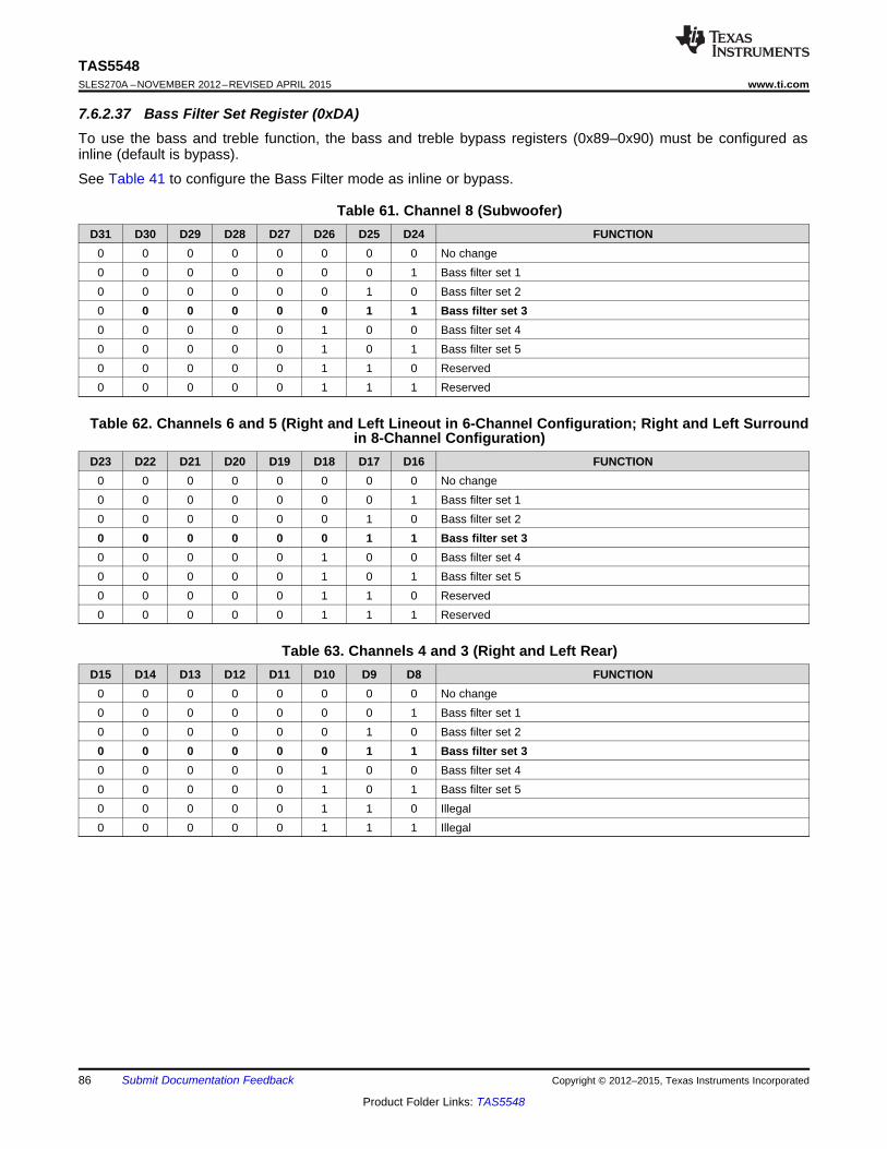
TAS5548SLES270A –NOVEMBER 2012–REVISED APRIL 2015 www.ti.com
7.6.2.37 Bass Filter Set Register (0xDA)To use the bass and treble function, the bass and treble bypass registers (0x89–0x90) must be configured asinline (default is bypass).
See Table 41 to configure the Bass Filter mode as inline or bypass.
Table 61. Channel 8 (Subwoofer)D31 D30 D29 D28 D27 D26 D25 D24 FUNCTION
0 0 0 0 0 0 0 0 No change0 0 0 0 0 0 0 1 Bass filter set 10 0 0 0 0 0 1 0 Bass filter set 20 0 0 0 0 0 1 1 Bass filter set 30 0 0 0 0 1 0 0 Bass filter set 40 0 0 0 0 1 0 1 Bass filter set 50 0 0 0 0 1 1 0 Reserved0 0 0 0 0 1 1 1 Reserved
Table 62. Channels 6 and 5 (Right and Left Lineout in 6-Channel Configuration; Right and Left Surroundin 8-Channel Configuration)
D23 D22 D21 D20 D19 D18 D17 D16 FUNCTION0 0 0 0 0 0 0 0 No change0 0 0 0 0 0 0 1 Bass filter set 10 0 0 0 0 0 1 0 Bass filter set 20 0 0 0 0 0 1 1 Bass filter set 30 0 0 0 0 1 0 0 Bass filter set 40 0 0 0 0 1 0 1 Bass filter set 50 0 0 0 0 1 1 0 Reserved0 0 0 0 0 1 1 1 Reserved
Table 63. Channels 4 and 3 (Right and Left Rear)D15 D14 D13 D12 D11 D10 D9 D8 FUNCTION
0 0 0 0 0 0 0 0 No change0 0 0 0 0 0 0 1 Bass filter set 10 0 0 0 0 0 1 0 Bass filter set 20 0 0 0 0 0 1 1 Bass filter set 30 0 0 0 0 1 0 0 Bass filter set 40 0 0 0 0 1 0 1 Bass filter set 50 0 0 0 0 1 1 0 Illegal0 0 0 0 0 1 1 1 Illegal
86 Submit Documentation Feedback Copyright © 2012–2015, Texas Instruments Incorporated
Product Folder Links: TAS5548
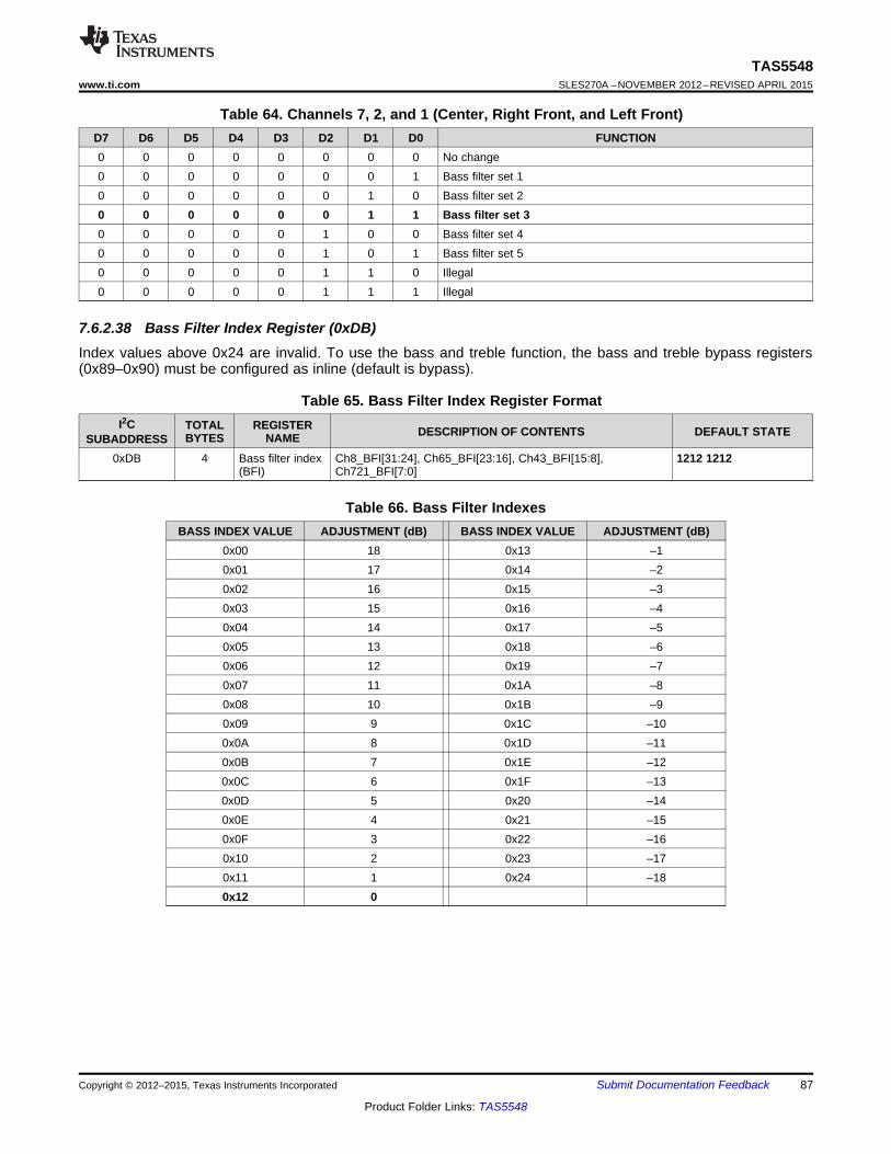
TAS5548www.ti.com SLES270A –NOVEMBER 2012–REVISED APRIL 2015
Table 64. Channels 7, 2, and 1 (Center, Right Front, and Left Front)D7 D6 D5 D4 D3 D2 D1 D0 FUNCTION0 0 0 0 0 0 0 0 No change0 0 0 0 0 0 0 1 Bass filter set 10 0 0 0 0 0 1 0 Bass filter set 20 0 0 0 0 0 1 1 Bass filter set 30 0 0 0 0 1 0 0 Bass filter set 40 0 0 0 0 1 0 1 Bass filter set 50 0 0 0 0 1 1 0 Illegal0 0 0 0 0 1 1 1 Illegal
7.6.2.38 Bass Filter Index Register (0xDB)Index values above 0x24 are invalid. To use the bass and treble function, the bass and treble bypass registers(0x89–0x90) must be configured as inline (default is bypass).
Table 65. Bass Filter Index Register FormatI2C TOTAL REGISTER DESCRIPTION OF CONTENTS DEFAULT STATEBYTES NAMESUBADDRESS
0xDB 4 Bass filter index Ch8_BFI[31:24], Ch65_BFI[23:16], Ch43_BFI[15:8], 1212 1212(BFI) Ch721_BFI[7:0]
Table 66. Bass Filter IndexesBASS INDEX VALUE ADJUSTMENT (dB) BASS INDEX VALUE ADJUSTMENT (dB)
0x00 18 0x13 –10x01 17 0x14 –20x02 16 0x15 –30x03 15 0x16 –40x04 14 0x17 –50x05 13 0x18 –60x06 12 0x19 –70x07 11 0x1A –80x08 10 0x1B –90x09 9 0x1C –100x0A 8 0x1D –110x0B 7 0x1E –120x0C 6 0x1F –130x0D 5 0x20 –140x0E 4 0x21 –150x0F 3 0x22 –160x10 2 0x23 –170x11 1 0x24 –180x12 0
Copyright © 2012–2015, Texas Instruments Incorporated Submit Documentation Feedback 87
Product Folder Links: TAS5548
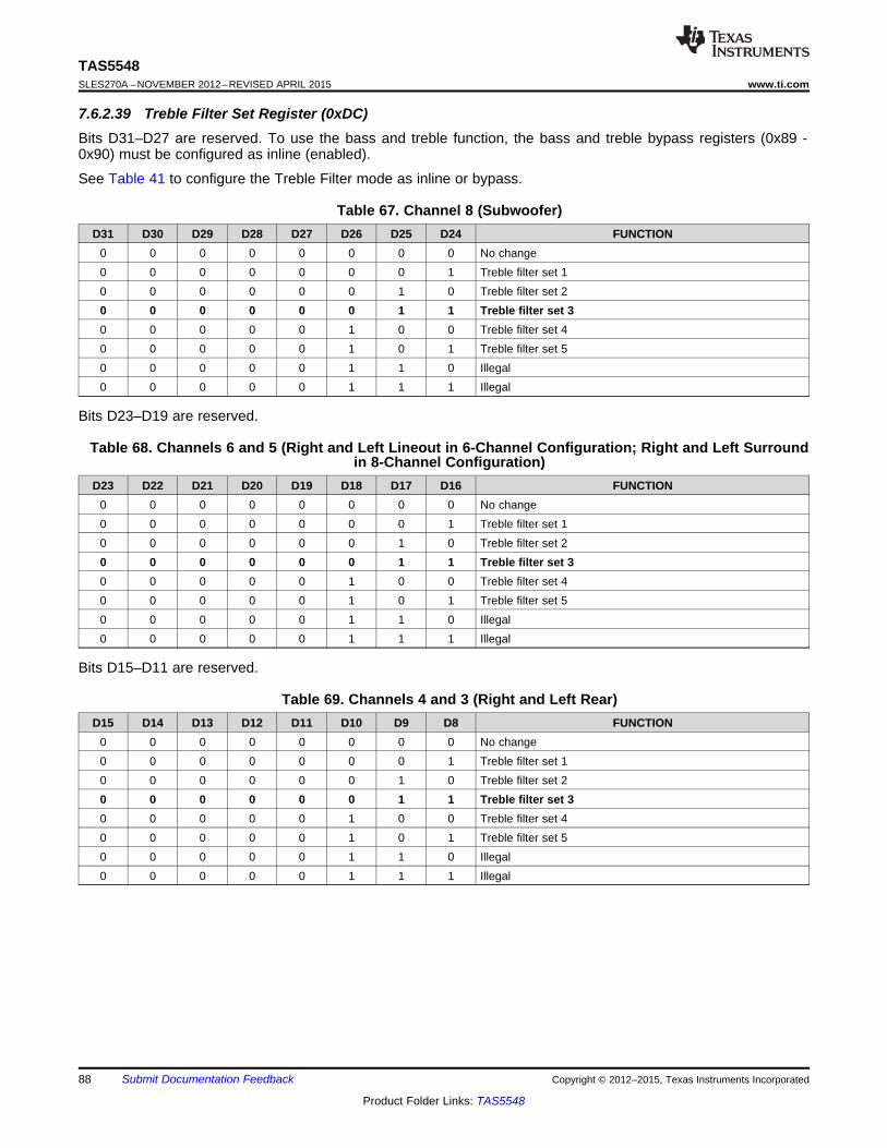
TAS5548SLES270A –NOVEMBER 2012–REVISED APRIL 2015 www.ti.com
7.6.2.39 Treble Filter Set Register (0xDC)Bits D31–D27 are reserved. To use the bass and treble function, the bass and treble bypass registers (0x89 -0x90) must be configured as inline (enabled).
See Table 41 to configure the Treble Filter mode as inline or bypass.
Table 67. Channel 8 (Subwoofer)D31 D30 D29 D28 D27 D26 D25 D24 FUNCTION
0 0 0 0 0 0 0 0 No change0 0 0 0 0 0 0 1 Treble filter set 10 0 0 0 0 0 1 0 Treble filter set 20 0 0 0 0 0 1 1 Treble filter set 30 0 0 0 0 1 0 0 Treble filter set 40 0 0 0 0 1 0 1 Treble filter set 50 0 0 0 0 1 1 0 Illegal0 0 0 0 0 1 1 1 Illegal
Bits D23–D19 are reserved.
Table 68. Channels 6 and 5 (Right and Left Lineout in 6-Channel Configuration; Right and Left Surroundin 8-Channel Configuration)
D23 D22 D21 D20 D19 D18 D17 D16 FUNCTION0 0 0 0 0 0 0 0 No change0 0 0 0 0 0 0 1 Treble filter set 10 0 0 0 0 0 1 0 Treble filter set 20 0 0 0 0 0 1 1 Treble filter set 30 0 0 0 0 1 0 0 Treble filter set 40 0 0 0 0 1 0 1 Treble filter set 50 0 0 0 0 1 1 0 Illegal0 0 0 0 0 1 1 1 Illegal
Bits D15–D11 are reserved.
Table 69. Channels 4 and 3 (Right and Left Rear)D15 D14 D13 D12 D11 D10 D9 D8 FUNCTION
0 0 0 0 0 0 0 0 No change0 0 0 0 0 0 0 1 Treble filter set 10 0 0 0 0 0 1 0 Treble filter set 20 0 0 0 0 0 1 1 Treble filter set 30 0 0 0 0 1 0 0 Treble filter set 40 0 0 0 0 1 0 1 Treble filter set 50 0 0 0 0 1 1 0 Illegal0 0 0 0 0 1 1 1 Illegal
88 Submit Documentation Feedback Copyright © 2012–2015, Texas Instruments Incorporated
Product Folder Links: TAS5548
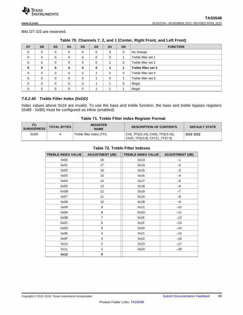
TAS5548www.ti.com SLES270A –NOVEMBER 2012–REVISED APRIL 2015
Bits D7–D3 are reserved.
Table 70. Channels 7, 2, and 1 (Center, Right Front, and Left Front)D7 D6 D5 D4 D3 D2 D1 D0 FUNCTION0 0 0 0 0 0 0 0 No change0 0 0 0 0 0 0 1 Treble filter set 10 0 0 0 0 0 1 0 Treble filter set 20 0 0 0 0 0 1 1 Treble filter set 30 0 0 0 0 1 0 0 Treble filter set 40 0 0 0 0 1 0 1 Treble filter set 50 0 0 0 0 1 1 0 Illegal0 0 0 0 0 1 1 1 Illegal
7.6.2.40 Treble Filter Index (0xDD)Index values above 0x24 are invalid. To use the bass and treble function, the bass and treble bypass registers(0x89 - 0x90) must be configured as inline (enabled).
Table 71. Treble Filter Index Register FormatREGISTERI2C TOTAL BYTES DESCRIPTION OF CONTENTS DEFAULT STATESUBADDRESS NAME
0xDD 4 Treble filter index (TFI) Ch8_TFI[31:24], Ch65_TFI[23:16], 1212 1212Ch43_TFI[15:8], Ch721_TFI[7:0]
Table 72. Treble Filter IndexesTREBLE INDEX VALUE ADJUSTMENT (dB) TREBLE INDEX VALUE ADJUSTMENT (dB)
0x00 18 0x13 –10x01 17 0x14 –20x02 16 0x15 –30x03 15 0x16 –40x04 14 0x17 –50x05 13 0x18 –60x\06 12 0x19 –70x07 11 0x1A –80x08 10 0x1B –90x09 9 0x1C –100x0A 8 0x1D –110x0B 7 0x1E –120x0C 6 0x1F –130x0D 5 0x20 –140x0E 4 0x21 –150x0F 3 0x22 –160x10 2 0x23 –170x11 1 0x24 –180x12 0
Copyright © 2012–2015, Texas Instruments Incorporated Submit Documentation Feedback 89
Product Folder Links: TAS5548
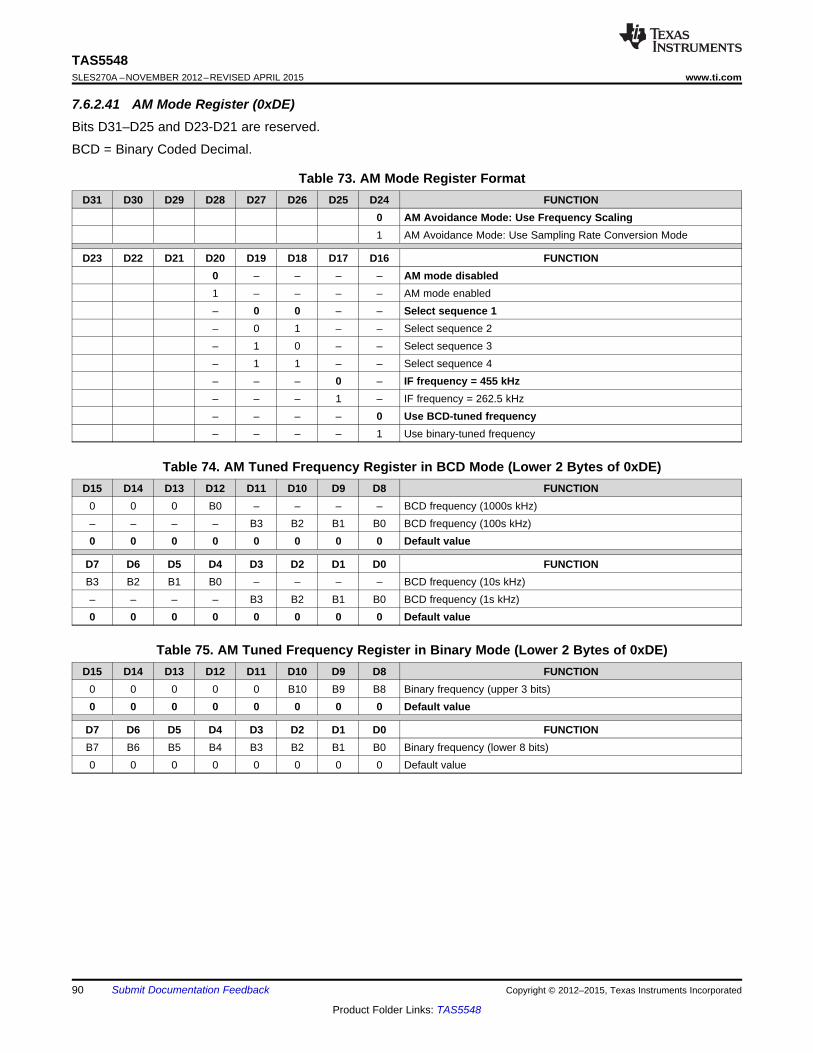
TAS5548SLES270A –NOVEMBER 2012–REVISED APRIL 2015 www.ti.com
7.6.2.41 AM Mode Register (0xDE)Bits D31–D25 and D23-D21 are reserved.
BCD = Binary Coded Decimal.
Table 73. AM Mode Register FormatD31 D30 D29 D28 D27 D26 D25 D24 FUNCTION
0 AM Avoidance Mode: Use Frequency Scaling1 AM Avoidance Mode: Use Sampling Rate Conversion Mode
D23 D22 D21 D20 D19 D18 D17 D16 FUNCTION0 – – – – AM mode disabled1 – – – – AM mode enabled– 0 0 – – Select sequence 1– 0 1 – – Select sequence 2– 1 0 – – Select sequence 3– 1 1 – – Select sequence 4– – – 0 – IF frequency = 455 kHz– – – 1 – IF frequency = 262.5 kHz– – – – 0 Use BCD-tuned frequency– – – – 1 Use binary-tuned frequency
Table 74. AM Tuned Frequency Register in BCD Mode (Lower 2 Bytes of 0xDE)D15 D14 D13 D12 D11 D10 D9 D8 FUNCTION
0 0 0 B0 – – – – BCD frequency (1000s kHz)– – – – B3 B2 B1 B0 BCD frequency (100s kHz)0 0 0 0 0 0 0 0 Default value
D7 D6 D5 D4 D3 D2 D1 D0 FUNCTIONB3 B2 B1 B0 – – – – BCD frequency (10s kHz)– – – – B3 B2 B1 B0 BCD frequency (1s kHz)0 0 0 0 0 0 0 0 Default value
Table 75. AM Tuned Frequency Register in Binary Mode (Lower 2 Bytes of 0xDE)D15 D14 D13 D12 D11 D10 D9 D8 FUNCTION
0 0 0 0 0 B10 B9 B8 Binary frequency (upper 3 bits)0 0 0 0 0 0 0 0 Default value
D7 D6 D5 D4 D3 D2 D1 D0 FUNCTIONB7 B6 B5 B4 B3 B2 B1 B0 Binary frequency (lower 8 bits)0 0 0 0 0 0 0 0 Default value
90 Submit Documentation Feedback Copyright © 2012–2015, Texas Instruments Incorporated
Product Folder Links: TAS5548
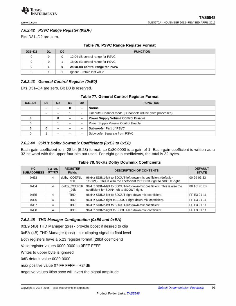
TAS5548www.ti.com SLES270A –NOVEMBER 2012–REVISED APRIL 2015
7.6.2.42 PSVC Range Register (0xDF)Bits D31–D2 are zero.
Table 76. PSVC Range Register FormatD31–D2 D1 D0 FUNCTION
0 0 0 12.04-dB control range for PSVC0 0 1 18.06-dB control range for PSVC0 1 0 24.08-dB control range for PSVC0 1 1 Ignore – retain last value
7.6.2.43 General Control Register (0xE0)Bits D31–D4 are zero. Bit D0 is reserved.
Table 77. General Control Register FormatD31–D4 D3 D2 D1 D0 FUNCTION
– – 0 – Normal– – 1 - Lineout/6 Channel mode (6Channels will be pwm processed)
0 0 – – Power Supply Volume Control Disable0 1 – – Power Supply Volume Control Enable0 0 – – – Subwoofer Part of PSVC0 1 – – – Subwoofer Separate from PSVC
7.6.2.44 96kHz Dolby Downmix Coefficients (0xE3 to 0xE8)Each gain coefficient is in 28-bit (5.23) format, so 0x80 0000 is a gain of 1. Each gain coefficient is written as a32-bit word with the upper four bits not used. For eight gain coefficients, the total is 32 bytes.
Table 78. 96kHz Dolby Downmix CoefficientsI2C REGISTER DEFAULTTOTAL DESCRIPTION OF CONTENTSBYTESSUBADDRESS Fields STATE
0xE3 4 dolby_COEF1L_ 96kHz SDIN1-left to SDOUT-left down-mix coefficient (default = 00 29 03 3396k 1/3.121) . This is also the coefficient for SDIN1-right to SDOUT-right.
0xE4 4 dolby_COEF1R 96kHz SDIN4-left to SDOUT-left down-mix coefficient. This is also the 00 1C FE EF_96k coefficient for SDIN4-left to SDOUT-right.
0xE5 4 TBD 96kHz SDIN2-left to SDOUT-right down-mix coefficient. FF E3 01 110xE6 4 TBD 96kHz SDIN2-right to SDOUT-right down-mix coefficient. FF E3 01 110xE7 4 TBD 96kHz SDIN2-left to SDOUT-left down-mix coefficient. FF E3 01 110xE8 4 TBD 96kHz SDIN2-right to SDOUT-left down-mix coefficient. FF E3 01 11
7.6.2.45 THD Manager Configuration (0xE9 and 0xEA)0xE9 (4B) THD Manager (pre) - provide boost if desired to clip
0xEA (4B) THD Manager (post) - cut clipping signal to final level
Both registers have a 5.23 register format (28bit coefficient)
Valid register values 0000 0000 to 0FFF FFFF
Writes to upper byte is ignored
0dB default value 0080 0000
max positive value 07 FF FFFF = +24dB
negative values 08xx xxxx will invert the signal amplitude
Copyright © 2012–2015, Texas Instruments Incorporated Submit Documentation Feedback 91
Product Folder Links: TAS5548
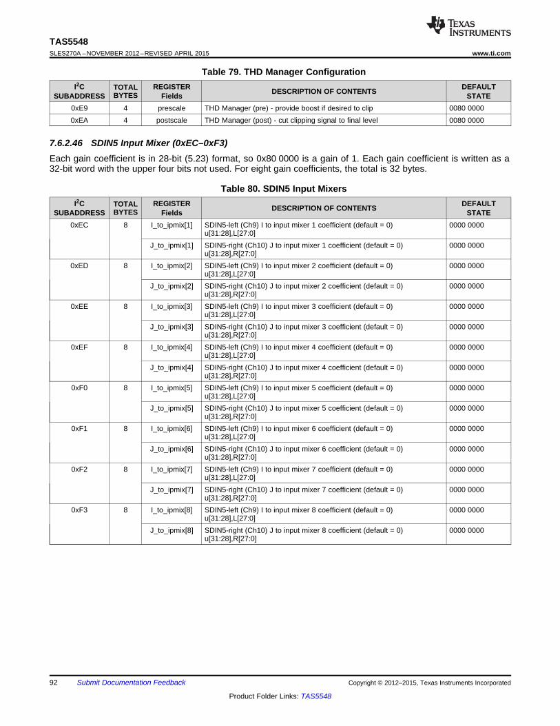
TAS5548SLES270A –NOVEMBER 2012–REVISED APRIL 2015 www.ti.com
Table 79. THD Manager ConfigurationI2C REGISTER DEFAULTTOTAL DESCRIPTION OF CONTENTSBYTESSUBADDRESS Fields STATE
0xE9 4 prescale THD Manager (pre) - provide boost if desired to clip 0080 00000xEA 4 postscale THD Manager (post) - cut clipping signal to final level 0080 0000
7.6.2.46 SDIN5 Input Mixer (0xEC–0xF3)Each gain coefficient is in 28-bit (5.23) format, so 0x80 0000 is a gain of 1. Each gain coefficient is written as a32-bit word with the upper four bits not used. For eight gain coefficients, the total is 32 bytes.
Table 80. SDIN5 Input MixersI2C REGISTER DEFAULTTOTAL DESCRIPTION OF CONTENTSBYTESSUBADDRESS Fields STATE
0xEC 8 I_to_ipmix[1] SDIN5-left (Ch9) I to input mixer 1 coefficient (default = 0) 0000 0000u[31:28],L[27:0]
J_to_ipmix[1] SDIN5-right (Ch10) J to input mixer 1 coefficient (default = 0) 0000 0000u[31:28],R[27:0]
0xED 8 I_to_ipmix[2] SDIN5-left (Ch9) I to input mixer 2 coefficient (default = 0) 0000 0000u[31:28],L[27:0]
J_to_ipmix[2] SDIN5-right (Ch10) J to input mixer 2 coefficient (default = 0) 0000 0000u[31:28],R[27:0]
0xEE 8 I_to_ipmix[3] SDIN5-left (Ch9) I to input mixer 3 coefficient (default = 0) 0000 0000u[31:28],L[27:0]
J_to_ipmix[3] SDIN5-right (Ch10) J to input mixer 3 coefficient (default = 0) 0000 0000u[31:28],R[27:0]
0xEF 8 I_to_ipmix[4] SDIN5-left (Ch9) I to input mixer 4 coefficient (default = 0) 0000 0000u[31:28],L[27:0]
J_to_ipmix[4] SDIN5-right (Ch10) J to input mixer 4 coefficient (default = 0) 0000 0000u[31:28],R[27:0]
0xF0 8 I_to_ipmix[5] SDIN5-left (Ch9) I to input mixer 5 coefficient (default = 0) 0000 0000u[31:28],L[27:0]
J_to_ipmix[5] SDIN5-right (Ch10) J to input mixer 5 coefficient (default = 0) 0000 0000u[31:28],R[27:0]
0xF1 8 I_to_ipmix[6] SDIN5-left (Ch9) I to input mixer 6 coefficient (default = 0) 0000 0000u[31:28],L[27:0]
J_to_ipmix[6] SDIN5-right (Ch10) J to input mixer 6 coefficient (default = 0) 0000 0000u[31:28],R[27:0]
0xF2 8 I_to_ipmix[7] SDIN5-left (Ch9) I to input mixer 7 coefficient (default = 0) 0000 0000u[31:28],L[27:0]
J_to_ipmix[7] SDIN5-right (Ch10) J to input mixer 7 coefficient (default = 0) 0000 0000u[31:28],R[27:0]
0xF3 8 I_to_ipmix[8] SDIN5-left (Ch9) I to input mixer 8 coefficient (default = 0) 0000 0000u[31:28],L[27:0]
J_to_ipmix[8] SDIN5-right (Ch10) J to input mixer 8 coefficient (default = 0) 0000 0000u[31:28],R[27:0]
92 Submit Documentation Feedback Copyright © 2012–2015, Texas Instruments Incorporated
Product Folder Links: TAS5548
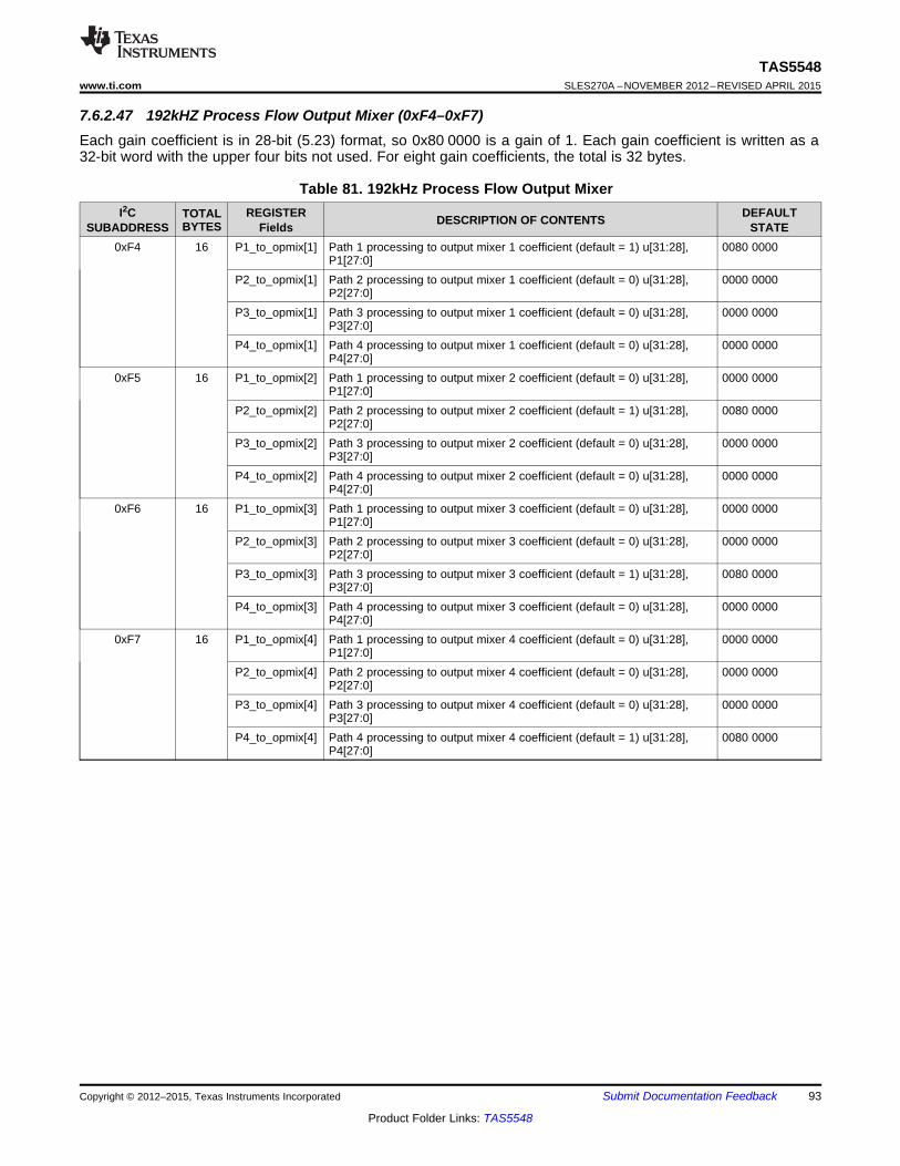
TAS5548www.ti.com SLES270A –NOVEMBER 2012–REVISED APRIL 2015
7.6.2.47 192kHZ Process Flow Output Mixer (0xF4–0xF7)Each gain coefficient is in 28-bit (5.23) format, so 0x80 0000 is a gain of 1. Each gain coefficient is written as a32-bit word with the upper four bits not used. For eight gain coefficients, the total is 32 bytes.
Table 81. 192kHz Process Flow Output MixerI2C REGISTER DEFAULTTOTAL DESCRIPTION OF CONTENTSBYTESSUBADDRESS Fields STATE
0xF4 16 P1_to_opmix[1] Path 1 processing to output mixer 1 coefficient (default = 1) u[31:28], 0080 0000P1[27:0]
P2_to_opmix[1] Path 2 processing to output mixer 1 coefficient (default = 0) u[31:28], 0000 0000P2[27:0]
P3_to_opmix[1] Path 3 processing to output mixer 1 coefficient (default = 0) u[31:28], 0000 0000P3[27:0]
P4_to_opmix[1] Path 4 processing to output mixer 1 coefficient (default = 0) u[31:28], 0000 0000P4[27:0]
0xF5 16 P1_to_opmix[2] Path 1 processing to output mixer 2 coefficient (default = 0) u[31:28], 0000 0000P1[27:0]
P2_to_opmix[2] Path 2 processing to output mixer 2 coefficient (default = 1) u[31:28], 0080 0000P2[27:0]
P3_to_opmix[2] Path 3 processing to output mixer 2 coefficient (default = 0) u[31:28], 0000 0000P3[27:0]
P4_to_opmix[2] Path 4 processing to output mixer 2 coefficient (default = 0) u[31:28], 0000 0000P4[27:0]
0xF6 16 P1_to_opmix[3] Path 1 processing to output mixer 3 coefficient (default = 0) u[31:28], 0000 0000P1[27:0]
P2_to_opmix[3] Path 2 processing to output mixer 3 coefficient (default = 0) u[31:28], 0000 0000P2[27:0]
P3_to_opmix[3] Path 3 processing to output mixer 3 coefficient (default = 1) u[31:28], 0080 0000P3[27:0]
P4_to_opmix[3] Path 4 processing to output mixer 3 coefficient (default = 0) u[31:28], 0000 0000P4[27:0]
0xF7 16 P1_to_opmix[4] Path 1 processing to output mixer 4 coefficient (default = 0) u[31:28], 0000 0000P1[27:0]
P2_to_opmix[4] Path 2 processing to output mixer 4 coefficient (default = 0) u[31:28], 0000 0000P2[27:0]
P3_to_opmix[4] Path 3 processing to output mixer 4 coefficient (default = 0) u[31:28], 0000 0000P3[27:0]
P4_to_opmix[4] Path 4 processing to output mixer 4 coefficient (default = 1) u[31:28], 0080 0000P4[27:0]
Copyright © 2012–2015, Texas Instruments Incorporated Submit Documentation Feedback 93
Product Folder Links: TAS5548
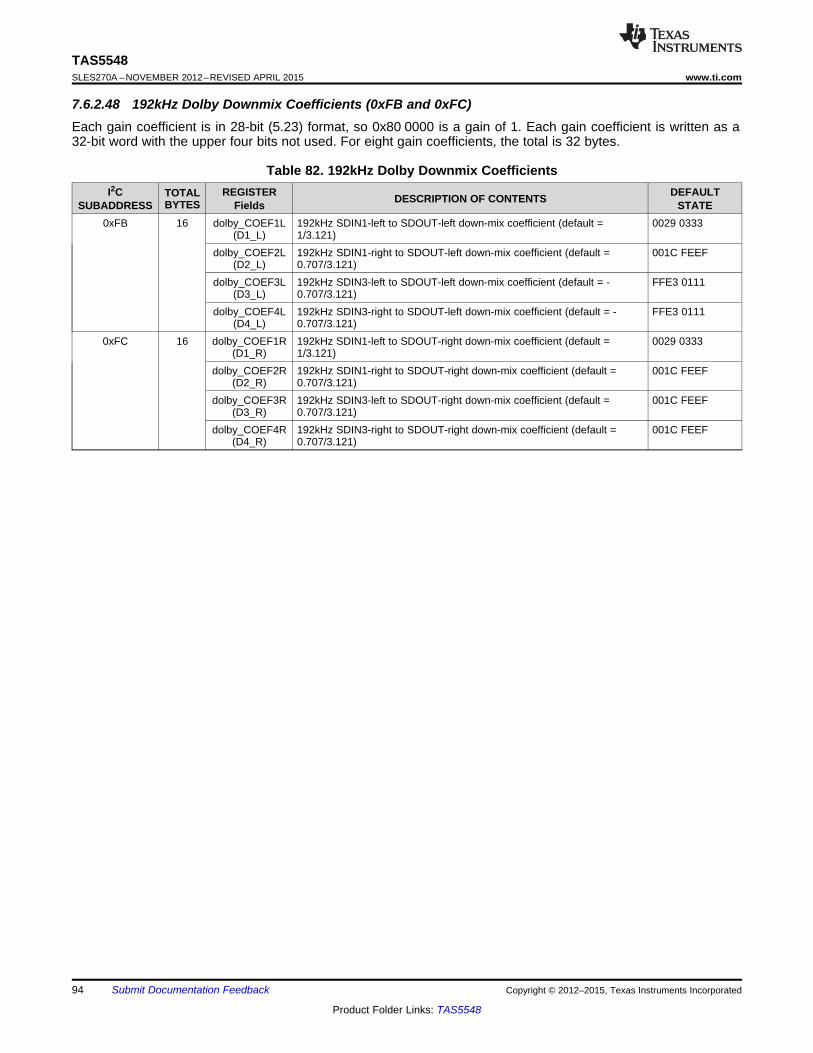
TAS5548SLES270A –NOVEMBER 2012–REVISED APRIL 2015 www.ti.com
7.6.2.48 192kHz Dolby Downmix Coefficients (0xFB and 0xFC)Each gain coefficient is in 28-bit (5.23) format, so 0x80 0000 is a gain of 1. Each gain coefficient is written as a32-bit word with the upper four bits not used. For eight gain coefficients, the total is 32 bytes.
Table 82. 192kHz Dolby Downmix CoefficientsI2C REGISTER DEFAULTTOTAL DESCRIPTION OF CONTENTSBYTESSUBADDRESS Fields STATE
0xFB 16 dolby_COEF1L 192kHz SDIN1-left to SDOUT-left down-mix coefficient (default = 0029 0333(D1_L) 1/3.121)
dolby_COEF2L 192kHz SDIN1-right to SDOUT-left down-mix coefficient (default = 001C FEEF(D2_L) 0.707/3.121)
dolby_COEF3L 192kHz SDIN3-left to SDOUT-left down-mix coefficient (default = - FFE3 0111(D3_L) 0.707/3.121)
dolby_COEF4L 192kHz SDIN3-right to SDOUT-left down-mix coefficient (default = - FFE3 0111(D4_L) 0.707/3.121)
0xFC 16 dolby_COEF1R 192kHz SDIN1-left to SDOUT-right down-mix coefficient (default = 0029 0333(D1_R) 1/3.121)
dolby_COEF2R 192kHz SDIN1-right to SDOUT-right down-mix coefficient (default = 001C FEEF(D2_R) 0.707/3.121)
dolby_COEF3R 192kHz SDIN3-left to SDOUT-right down-mix coefficient (default = 001C FEEF(D3_R) 0.707/3.121)
dolby_COEF4R 192kHz SDIN3-right to SDOUT-right down-mix coefficient (default = 001C FEEF(D4_R) 0.707/3.121)
spacer
94 Submit Documentation Feedback Copyright © 2012–2015, Texas Instruments Incorporated
Product Folder Links: TAS5548
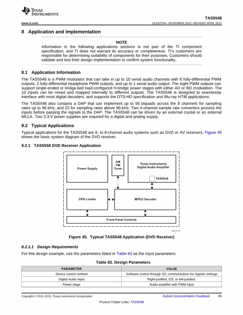
TAS55x8
DVD Loader
Power Supply
Texas InstrumentsDigital Audio Amplifier
MPEG Decoder
Front-Panel Controls
AMFM
Tuner
B0012-03
TAS5548www.ti.com SLES270A –NOVEMBER 2012–REVISED APRIL 2015
8 Application and Implementation
NOTEInformation in the following applications sections is not part of the TI componentspecification, and TI does not warrant its accuracy or completeness. TI’s customers areresponsible for determining suitability of components for their purposes. Customers shouldvalidate and test their design implementation to confirm system functionality.
8.1 Application InformationThe TAS5548 is a PWM modulator that can take in up to 10 serial audio channels with 8 fully-differential PWMoutputs, 2 fully-differential headphone PWM outputs, and up to 1 serial audio output. The eight PWM outputs cansupport single-ended or bridge-tied load-configured H-bridge power stages with either AD or BD modulation. The10 inputs can be mixed and mapped internally to different outputs. The TAS5548 is designed to seamlesslyinterface with most digital decoders, and supports the DTS-HD specification and Blu-ray HTiB applications.
The TAS5548 also contains a DAP that can implement up to 56 biquads across the 8 channels for samplingrates up to 96-kHz, and 22 for sampling rates above 96-kHz. Two 4-channel sample rate converters process theinputs before passing the signals to the DAP. The TAS5548 can be driven by an external crystal or an externalMCLK. Two 3.3-V power supplies are required for a digital and analog supply.
8.2 Typical ApplicationsTypical applications for the TAS5548 are 6- to 8-channel audio systems such as DVD or AV receivers. Figure 45shows the basic system diagram of the DVD receiver.
8.2.1 TAS5558 DVD Receiver Application
Figure 45. Typical TAS5548 Application (DVD Receiver)
8.2.1.1 Design RequirementsFor this design example, use the parameters listed in Table 83 as the input parameters.
Table 83. Design ParametersPARAMETER VALUE
Device control method Software control through I2C communication for register settingsDigital Audio input Right-justified, I2S, or left-justified.
Power stage Audio amplifier with PWM input
Copyright © 2012–2015, Texas Instruments Incorporated Submit Documentation Feedback 95
Product Folder Links: TAS5548
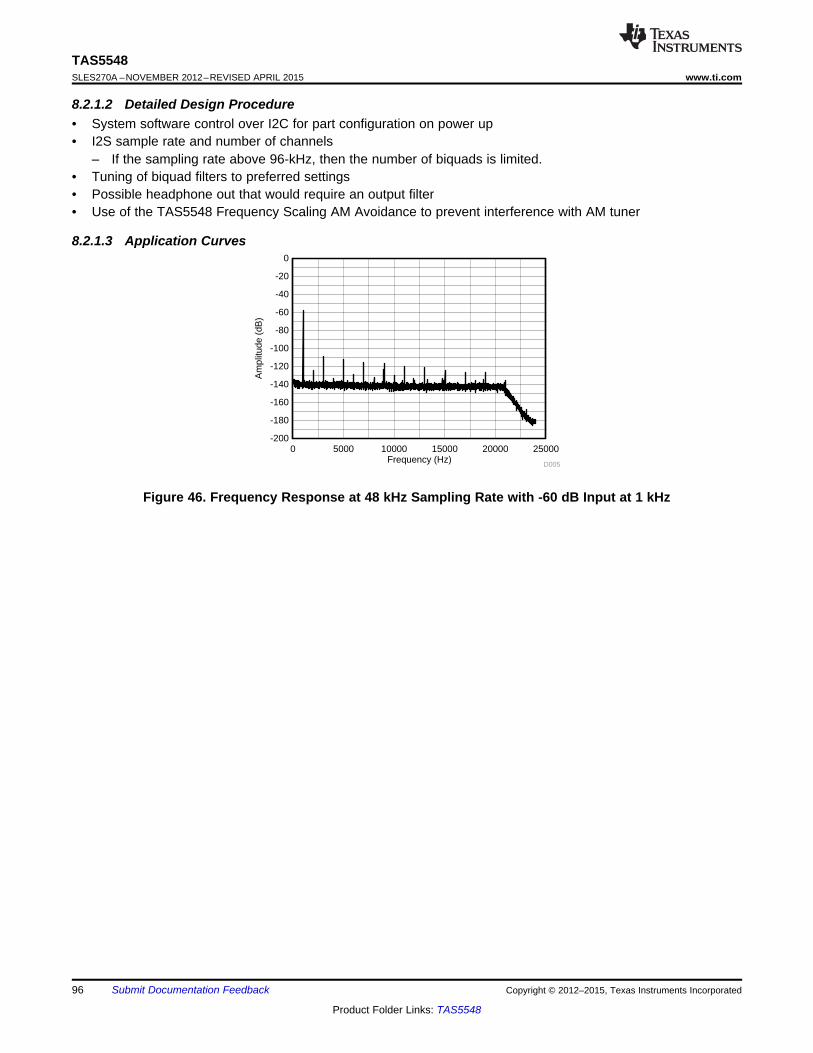
Frequency (Hz)
Am
plitu
de (
dB)
0 5000 10000 15000 20000 25000-200
-180
-160
-140
-120
-100
-80
-60
-40
-20
0
D005
TAS5548SLES270A –NOVEMBER 2012–REVISED APRIL 2015 www.ti.com
8.2.1.2 Detailed Design Procedure• System software control over I2C for part configuration on power up• I2S sample rate and number of channels
– If the sampling rate above 96-kHz, then the number of biquads is limited.• Tuning of biquad filters to preferred settings• Possible headphone out that would require an output filter• Use of the TAS5548 Frequency Scaling AM Avoidance to prevent interference with AM tuner
8.2.1.3 Application Curves
Figure 46. Frequency Response at 48 kHz Sampling Rate with -60 dB Input at 1 kHz
96 Submit Documentation Feedback Copyright © 2012–2015, Texas Instruments Incorporated
Product Folder Links: TAS5548
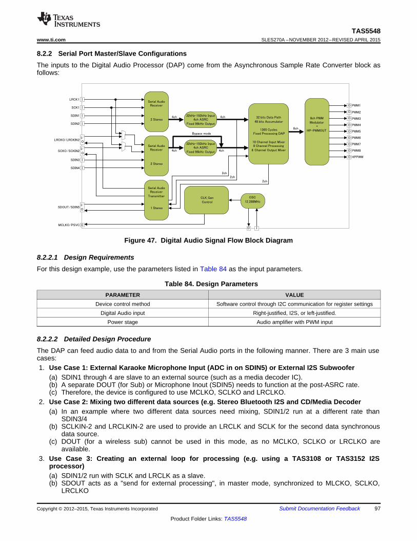
CLK_Gen
Control
LRCK1
SCK1
SDIN1
SDIN2
8ch PWM
Modulator
+
HP-PWMOUT
32kHz–192kHz Input
4ch ASRC
Fixed 96kHz Output
32 bits Data Path
48 bits Accumulator
1365 Cycles
Fixed Processing DAP
10 Channel Input Mixer
8 Channel Processing
8 Channel Output Mixer
32kHz–192kHz Input
4ch ASRC
Fixed 96kHz Output
Serial Audio
Receiver
4ch2 Stereo
Serial Audio
Receiver 4ch
2 Stereo
LRCKO/LRCKIN2
SCKO/SCKIN2
SDIN3
SDIN4
4ch
4ch
Serial Audio
Receiver
Transmitter
1 StereoSDOUT/SDIN5
I/
O
I
O
I
I
I
I
I
I/
O
I/
O
MCLKO/PSVC
OSC
12.288MHz
8ch
O
O
O
O
O
O
O
O
O
IO
2ch
2ch
Bypass mode
2ch
HPPWM
PWM8
PWM7
PWM6
PWM5
PWM4
PWM3
PWM2
PWM1
TAS5548www.ti.com SLES270A –NOVEMBER 2012–REVISED APRIL 2015
8.2.2 Serial Port Master/Slave ConfigurationsThe inputs to the Digital Audio Processor (DAP) come from the Asynchronous Sample Rate Converter block asfollows:
Figure 47. Digital Audio Signal Flow Block Diagram
8.2.2.1 Design RequirementsFor this design example, use the parameters listed in Table 84 as the input parameters.
Table 84. Design ParametersPARAMETER VALUE
Device control method Software control through I2C communication for register settingsDigital Audio input Right-justified, I2S, or left-justified.
Power stage Audio amplifier with PWM input
8.2.2.2 Detailed Design ProcedureThe DAP can feed audio data to and from the Serial Audio ports in the following manner. There are 3 main usecases:1. Use Case 1: External Karaoke Microphone Input (ADC in on SDIN5) or External I2S Subwoofer
(a) SDIN1 through 4 are slave to an external source (such as a media decoder IC).(b) A separate DOUT (for Sub) or Microphone Inout (SDIN5) needs to function at the post-ASRC rate.(c) Therefore, the device is configured to use MCLKO, SCLKO and LRCLKO.
2. Use Case 2: Mixing two different data sources (e.g. Stereo Bluetooth I2S and CD/Media Decoder(a) In an example where two different data sources need mixing, SDIN1/2 run at a different rate than
SDIN3/4(b) SCLKIN-2 and LRCLKIN-2 are used to provide an LRCLK and SCLK for the second data synchronous
data source.(c) DOUT (for a wireless sub) cannot be used in this mode, as no MCLKO, SCLKO or LRCLKO are
available.3. Use Case 3: Creating an external loop for processing (e.g. using a TAS3108 or TAS3152 I2S
processor)(a) SDIN1/2 run with SCLK and LRCLK as a slave.(b) SDOUT acts as a "send for external processing", in master mode, synchronized to MLCKO, SCLKO,
LRCLKO
Copyright © 2012–2015, Texas Instruments Incorporated Submit Documentation Feedback 97
Product Folder Links: TAS5548
HPPWM
PWM8
PWM7
PWM6
PWM5
PWM4
PWM3
PWM2
PWM1
MCLKI
SDIN
SDOUT1
SDOUT2
SCKI
LRCKI
TAS3108
Audio Source
CLK_Gen
Control
LRCK1
SCK1
SDIN1
SDIN2
8ch PWM
Modulator
+
HP-PWMOUT
32kHz–192kHz Input
4ch ASRC
Fixed 96kHz Output
32 bits Data Path
48 bits Accumulator
1365 Cycles
Fixed Processing DAP
10 Channel Input Mixer
8 Channel Processing
8 Channel Output Mixer
32kHz–192kHz Input
4ch ASRC
Fixed 96kHz Output
Serial Audio
Receiver
4ch2 Stereo
Serial Audio
Receiver 4ch
2 Stereo
LRCKO/LRCKIN2
SCKO/SCKIN2
SDIN3
SDIN4
4ch
4ch
Serial Audio
Receiver
Transmitter
1 StereoSDOUT/SDIN5
I/
O
I
O
I
I
I
I
I
I/
O
I/
O
MCLKO/PSVC
OSC
12.288MHz
8ch
O
O
O
O
O
O
O
O
O
IO
SDOUT
MCLKO
2ch
2ch
Bypass mode
2ch
TAS5548SLES270A –NOVEMBER 2012–REVISED APRIL 2015 www.ti.com
(c) SDIN3/4 Act as a "return from external processing", in master mode, synchronized to MLCKO, SCLKO,LRCLKO
Table 85. Master/Slave Serial Audio Receiver/TransmitterSlave Serial Audio port Master Serial Audio port
• To ASRC1 and ASRC2– SCLK LRCLK • MCLKO– Synchronous data • SCLKO
Use case-1 • LRCLKO– SDIN1• Synchronous data– SDIN2
– SDIN5(mic) or SDOUT– SDIN3– SDIN4
• To ASRC1– SCLK– LRCLK– Synchronous data
– SDIN1– SDIN2Use case-2 None of Master
• To ASRC2– SCLKIN-2– LRCLKIN-2– Synchronous data
– SDIN2-1– SDIN2-2
• MLCKO• To ASRC1 • SCLKO– SCLK • LRCLKO– LRCLKUse case-3 • Synchronous data– Synchronous data – SDIN2-1 (ASRC2)
– SDIN1 – SDIN2-2 (ASRC2)– SDIN2 – SDIN5 or SDOUT
By using use case-3, TAS5548 can connect TAS3108 as external co-processor as follows:
Figure 48. TAS3108 as External Co-processor
98 Submit Documentation Feedback Copyright © 2012–2015, Texas Instruments Incorporated
Product Folder Links: TAS5548

Frequency (Hz)
Am
plitu
de (
dB)
0 5000 10000 15000 20000 25000-200
-180
-160
-140
-120
-100
-80
-60
-40
-20
0
D006
TAS5548www.ti.com SLES270A –NOVEMBER 2012–REVISED APRIL 2015
8.2.2.3 Application Curves
Figure 49. Frequency Response at 48 kHz Sampling Rate with -60 dB Input at 1 kHz
Copyright © 2012–2015, Texas Instruments Incorporated Submit Documentation Feedback 99
Product Folder Links: TAS5548
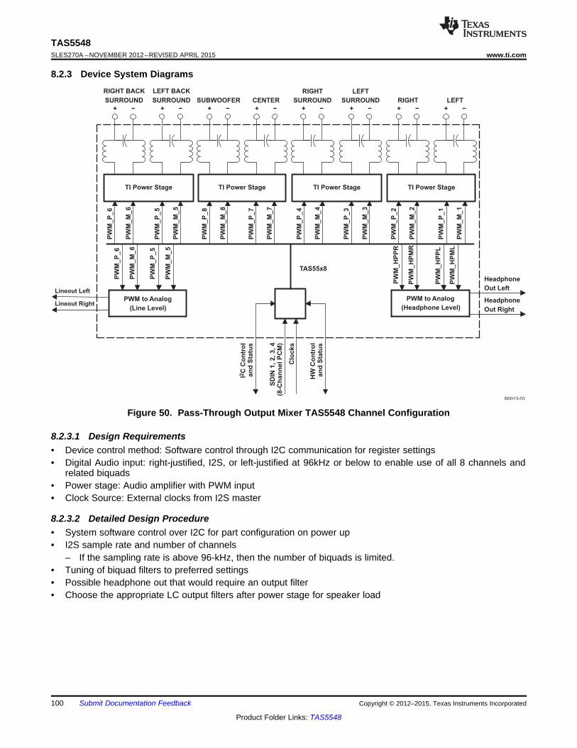
TAS55x8
TI Power Stage
+
PW
M_M
_1
PW
M_P
_1
PW
M_M
_2
PW
M_P
_2
PW
M_M
_3
PW
M_P
_3
PW
M_M
_4
PW
M_P
_4
PW
M_M
_7
PW
M_P
_7
PW
M_M
_8
PW
M_P
_8
PW
M_M
_5
PW
M_P
_5
PW
M_M
_6
PW
M_P
_6
LEFTRIGHT
LEFT
SURROUNDCENTERSUBWOOFER
RIGHT
SURROUND
LEFT BACK
SURROUND
RIGHT BACK
SURROUND
PWM to Analog
(Line Level)
PWM to Analog
(Headphone Level)Headphone
Out Right
Headphone
Out Left
PW
M_H
PM
L
PW
M_H
PP
L
PW
M_H
PM
R
PW
M_H
PP
R
PW
M_M
_5
PW
M_P
_5
PW
M_M
_6
PW
M_P
_6
B0013-03
I2C
Co
ntr
ol
an
d S
tatu
s
SD
IN 1
, 2, 3, 4
(8-C
han
nel P
CM
)
Clo
cks
HW
Co
ntr
ol
an
d S
tatu
s
Lineout Left
Lineout Right
− + − + − + − + − + − + − + −
TI Power Stage TI Power Stage TI Power Stage
TAS5548SLES270A –NOVEMBER 2012–REVISED APRIL 2015 www.ti.com
8.2.3 Device System Diagrams
Figure 50. Pass-Through Output Mixer TAS5548 Channel Configuration
8.2.3.1 Design Requirements• Device control method: Software control through I2C communication for register settings• Digital Audio input: right-justified, I2S, or left-justified at 96kHz or below to enable use of all 8 channels and
related biquads• Power stage: Audio amplifier with PWM input• Clock Source: External clocks from I2S master
8.2.3.2 Detailed Design Procedure• System software control over I2C for part configuration on power up• I2S sample rate and number of channels
– If the sampling rate is above 96-kHz, then the number of biquads is limited.• Tuning of biquad filters to preferred settings• Possible headphone out that would require an output filter• Choose the appropriate LC output filters after power stage for speaker load
100 Submit Documentation Feedback Copyright © 2012–2015, Texas Instruments Incorporated
Product Folder Links: TAS5548
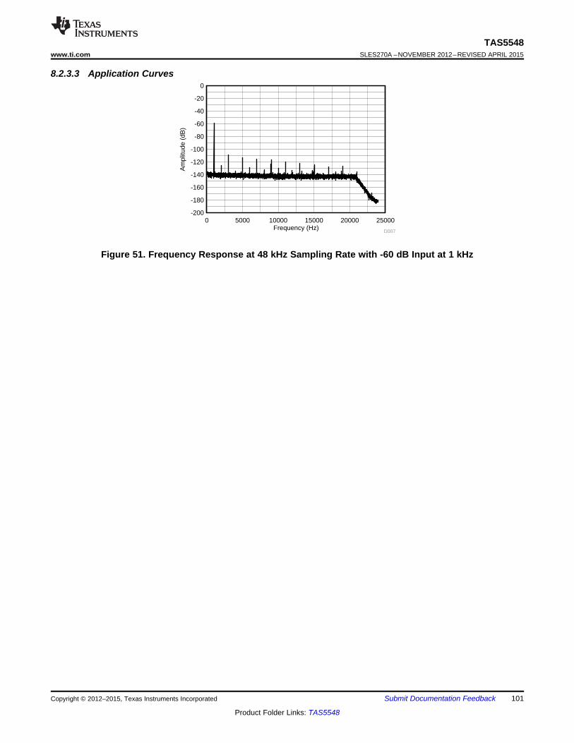
Frequency (Hz)
Am
plitu
de (
dB)
0 5000 10000 15000 20000 25000-200
-180
-160
-140
-120
-100
-80
-60
-40
-20
0
D007
TAS5548www.ti.com SLES270A –NOVEMBER 2012–REVISED APRIL 2015
8.2.3.3 Application Curves
Figure 51. Frequency Response at 48 kHz Sampling Rate with -60 dB Input at 1 kHz
Copyright © 2012–2015, Texas Instruments Incorporated Submit Documentation Feedback 101
Product Folder Links: TAS5548
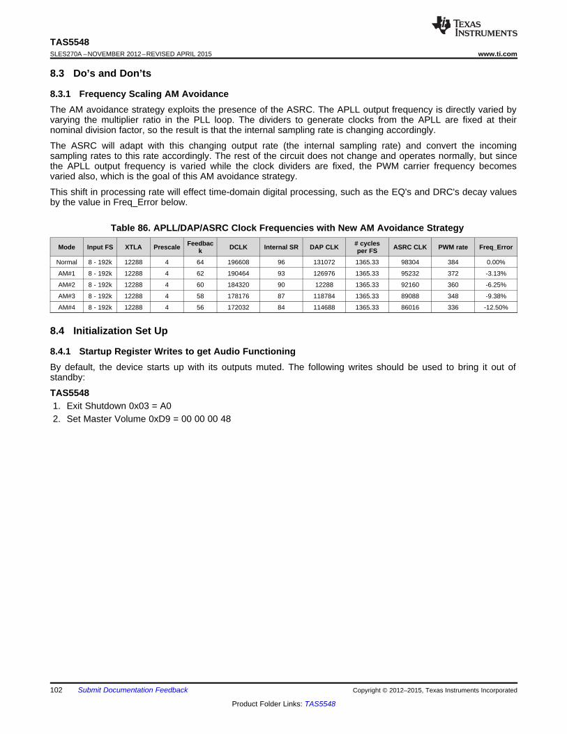
TAS5548SLES270A –NOVEMBER 2012–REVISED APRIL 2015 www.ti.com
8.3 Do’s and Don’ts
8.3.1 Frequency Scaling AM AvoidanceThe AM avoidance strategy exploits the presence of the ASRC. The APLL output frequency is directly varied byvarying the multiplier ratio in the PLL loop. The dividers to generate clocks from the APLL are fixed at theirnominal division factor, so the result is that the internal sampling rate is changing accordingly.
The ASRC will adapt with this changing output rate (the internal sampling rate) and convert the incomingsampling rates to this rate accordingly. The rest of the circuit does not change and operates normally, but sincethe APLL output frequency is varied while the clock dividers are fixed, the PWM carrier frequency becomesvaried also, which is the goal of this AM avoidance strategy.
This shift in processing rate will effect time-domain digital processing, such as the EQ's and DRC's decay valuesby the value in Freq_Error below.
Table 86. APLL/DAP/ASRC Clock Frequencies with New AM Avoidance StrategyFeedbac # cyclesMode Input FS XTLA Prescale DCLK Internal SR DAP CLK ASRC CLK PWM rate Freq_Errork per FS
Normal 8 - 192k 12288 4 64 196608 96 131072 1365.33 98304 384 0.00%
AM#1 8 - 192k 12288 4 62 190464 93 126976 1365.33 95232 372 -3.13%
AM#2 8 - 192k 12288 4 60 184320 90 12288 1365.33 92160 360 -6.25%
AM#3 8 - 192k 12288 4 58 178176 87 118784 1365.33 89088 348 -9.38%
AM#4 8 - 192k 12288 4 56 172032 84 114688 1365.33 86016 336 -12.50%
8.4 Initialization Set Up
8.4.1 Startup Register Writes to get Audio FunctioningBy default, the device starts up with its outputs muted. The following writes should be used to bring it out ofstandby:
TAS55481. Exit Shutdown 0x03 = A02. Set Master Volume 0xD9 = 00 00 00 48
102 Submit Documentation Feedback Copyright © 2012–2015, Texas Instruments Incorporated
Product Folder Links: TAS5548
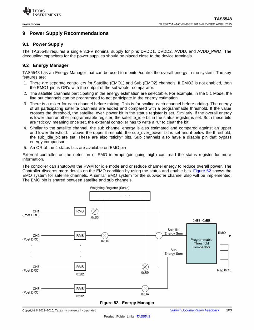
CH1(Post DRC)
RMS
Weighting Register (Scale)
. . .
CH2(Post DRC)
.
.
.
.
.
.
SatalliteEnergy Sum
ProgrammableThreshold
Comparator
EMO
CH7(Post DRC)
0xBB–0xBE
Reg 0x10
0xB2
RMS
RMS
0xB3
0xB4
0xB9
CH8(Post DRC)
0xB2
RMS
0xBA
SubEnergy Sum
TAS5548www.ti.com SLES270A –NOVEMBER 2012–REVISED APRIL 2015
9 Power Supply Recommendations
9.1 Power SupplyThe TAS5548 requires a single 3.3-V nominal supply for pins DVDD1, DVDD2, AVDD, and AVDD_PWM. Thedecoupling capacitors for the power supplies should be placed close to the device terminals.
9.2 Energy ManagerTAS5548 has an Energy Manager that can be used to monitor/control the overall energy in the system. The keyfeatures are:1. There are separate controllers for Satellite (EMO1) and Sub (EMO2) channels. If EMO2 is not enabled, then
the EMO1 pin is OR'd with the output of the subwoofer comparator.2. The satellite channels participating in the energy estimation are selectable. For example, in the 5.1 Mode, the
line out channels can be programmed to not participate in the energy estimation.3. There is a mixer for each channel before mixing. This is for scaling each channel before adding. The energy
of all participating satellite channels are added and compared with a programmable threshold. If the valuecrosses the threshold, the satellite_over_power bit in the status register is set. Similarly, if the overall energyis lower than another programmable register, the satellite_idle bit in the status register is set. Both these bitsare “sticky,” meaning once set, the external controller has to write a “0” to clear the bit
4. Similar to the satellite channel, the sub channel energy is also estimated and compared against an upperand lower threshold. If above the upper threshold, the sub_over_power bit is set and if below the threshold,the sub_idle_bit are set. These are also "sticky" bits. Sub channels also have a disable pin that bypassenergy comparison.
5. An OR of the 4 status bits are available on EMO pin
External controller on the detection of EMO interrupt (pin going high) can read the status register for moreinformation.
The controller can shutdown the PWM for idle mode and or reduce channel energy to reduce overall power. TheController discerns more details on the EMO condition by using the status and enable bits. Figure 52 shows theEMO system for satellite channels. A similar EMO system for the subwoofer channel also will be implemented.The EMO pin is shared between satellite and sub channels.
Figure 52. Energy ManagerCopyright © 2012–2015, Texas Instruments Incorporated Submit Documentation Feedback 103
Product Folder Links: TAS5548
TAS5548SLES270A –NOVEMBER 2012–REVISED APRIL 2015 www.ti.com
9.3 Programming Energy ManagerEnergy Manager related registers are 0xBA to 0xBE. 0xB2 is a 16 byte averaging filter (alpha filter) for bothsatellite and sub channel. The scaling coefficients are 0xB3 to 0xBA that multiplies energy of each channel with ascaling factor. The threshold registers are (0xBB, 0xBC, 0xBD and 0xBE) and 0x10 for the results register.
Table 87. Energy Manager Status Register (x10)D3 D2 D1 D0 FUNCTION– – – 0/1 Energy below the low threshold for satellite channels– – 0/1 – Energy above the high threshold for satellite channels– 0/1 – – Energy below the low threshold for sub-woofer
channel0/1 – – – Energy above the high threshold for sub-woofer
channels
Provision to read the whole byte and a way to clear the 4 LSBs (one by one).
104 Submit Documentation Feedback Copyright © 2012–2015, Texas Instruments Incorporated
Product Folder Links: TAS5548
TAS5548www.ti.com SLES270A –NOVEMBER 2012–REVISED APRIL 2015
10 Layout
10.1 Layout Guidelines• The TAS5548 uses the PCB as a heat sink; therefore, the PowerPAD must be soldered to the PCB, and
adequate copper areas and copper vias connecting the top, bottom, and internal layers should be used.• Decoupling capacitors should be placed as close to the DVDD1_CORE, DVDD2_CORE, VR_DIG,
AVDD_PWM and AVDD as possible. These decoupling capacitors should also have a path through the GNDplane back to the power pad, as shown by the blue area in the layout example in Figure 53.
• A single common GND plane between AGND and DGND is recommended to avoid a potential voltagedifference between them. Multiple vias from the TAS5548 PowerPAD should be connected to GND with alarge copper pad as well as vias to all GND planes.
• Further guidelines can be found on the layout example in Figure 53.• A more detailed example of the PCB layout can be found in the TAS5548EVM User's Guide (SLOU351).
Copyright © 2012–2015, Texas Instruments Incorporated Submit Documentation Feedback 105
Product Folder Links: TAS5548
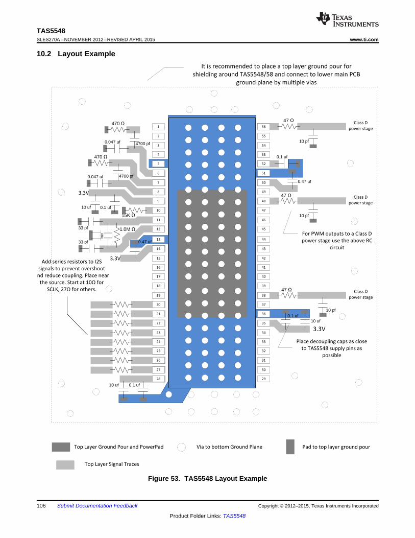
Top Layer Ground Pour and PowerPad
Top Layer Signal Traces
Via to bottom Ground Plane Pad to top layer ground pour
It is recommended to place a top layer ground pour for
shielding around TAS5548/58 and connect to lower main PCB
ground plane by multiple vias
Class D
power stage
Class D
power stage
27
28
25
26
23
24
21
22
19
20
17
18
15
16
13
14
11
12
9
10
7
8
5
6
4
1
2
30
29
32
31
34
33
36
35
38
37
40
39
42
41
44
43
46
45
48
47
50
49
52
51
54
53
56
55
3
3.3V
GN
D
3.3V
Class D
power stage
For PWM outputs to a Class D
power stage use the above RC
circuit
3.3V
Place decoupling caps as close
to TAS5548 supply pins as
possible
470
470
0.047 uf 4700 pf
47
4700 pf0.047 uf
10 uf 0.1 uf
15K
33 pf
33 pf
1.0M
0.47 uf
10 uf 0.1 uf
0.1 uf10 uf
47
10 pf
10 pf
47
0.1 uf
10 pf
0.47 uf
Add series resistors to I2S
signals to prevent overshoot
and reduce coupling. Place near
the source. Start at 10Q(
SCLK, 27Q(Z.
TAS5548SLES270A –NOVEMBER 2012–REVISED APRIL 2015 www.ti.com
10.2 Layout Example
Figure 53. TAS5548 Layout Example
106 Submit Documentation Feedback Copyright © 2012–2015, Texas Instruments Incorporated
Product Folder Links: TAS5548
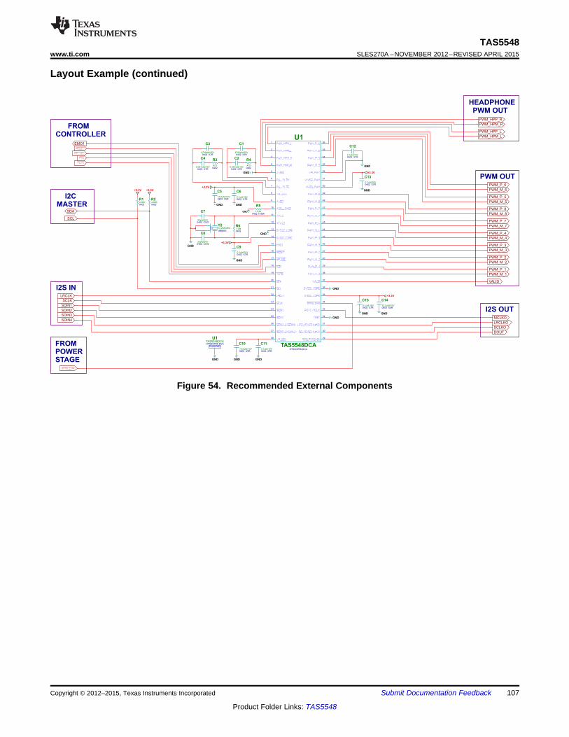
SCL
PWM_P_3
PWM_M_4
PWM_P_4
PWM_P_8
PWM_M_8
PWM_M_7
PWM_P_7
SDA
SDIN4
LRCLK
SCLK
SDIN1
SDIN2
SDIN3MCLKO
LRCLKO
SCLKO
DOUT
PWM_HPP_R
PWM_HPM_R
PWM_HPP_L
PWM_HPM_L
PWM_P_2
PWM_M_3
PWM_M_2
PWM_P_1
PWM_M_1
VALID
PWM_M_5
PWM_P_5
PWM_M_6
PWM_P_6
EMO1
HTSSOP56-DCA
TAS5548DCA
U1
29
56
55
54
53
52
51
50
49
48
47
46
45
44
43
42
41
40
39
38
37
36
35
34
33
32
31
30
28
27
26
25
24
23
22
21
20
19
18
17
16
15
14
13
12
11
10
9
8
7
6
5
4
3
2
1
GND
4700pfd/25V0402 X7R
C3
4700402
R3
0.047ufd/16V0402 X7R
C4
4700pfd/25V0402 X7R
C1
4700402
R4
0.047ufd/16V0402 X7R
C2
15.0K0402 1/16W
R5
GND
GND
0.1ufd/16V0402 X7R
C6
GND
10.0ufd/10V0603 X5R
C5
+3.3V
GND
0.1ufd/16V0402 X7R
C9
GND
+3.3V
33pfd/50V0402 COG
C7
33pfd/50V0402 COG
C8
12.288 MHz
ABM8G
Y2
GN
D
1.0M0402
R6
GND
10.0ufd/10V0603 X5R
C10
0.1ufd/16V0402 X7R
C11
GND GNDGND
0.1ufd/16V0402 X7R
C15
GND
10.0ufd/10V0603 X5R
C14
GND
+3.3V
0.1ufd/16V0402 X7R
C12
GND
0.1ufd/16V0402 X7R
C13
GND
+3.3V
TAS5548DCAHTSSOP56-DCA
U1
PowerPAD
04024.99KR2
+3.3V
4.99K0402
R1
+3.3V
GND
GND
PWM OUT
I2S OUT
FROM
POWER
STAGE
I2S IN
HEADPHONE
PWM OUT
FROM
CONTROLLER
I2C
MASTER
TAS5548www.ti.com SLES270A –NOVEMBER 2012–REVISED APRIL 2015
Layout Example (continued)
Figure 54. Recommended External Components
Copyright © 2012–2015, Texas Instruments Incorporated Submit Documentation Feedback 107
Product Folder Links: TAS5548
TAS5548SLES270A –NOVEMBER 2012–REVISED APRIL 2015 www.ti.com
11 Device and Documentation Support
11.1 Documentation Support
11.1.1 Related DocumentationFor related documentation, see the following:
TAS5548EVM User's Guide (SLOU351)
11.2 TrademarksMatlab is a trademark of Math Works, Inc.All other trademarks are the property of their respective owners.
11.3 Electrostatic Discharge CautionThese devices have limited built-in ESD protection. The leads should be shorted together or the device placed in conductive foamduring storage or handling to prevent electrostatic damage to the MOS gates.
11.4 GlossarySLYZ022 — TI Glossary.
This glossary lists and explains terms, acronyms, and definitions.
12 Mechanical, Packaging, and Orderable InformationThe following pages include mechanical, packaging, and orderable information. This information is the mostcurrent data available for the designated devices. This data is subject to change without notice and revision ofthis document. For browser-based versions of this data sheet, refer to the left-hand navigation.
108 Submit Documentation Feedback Copyright © 2012–2015, Texas Instruments Incorporated
Product Folder Links: TAS5548
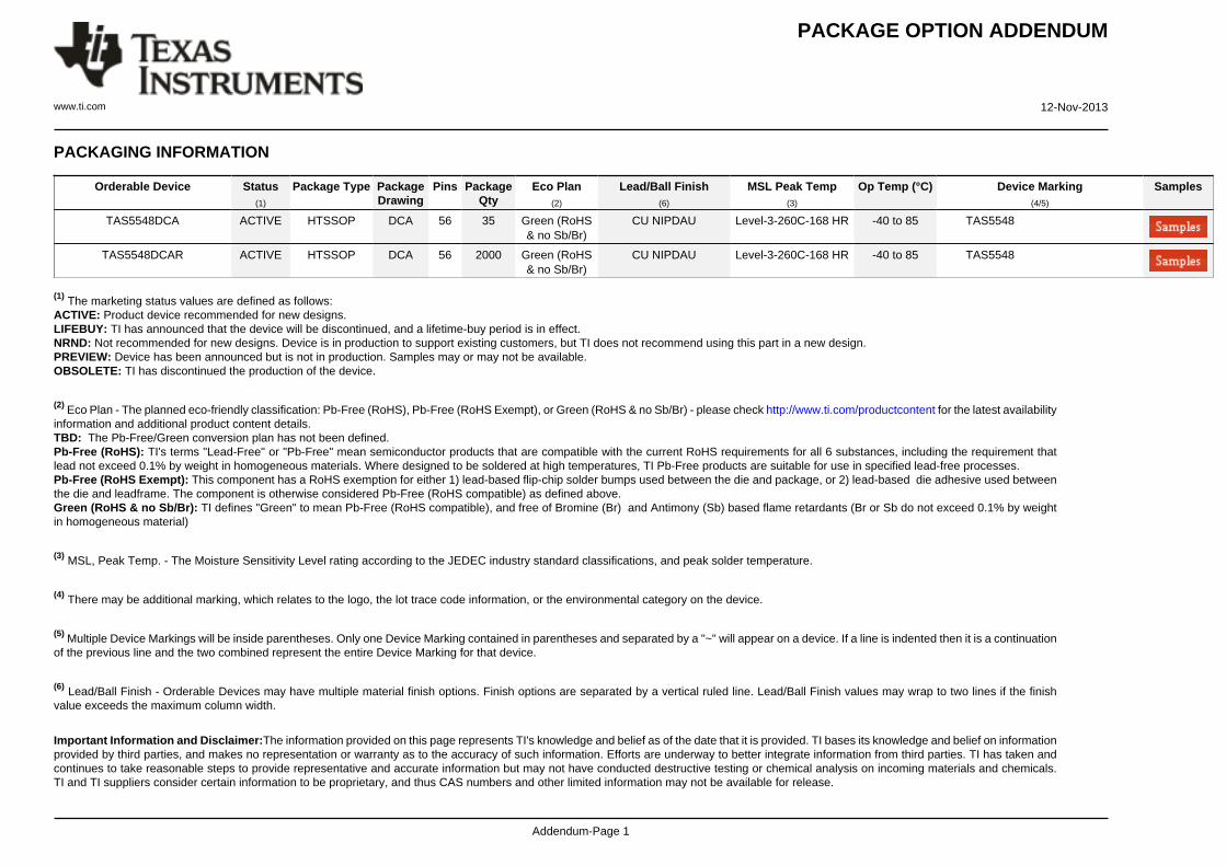
PACKAGE OPTION ADDENDUM
www.ti.com 12-Nov-2013
Addendum-Page 1
PACKAGING INFORMATION
Orderable Device Status(1)
Package Type PackageDrawing
Pins PackageQty
Eco Plan(2)
Lead/Ball Finish(6)
MSL Peak Temp(3)
Op Temp (°C) Device Marking(4/5)
Samples
TAS5548DCA ACTIVE HTSSOP DCA 56 35 Green (RoHS& no Sb/Br)
CU NIPDAU Level-3-260C-168 HR -40 to 85 TAS5548
TAS5548DCAR ACTIVE HTSSOP DCA 56 2000 Green (RoHS& no Sb/Br)
CU NIPDAU Level-3-260C-168 HR -40 to 85 TAS5548
(1) The marketing status values are defined as follows:ACTIVE: Product device recommended for new designs.LIFEBUY: TI has announced that the device will be discontinued, and a lifetime-buy period is in effect.NRND: Not recommended for new designs. Device is in production to support existing customers, but TI does not recommend using this part in a new design.PREVIEW: Device has been announced but is not in production. Samples may or may not be available.OBSOLETE: TI has discontinued the production of the device.
(2) Eco Plan - The planned eco-friendly classification: Pb-Free (RoHS), Pb-Free (RoHS Exempt), or Green (RoHS & no Sb/Br) - please check http://www.ti.com/productcontent for the latest availabilityinformation and additional product content details.TBD: The Pb-Free/Green conversion plan has not been defined.Pb-Free (RoHS): TI's terms "Lead-Free" or "Pb-Free" mean semiconductor products that are compatible with the current RoHS requirements for all 6 substances, including the requirement thatlead not exceed 0.1% by weight in homogeneous materials. Where designed to be soldered at high temperatures, TI Pb-Free products are suitable for use in specified lead-free processes.Pb-Free (RoHS Exempt): This component has a RoHS exemption for either 1) lead-based flip-chip solder bumps used between the die and package, or 2) lead-based die adhesive used betweenthe die and leadframe. The component is otherwise considered Pb-Free (RoHS compatible) as defined above.Green (RoHS & no Sb/Br): TI defines "Green" to mean Pb-Free (RoHS compatible), and free of Bromine (Br) and Antimony (Sb) based flame retardants (Br or Sb do not exceed 0.1% by weightin homogeneous material)
(3) MSL, Peak Temp. - The Moisture Sensitivity Level rating according to the JEDEC industry standard classifications, and peak solder temperature.
(4) There may be additional marking, which relates to the logo, the lot trace code information, or the environmental category on the device.
(5) Multiple Device Markings will be inside parentheses. Only one Device Marking contained in parentheses and separated by a "~" will appear on a device. If a line is indented then it is a continuationof the previous line and the two combined represent the entire Device Marking for that device.
(6) Lead/Ball Finish - Orderable Devices may have multiple material finish options. Finish options are separated by a vertical ruled line. Lead/Ball Finish values may wrap to two lines if the finishvalue exceeds the maximum column width.
Important Information and Disclaimer:The information provided on this page represents TI's knowledge and belief as of the date that it is provided. TI bases its knowledge and belief on informationprovided by third parties, and makes no representation or warranty as to the accuracy of such information. Efforts are underway to better integrate information from third parties. TI has taken andcontinues to take reasonable steps to provide representative and accurate information but may not have conducted destructive testing or chemical analysis on incoming materials and chemicals.TI and TI suppliers consider certain information to be proprietary, and thus CAS numbers and other limited information may not be available for release.
PACKAGE OPTION ADDENDUM
www.ti.com 12-Nov-2013
Addendum-Page 2
In no event shall TI's liability arising out of such information exceed the total purchase price of the TI part(s) at issue in this document sold by TI to Customer on an annual basis.
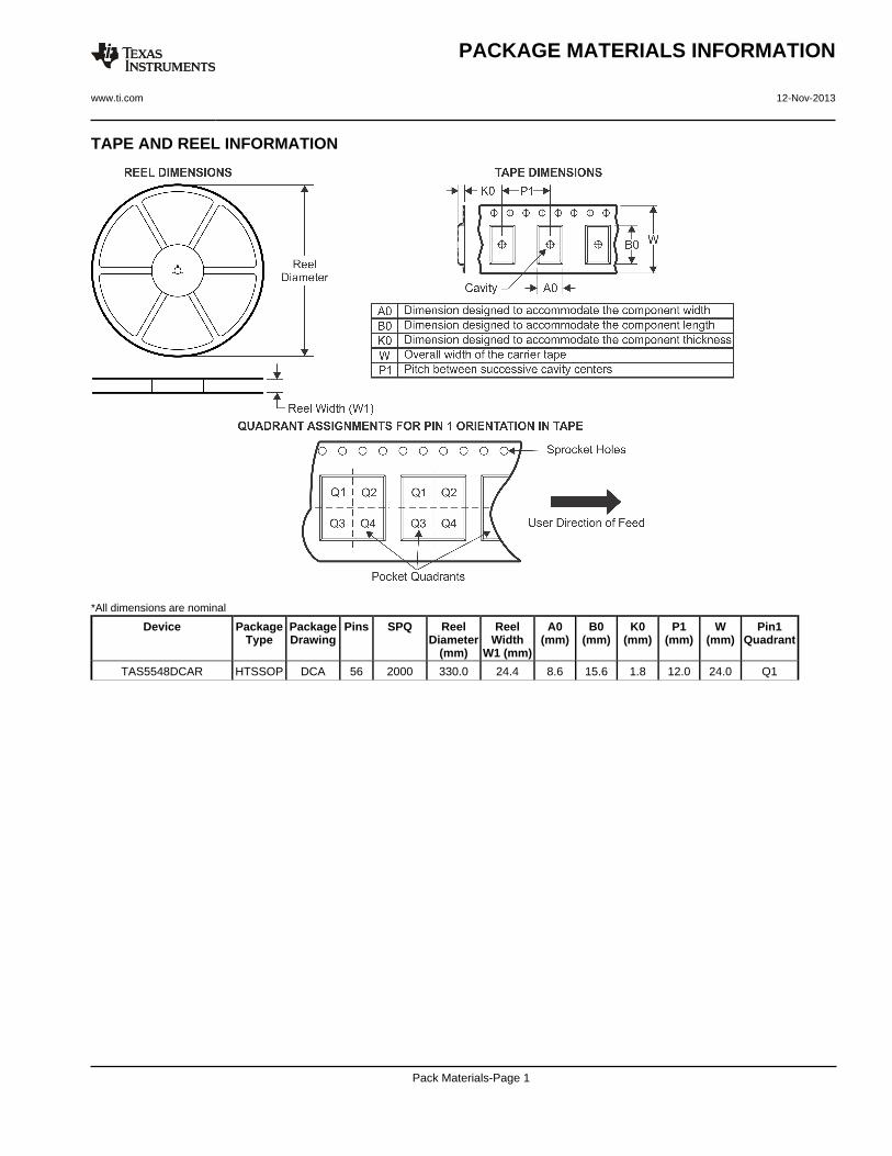
TAPE AND REEL INFORMATION
*All dimensions are nominal
Device PackageType
PackageDrawing
Pins SPQ ReelDiameter
(mm)
ReelWidth
W1 (mm)
A0(mm)
B0(mm)
K0(mm)
P1(mm)
W(mm)
Pin1Quadrant
TAS5548DCAR HTSSOP DCA 56 2000 330.0 24.4 8.6 15.6 1.8 12.0 24.0 Q1
PACKAGE MATERIALS INFORMATION
www.ti.com 12-Nov-2013
Pack Materials-Page 1
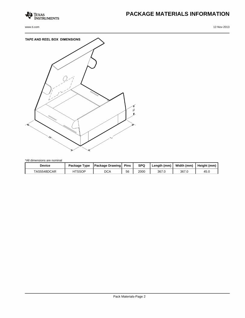
*All dimensions are nominal
Device Package Type Package Drawing Pins SPQ Length (mm) Width (mm) Height (mm)
TAS5548DCAR HTSSOP DCA 56 2000 367.0 367.0 45.0
PACKAGE MATERIALS INFORMATION
www.ti.com 12-Nov-2013
Pack Materials-Page 2
IMPORTANT NOTICE
Texas Instruments Incorporated and its subsidiaries (TI) reserve the right to make corrections, enhancements, improvements and otherchanges to its semiconductor products and services per JESD46, latest issue, and to discontinue any product or service per JESD48, latestissue. Buyers should obtain the latest relevant information before placing orders and should verify that such information is current andcomplete. All semiconductor products (also referred to herein as “components”) are sold subject to TI’s terms and conditions of salesupplied at the time of order acknowledgment.TI warrants performance of its components to the specifications applicable at the time of sale, in accordance with the warranty in TI’s termsand conditions of sale of semiconductor products. Testing and other quality control techniques are used to the extent TI deems necessaryto support this warranty. Except where mandated by applicable law, testing of all parameters of each component is not necessarilyperformed.TI assumes no liability for applications assistance or the design of Buyers’ products. Buyers are responsible for their products andapplications using TI components. To minimize the risks associated with Buyers’ products and applications, Buyers should provideadequate design and operating safeguards.TI does not warrant or represent that any license, either express or implied, is granted under any patent right, copyright, mask work right, orother intellectual property right relating to any combination, machine, or process in which TI components or services are used. Informationpublished by TI regarding third-party products or services does not constitute a license to use such products or services or a warranty orendorsement thereof. Use of such information may require a license from a third party under the patents or other intellectual property of thethird party, or a license from TI under the patents or other intellectual property of TI.Reproduction of significant portions of TI information in TI data books or data sheets is permissible only if reproduction is without alterationand is accompanied by all associated warranties, conditions, limitations, and notices. TI is not responsible or liable for such altereddocumentation. Information of third parties may be subject to additional restrictions.Resale of TI components or services with statements different from or beyond the parameters stated by TI for that component or servicevoids all express and any implied warranties for the associated TI component or service and is an unfair and deceptive business practice.TI is not responsible or liable for any such statements.Buyer acknowledges and agrees that it is solely responsible for compliance with all legal, regulatory and safety-related requirementsconcerning its products, and any use of TI components in its applications, notwithstanding any applications-related information or supportthat may be provided by TI. Buyer represents and agrees that it has all the necessary expertise to create and implement safeguards whichanticipate dangerous consequences of failures, monitor failures and their consequences, lessen the likelihood of failures that might causeharm and take appropriate remedial actions. Buyer will fully indemnify TI and its representatives against any damages arising out of the useof any TI components in safety-critical applications.In some cases, TI components may be promoted specifically to facilitate safety-related applications. With such components, TI’s goal is tohelp enable customers to design and create their own end-product solutions that meet applicable functional safety standards andrequirements. Nonetheless, such components are subject to these terms.No TI components are authorized for use in FDA Class III (or similar life-critical medical equipment) unless authorized officers of the partieshave executed a special agreement specifically governing such use.Only those TI components which TI has specifically designated as military grade or “enhanced plastic” are designed and intended for use inmilitary/aerospace applications or environments. Buyer acknowledges and agrees that any military or aerospace use of TI componentswhich have not been so designated is solely at the Buyer's risk, and that Buyer is solely responsible for compliance with all legal andregulatory requirements in connection with such use.TI has specifically designated certain components as meeting ISO/TS16949 requirements, mainly for automotive use. In any case of use ofnon-designated products, TI will not be responsible for any failure to meet ISO/TS16949.
Products ApplicationsAudio www.ti.com/audio Automotive and Transportation www.ti.com/automotiveAmplifiers amplifier.ti.com Communications and Telecom www.ti.com/communicationsData Converters dataconverter.ti.com Computers and Peripherals www.ti.com/computersDLP® Products www.dlp.com Consumer Electronics www.ti.com/consumer-appsDSP dsp.ti.com Energy and Lighting www.ti.com/energyClocks and Timers www.ti.com/clocks Industrial www.ti.com/industrialInterface interface.ti.com Medical www.ti.com/medicalLogic logic.ti.com Security www.ti.com/securityPower Mgmt power.ti.com Space, Avionics and Defense www.ti.com/space-avionics-defenseMicrocontrollers microcontroller.ti.com Video and Imaging www.ti.com/videoRFID www.ti-rfid.comOMAP Applications Processors www.ti.com/omap TI E2E Community e2e.ti.comWireless Connectivity www.ti.com/wirelessconnectivity
Mailing Address: Texas Instruments, Post Office Box 655303, Dallas, Texas 75265Copyright © 2015, Texas Instruments Incorporated