8-Channel, 24-Bit, Simultaneous Sampling ADC Data Sheet …€¦ · 8-Channel, 24-Bit, Simultaneous...
97
8-Channel, 24-Bit, Simultaneous Sampling ADC Data Sheet AD7770 Rev. D Document Feedback Information furnished by Analog Devices is believed to be accurate and reliable. However, no responsibility is assumed by Analog Devices for its use, nor for any infringements of patents or other rights of third parties that may result from its use. Specifications subject to change without notice. No license is granted by implication or otherwise under any patent or patent rights of Analog Devices. Trademarks and registered trademarks are the property of their respective owners. One Technology Way, P.O. Box 9106, Norwood, MA 02062-9106, U.S.A. Tel: 781.329.4700 ©2016–2018 Analog Devices, Inc. All rights reserved. Technical Support www.analog.com FEATURES 8-channel, 24-bit simultaneous sampling analog-to-digital converter (ADC) Single-ended or true differential inputs Programmable gain amplifier (PGA) per channel (gains of 1, 2, 4, and 8) Low dc input current ±4 nA (differential) and ±8 nA (single-ended) Up to 32 kSPS output data rate (ODR) per channel Programmable ODRs and bandwidth Sample rate converter (SRC) for coherent sampling Sampling rate resolution up to 15.2 × 10 −6 SPS Low latency sinc3 filter path Adjustable phase synchronization Internal 2.5 V reference Two power modes optimizing power dissipation and performance: high resolution mode and low power mode Low resolution successive approximation register (SAR) ADC for system and chip diagnostics Power supply Bipolar (±1.65 V) or unipolar (3.3 V) supplies Digital input/output (I/O) supply: 1.8 V to 3.6 V Performance temperature range: −40°C to +105°C Functional temperature range: −40°C to +125°C Performance Combined ac and dc performance 103 dB dynamic range at 32 kSPS in high resolution mode −109 dB total harmonic distortion (THD) ±9 ppm of FSR integral nonlinearity (INL) ±15 µV offset error ±0.1% FS gain error ±10 ppm/°C typical temperature coefficient APPLICATIONS Protection relays General-purpose data acquisition Industrial process control GENERAL DESCRIPTION The AD7770 is an 8-channel, simultaneous sampling ADC. Eight full sigma-delta (Σ-Δ) ADCs are on chip. The AD7770 provides a low input current to allow direct sensor connection. Each input channel has a programmable gain stage allowing gains of 1, 2, 4, and 8 to map lower amplitude sensor outputs into the full-scale ADC input range, maximizing the dynamic range of the signal chain. The AD7770 accepts a VREF voltage from 1 V up to 3.6 V. The analog inputs accept unipolar (0 V to VREF) or true bipolar (±VREF/2) analog input signals with 3.3 V or ±1.65 V analog supply voltages, respectively for PGAGAIN = 1. The analog inputs can be configured to accept true differential, pseudo differential, or single-ended signals to match different sensor output configurations. Each channel contains a PGA, an ADC modulator and a sinc3, low latency digital filter. An SRC is provided to allow fine resolution control over the AD7770 ODR. This control can be used in applications where the ODR resolution is required to maintain coherency with 0.01 Hz changes in the line frequency. The SRC is programmable through the serial port interface (SPI). The AD7770 implements two different interfaces: a data output interface and SPI control interface. The ADC data output interface is dedicated to transmitting the ADC conversion results from the AD7770 to the processor. The SPI writes to and reads from the AD7770 configuration registers and for the control and reading of data from the SAR ADC. The SPI can also be configured to output the Σ-Δ conversion data. The AD7770 includes a 12-bit SAR ADC. This ADC can be used for AD7770 diagnostics without having to decommission one of the Σ-Δ ADC channels dedicated to system measurement functions. With the use of an external multiplexer, which can be controlled through the three general-purpose input/output pins (GPIOs), and signal conditioning, the SAR ADC can validate the Σ-Δ ADC measurements in applications where functional safety is required. In addition, the AD7770 SAR ADC includes an internal multiplexer to sense internal nodes. The AD7770 contains a 2.5 V reference and reference buffer. The reference has a typical temperature coefficient of 10 ppm/°C. The AD7770 offers two modes of operation: high resolution mode and low power mode. High resolution mode provides a higher dynamic range while consuming 10.75 mW per channel; low power mode consumes just 3.37 mW per channel at a reduced dynamic range specification. The specified operating temperature range is −40°C to +105°C, although the device is operational up to +125°C. Note that throughout this data sheet, certain terms are used to refer to either the multifunction pins or a range of pins. The multi- function pins, such as DCLK0/SDO, are referred to either by the entire pin name or by a single function of the pin, for example, DCLK0, when only that function is relevant. In the case of ranges of pins, AVSSx refers to the following pins: AVSS1A, AVSS1B, AVSS2A, AVSS2B, AVSS3, and AVSS4.
Transcript of 8-Channel, 24-Bit, Simultaneous Sampling ADC Data Sheet …€¦ · 8-Channel, 24-Bit, Simultaneous...

8-Channel, 24-Bit, Simultaneous Sampling ADC
Data Sheet AD7770
Rev. D Document Feedback Information furnished by Analog Devices is believed to be accurate and reliable. However, no responsibility is assumed by Analog Devices for its use, nor for any infringements of patents or other rights of third parties that may result from its use. Specifications subject to change without notice. No license is granted by implication or otherwise under any patent or patent rights of Analog Devices. Trademarks and registered trademarks are the property of their respective owners.
One Technology Way, P.O. Box 9106, Norwood, MA 02062-9106, U.S.A. Tel: 781.329.4700 ©2016–2018 Analog Devices, Inc. All rights reserved. Technical Support www.analog.com
FEATURES 8-channel, 24-bit simultaneous sampling analog-to-digital
converter (ADC) Single-ended or true differential inputs Programmable gain amplifier (PGA) per channel (gains of
1, 2, 4, and 8) Low dc input current
±4 nA (differential) and ±8 nA (single-ended) Up to 32 kSPS output data rate (ODR) per channel Programmable ODRs and bandwidth Sample rate converter (SRC) for coherent sampling
Sampling rate resolution up to 15.2 × 10⁻⁶ SPS Low latency sinc3 filter path Adjustable phase synchronization Internal 2.5 V reference Two power modes optimizing power dissipation and
performance: high resolution mode and low power mode Low resolution successive approximation register (SAR) ADC
for system and chip diagnostics Power supply
Bipolar (±1.65 V) or unipolar (3.3 V) supplies Digital input/output (I/O) supply: 1.8 V to 3.6 V Performance temperature range: −40°C to +105°C Functional temperature range: −40°C to +125°C
Performance Combined ac and dc performance 103 dB dynamic range at 32 kSPS in high resolution mode −109 dB total harmonic distortion (THD) ±9 ppm of FSR integral nonlinearity (INL) ±15 µV offset error ±0.1% FS gain error ±10 ppm/°C typical temperature coefficient
APPLICATIONS Protection relays General-purpose data acquisition Industrial process control
GENERAL DESCRIPTION The AD7770 is an 8-channel, simultaneous sampling ADC. Eight full sigma-delta (Σ-Δ) ADCs are on chip. The AD7770 provides a low input current to allow direct sensor connection. Each input channel has a programmable gain stage allowing gains of 1, 2, 4, and 8 to map lower amplitude sensor outputs into the full-scale ADC input range, maximizing the dynamic range of the signal chain. The AD7770 accepts a VREF voltage from 1 V up to 3.6 V.
The analog inputs accept unipolar (0 V to VREF) or true bipolar (±VREF/2) analog input signals with 3.3 V or ±1.65 V analog supply voltages, respectively for PGAGAIN = 1. The analog inputs can be configured to accept true differential, pseudo differential, or single-ended signals to match different sensor output configurations.
Each channel contains a PGA, an ADC modulator and a sinc3, low latency digital filter. An SRC is provided to allow fine resolution control over the AD7770 ODR. This control can be used in applications where the ODR resolution is required to maintain coherency with 0.01 Hz changes in the line frequency. The SRC is programmable through the serial port interface (SPI). The AD7770 implements two different interfaces: a data output interface and SPI control interface. The ADC data output interface is dedicated to transmitting the ADC conversion results from the AD7770 to the processor. The SPI writes to and reads from the AD7770 configuration registers and for the control and reading of data from the SAR ADC. The SPI can also be configured to output the Σ-Δ conversion data.
The AD7770 includes a 12-bit SAR ADC. This ADC can be used for AD7770 diagnostics without having to decommission one of the Σ-Δ ADC channels dedicated to system measurement functions. With the use of an external multiplexer, which can be controlled through the three general-purpose input/output pins (GPIOs), and signal conditioning, the SAR ADC can validate the Σ-Δ ADC measurements in applications where functional safety is required. In addition, the AD7770 SAR ADC includes an internal multiplexer to sense internal nodes.
The AD7770 contains a 2.5 V reference and reference buffer. The reference has a typical temperature coefficient of 10 ppm/°C.
The AD7770 offers two modes of operation: high resolution mode and low power mode. High resolution mode provides a higher dynamic range while consuming 10.75 mW per channel; low power mode consumes just 3.37 mW per channel at a reduced dynamic range specification.
The specified operating temperature range is −40°C to +105°C, although the device is operational up to +125°C.
Note that throughout this data sheet, certain terms are used to refer to either the multifunction pins or a range of pins. The multi-function pins, such as DCLK0/SDO, are referred to either by the entire pin name or by a single function of the pin, for example, DCLK0, when only that function is relevant. In the case of ranges of pins, AVSSx refers to the following pins: AVSS1A, AVSS1B, AVSS2A, AVSS2B, AVSS3, and AVSS4.

AD7770 Data Sheet
Rev. D | Page 2 of 97
TABLE OF CONTENTS Features .............................................................................................. 1 Applications ....................................................................................... 1 General Description ......................................................................... 1 Revision History ............................................................................... 4 Functional Block Diagram .............................................................. 5 Specifications ..................................................................................... 6
DOUTx Timing Characterististics ........................................... 10 SPI Timing Characterististics ................................................... 11 Synchronization Pins and Reset Timing Characteristics ...... 12 SAR ADC Timing Characterististics ....................................... 13 GPIO SRC Update Timing Characterististics......................... 13
Absolute Maximum Ratings .......................................................... 14 Thermal Resistance .................................................................... 14 ESD Caution ................................................................................ 14
Pin Configuration and Function Descriptions ........................... 15 Typical Performance Characteristics ........................................... 18 Terminology .................................................................................... 31 Theory of Operation ...................................................................... 33
Analog Inputs .............................................................................. 33 Transfer Function ....................................................................... 34 Core Signal Chain....................................................................... 35 Capacitive PGA ........................................................................... 35 Internal Reference and Reference Buffers ............................... 35 Integrated LDOs ......................................................................... 36 Clocking and Sampling .............................................................. 36 Digital Reset and Synchronization Pins .................................. 36 Digital Filtering ........................................................................... 37 Shutdown Mode .......................................................................... 37 Controlling the AD7770 ............................................................ 38 Pin Control Mode ....................................................................... 38 SPI Control .................................................................................. 40 Digital SPI .................................................................................... 43
RMS Noise and Resolution............................................................ 46 High Resolution Mode ............................................................... 46 Low Power Mode ........................................................................ 46
Diagnostics and Monitoring ......................................................... 47 Self Diagnostics Error ................................................................ 47 Monitoring Using the AD7770 SAR ADC (SPI Control Mode) ........................................................................................... 48 Σ-Δ ADC Diagnostics (SPI Control Mode) ............................ 50
Σ-∆ Output Data............................................................................. 51 ADC Conversion Output—Header and Data ........................ 51 SRC (SPI Control Mode) ........................................................... 52 Data Output Interface ................................................................ 53 Calculating the CRC Checksum .............................................. 58
Register Summary .......................................................................... 60 Register Details ............................................................................... 64
Channel 0 Configuration Register ........................................... 64 Channel 1 Configuration Register ........................................... 64 Channel 2 Configuration Register ........................................... 65 Channel 3 Configuration Register ........................................... 65 Channel 4 Configuration Register ........................................... 66 Channel 5 Configuration Register ........................................... 66 Channel 6 Configuration Register ........................................... 67 Channel 7 Configuration Register ........................................... 67 Disable Clocks to ADC Channel Register .............................. 68 Channel 0 Sync Offset Register ................................................ 68 Channel 1 Sync Offset Register ................................................ 68 Channel 2 Sync Offset Register ................................................ 68 Channel 3 Sync Offset Register ................................................ 69 Channel 4 Sync Offset Register ................................................ 69 Channel 5 Sync Offset Register ................................................ 69 Channel 6 Sync Offset Register ................................................ 69 Channel 7 Sync Offset Register ................................................ 69 General User Configuration 1 Register ................................... 70 General User Configuration 2 Register ................................... 70 General User Configuration 3 Register ................................... 71 Data Output Format Register ................................................... 72 Main ADC Meter and Reference Mux Control Register ...... 73 Global Diagnostics Mux Register ............................................. 74 GPIO Configuration Register ................................................... 74 GPIO Data Register.................................................................... 75 Buffer Configuration 1 Register ............................................... 75 Buffer Configuration 2 Register ............................................... 75 Channel 0 Offset Upper Byte Register..................................... 76 Channel 0 Offset Middle Byte Register ................................... 76 Channel 0 Offset Lower Byte Register ..................................... 76 Channel 0 Gain Upper Byte Register ....................................... 76 Channel 0 Gain Middle Byte Register ..................................... 76 Channel 0 Gain Lower Byte Register ....................................... 77

Data Sheet AD7770
Rev. D | Page 3 of 97
Channel 1 Offset Upper Byte Register ..................................... 77 Channel 1 Offset Middle Byte Register .................................... 77 Channel 1 Offset Lower Byte Register ..................................... 77 Channel 1 Gain Upper Byte Register........................................ 78 Channel 1 Gain Middle Byte Register ...................................... 78 Channel 1 Gain Lower Byte Register ........................................ 78 Channel 2 Offset Upper Byte Register ..................................... 78 Channel 2 Offset Middle Byte Register .................................... 78 Channel 2 Offset Lower Byte Register ..................................... 79 Channel 2 Gain Upper Byte Register........................................ 79 Channel 2 Gain Middle Byte Register ...................................... 79 Channel 2 Gain Lower Byte Register ........................................ 79 Channel 3 Offset Upper Byte Register ..................................... 79 Channel 3 Offset Middle Byte Register .................................... 80 Channel 3 Offset Lower Byte Register ..................................... 80 Channel 3 Gain Upper Byte Register........................................ 80 Channel 3 Gain Middle Byte Register ...................................... 80 Channel 3 Gain Lower Byte Register ........................................ 80 Channel 4 Offset Upper Byte Register ..................................... 81 Channel 4 Offset Middle Byte Register .................................... 81 Channel 4 Offset Lower Byte Register ..................................... 81 Channel 4 Gain Upper Byte Register........................................ 81 Channel 4 Gain Middle Byte Register ...................................... 81 Channel 4 Gain Lower Byte Register ........................................ 82 Channel 5 Offset Upper Byte Register ..................................... 82 Channel 5 Offset Middle Byte Register .................................... 82 Channel 5 Offset Lower Byte Register ..................................... 82 Channel 5 Gain Upper Byte Register........................................ 82 Channel 5 Gain Middle Byte Register ...................................... 83 Channel 5 Gain Lower Byte Register ........................................ 83 Channel 6 Offset Upper Byte Register ..................................... 83 Channel 6 Offset Middle Byte Register .................................... 83 Channel 6 Offset Lower Byte Register ..................................... 83 Channel 6 Gain Upper Byte Register........................................ 84 Channel 6 Gain Middle Byte Register ...................................... 84
Channel 6 Gain Lower Byte Register ....................................... 84 Channel 7 Offset Upper Byte Register ..................................... 84 Channel 7 Offset Middle Byte Register .................................... 84 Channel 7 Offset Lower Byte Register ..................................... 85 Channel 7 Gain Upper Byte Register ....................................... 85 Channel 7 Gain Middle Byte Register ...................................... 85 Channel 7 Gain Lower Byte Register ....................................... 85 Channel 0 Status Register .......................................................... 86 Channel 1 Status Register .......................................................... 86 Channel 2 Status Register .......................................................... 87 Channel 3 Status Register .......................................................... 87 Channel 4 Status Register .......................................................... 88 Channel 5 Status Register .......................................................... 88 Channel 6 Status Register .......................................................... 89 Channel 7 Status Register .......................................................... 89 Channel 0/Channel 1 DSP Errors Register.............................. 90 Channel 2/Channel 3 DSP Errors Register.............................. 90 Channel 4/Channel 5 DSP Errors Register.............................. 91 Channel 6/Channel 7 DSP Errors Register.............................. 91 Channel 0 to Channel 7 Error Register Enable Register ....... 92 General Errors Register 1 ........................................................... 92 General Errors Register 1 Enable .............................................. 93 General Errors Register 2 ........................................................... 93 General Errors Register 2 Enable .............................................. 94 Error Status Register 1 ................................................................ 94 Error Status Register 2 ................................................................ 95 Error Status Register 3 ................................................................ 95 Decimation Rate (N) MSB Register ......................................... 95 Decimation Rate (N) LSB Register ........................................... 96 Decimation Rate (IF) MSB Register ......................................... 96 Decimation Rate (IF) LSB Register .......................................... 96 SRC Load Source and Load Update Register .......................... 96
Outline Dimensions ........................................................................ 97 Ordering Guide ........................................................................... 97

AD7770 Data Sheet
Rev. D | Page 4 of 97
REVISION HISTORY 5/2018—Rev. C to Rev. D Change to t22B Parameter, Table 3 ................................................. 11 Changes to AUXAIN± Parameter, Table 7 .................................. 14 Changes to Table 13 ........................................................................ 38 Changes to Σ-Δ Data, ADC Mode Section ................................. 45 Added Figure 105; Renumbered Sequentially ............................ 45 Changes to SRC Group Delay and Latency Section ................... 53 Changed SPI Section to SPI Interface Section ............................ 57 Updated Outline Dimensions ....................................................... 97 Changes to Ordering Guide .......................................................... 97 8/2017—Rev. B to Rev. C Changes to Features Section and General Description Section ....... 1 Change to START Pin Description, Table 9 ................................ 15 Changes to Figure 48 ...................................................................... 24 Change to Digital Reset and Synchronization Pins Section and Internal Reference and Reference Buffers Section ..................... 36 Change to Figure 95 ....................................................................... 37 Changes to Phase Adjustment Section and Table 16 ................. 41 Added Table 17; Renumbered Sequentially ................................ 41 Change to Digital SPI Section ....................................................... 43 Change to Table 25 ......................................................................... 46 10/2016—Rev. A to Rev. B Changes to Figure 45 ...................................................................... 24 Changes to Figure 56, Figure 59, and Figure 61 ......................... 26 Changes to Figure 72 and Figure 73 ............................................. 28 Changes to Figure 76 ...................................................................... 29 Added Figure 82; Renumbered Sequentially .............................. 30 Changes to Figure 86 to Figure 89 ................................................ 34 Changes to SPI Transmission Errors (SPI Control Mode) Section .............................................................................................. 48 Changes to Table 33 and Table 34 ................................................ 51 Changes to SRC Group Delay and Latency Section and Settling Time Section.................................................................................... 53 Changes to Table 39 and Table 40 ................................................ 57 Changes to Calculating the CRC Checksum Section and Table 42 ............................................................................................ 58 Changes to Ordering Guide .......................................................... 97
5/2016—Rev. 0 to Rev. A Change to Features ............................................................................ 1 Changes to Table 1 ............................................................................. 6 Changes to Figure 33 and Figure 36............................................. 21 Change to Figure 78 ....................................................................... 28 4/2016—Revision 0: Initial Version
Data Sheet AD7770
Rev. D | Page 5 of 97
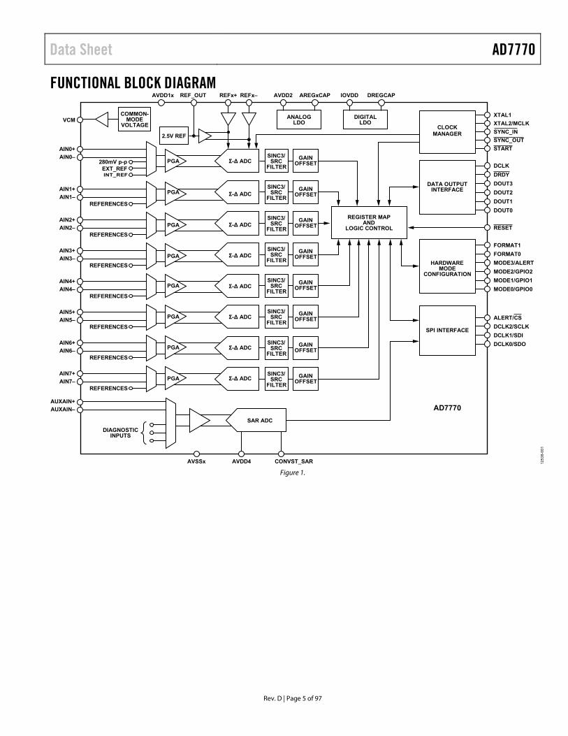
FUNCTIONAL BLOCK DIAGRAM AVDD1x REF_OUT REFx+
VCM
AVDD2
AVSSx AVDD4 CONVST_SAR
IOVDDAREGxCAP DREGCAP
CLOCKMANAGER
XTAL1XTAL2/MCLKSYNC_INSYNC_OUTSTART
REFx–
DCLKDRDYDOUT3DOUT2DOUT1DOUT0
FORMAT1FORMAT0MODE3/ALERTMODE2/GPIO2MODE1/GPIO1MODE0/GPIO0
ALERT/CSDCLK2/SCLKDCLK1/SDIDCLK0/SDO
RESET
Σ-Δ ADC
AIN0+AIN0–
280mV p-p
Σ-Δ ADC
REFERENCES
EXT_REFINT_REF
AIN1+AIN1–
Σ-Δ ADC
REFERENCES
AIN2+AIN2–
Σ-Δ ADC
REFERENCES
AIN3+AIN3–
Σ-Δ ADC
REFERENCES
AIN4+AIN4–
Σ-Δ ADC
REFERENCES
AIN5+AIN5–
REFERENCES
AIN6+AIN6–
REFERENCES
DIAGNOSTICINPUTS
AIN7+AIN7–
SINC3/SRC
FILTERGAIN
OFFSET
COMMON-MODE
VOLTAGEANALOG
LDO
2.5V REF
SINC3/SRC
FILTERGAIN
OFFSET
SINC3/SRC
FILTERGAIN
OFFSET
SINC3/SRC
FILTERGAIN
OFFSET
SINC3/SRC
FILTERGAIN
OFFSET
SINC3/SRC
FILTERGAIN
OFFSET
SINC3/SRC
FILTERGAIN
OFFSET
SINC3/SRC
FILTERGAIN
OFFSET
Σ-Δ ADC
Σ-Δ ADC
AUXAIN+AUXAIN–
DATA OUTPUTINTERFACE
REGISTER MAPAND
LOGIC CONTROL
HARDWAREMODE
CONFIGURATION
SPI INTERFACE
AD7770SAR ADC
DIGITALLDO
PGA
PGA
PGA
PGA
PGA
PGA
PGA
PGA
1253
8-00
1
Figure 1.

AD7770 Data Sheet
Rev. D | Page 6 of 97
SPECIFICATIONS AVDD1x = 1.65 V, AVSSx1 = −1.65 V (dual supply operation), AVDD1x = 3.3 V, AVSSx = analog ground (AGND) (single-supply operation), AVDD2x − AVSSx = 2.2 V to 3.6 V; IOVDD = 1.8 V to 3.6 V; DGND = 0 V, REFx+/REFx− = 2.5 V (internal/external), master clock (MCLK) = 8192 kHz for high resolution mode and 4096 kHz for low power mode, ODR = 32 kSPS for high resolution mode and 8 kSPS for low power mode; all specifications at TMIN to TMAX, unless otherwise noted.
Table 1. Parameter Test Conditions/Comments Min Typ Max Unit ANALOG INPUTS
Differential Input Voltage Range VREF = (REFx+ − REFx−) ±VREF/PGAGAIN V Single-Ended Input Voltage Range 0 to VREF/PGAGAIN V AINx± Common-Mode Input
Range AVSSx + 0.10 (AVDD1x +
AVSSx)/2 AVDD1x − 0.10 V
Absolute AINx± Voltage Limits AVSSx + 0.10 AVDD1x − 0.10 V DC Input Current
Differential High resolution, MCLK = 8192 kHz 4 nA Low power mode, MCLK = 4096 kHz 1 nA
Single-Ended High resolution, MCLK = 8192 kHz 8 nA Low power mode, MCLK = 4096 kHz 2 nA
Input Current Drift 50 pA/°C AC Input Capacitance 8 pF
PGA Gain Settings, PGAGAIN 1, 2, 4, or 8 Bandwidth Small signal, high resolution mode 2 MHz Small signal, low power mode 512 kHz Large signal, high resolution mode 5 kHz Large signal, low power mode 1.5 kHz
REFERENCE Internal
Initial Accuracy REF_OUT, TA = 25°C 2.495 2.5 2.505 V Temperature Coefficient ±10 ±38 ppm/°C Reference Load Current, IL −10 +10 mA DC Power Supply Rejection Line regulation 95 dB Load Regulation, ∆VOUT/∆IL 100 µV/mA Voltage Noise, eN p-p 0.1 Hz to 10 Hz 6.8 µV rms Voltage Noise Density, eN 1 kHz, 2.5 V reference 273.5 nV/√Hz Turn On Settling Time 100 nF 1.5 ms
External Input Voltage VREF = (REFx+ − REFx−) 1 2.5 AVDD1x V Buffer Headroom AVSSx + 0.1 AVDD1x − 0.1 V REFx− Input Voltage AVSSx AVDD1x − REFx+ V Average REFx± Input Current Current per channel
Reference buffer disabled, high resolution mode
18 µA/V
Reference buffer precharge mode (pre-Q), high resolution mode
600 nA/V
Reference buffer disabled, low power mode
4.5 µA/V
Reference buffer pre-Q, low power mode
100 nA/V
Reference buffer enabled, high resolution mode
12 nA/V
Reference buffer enabled, low power mode
5 nA/V

Data Sheet AD7770
Rev. D | Page 7 of 97
Parameter Test Conditions/Comments Min Typ Max Unit TEMPERATURE RANGE
Specified Performance TMIN to TMAX −40 +105 °C Functional2 TMIN to TMAX −40 +125 °C
TEMPERATURE SENSOR Accuracy ±2 °C
DIGITAL FILTER RESPONSE (SINC3) Group Delay See the SRC Group Delay section Settling Time See the Settling Time section Pass Band −0.1 dB See the SRC Bandwidth section −3 dB See the SRC Bandwidth section Decimation Rate 64 4095.99
CLOCK SOURCE Frequency High resolution mode 0.655 8.192 MHz Low power mode 1.3 4.096 MHz Duty Cycle 45:55 50:50 55:45 %
Σ-Δ ADC Speed and Performance
Resolution 24 Bits ODR High resolution mode 32 kSPS Low power mode 8 kSPS No Missing Codes Up to 24 kSPS 24 Bits
AC Accuracy Dynamic Range Shorted inputs, PGAGAIN = 1
32 kSPS High resolution mode 103 dB 8 kSPS High resolution mode 113 dB Low power mode 103 dB 2 kSPS Low power mode 113 dB
THD −0.5 dBFS, high resolution mode −109 dB −0.5 dBFS, low power mode −105 dB Signal-to-Noise-and-Distortion
Ratio (SINAD) fIN = 60 Hz 106 dB
SFDR High resolution mode, 16 kSPS, PGAGAIN = 1
132 dB
Intermodulation Distortion (IMD)
fA = 50 Hz, fB = 51 Hz, high resolution mode
−125 dB
fA = 50 Hz, fB = 51 Hz, low power mode
−105 dB
DC Power Supply Rejection AVDD1x = 3.3 V −90 dB DC Common-Mode Rejection
Ratio 80 dB
Crosstalk −120 dB DC ACCURACY
INL High Resolution Mode Endpoint method, PGAGAIN = 1 ±8 ±15 ppm of FSR Other PGA gains ±4 ±15 ppm of FSR Low Power Mode Endpoint method, PGAGAIN = 1 ±9 ±17 ppm of FSR Other PGA gains ±6 ±15 ppm of FSR
Offset Error ±15 ±90 µV Offset Error Drift ±0.25 µV/°C Over time −2 µV/
1000 hours

AD7770 Data Sheet
Rev. D | Page 8 of 97
Parameter Test Conditions/Comments Min Typ Max Unit Offset Matching 25 µV Gain Error ±0.1 % FS Gain Drift vs. Temperature ±0.75 ppm/°C Gain Matching ±0.1 %
SAR ADC Speed and Performance
Resolution 12 Bits Analog Input Range AVSS4 + 0.1 AVDD4 − 0.1 V Analog Input Common-Mode
Range AVSS4 + 0.1 (AVDD4 +
AVSS4)/2 AVDD4 − 0.1 V
Analog Input Dynamic Current 256 kSPS, 0 dBFS ±100 nA Throughput 256 kSPS
DC Accuracy Differential mode INL 1.5 LSB DNL No missing codes (12-bit) −0.99 +1 LSB Offset ±1 LSB Gain 12 LSB
AC Performance SNR 1 kHz 66 dB THD 1 kHz −81 dB
VCM PIN Output (AVDD1x +
AVSSx)/2 V
Load Current, IL 1 mA Load Regulation, ∆VOUT/∆IL 12 mV/mA Short-Circuit Current 5 mA
LOGIC INPUTS Input Voltage
High, VIH 0.7 × IOVDD V Low, VIL 0.4 V
Hysteresis 0.1 V Input Currents −10 +10 µA
LOGIC OUTPUTS3 Output Voltage
High, VOH IOVDD ≥ 3 V, ISOURCE = 1 mA 0.8 × IOVDD V 2.3 V ≤ IOVDD < 3 V, ISOURCE =
500 μA 0.8 × IOVDD V
IOVDD < 2.3 V, ISOURCE = 200 μA 0.8 × IOVDD V Low, VOL IOVDD ≥ 3 V, ISINK = 2 mA 0.4 V 2.3 V ≤ IOVDD < 3 V, ISINK = 1 mA 0.4 V IOVDD < 2.3 V, ISINK = 100 μA 0.4 V
Leakage Current Floating state −10 +10 µA Output Capacitance Floating state 10 pF Σ-Δ ADC Data Output Coding Twos complement SAR ADC Data Output Coding Binary

Data Sheet AD7770
Rev. D | Page 9 of 97
Parameter Test Conditions/Comments Min Typ Max Unit POWER SUPPLIES All Σ-Δ channels enabled
AVDD1x − AVSSx 3.0 3.6 V IAVDD1x
4, 5 Reference buffer pre-Q, VCM enabled, internal reference enabled
High resolution mode 18.5 23.7 mA Low power mode 5 6.4 mA Reference buffer enabled, VCM
enabled, internal reference enabled
High resolution mode 20.5 26.7 mA Low power mode 5.5 7.1 mA Reference buffer disabled, VCM
disabled, internal reference disabled
High resolution mode 14.3 18.8 mA Low power mode 3.9 5.1 mA AVDD2x − AVSSx 2.2 3.6 V IAVDD2x High resolution mode 9 9.45 mA Low power mode 3.5 3.7 mA AVDD4 − AVSSx AVDD1x −
0.3 AVDD1x V
IAVDD4 SAR enabled 1.7 2 mA SAR disabled 1 10 µA AVSSxv − DGND −1.8 0 V IOVDD − DGND 1.8 3.6 V IIOVDD High resolution mode 8 11.3 mA Low power mode 3 4.4 mA Power Dissipation6 Internal buffers bypassed, internal
reference disabled, internal oscillator disabled, SAR disabled
High Resolution Mode 32 kSPS 117 136 mW Low Power Mode 8 kSPS 38 44 mW
Power-Down All ADCs disabled 530 μW 1 AVSSx refers to the following pins: AVSS1A, AVSS1B, AVSS2A, AVSS2B, AVSS3, and AVSS4. This term is used throughout the data sheet. 2 At temperatures higher than 105°C, the device can be operated normally, though slight degradation on the maximum/minimum specifications is expected because
these specifications are only guaranteed up to 105°C. See the Typical Performance Characteristics section for plots showing the typical performance of the device at high temperatures.
3 The SDO pin and the DOUTx pin are configured in the default mode of strength. 4 AVDD1x = 3.3 V, AVSSx = GND = ground, IOVDD = 1.8 V, CMOS clock. 5 Disabling either the VCM pin or the internal reference results in a 40 µA typical current consumption reduction. 6 Power dissipation is calculated using the maximum supply voltage, 3.6 V.

AD7770 Data Sheet
Rev. D | Page 10 of 97
DOUTx TIMING CHARACTERISTISTICS AVDD1x = 1.65 V, AVSSx1 = −1.65 V (dual supply operation), AVDD1x = 3.3 V, AVSSx = AGND (single-supply operation), AVDD2 − AVSSx = 2.2 V to 3.6 V; IOVDD = 1.8 V to 3.6 V; DGND = 0 V, REFx+/REFx− = 2.5 V internal/external, MCLK = 8192 kHz; all specifications at TMIN to TMAX, unless otherwise noted.
Table 2. Parameter Description2 Test Conditions/Comments Min Typ Max Unit t1 MCLK frequency 50:50 0.655 8.192 MHz t2 MCLK low time 60 ns t3 MCLK high time 60 ns t4 DCLK high time MCLK/2 121 ns t5 DCLK low time MCLK/2 121 ns t6 MCLK falling edge to DCLK rising edge 45 ns t7 MCLK falling edge to DCLK falling edge 45 ns t8 DCLK rising edge to DRDY rising edge 2 ns
t9 DCLK rising edge to DRDY falling edge 1 ns
t10 DOUTx setup time 20 ns t11 DOUTx hold time 20 ns 1 AVSSx refers to the following pins: AVSS1A, AVSS1B, AVSS2A, AVSS2B, AVSS3, and AVSS4. This term is used throughout the data sheet. 2 All input signals are specified with tR = tF = 1 ns/V (10% to 90% of IOVDD) and timed from a voltage level of (VIL + VIH)/2.
MCLK
DCLK
DRDY
LSB MSB MSB – 1 LSB + 1 LSBDOUTx
t2
t4 t5t6
t7
t10 t11
t8 t9
t1
t3
1253
8-00
2
Figure 2. Data Interface Timing Diagram

Data Sheet AD7770
Rev. D | Page 11 of 97
SPI TIMING CHARACTERISTISTICS AVDD1x = 1.65 V, AVSSx1 = −1.65 V (dual supply operation), AVDD1x = 3.3 V, AVSSx = AGND, AVDD2 − AVSSx = 2.2 V to 3.6 V; IOVDD = 1.8 V to 3.6 V; DGND = 0 V, REFx+/REFx− = 2.5 V (internal/external), MCLK = 8192 kHz; all specifications at TMIN to TMAX, unless otherwise noted.
Table 3. Parameter Description2 Test Conditions/Comments Min Typ Max Unit t12 SCLK period 50:50 30 MHz t13 SCLK low time 7 ns t14 SCLK high time 7 ns t15 SCLK rising edge to CS falling edge 10 ns
t16 CS falling edge to SCLK rising edge 10 ns
t17 SCLK rising edge to CS rising edge 10 ns
t18 CS rising edge to SCLK rising edge 10 ns
t19 Minimum CS high time 10 ns
t20 SDI setup time 5 ns t21 SDI hold time 5 ns t22A CS falling edge to SDO enable (SPI = Mode 0) 30 ns
t22B SCLK falling edge to SDO enable (SPI = Mode 3) 49 ns t23 SDO setup time 10 ns t24 SDO hold time 10 ns t25 CS rising edge to SDO disable 30 ns 1 AVSSx refers to the following pins: AVSS1A, AVSS1B, AVSS2A, AVSS2B, AVSS3, and AVSS4. This term is used throughout the data sheet. 2 All input signals are specified with tR = tF = 1 ns/V (10% to 90% of IOVDD) and timed from a voltage level of (VIL + VIH)/2.
CS
SCLK
MSB MSB – 1 LSB + 1 LSBSDI
MSB MSB – 1 LSB + 1 LSBSDO
t15 t16 t13
t14
t20
t22A t21
t24
t23
t22B
t12
t19
t17
t18
t25
1253
8-00
3
Figure 3. SPI Control Interface Timing Diagram

AD7770 Data Sheet
Rev. D | Page 12 of 97
SYNCHRONIZATION PINS AND RESET TIMING CHARACTERISTICS AVDD1x = 1.65 V, AVSSx1 = −1.65 V (dual supply operation), AVDD1x = 3.3 V, AVSSx = AGND, AVDD2 − AVSSx = 2.2 V to 3.6 V; IOVDD = 1.8 V to 3.6 V; DGND = 0 V, REFx+/REFx− = 2.5 V (internal/external), MCLK = 8192 kHz; all specifications at TMIN to TMAX, unless otherwise noted.
Table 4. Parameter Description2 Test Conditions/Comments Min Typ Max Unit t26 START setup time 10 ns
t27 START hold time MCLK ns
t28 MCLK falling edge to SYNC_OUT falling edge MCLK ns
t29 SYNC_IN setup time 10 ns
t30 SYNC_IN hold time MCLK ns tINIT_SYNC_IN SYNC_IN rising edge to first DRDY 16 kSPS, high resolution mode 145 µs
tINIT_RESET RESET rising edge to first DRDY 16 kSPS, high resolution mode 225 µs
t31 RESET hold time 2 × MCLK ns
tPOWER_UP Start time tPOWER_UP is not shown in Figure 4 2 ms 1 AVSSx refers to the following pins: AVSS1A, AVSS1B, AVSS2A, AVSS2B, AVSS3, and AVSS4. This term is used throughout the data sheet. 2 All input signals are specified with tR = tF = 1 ns/V (10% to 90% of IOVDD) and timed from a voltage level of (VIL + VIH)/2.
MCLK
START
SYNC_OUT
SYNC_IN
DRDY
RESET
t26
t27
t28
t29
tINIT_SYNC_IN
t31 tINIT_RESET
t30
1253
8-00
4
Figure 4. Synchronization Pins and Reset Control Interface Timing Diagram

Data Sheet AD7770
Rev. D | Page 13 of 97
SAR ADC TIMING CHARACTERISTISTICS AVDD1x = 1.65 V, AVSSx1 = −1.65 V (dual supply operation), AVDD1x = 3.3 V, AVSSx = AGND, AVDD2 − AVSSx = 2.2 V to 3.6 V; IOVDD = 1.8 V to 3.6 V; DGND = 0 V, REFx+/REFx− = 2.5 V (internal/external), MCLK = 8192 kHz; all specifications at TMIN to TMAX, unless otherwise noted.
Table 5. Parameter Description2 Min Typ Max Unit t32 Conversion time 1 3.4 µs t33 Acquisition time3 500 ns t34 Delay time 50 ns t35 Throughput data rate 256 kSPS 1 AVSSx refers to the following pins: AVSS1A, AVSS1B, AVSS2A, AVSS2B, AVSS3 and AVSS4. This term is used throughout the data sheet. 2 All input signals are specified with tR = tF = 1 ns/V (10% to 90% of IOVDD) and timed from a voltage level of (VIL + VIH)/2. 3 Direct mode enabled. If deglitch mode is enabled, add 1.5/MCLK as described in Table 30.
CS
CONVST_SAR
t33 t32
t35
t34
1253
8-00
5
Figure 5. SAR ADC Timing Diagram
GPIO SRC UPDATE TIMING CHARACTERISTISTICS AVDD1x = 1.65 V, AVSSx1 = −1.65 V (dual supply operation), AVDD1x = 3.3 V, AVSSx = AGND, AVDD2 − AVSSx = 2.2 V to 3.6 V; IOVDD = 1.8 V to 3.6 V; DGND = 0 V, REFx+/REFx− = 2.5 V (internal/external), MCLK = 8192 kHz; all specifications TMIN to TMAX, unless otherwise noted.
Table 6. Parameter Description2 Min Typ Max Unit t36 GPIO2 setup time 10 ns GPIO2 hold time t37 High resolution mode MCLK ns t37 Low power mode 2 × MCLK t38 MCLK rising edge to GPIO1 rising edge time 20 ns t39 GPIO0 setup time 5 ns t40 GPIO0 hold time MCLK ns 1 AVSSx refers to the following pins: AVSS1A, AVSS1B, AVSS2A, AVSS2B, AVSS3 and AVSS4. This term is used throughout the data sheet. 2 All input signals are specified with tR = tF = 1 ns/V (10% to 90% of IOVDD) and timed from a voltage level of (VIL + VIH)/2.
MCLK
GPIO2
GPIO1
GPIO0
t36
t37
t38
t39
t40
1253
8-00
6
Figure 6. GPIOs for SRC Update Timing Diagram

AD7770 Data Sheet
Rev. D | Page 14 of 97
ABSOLUTE MAXIMUM RATINGS Table 7. Parameter Rating Any Supply Pin to AVSSx −0.3 V to +3.96 V AVSSx to DGND −1.98 V to +0.3 V AREGxCAP to AVSSx −0.3 V to +1.98 V DREGCAP to DGND −0.3 V to +1.98 V IOVDD to DGND −0.3 V to +3.96 V IOVDD to AVSSx −0.3 V to +5.94 V AVDD4 to AVSSx AVDD1x − 0.3 V to 3.96 V Analog Input Voltage AVSSx − 0.3 V to AVDD1x + 0.3 V or
3.96 V (whichever is less) REFx± Input Voltage AVSSx − 0.3 V to AVDD1x + 0.3 V or
3.96 V (whichever is less) AUXAIN± AVSSx − 0.3 V to AVDD4 + 0.3 V or
3.96 V (whichever is less) Digital Input Voltage to
DGND DGND − 0.3 V to IOVDD + 0.3 V or 3.96 V (whichever is less)
Digital Output Voltage to DGND
DGND − 0.3 V to IOVDD + 0.3 V or 3.96 V (whichever is less)
XTAL1 to DGND DGND − 0.3 V to DREGCAP + 0.3 V or 1.98 V (whichever is less)
AINx±, AUXAIN±, and Digital Input Current
±10 mA
Operating Temperature Range
−40°C to +125°C
Junction Temperature, TJ Maximum
150°C
Storage Temperature Range −65°C to +150°C Reflow Soldering 260°C ESD 2 kV Field Induced Charged
Device Model (FICDM) 500 V
Stresses at or above those listed under Absolute Maximum Ratings may cause permanent damage to the product. This is a stress rating only; functional operation of the product at these or any other conditions above those indicated in the operational section of this specification is not implied. Operation beyond the maximum operating conditions for extended periods may affect product reliability.
THERMAL RESISTANCE Thermal performance is directly linked to printed circuit board (PCB) design and operating environment. Close attention to PCB thermal design is required.
Table 8. Thermal Resistance Package Type1 θJA θJB ΨJT ΨJB Unit 64-Lead LFCSP
No Thermal Vias 30.43 N/A2 0.13 6.59 °C/W 49 Thermal Vias 22.62 3.17 0.09 3.19 °C/W
1 Thermal impedance simulated values are based on a JEDEC 2S2P thermal
test board. See JEDEC JESD51. 2 N/A means not applicable.
ESD CAUTION
Data Sheet AD7770
Rev. D | Page 15 of 97
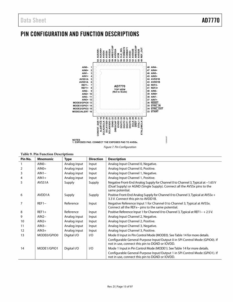
PIN CONFIGURATION AND FUNCTION DESCRIPTIONS
AD7770TOP VIEW
(Not to Scale)
17 18 19 20 21 22 23 24 25 26 27 28 29 30 31 32
CO
NVS
T_SA
RA
LER
T/C
SD
CLK
2/SC
LKD
CLK
1/SD
ID
CLK
0/SD
OD
GN
DD
REG
CA
PIO
VDD
DO
UT3
DO
UT2
DO
UT1
DO
UT0
DC
LKD
RD
YXT
AL1
XTA
L2/M
CLK
64 63 62 61 60 59 58 57 56 55 54 53 52 51 50 49
AU
XAIN
–A
UXA
IN+
AVD
D4
AVS
S4A
VSS2
AA
REG
1CA
PA
VDD
2AVC
MC
LK_S
ELFO
RM
AT0
FOR
MA
T1A
VSS3
AVD
D2B
AR
EG2C
AP
AVS
S2B
REF
_OU
T
123456789
10111213141516
AIN0–AIN0+AIN1–AIN1+
AVSS1AAVDD1A
REF1–REF1+AIN2–AIN2+AIN3–AIN3+
MODE0/GPIO0MODE1/GPIO1MODE2/GPIO2MODE3/ALERT
NOTES1. EXPOSED PAD. CONNECT THE EXPOSED PAD TO AVSSx.
AIN4–AIN4+AIN5–AIN5+AVSS1BAVDD1BREF2–REF2+AIN6–AIN6+AIN7–AIN7+RESETSYNC_INSYNC_OUTSTART
48474645444342414039383736353433
1253
8-00
7
Figure 7. Pin Configuration
Table 9. Pin Function Descriptions Pin No. Mnemonic Type Direction Description 1 AIN0− Analog input Input Analog Input Channel 0, Negative. 2 AIN0+ Analog input Input Analog Input Channel 0, Positive. 3 AIN1− Analog input Input Analog Input Channel 1, Negative. 4 AIN1+ Analog input Input Analog Input Channel 1, Positive. 5 AVSS1A Supply Supply Negative Front-End Analog Supply for Channel 0 to Channel 3, Typical at −1.65 V
(Dual Supply) or AGND (Single Supply). Connect all the AVSSx pins to the same potential.
6 AVDD1A Supply Supply Positive Front-End Analog Supply for Channel 0 to Channel 3, Typical at AVSSx + 3.3 V. Connect this pin to AVDD1B.
7 REF1− Reference Input Negative Reference Input 1 for Channel 0 to Channel 3, Typical at AVSSx. Connect all the REFx− pins to the same potential.
8 REF1+ Reference Input Positive Reference Input 1 for Channel 0 to Channel 3, Typical at REF1− + 2.5 V. 9 AIN2− Analog input Input Analog Input Channel 2, Negative. 10 AIN2+ Analog input Input Analog Input Channel 2, Positive. 11 AIN3− Analog input Input Analog Input Channel 3, Negative. 12 AIN3+ Analog input Input Analog Input Channel 3, Positive. 13 MODE0/GPIO0 Digital I/O I/O Mode 0 Input in Pin Control Mode (MODE0). See Table 14 for more details. Configurable General-Purpose Input/Output 0 in SPI Control Mode (GPIO0). If
not in use, connect this pin to DGND or IOVDD. 14 MODE1/GPIO1 Digital I/O I/O Mode 1 Input in Pin Control Mode (MODE1). See Table 14 for more details. Configurable General-Purpose Input/Output 1 in SPI Control Mode (GPIO1). If
not in use, connect this pin to DGND or IOVDD.
AD7770 Data Sheet
Rev. D | Page 16 of 97
Pin No. Mnemonic Type Direction Description 15 MODE2/GPIO2 Digital I/O I/O Mode 2 Input in Pin Control Mode (MODE2). See Table 14 for more details. Configurable General-Purpose Input/Output 2 in SPI Control Mode (GPIO2). If
not in use, connect this pin to DGND or IOVDD. 16 MODE3/ALERT Digital I/O I/O Mode 3 Input in Pin Control Mode (MODE3). See Table 14 for more details. Alert Output in SPI Control Mode (ALERT). 17 CONVST_SAR Digital input Input Σ-Δ Output Interface Selection Pin in Pin Control Mode. See Table 13 for more
details. This pin also functions as the start for the SAR conversion in SPI control mode.
18 ALERT/CS Digital input Input Alert Output in Pin Control Mode (ALERT).
Chip Select in SPI Control Mode (CS).
19 DCLK2/SCLK Digital input Input DCLK Frequency Selection Pin 2 in Pin Control Mode (DCLK2). See Table 15 for more details.
SPI Clock in SPI Control Mode (SCLK). 20 DCLK1/SDI Digital input Input DCLK Frequency Selection Pin 1 in Pin Control Mode (DCLK1). See Table 15 for
more details. SPI Data Input in SPI Control Mode (SDI). Connect this pin to DGND if the
device is configured in pin control mode with the SPI as the data output interface. 21 DCLK0/SDO Digital output Output DCLK Frequency Selection Pin 0 in Pin Control Mode (DCLK0). See Table 15 for
more details. SPI Data Output in SPI Control Mode (SDO). 22 DGND Supply Supply Digital Ground. 23 DREGCAP Supply Output Digital Low Dropout (LDO) Output. Decouple this pin to DGND with a 1 µF
capacitor. 24 IOVDD Supply Supply Digital Levels Input/Output and Digital LDO (DLDO) Supply from 1.8 V to 3.6 V.
IOVDD must not be lower than DREGCAP. 25 DOUT3 Digital output I/O Data Output Pin 3. If the device is configured in daisy-chain mode, this pin
acts as an input pin. See the Daisy-Chain Mode section for more details. 26 DOUT2 Digital output I/O Data Output Pin 2. If the device is configured in daisy-chain mode, this pin
acts as an input pin. See the Daisy-Chain Mode section for more details. 27 DOUT1 Digital output Output Data Output Pin 1. 28 DOUT0 Digital output Output Data Output Pin 0. 29 DCLK Digital output Output Data Output Clock. 30 DRDY Digital output Output Data Output Ready Pin. 31 XTAL1 Clock Input Crystal 1 Input Connection. If CMOS is used as a clock source, tie this pin to
DGND. See Table 12 for more details. 32 XTAL2/MCLK Clock Input Crystal 2 Input Connection (XTAL2). See Table 12 for more details. CMOS Clock (MCLK). See Table 12 for more details. 33 START Digital input Input Synchronization Pulse. This pin internally synchronizes an external START
asynchronous pulse with MCLK. The synchronize signal is shifted out by the SYNC_OUT pin. If not in use, tie this pin to IOVDD. See the Phase Adjustment section and the Digital Reset and Synchronization Pins section for more details.
34 SYNC_OUT Digital output Input Synchronization Signal. This pin generates a synchronous pulse generated and driven by hardware (via the START pin) or by software (GENERAL_USER_ CONFIG_2, Bit 0). If this pin is in use, it must be wired to the SYNC_IN pin. See the Phase Adjustment section and the Digital Reset and Synchronization Pins section for more details.
35 SYNC_IN Digital input Input Reset for the Internal Digital Block and Synchronize for Multiple Devices. See the Digital Reset and Synchronization Pins section for more details.
36 RESET Digital input Input Asynchronous Reset Pin. This pin resets all registers to their default value. It is recommended to generate a pulse on this pin after the device is powered up because a slow slew rate in the supplies may generate an incorrect initialization in the digital block.
37 AIN7+ Analog input Input Analog Input Channel 7, Positive. 38 AIN7− Analog input Input Analog Input Channel 7, Negative. 39 AIN6+ Analog input Input Analog Input Channel 6, Positive. 40 AIN6− Analog input Input Analog Input Channel 6, Negative. 41 REF2+ Reference Input Positive Reference Input 2 for Channel 4 to Channel 7, Typical at REF2− + 2.5 V.

Data Sheet AD7770
Rev. D | Page 17 of 97
Pin No. Mnemonic Type Direction Description 42 REF2− Reference Input Negative Reference Input 2 for Channel 4 to Channel 7, Typical at AVSSx.
Connect all the REFx− pins to the same potential. 43 AVDD1B Supply Supply Positive Front-End Analog Supply for Channel 4 to Channel 7. Connect this pin
to AVDD1A. 44 AVSS1B Supply Supply Negative Front-End Analog Supply for Channel 4 to Channel 7, typical at −1.65 V
(Dual Supply) or AGND (Single Supply). Connect all the AVSSx pins to the same potential.
45 AIN5+ Analog input Input Analog Input Channel 5, Positive. 46 AIN5− Analog input Input Analog Input Channel 5, Negative. 47 AIN4+ Analog input Input Analog Input Channel 4, Positive. 48 AIN4− Analog input Input Analog Input Channel 4, Negative. 49 REF_OUT Reference Output 2.5 V Reference Output. Connect a 100 nF capacitor on this pin if using the
internal reference. 50 AVSS2B Supply Supply Negative Analog Supply. Connect all the AVSSx pins to the same potential. 51 AREG2CAP Supply Output Analog LDO Output 2. Decouple this pin to AVSS2B with a 1 µF capacitor. 52 AVDD2B Supply Supply Positive Analog Supply. Connect this pin to AVDD2A. 53 AVSS3 Supply Supply Negative Analog Ground. Connect all the AVSSx pins to the same potential. 54 FORMAT1 Digital input Input Output Data Frame 1. See Table 13 for more details. 55 FORMAT0 Digital input Input Output Data Frame 0. See Table 13 for more details. 56 CLK_SEL Digital input Input Select Clock Source. See Table 12 for more details. 57 VCM Analog output Output Common-Mode Voltage Output, Typical at (AVDD1 + AVSSx)/2. 58 AVDD2A Supply Input Analog Supply from 2.2 V to 3.6 V. AVSS2x must not be lower than AREGxCAP.
Connect this pin to AVDD2B. 59 AREG1CAP Supply Output Analog LDO Output 1. Decouple this pin to AVSSx with a 1 µF capacitor. 60 AVSS2A Supply Input Negative Analog supply. Connect all the AVSSx pins to the same potential. 61 AVSS4 Supply Supply Negative SAR Analog Supply and Reference. Connect all AVSSx pins to the same
potential. 62 AVDD4 Supply Supply Positive SAR Analog Supply and Reference Source. 63 AUXAIN+ Analog input Input Positive SAR Analog Input Channel. 64 AUXAIN− Analog input Input Negative SAR Analog Input Channel. EPAD Supply Input Exposed Pad. Connect the exposed pad to AVSSx.

AD7770 Data Sheet
Rev. D | Page 18 of 97
TYPICAL PERFORMANCE CHARACTERISTICS
–10
–8
–6
–4
–2
0
2
4
10
8
6
–2.4
8
–2.1
2
–1.7
7
–1.4
1
–1.0
6
–0.7
0
–0.3
5 0
0.35
0.70
1.06
1.41
1.77
2.12
2.48
INL
(ppm
)
INPUT VOLTAGE (V)
TEMPERATURE = 25°CGAIN = 1DIFFERENTIAL INPUT SIGNALVREF = 2.5VVCM = (AVDD1x + AVSSx) ÷ 2
CH 3CH 2CH 1CH 0
CH 4CH 5CH 6CH 7
1253
8-20
8
Figure 8. INL vs. Input Voltage and Channel at 16 kSPS, High Resolution Mode
–10
–8
–6
–4
–2
0
2
4
10
8
6
–2.4
8
–2.1
2
–1.7
7
–1.4
1
–1.0
6
–0.7
0
–0.3
5 0
0.35
0.70
1.06
1.41
1.77
2.12
2.48
INL
(ppm
)
INPUT VOLTAGE (V)
TEMPERATURE = 25°CVREF = 2.5VDIFFERENTIAL VIN × GAINVCM = (AVDD1x + AVSSx) ÷ 2
GAIN = 1GAIN = 2GAIN = 4GAIN = 8
1253
8-20
9
Figure 9. INL vs. Input Voltage and PGA Gain at 16 kSPS, High Resolution Mode
–12
–10
–8
–6
–4
–2
0
2
4
10
8
6
–2.4
8
–2.1
2
–1.7
7
–1.4
1
–1.0
6
–0.7
0
–0.3
5 0
0.35
0.70
1.06
1.41
1.77
2.12
2.48
INL
(ppm
)
INPUT VOLTAGE (V)
GAIN = 1DIFFERENTIAL INPUT SIGNALVREF = 2.5VVCM = (AVDD1x + AVSSx) ÷ 2
TA = –40°CTA = +25CTA = +105°CTA = +125°C
1253
8-21
0
Figure 10. INL vs. Input Voltage and Temperature at 16 kSPS,
High Resolution Mode
–15
–10
–5
0
5
10
15
–2.4
8
–2.1
2
–1.7
7
–1.4
1
–1.0
6
–0.7
0
–0.3
5 0
0.35
0.70
1.06
1.41
1.77
2.12
2.48
INL
(ppm
)
INPUT VOLTAGE (V)
TEMPERATURE = 25°CGAIN = 1DIFFERENTIAL INPUT SIGNALVREF = 2.5VVCM = (AVDD1x + AVSSx) ÷ 2
CH 3CH 2CH 1CH 0
CH 4CH 5CH 6CH 7
1253
8-21
1
Figure 11. INL vs. Input Voltage and Channel at 4 kSPS, Low Power Mode
–15
–10
–5
0
5
10
–2.4
8
–2.1
2
–1.7
7
–1.4
1
–1.0
6
–0.7
0
–0.3
5 0
0.35
0.70
1.06
1.41
1.77
2.12
2.48
INL
(ppm
)
INPUT VOLTAGE (V)
TEMPERATURE = 25°CVREF = 2.5VDIFFERENTIAL VIN × GAINVCM = (AVDD1x + AVSSx) ÷ 2
GAIN = 1GAIN = 2GAIN = 4GAIN = 8
1253
8-21
2
Figure 12. INL vs. Input Voltage and PGA Gain at 4 kSPS, Low Power Mode
–15
–10
–5
0
5
10
15
–2.4
8
–2.1
2
–1.7
7
–1.4
1
–1.0
6
–0.7
0
–0.3
5 0
0.35
0.70
1.06
1.41
1.77
2.12
2.48
INL
(ppm
)
INPUT VOLTAGE (V)
GAIN = 1DIFFERENTIAL INPUT SIGNALVREF = 2.5VVCM = (AVDD1x + AVSSx) ÷ 2
TA = –40°CTA = +25CTA = +105°CTA = +125°C
1253
8-21
3
Figure 13. INL vs. Input Voltage and Temperature at 4 kSPS,
Low Power Mode

Data Sheet AD7770
Rev. D | Page 19 of 97
–20
–15
–10
–5
0
5
10
20
15
–4 –3 –2 –1 0 1 2 3 4
INL
(ppm
)
INPUT VOLTAGE (V)
TEMPERATURE = 25°CGAIN = 1DIFFERENTIAL INPUT SIGNALVCM = (AVDD1x + AVSSx) ÷ 2
VREF = 1VVREF = 1.5VVREF = 2VVREF = 2.5VVREF = 3VVREF = 3.3V
1253
8-21
4
Figure 14. INL vs. Input Voltage and Reference Voltage (VREF)
at 16 kSPS, High Resolution Mode
–10
–6
–2
2
6
–8
–4
0
4
8
10
–2.4
8
–2.1
2
–1.7
7
–1.4
1
–1.0
6
–0.7
0
–0.3
5 0
0.35
0.70
1.06
1.41
1.77
2.12
2.48
INL
(ppm
)
INPUT VOLTAGE (V)
TEMPERATURE = 25°CVREF = 2.5VDIFFERENTIAL INPUT SIGNALGAIN = 1
VCM = 1.35VVCM = 1.65VVCM = 1.95V
1253
8-21
5
Figure 15. INL vs. Input Voltage and VCM at 16 kSPS, High Resolution Mode
0
200
400
600
800
1000
1200
1400
SAM
PLE
CO
UN
T
ADC CODE
VREF = 2.5VVCM = (AVDD1x + AVSSx) ÷ 2TEMPERATURE = 25°C
8388
212
8388
256
8388
300
8388
344
8388
388
8388
432
8388
476
8388
520
8388
564
8388
608
8388
652
GAIN = 1GAIN = 2GAIN = 4GAIN = 8
1253
8-21
6
Figure 16. Noise Histogram at 16 kSPS, High Resolution Mode
–20
–15
–10
–5
0
5
10
20
15
–4 –3 –2 –1 0 1 2 3 4
INL
(ppm
)
INPUT VOLTAGE (V)
TEMPERATURE = 25°CGAIN = 1DIFFERENTIAL INPUT SIGNALVCM = (AVDD1x + AVSSx) ÷ 2
VREF = 1VVREF = 1.5VVREF = 2VVREF = 2.5VVREF = 3VVREF = 3.3V
1253
8-21
7
Figure 17. INL vs. Input Voltage and VREF at 4 kSPS, Low Power Mode
–15
–5
5
–10
0
10
15
–2.4
8
–2.1
2
–1.7
7
–1.4
1
–1.0
6
–0.7
0
–0.3
5 0
0.35
0.70
1.06
1.41
1.77
2.12
2.48
INL
(ppm
)
INPUT VOLTAGE (V)
TEMPERATURE = 25°CVREF = 2.5VDIFFERENTIAL INPUT SIGNALGAIN =1
VCM = 1.35VVCM = 1.65VVCM = 1.95V
1253
8-21
8
Figure 18. INL vs. Input Voltage and VCM at 4 kSPS, Low Power Mode
0
200
400
600
800
1000
1200
1400
SAM
PLE
CO
UN
T
ADC CODE
VREF = 2.5VVCM = (AVDD1x + AVSSx) ÷ 2TEMPERATURE = 25°C
GAIN = 1GAIN = 2GAIN = 4GAIN = 8
8388
164
8388
204
8388
244
8388
284
8388
324
8388
364
8388
404
8388
444
8388
484
8388
524
8388
564
8388
604
8388
644
1253
8-21
9
Figure 19. Noise Histogram at 4 kSPS, Low Power Mode

AD7770 Data Sheet
Rev. D | Page 20 of 97
0
1
–40 25 105 125
2
3
4
5
6
7
8
NOIS
E (µ
V rm
s)
TEMPERATURE (°C)
VREF = 2.5VVCM = (AVDD1x + AVSSx) ÷ 2
GAIN = 1GAIN = 2GAIN = 4GAIN = 8
1253
8-22
0
Figure 20. Noise vs. Temperature at 16 kSPS, High Resolution Mode
3353
6065
2800
9702
4012
8768
016
0512
019
2256
022
4000
025
5744
028
7488
031
9232
035
0976
038
2720
041
4464
044
6208
047
7952
050
9696
054
1440
057
3184
060
4928
063
6672
066
8416
070
0160
073
1904
076
3648
079
5392
00
1
2
3
4
5
6
7
NO
ISE
(µV
rms)
CLOCK FREQUENCY (Hz)
VREF = 2.5VVCM = (AVDD1x + AVSSx) ÷ 2TEMPERATURE = 25°CDECIMATION = 256
GAIN = 1GAIN = 2GAIN = 4GAIN = 8
1253
8-22
1
Figure 21. Noise vs. Clock Frequency, High Resolution Mode
0
20
40
60
80
100
120
140
NO
ISE
(nV/
√Hz)
ODR (SPS)2000 4000 8000 16000 32000
GAIN = 1GAIN = 2GAIN = 4GAIN = 8
1253
8-22
2
Figure 22. Noise vs. ODR, High Resolution Mode
0
1
–40 25 105 125
2
3
4
5
6
7
8
NOIS
E (µ
V rm
s)
TEMPERATURE (°C)
VREF = 2.5VVCM = (AVDD1x + AVSSx) ÷ 2
GAIN = 1GAIN = 2GAIN = 4GAIN = 8
1253
8-22
3
Figure 23. Noise vs. Temperature at 4 kSPS, Low Power Mode
0
1
2
3
4
5
6
7
NO
ISE
(µV
rms)
CLOCK FREQUENCY (Hz)
VREF = 2.5VVCM = (AVDD1x + AVSSx) ÷ 2TEMPERATURE = 25°CDECIMATION = 256
GAIN = 1GAIN = 2GAIN = 4GAIN = 8
2944
0044
8000
6016
0075
5200
9088
0010
6240
012
1600
013
6960
015
2320
016
7680
018
3040
019
8400
021
3760
022
9120
024
4480
025
9840
027
5200
029
0560
030
5920
032
1280
033
6640
035
2000
036
7360
038
2720
039
8080
0
1253
8-22
4
Figure 24. Noise vs. Clock Frequency, Low Power Mode
0
50
100
150
200
250
300
NO
ISE
(nV/
√Hz)
ODR (SPS)500 1000 2000 4000 8000
GAIN = 1GAIN = 2GAIN = 4GAIN = 8
1253
8-22
5
Figure 25. Noise vs. ODR, Low Power Mode

Data Sheet AD7770
Rev. D | Page 21 of 97
AM
PLIT
UD
E (d
B)
FREQUENCY (Hz)
–180–170–160–150–140–130–120–110–100
–90–80–70–60–50–40–30–20–10
010
065
6.25
0000
1296
.875
000
1986
.328
125
2617
.187
500
3250
.000
000
3884
.765
625
4156
.250
000
4789
.062
500
5427
.734
375
6066
.406
250
6703
.125
000
7312
.500
000
7921
.875
000
8531
.250
000
9140
.625
000
9750
.000
000
1035
9.37
5000
1096
8.75
0000
1157
8.12
5000
1218
7.50
0000
1279
6.87
5000
1340
6.25
0000
1401
5.62
5000
1462
5.00
0000
1523
4.37
5000
1584
3.75
0000
GAIN = 1GAIN = 2GAIN = 4GAIN = 8
VREF = 2.5VTEMPERATURE = 25°CDIFFERENTIAL INPUT = –0.5dBFSVCM = (AVDD1x + AVSSx) ÷ 2INPUT FREQUENCY = 50Hz16384 SAMPLES32kSPS
1253
8-22
6
Figure 26. FFT at 32 kSPS, High Resolution Mode, Input Frequency (fIN) = 50 Hz
AM
PLIT
UD
E (d
B)
FREQUENCY (Hz)
–180–170–160–150–140–130–120–110–100
–90–80–70–60–50–40–30–20–10
010
GAIN = 1GAIN = 2GAIN = 4GAIN = 8
VREF = 2.5VTEMPERATURE = 25°CDIFFERENTIAL INPUT = –0.5dBFSVCM = (AVDD1x + AVSSx) ÷ 2INPUT FREQUENCY = 1kHz16384 SAMPLES32kSPS
0
1103
.515
625
2234
.375
000
3304
.687
500
4388
.671
875
5462
.890
625
6533
.203
125
7648
.437
500
8562
.500
000
9632
.812
500
1070
3.12
5000
1177
3.43
7500
1284
3.75
0000
1391
4.06
2500
1498
4.37
5000
1253
8-22
7
Figure 27. FFT at 32 kSPS, High Resolution Mode,
Input Frequency (fIN) = 1 kHz
–130
–125
–120
–115
–110
–105
–100
THD
(dB
)
INPUT FREQUENCY (Hz)
VIN = –0.5dBFSVREF = 2.5VTEMPERATURE = 25°C
GAIN = 1GAIN = 2GAIN = 4GAIN = 8
10 109
208
307
406
505
604
703
802
901
1000
1700
2400
3170
3870
4710
5620
6320
7160
7860
1253
8-22
8
Figure 28. THD vs. Input Frequency at 16 kSPS, High Resolution Mode
AM
PLIT
UD
E (d
B)
FREQUENCY (Hz)
–180–170–160–150–140–130–120–110–100
–90–80–70–60–50–40–30–20–10
010
GAIN = 1GAIN = 2GAIN = 4GAIN = 8
VREF = 2.5VTEMPERATURE = 25°CDIFFERENTIAL INPUT = –0.5dBFSVCM = (AVDD1x + AVSSx) ÷ 2INPUT FREQUENCY = 50Hz8192 SAMPLES8kSPS
0
261.
7187
5
523.
4375
0
785.
1562
5
1046
.875
00
1308
.593
75
1570
.312
50
1832
.031
25
2093
.750
00
2355
.468
75
2617
.187
50
2878
.906
25
3140
.625
00
3402
.343
75
3664
.062
50
3925
.781
25
1253
8-22
9
Figure 29. FFT at 8 kSPS, Low Power Mode, Input Frequency (fIN) = 50 Hz
AM
PLIT
UD
E (d
B)
FREQUENCY (Hz)
–180–170–160–150–140–130–120–110–100
–90–80–70–60–50–40–30–20–10
010
GAIN = 1GAIN = 2GAIN = 4GAIN = 8
VREF = 2.5VTEMPERATURE = 25°CDIFFERENTIAL INPUT = –0.5dBFSVCM = (AVDD1x + AVSSx) ÷ 2INPUT FREQUENCY = 1kHz8192 SAMPLES8kSPS
0
273.
4375
546.
8750
820.
3125
1093
.750
0
1367
.187
5
1640
.625
0
1914
.062
5
2187
.500
0
2460
.937
5
2734
.375
0
3007
.812
5
3281
.250
0
3554
.687
5
3828
.125
0
1253
8-23
0
Figure 30. FFT at 8 kSPS, Low Power Mode, Input Frequency (fIN) = 1 kHz
–130
–125
–120
–115
–110
–105
–100
THD
(dB
)
INPUT FREQUENCY (Hz)
VIN = –0.5dBFSVREF = 2.5VTEMPERATURE = 25°C
GAIN = 1GAIN = 2GAIN = 4GAIN = 8
10.0
208.
0
406.
0
604.
0
811.
9
1 010
.0
1220
.0
1440
.0
1660
.0
1870
.0
1253
8-23
1
Figure 31. THD vs. Input Frequency at 4 kSPS, Low Power Mode

AD7770 Data Sheet
Rev. D | Page 22 of 97
–140
–135
–130
–125
–120
–115
–110
–105
–100
THD
(dB
)
INPUT VOLTAGE (V)
INPUT FREQUENCY = 50HzVREF = 2.5VTEMPERATURE = 25°C
GAIN = 1GAIN = 2GAIN = 4GAIN = 8
0.17
20.
344
0.51
60.
688
0.86
01.
032
1.20
41.
376
1.54
81.
720
1.89
22.
064
2.23
62.
408
2.58
02.
752
2.92
43.
096
3.26
83.
440
3.61
23.
784
3.95
64.
128
4.30
04.
472
4.64
4
1253
8-23
2
Figure 32. THD vs. Input Voltage at 16 kSPS, High Resolution Mode
–125
–120
–115
–110
–105
–100
–95
–90
THD
(dB
)
REFERENCE VOLTAGE (V)
INPUT FREQUENCY = 50HzINPUT VOLTAGE = –0.5dBFSTEMPERATURE = 25°C
GAIN = 1GAIN = 2GAIN = 4GAIN = 8
0.2 0.4 0.6 0.8 1.0 1.2 1.4 1.6 1.8 2.0 2.2 2.4 2.6 2.8 3.0 3.2
1253
8-23
3
Figure 33. THD vs. Reference Voltage at 16 kSPS, High Resolution Mode
–125
–120
–115
–110
–105
–100
THD
(dB
)
MCLK FREQUENCY (Hz)
3353
60
9702
40
1605
120
2240
000
2874
880
3509
760
4144
640
4779
520
5414
400
6049
280
6684
160
7319
040
7953
920
GAIN = 1GAIN = 2GAIN = 4GAIN = 8
INPUT FREQUENCY = 50HzVREF = 2.5VINPUT VOLTAGE = –0.5dBFSTEMPERATURE = 25°CDECIMATION = 256
1253
8-23
4
Figure 34. THD vs. MCLK Frequency, High Resolution Mode
–140
–135
–130
–125
–120
–115
–110
–105
–100
THD
(dB
)
INPUT VOLTAGE (V)
INPUT FREQUENCY = 50HzVREF = 2.5VTEMPERATURE = 25°C
GAIN = 1GAIN = 2GAIN = 4GAIN = 8
0.17
20.
344
0.51
60.
688
0.86
01.
032
1.20
41.
376
1.54
81.
720
1.89
22.
064
2.23
62.
408
2.58
02.
752
2.92
43.
096
3.26
83.
440
3.61
23.
784
3.95
64.
128
4.30
04.
472
4.64
4
1253
8-23
5
Figure 35. THD vs. Input Voltage at 4 kSPS, Low Power Mode
–125
–120
–115
–110
–105
–100
–95
–90
THD
(dB
)
REFERENCE VOLTAGE (V)
INPUT FREQUENCY = 50HzINPUT VOLTAGE = –0.5dBFSTEMPERATURE = 25°C
GAIN = 1GAIN = 2GAIN = 4GAIN = 8
0.2 0.4 0.6 0.8 1.0 1.2 1.4 1.6 1.8 2.0 2.2 2.4 2.6 2.8 3.0 3.2
1253
8-23
6
Figure 36. THD vs. Reference Voltage at 4 kSPS, Low Power Mode
–130
–125
–120
–115
–110
–105
–100
THD
(dB
)
MCLK FREQUENCY (Hz)
GAIN = 1GAIN = 2GAIN = 4GAIN = 8
INPUT FREQUENCY = 50HzVREF = 2.5VINPUT VOLTAGE = –0.5dBFSTEMPERATURE = 25°CDECIMATION = 256
1676
80
4851
20
8025
60
1120
000
1437
440
1754
880
2072
320
2389
760
2707
200
3024
640
3342
080
3659
520
3976
960
1253
8-23
7
Figure 37. THD vs. MCLK Frequency, Low Power Mode
Data Sheet AD7770
Rev. D | Page 23 of 97
85
125
120
115
110
105
100
95
90
SNR
(dB)
ODR (kHz)
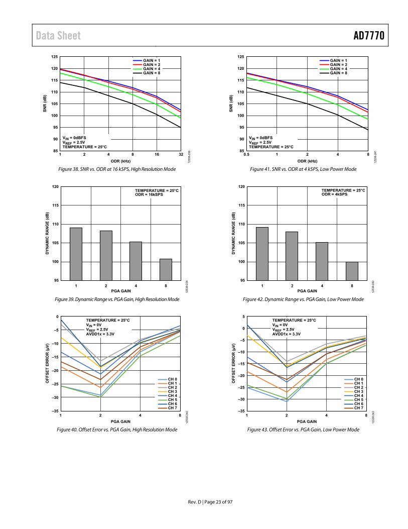
VIN = 0dBFSVREF = 2.5VTEMPERATURE = 25°C
GAIN = 1GAIN = 2GAIN = 4GAIN = 8
1 3216842
1253
8-23
8
Figure 38. SNR vs. ODR at 16 kSPS, High Resolution Mode
95
100
105
110
115
120
DYNA
MIC
RAN
GE
(dB)
PGA GAIN1 2 4 8
TEMPERATURE = 25°CODR = 16kSPS
1253
8-23
9
Figure 39. Dynamic Range vs. PGA Gain, High Resolution Mode
–35
–25
–30
–20
–15
–10
–5
0
1 2 4 8
OFF
SET
ERR
OR
(µV)
PGA GAIN
CH 0CH 1CH 2CH 3CH 4CH 5CH 6CH 7
TEMPERATURE = 25°CVIN = 0VVREF = 2.5VAVDD1x = 3.3V
1253
8-24
0
Figure 40. Offset Error vs. PGA Gain, High Resolution Mode
85
125
120
115
110
105
100
95
90
SNR
(dB)
ODR (kHz)
VIN = 0dBFSVREF = 2.5VTEMPERATURE = 25°C
GAIN = 1GAIN = 2GAIN = 4GAIN = 8
0.5 8421
1253
8-24
1
Figure 41. SNR vs. ODR at 4 kSPS, Low Power Mode
95
100
105
110
115
120
DYNA
MIC
RAN
GE
(dB)
PGA GAIN1 2 4 8
TEMPERATURE = 25°CODR = 4kSPS
1253
8-24
2
Figure 42. Dynamic Range vs. PGA Gain, Low Power Mode
–35
–25
–30
–20
–15
–10
–5
5
0
1 2 4 8
OFF
SET
ERR
OR
(µV)
PGA GAIN
CH 0CH 1CH 2CH 3CH 4CH 5CH 6CH 7
TEMPERATURE = 25°CVIN = 0VVREF = 2.5VAVDD1x = 3.3V
1253
8-24
3
Figure 43. Offset Error vs. PGA Gain, Low Power Mode

AD7770 Data Sheet
Rev. D | Page 24 of 97
–18
–16
–14
–12
–10
–8
–6
–4
–2
0
OFF
SET
ERRO
R (µ
V)
POWER SUPPLY SETTING
TEMPERATURE = 25°CVIN = 0VVREF = 2.5V
GAIN = 1GAIN = 2GAIN = 4GAIN = 8
3.0 3.63.3
1253
8-24
4
Figure 44. Offset Error vs. Power Supply Setting, High Resolution Mode
–50
40
30
20
10
0
–10
–20
–30
–40
–40 –20 0 20 40 60 80 100 120
OFF
SET
DR
IFT
(µV)
TEMPERATURE (°C)
CH 0CH 1CH 2CH 3CH 4CH 5CH 6CH 7
AVDD1x = 3.3V
1253
8-24
5
Figure 45. Offset Drift vs. Temperature
–0.043
–0.035
–0.026
–0.017
–0.008
0
0.008
0.017
3.0 3.3 3.6
GA
IN E
RR
OR
(%)
AVDD1x SUPPLY (V)
CH 0CH 1CH 2CH 3CH 4CH 5CH 6CH 7
1253
8-24
6
TEMPERATURE = 25°CGAIN = 1VREF = 2.5VVIN = 0dBFS
Figure 46. Gain Error vs. AVDD1x Supply, High Resolution Mode
–16
–14
–12
–10
–8
–6
–4
–2
4
2
0
OFF
SET
ERRO
R (µ
V)
POWER SUPPLY SETTING
TEMPERATURE = 25°CVIN = 0VVREF = 2.5V
GAIN = 1GAIN = 2GAIN = 4GAIN = 8
3.0 3.63.3
1253
8-24
7
Figure 47. Offset Error vs. Power Supply Setting, Low Power Mode
1253
8-24
8–20
–15
–10
–5
0
5
10
15
20
25
30
45
40
35
0 500168 1000
GA
IN E
RR
OR
DR
IFT
(ppm
)
TIME (Hours) Figure 48. Gain Error Drift vs. Time
3.0 3.3 3.6
AVDD1x SUPPLY (V)
TEMPERATURE = 25°CGAIN = 1VREF = 2.5VVIN = 0dBFS
GA
IN E
RR
OR
(%)
–0.043
–0.035
–0.026
–0.017
–0.008
0
0.008
0.017CH 0CH 1CH 2CH 3CH 4CH 5CH 6CH 7
1253
8-24
9
Figure 49. Gain Error vs. AVDD1x Supply, Low Power Mode

Data Sheet AD7770
Rev. D | Page 25 of 97
–40 25 105 125
GAI
N ER
ROR
(%)
TEMPERATURE (°C)
AVDD1x = 3.3VVREF = 2.5VVIN = 0dBFS
–0.400
–0.035
–0.029
–0.023
–0.017
–0.011
–0.005
0
0.005
0.011
0.017CH 0CH 1CH 2CH 3CH 4CH 5CH 6CH 7
1253
8-25
0
Figure 50. Gain Error vs. Temperature, High Resolution Mode
0
0.01
0.02
0.03
0.04
0.05
0.06
0.07
0.08
0.09
1 2 4 8
GAI
N ER
ROR
(%)
PGA GAIN
HIGH RESOLUTIONLOW POWER
TEMPERATURE = 25°CAVDD1x = 3.3VVREF = 2.5VVIN = 0dBFS
1253
8-25
1
Figure 51. Channel Gain Mismatch, High Resolution Mode
–40 25 105 125
TUE
(% O
F IN
PUT)
TEMPERATURE (°C)
–0.030
–0.025
–0.020
–0.015
–0.010
–0.005
0
0.005
CH 0CH 1CH 2CH 3CH 4CH 5CH 6CH 7
TEMPERATURE = 25°CVIN = –0.5dBFSVREF = 2.5VAVDD1x = 3.3VGAIN = 1
1253
8-25
2
Figure 52. Total Unadjusted Error (TUE) vs. Temperature,
High Resolution Mode
–0.400
–0.035
–0.029
–0.023
–0.017
–0.011
–0.005
0
0.005
0.011
0.017
–40 25 105 125
GAI
N ER
ROR
(%)
TEMPERATURE (°C)
AVDD1x = 3.3VVREF = 2.5VVIN = 0dBFS
CH 0CH 1CH 2CH 3CH 4CH 5CH 6CH 7
1253
8-25
3
Figure 53. Gain Error vs. Temperature, Low Power Mode
–40 25 105 125
REFE
RENC
E VO
LTAG
E DR
IFT
(mV)
TEMPERATURE (°C)
–6
4
3
2
1
0
–1
–2
–3
–4
–5
1253
8-25
4
Figure 54. Internal Reference Voltage Drift
–40 25 105 125
TUE
(% O
F IN
PUT)
TEMPERATURE (°C)
–0.015
0
–0.005
–0.010
0.005
0.010
CH 0CH 1CH 2CH 3CH 4CH 5CH 6CH 7
TEMPERATURE = 25°CVIN = –0.5dBFSVREF = 2.5VAVDD1x = 3.3VGAIN = 1
1253
8-25
5
Figure 55. Total Unadjusted Error (TUE) vs. Temperature, Low Power Mode

AD7770 Data Sheet
Rev. D | Page 26 of 97
–4
–3
–2
–1
0
1
2
3
4
–2.5 –2.0 –1.5 –1.0 –0.5 0 0.5 1.0 1.5 2.0 2.5
INPU
T C
UR
REN
T (n
A)
DIFFERENTIAL INPUT VOLTAGE ((AINx+) – (AINx–))
AINx+; VCM = 1.95VAINx–; VCM = 1.95VAINx+; VCM = 1.35VAINx–; VCM = 1.35V
VREF = 2.5VAVDD1x = 3.3V
1253
8-25
6
Figure 56. Input Current vs. Differential Input Voltage, High Resolution Mode
–40 25 105 125
AB
SOLU
TE IN
PUT
CU
RR
ENT
(nA
)
TEMPERATURE (°C)
VREF = 2.5VVIN = 2.5VAVDD1x = 3.3V
–12
–10
–8
–6
–4
–2
0
2
4
6
AIN0+AIN0–AIN2+AIN2–
1253
8-25
7
Figure 57. Absolute Input Current vs. Temperature, High Resolution Mode
–2.5 –2.0 –1.5 –1.0 –0.5 0 0.5 1.0 1.5 2.52.0
DIF
FER
ENTI
AL
INPU
T C
UR
REN
T (n
A)
DIFFERENTIAL INPUT VOLTAGE ((AINx+) – (AINx–))
–5
–4
–3
–2
–1
0
1
2
3
4
5AINx+ – AINx–; VCM = 1.95VAINx+ – AINx–; VCM = 1.35V
VREF = 2.5VAVDD1x = 3.3V
1253
8-25
8
Figure 58. Differential Input Current vs. Differential Input Voltage,
High Resolution Mode
–1.0
–0.8
–0.6
–0.4
–0.2
0
0.2
0.4
0.6
0.8
1.0
–2.5 –2.0 –1.5 –1.0 –0.5 0 0.5 1.0 1.5 2.0 2.5
INPU
T C
UR
REN
T (n
A)
DIFFERENTIAL INPUT VOLTAGE ((AINx+) – (AINx–))
AINx+; VCM = 1.95VAINx–; VCM = 1.95VAINx+; VCM = 1.35VAINx–; VCM = 1.35V
VREF = 2.5VAVDD1x = 3.3V
1253
8-25
9
Figure 59. Input Current vs. Differential Input Voltage, Low Power Mode
–40 25 105 125
AB
SOLU
TE IN
PUT
CU
RR
ENT
(nA
)
TEMPERATURE (°C)
VREF = 2.5VVIN = 2.5VAVDD1x = 3.3V
–6
–5
–4
–3
–2
–1
0
1
3
2
4
AIN0+AIN0–AIN2+AIN2–
1253
8-26
0
Figure 60. Absolute Input Current vs. Temperature, Low Power Mode
–2.5 –2.0 –1.5 –1.0 –0.5 0 0.5 1.0 1.5 2.52.0
DIF
FER
ENTI
AL
INPU
T C
UR
REN
T (n
A)
DIFFERENTIAL INPUT VOLTAGE ((AINx+) – (AINx–))
–1
–0.8
–0.6
–0.4
–0.2
0
0.2
0.4
0.6
1.0
0.8
1.2AINx+ – AINx–; VCM = 1.95VAINx+ – AINx–; VCM = 1.35V
VREF = 2.5VAVDD1x = 3.3V
1253
8-26
1
Figure 61. Differential Input Current vs. Differential Input Voltage,
Low Power Mode

Data Sheet AD7770
Rev. D | Page 27 of 97
25 105 125
DIFF
EREN
TIAL
INPU
T CU
RREN
T (n
A)
TEMPERATURE (°C)
VREF = 2.5VVIN = 2.5VAVDD1x = 3.3V
CH 0CH 1CH 2CH 3CH 4CH 5CH 6CH 7
1253
8-26
2
Figure 62. Differential Input Current vs. Temperature, High Resolution Mode
–140
–120
–100
–80
–60
–40
–20
0
CMRR
(dB)
INPUT FREQUENCY (Hz)
250.
1387
35
1321
3.72
3000
2617
7.30
7000
3961
5.16
9000
5257
8.75
3000
6617
4.70
7000
7913
8.29
1000
9210
1.87
5000
1056
97.8
3000
0
1186
61.4
1400
0
1321
78.3
2200
0
1451
41.9
0600
0
1581
05.4
9000
0
1715
43.3
5200
0
1845
06.9
3600
0
1980
23.8
4400
0
GAIN = 1GAIN = 2GAIN = 4GAIN = 8
AVDD1x = 3.3VVCM = 1.65V + 100mV p-p
1253
8-26
3
Figure 63. Common-Mode Rejection Ratio (CMRR) vs. Input Frequency at
16 kSPS, High Resolution Mode
–160–150–140–130–120–110–100
–90–80–70–60–50–40–30–20–10
0
AC
PSR
R (d
B)
INPUT FREQUENCY (Hz)
GAIN = 1GAIN = 2GAIN = 4GAIN = 8
AVDD1x = 3.3V + 100mV p-pTEMPERATURE = 25°C
2001
4.97
5800
14.1
3
1140
013.
00
1680
012.
00
2220
012.
00
2780
011.
00
3320
010.
00
3880
009.
00
4500
008.
00
5040
007.
00
5580
007.
00
6140
006.
00
6680
005.
00
7240
004.
00
7780
003.
00
8360
002.
00
8900
002.
00
9460
001.
00
1253
8-26
4
Figure 64. AC Power Supply Rejection Ratio (PSRR) vs. Input Frequency at
16 kSPS, High Resolution Mode
–40 25 105 125
DIFF
EREN
TIAL
INPU
T CU
RREN
T (n
A)
TEMPERATURE (°C)
VREF = 2.5VVIN = 2.5VAVDD1x = 3.3V
0
1
2
3
4
5
6
7
8CH 0CH 1CH 2CH 3CH 4CH 5CH 6CH 7
1253
8-26
5
Figure 65. Differential Input Current vs. Temperature, Low Power Mode
171.
0924
9
1345
0.86
2
2688
8.72
3
4064
2.77
5392
2.53
9
6736
0.40
1
8111
4.44
7
9455
2.30
9
1079
90.1
71
1215
86.1
25
1350
23.9
87
1484
61.8
48
1622
15.8
95
1756
53.7
57
1889
33.5
26
–140
–120
–100
–80
–60
–40
–20
0
CMRR
(dB)
INPUT FREQUENCY (Hz)
GAIN = 1GAIN = 2GAIN = 4GAIN = 8
AVDD1x = 3.3VVCM = 1.65V + 100mV p-p
1253
8-26
6
Figure 66. CMRR vs. Input Frequency at 4 kSPS, Low Power Mode
–160–150–140–130–120–110–100
–90–80–70–60–50–40–30–20–10
0
AC
PSR
R (d
B)
INPUT FREQUENCY (Hz)
GAIN = 1GAIN = 2GAIN = 4GAIN = 8
AVDD1x = 3.3V + 100mV p-pTEMPERATURE = 25°C
2001
4.97
5800
14.1
3
1140
013.
00
1680
012.
00
2220
012.
00
2780
011.
00
3320
010.
00
3880
009.
00
4500
008.
00
5040
007.
00
5580
007.
00
6140
006.
00
6680
005.
00
7240
004.
00
7780
003.
00
8360
002.
00
8900
002.
00
9460
001.
00
1253
8-26
7
Figure 67. AC PSRR vs. Input Frequency at 4 kSPS, Low Power Mode
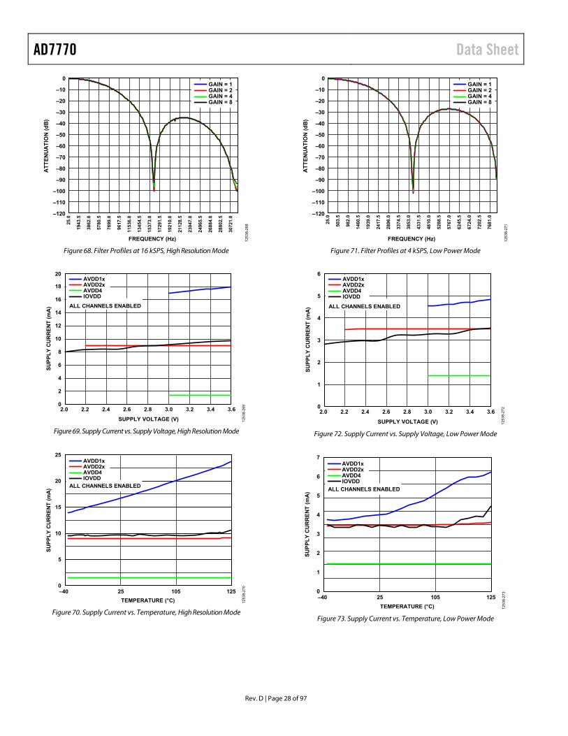
AD7770 Data Sheet
Rev. D | Page 28 of 97
–120
–110
–100
–90
–80
–70
–60
–50
–40
–30
–20
–10
0
ATT
ENU
ATI
ON
(dB
)
FREQUENCY (Hz)
GAIN = 1GAIN = 2GAIN = 4GAIN = 8
25.0
1943
.5
3862
.0
5780
.5
7699
.0
9617
.5
1153
6.0
1345
4.5
1537
3.0
1729
1.5
1921
0.0
2112
8.5
2304
7.0
2496
5.5
2688
4.0
2880
2.5
3072
1.0
1253
8-26
8
Figure 68. Filter Profiles at 16 kSPS, High Resolution Mode
0
2
4
6
8
10
12
14
16
18
20
2.0 2.2 2.4 2.6 2.8 3.0 3.2 3.4 3.6
SUPP
LY C
URRE
NT (m
A)
SUPPLY VOLTAGE (V)
ALL CHANNELS ENABLED
AVDD1xAVDD2xAVDD4IOVDD
1253
8-26
9
Figure 69. Supply Current vs. Supply Voltage, High Resolution Mode
–40 25 105 1250
25
20
15
10
5
SUPP
LY C
URRE
NT (m
A)
TEMPERATURE (°C)
ALL CHANNELS ENABLED
AVDD1xAVDD2xAVDD4IOVDD
1253
8-27
0
Figure 70. Supply Current vs. Temperature, High Resolution Mode
–120
–110
–100
–90
–80
–70
–60
–50
–40
–30
–20
–10
0
ATT
ENU
ATI
ON
(dB
)
FREQUENCY (Hz)
GAIN = 1GAIN = 2GAIN = 4GAIN = 8
25.0
503.
5
982.
0
1460
.5
1939
.0
2417
.5
2896
.0
3374
.5
3853
.0
4331
.5
4810
.0
5288
.5
5767
.0
6245
.5
6724
.0
7202
.5
7681
.0
1253
8-27
1
Figure 71. Filter Profiles at 4 kSPS, Low Power Mode
0
6
5
4
3
2
1
2.0 2.2 2.4 2.6 2.8 3.0 3.2 3.4 3.6
SUPP
LY C
UR
REN
T (m
A)
SUPPLY VOLTAGE (V)
ALL CHANNELS ENABLED
AVDD1xAVDD2xAVDD4IOVDD
1253
8-27
2
Figure 72. Supply Current vs. Supply Voltage, Low Power Mode
–40 25 105 1250
7
6
5
4
3
2
1
SUPP
LY C
UR
REN
T (m
A)
TEMPERATURE (°C)
ALL CHANNELS ENABLED
AVDD1xAVDD2xAVDD4IOVDD
1253
8-27
3
Figure 73. Supply Current vs. Temperature, Low Power Mode

Data Sheet AD7770
Rev. D | Page 29 of 97
–800
–600
–400
–200
0
200
400
600
800–3
5.26
3–2
9.59
4–2
2.18
5–1
5.22
3–7
.366
–0.4
057.
006
14.4
2922
.067
29.1
7036
.646
44.1
2252
.009
58.5
5766
.064
74.4
2781
.446
89.2
5296
.238
105.
348
112.
092
119.
542
123.
075
REF
EREN
CE
INPU
T C
UR
REN
T (n
A)
TEMPERATURE (°C)
REF1–REF1+REF2–REF2+
1253
8-27
4
Figure 74. Reference Input Current vs. Temperature, High Resolution Mode
0
80
70
60
50
40
30
20
10
1.8 2.0 2.2 2.4 2.6 2.8 3.0 3.2 3.4 3.6
SHUT
DOW
N SU
PPLY
CUR
RENT
(µA)
SUPPLY VOLTAGE (V)
AVDD1xAVDD2xAVDD4IOVDD
1253
8-27
5
Figure 75. Shutdown Supply Current vs. Supply Voltage
0
40
35
30
25
20
15
10
5
1.8 2.0 2.2 2.4 2.6 2.8 3.0 3.2 3.4 3.6
POW
ER C
ON
SUM
PTIO
N (m
W)
SUPPLY VOLTAGE (V)
AVDD1xAVDD2xAVDD4IOVDD
ONLY ONE CHANNEL ENABLED
1253
8-27
6
Figure 76. Power Consumption per Channel vs. Supply Voltage,
High Resolution Mode
–35.
263
–29.
594
–22.
185
–15.
223
–7.3
66–0
.405
7.00
614
.429
22.0
6729
.170
36.6
4644
.122
52.0
0958
.557
66.0
6474
.427
81.4
4689
.252
96.2
3810
5.34
811
2.09
211
9.54
212
3.07
5
REF
EREN
CE
INPU
T C
UR
REN
T (n
A)
TEMPERATURE (°C)
–600
–500
–400
–300
–200
–100
0
100
200
300
REF1–REF1+REF2–REF2+
1253
8-27
7
Figure 77. Reference Input Current vs. Temperature, Low Power Mode
0
60
50
40
30
20
10
–40 –20 0 20 40 60 80 100 120
SHU
TDO
WN
SU
PPLY
CU
RR
ENT
(µA
)
TEMPERATURE (°C)
AVDD1xAVDD2xAVDD4IOVDD
1253
8-27
8
Figure 78. Shutdown Supply Current vs. Temperature
0
14
12
10
8
6
4
2
1.8 2.0 2.2 2.4 2.6 2.8 3.0 3.2 3.4 3.6
POW
ER C
ONS
UMPT
ION
(mW
)
SUPPLY VOLTAGE (V)
AVDD1xAVDD2xAVDD4IOVDD
1253
8-27
9
ONLY ONE CHANNEL ENABLED
Figure 79. Power Consumption per Channel vs. Supply Voltage,
Low Power Mode

AD7770 Data Sheet
Rev. D | Page 30 of 97
0
90
80
70
60
50
40
30
20
10
POW
ER D
ISSI
PATI
ON
(mW
)
AVDD1xAVDD2xAVDD4IOVDD
1253
8-28
0
–37.
1
–35.
9
–28.
8
–20.
2
–15.
2
6.6
27.9
48.1
77.9
104.
1
114.
5
125.
9TEMPERATURE (°C)
Figure 80. Power Dissipation vs. Temperature, High Resolution Mode
POW
ER D
ISSI
PATI
ON
(mW
)
AVDD1xAVDD2xAVDD4IOVDD
1253
8-28
1
–37.
1
–35.
9
–28.
8
–20.
2
–15.
2
6.6
27.9
48.1
77.9
104.
1
114.
5
125.
9
TEMPERATURE (°C)
0
5
10
15
20
25
Figure 81. Power Dissipation vs. Temperature, Low Power Mode
–100
–50
0
50
100
150
200
250
300
350
0
44.5
120.
3
224.
1
327.
6
432.
3
535.
6
639.
9
744.
8
847.
6
950.
6
1061
.8
1165
.5
1268
.4
1372
.2
1475
.0
VOLT
AG
E D
RIF
T (p
pm)
ELAPSED TIME (Hours) 1253
8-30
0
Figure 82. Internal Reference Long Term Drift from 0 Hours to 1500 Hours
Data Sheet AD7770
Rev. D | Page 31 of 97
TERMINOLOGY Common-Mode Rejection Ratio (CMRR) CMRR is the ratio of the power in the ADC output at full-scale frequency, f, to the power of a 100 mV p-p sine wave applied to the common-mode voltage of AINx+ and AINx− at frequency, fS.
CMRR (dB) = 10 log(Pf/PfS)
where: Pf is the power at frequency, f, in the ADC output. PfS is the power at frequency, fS, in the ADC output.
Differential Nonlinearity (DNL) Error In an ideal ADC, code transitions are 1 LSB apart. Differential nonlinearity is the maximum deviation from this ideal value. DNL error is often specified in terms of resolution for which no missing codes are guaranteed.
Integral Nonlinearity (INL) Error Integral nonlinearity error refers to the deviation of each individual code from a line drawn from negative full scale through positive full scale. The point used as negative full scale occurs ½ LSB before the first code transition. Positive full scale is a level 1½ LSB beyond the last code transition. The deviation is measured from the middle of each code to the true straight line.
Dynamic Range Dynamic range is the ratio of the rms value of the full-scale input signal to the rms noise measured for an input. The value for dynamic range is expressed in decibels.
Channel to Channel Isolation Channel to channel isolation is a measure of the level of crosstalk between channels. It is measured by applying a full-scale frequency sweep sine wave signal to all seven unselected input channels and determining how much that signal is attenuated in the selected channel. The value is given for worst case scenarios across all eight channels of the AD7770.
Intermodulation Distortion With inputs consisting of sine waves at two frequencies, fA and fB, any active device with nonlinearities creates distortion products at sum and difference frequencies of mfA and nfB, where m, n = 0,1, 2, 3, and so on. Intermodulation distortion terms are those for which neither m nor n is equal to 0. For example, the second-order terms include (fA + fB) and (fA − fb fB and the third-order terms include (2fA + fB), (2fA − fb), (fA + 2fB), and (fA − 2fB). The AD7770 is tested using the CCIF standard, where two input frequencies near the top end of the input bandwidth are used. In this case, the second-order terms are usually distanced in frequency from the original sine waves, and the third-order terms are usually at a frequency close to the input frequencies. As a result, the second-order and third-order terms are specified separately.
The calculation of the intermodulation distortion is per the THD specification, where it is the ratio of the rms sum of the individual distortion products to the rms amplitude of the sum of the fundamentals, expressed in decibels.
Gain Error The first transition (from 100 … 000 to 100 … 001) occurs at a level ½ LSB above nominal negative full scale (−2.49999 V for the ±2.5 V range). The last transition (from 011 … 110 to 011 … 111) occurs for an analog voltage 1½ LSB below the nominal full scale (2.49999 V for the ±2.5 V range). The gain error is the deviation of the difference between the actual level of the last transition and the actual level of the first transition from the difference between the ideal levels.
Gain Error Drift Gain error drift is the ratio of the gain error change due to a temperature change of 1°C and the full-scale range (2N). It is expressed in parts per million.
Least Significant Bit (LSB) The least significant bit, or LSB, is the smallest increment that can be represented by a converter. For a fully differential input ADC with N bits of resolution, the LSB expressed in volts is
LSB (V) = NREFV
22×
The LSB referred to the input is
LSB (VIN) = NGAIN
REFPGA
V
2
2×
Power Supply Rejection Ratio (PSRR) Variations in power supply affect the full-scale transition but not the linearity of the converter. PSRR is the maximum change in the full-scale transition point due to a change in the power supply voltage from the nominal value.
Signal-to-Noise Ratio (SNR) SNR is the ratio of the rms value of the actual input signal to the rms sum of all other spectral components below the Nyquist frequency, excluding harmonics and dc. The value for SNR is expressed in decibels.
Signal-to-(Noise + Distortion) Ratio (SINAD) SINAD is the ratio of the rms value of the actual input signal to the rms sum of all other spectral components below the Nyquist frequency, including harmonics but excluding dc. The value for SINAD is expressed in decibels.
Spurious-Free Dynamic Range (SFDR) SFDR is the difference, in decibels, between the rms amplitude of the input signal and the peak spurious signal (including harmonics).
Total Harmonic Distortion (THD) THD is the ratio of the rms sum of the first five harmonic components to the rms value of a full-scale input signal and is expressed in decibels.
Offset Error Offset error is the difference between the ideal midscale input voltage (0 V) and the actual voltage producing the midscale output code.

AD7770 Data Sheet
Rev. D | Page 32 of 97
Offset Error Drift Offset error drift is the ratio of the offset error change due to a temperature change of 1°C and the full-scale code range (2N). It is expressed in μV/°C.

Data Sheet AD7770
Rev. D | Page 33 of 97
THEORY OF OPERATION The AD7770 is an 8-channel, simultaneously sampling, low noise, 24-bit Σ-Δ ADC with integrated digital filtering per channel and SRC.
The AD7770 offers two operation modes: high resolution mode, which offers up to 32 kSPS, and low power mode, which offers up to 8 kSPS.
The AD7770 employs a Σ-Δ conversion technique to convert the analog input signal into an equivalent digital word. The overview of the Σ-Δ technique is that the modulator samples the input waveform and outputs an equivalent digital word at the input clock frequency, fCLKIN.
Due to the high oversampling rate, this technique spreads the quantization noise from 0 Hz to fCLKIN/2 (in the case of the AD7770, fCLKIN relates to the external clock); therefore, the noise energy contained in the band of interest is reduced (see Figure 83). To further reduce the quantization noise, a high order modulator is employed to shape the noise spectrum so that most of the noise energy is shifted out of the band of interest (see Figure 84). The digital filter that follows the modulator removes the large out of band quantization noise (see Figure 85).
For more information on basic and advanced concepts of Σ-Δ ADCs, see the MT-022 Tutorial and MT-023 Tutorial.
Digital filtering has certain advantages over analog filtering. Because digital filtering occurs after the analog-to-digital conversion process, it can remove noise injected during the conversion. Analog filtering cannot remove noise injected during conversion.
QUANTIZATION NOISE
fCLKIN/2BAND OF INTEREST 12
538-
100
Figure 83. Σ-Δ ADC Operation, Reduction of Noise Energy Contained in the
Band of Interest (Linear Scale X-Axis)
fCLKIN/2
NOISE SHAPING
BAND OF INTEREST 1253
8-10
1
Figure 84. Σ-Δ ADC Operation, Majority of Noise Energy Shifted Out of the
Band of Interest (Linear Scale X-Axis)
fCLKIN/2BAND OF INTEREST
DIGITAL FILTER CUTOFF FREQUENCY
1253
8-10
2
Figure 85. Σ-Δ ADC Operation, Removal of Noise Energy from the Band of
Interest (Linear Scale X-Axis)
The Σ-Δ ADC starts the conversions of the input signal after the supplies generated by the internal LDOs become stable. An external signal is not required to generate the conversions.
ANALOG INPUTS The AD7770 can be operated in bipolar or unipolar modes and accepts true differential, pseudo differential, and single-ended input signals, as shown in Figure 86 through Figure 89.
Table 10 summarizes the maximum differential input signal and dynamic range for the different input modes.
Table 10. Input Signal Modes Input Signal Mode PGA Gain Maximum Differential Signal Maximum Peak-to-Peak Signal True differential All gains ±(VREF/PGAGAIN) 2 × VREF/PGAGAIN Pseudo differential All gains ±(VREF/PGAGAIN) 2 × VREF/PGAGAIN Single-ended All gains VREF/PGAGAIN VREF/PGAGAIN

AD7770 Data Sheet
Rev. D | Page 34 of 97
BIPOLAR OR UNIPOLAR
TRU
E D
IFFE
REN
TIAL
AVDD1x – 0.1V
AINx+AINx–
AVSSx + 0.1V
VCMVREF/PGAGAIN
1253
8-10
3
Figure 86. Σ-Δ ADC Input Signal Configuration, True Differential
BIPOLAR OR UNIPOLAR
PSEU
DO
DIF
FER
ENTI
AL
AVDD1x – 0.1V
AINx+AINx–
AVSSx + 0.1V
VCM
VREF/PGAGAIN
1253
8-10
4
Figure 87. Σ-Δ ADC Input Signal Configuration, Pseudo Differential
BIPOLAR
SIN
GLE
-EN
DED
AINx+AINx–
AVSSx + 0.1V
VREF/PGAGAIN
1253
8-10
5
Figure 88. Σ-Δ ADC Input Signal Configuration, Single-Ended Bipolar
VREF/PGAGAIN
UNIPOLAR
SIN
GLE
-EN
DED
AINx+AINx–
+ 0.1V
1253
8-10
6
Figure 89. Σ-Δ ADC Input Signal Configuration, Single-Ended Unipolar
The common-mode input signal is not limited, but keep the absolute input signal voltage on any AINx± pin between AVSSx + 100 mV and AVDD1x − 100 mV; otherwise, the input signal linearity degrades and, if the signal voltage exceeds the absolute maximum signal rating, damages the device.
Figure 90 shows the maximum and minimum voltage common-mode range at different PGA gains for a maximum differential input voltage.
COM
MO
N-M
ODE
VO
LTAG
E (V
)
1.6500
1.2375
0.8250
0.4125
(AVDD1x + AVSSx)/2
–0.4125
PGA GAIN2 4 81
–0.8250
–1.2375
–1.6500
TRUE DIFFERENTIALPSEUDO DIFFERENTIAL
VREF = 2.5VAVDD1x = 1.65VAVSSx = –1.65V
1253
8-10
7
Figure 90. Maximum Common-Mode Voltage Range for a Maximum
Differential Input Signal
The AD7770 provides a common-mode voltage pin (AVDD1x + AVSSx)/2), VCM, for the single-supply, pseudo differential, or true differential input configurations.
TRANSFER FUNCTION The AD7770 can operate with up to a 3.6 V reference, typical at 2.5 V, and converts the differential voltage between the analog inputs (AINx+ and AINx−) into a digital output. The ADC converts the voltage difference between the analog input pins (AINx+ − AINx−) into a digital code on the output. The 24-bit conversion result is in MSB first, twos complement format, as shown in Table 11 and Figure 91.
Table 11. Output Codes and Ideal Input Voltages for PGA = 1×
Condition
Analog Input ((AINx+) − (AINx−)), VREF = 2.5 V
Digital Output Code, Twos Complement (Hex)
FS − 1 LSB +2.499999702 V 0x7FFFFF Midscale + 1 LSB +298 nV 0x000001 Midscale 0 V 0x000000 Midscale − 1 LSB −298 nV 0xFFFFFF −FS + 1 LSB −2.499999702 V 0x800001 −FS −2.5 V 0x800000
100 ... 000100 ... 001100 ... 010
011 ... 101011 ... 110011 ... 111
AD
C C
OD
E (T
WO
S C
OM
PLEM
ENT)
ANALOG INPUT
+FSR – 1.5LSB+FSR – 1LSB–FSR + 1LSB–FSR
–FSR + 0.5LSB
1253
8-10
8
Figure 91. Transfer Function

Data Sheet AD7770
Rev. D | Page 35 of 97
MCLK START
Σ-ΔMODULATOR
SIGNAL CHAIN FOR CHANNEL x
CONTROL BLOCK
PIN CONTROL
CONTROLOPTION
PIN OR SPI
DIGITALFILTERSINC3SRC
GAINSCALING
ANDOFFSET
CORRECTION
CONVERSIONDATA INTERFACE
MODE0 TO MODE3 CS SCLK SDO SDI
SYNC_OUT SYNC_IN RESET
DRDY
DOUTxSCLK
FORMAT0ANDFORMAT1
AINx+
PGAGAIN 1, 2, 4, 8
ESDPROTECTION
AINx–
SPI CONTROL
1253
8-10
9
Figure 92. Top Level Core Signal Chain
CORE SIGNAL CHAIN Each Σ-Δ ADC channel on the AD7770 has an identical signal path from the analog input pins to the digital output pins. Figure 92 shows a top level implementation of this signal chain. Prior to each Σ-Δ ADC, a PGA maps sensor outputs into the ADC inputs, providing low input current in dc (±8 nA in high resolution mode) single-ended input current, and ±4 nA differential input current in high resolution mode), an 8 pF input capacitance in ac, and configurable gains of 1, 2, 4, and 8. See the AN-1392 Application Note for more information. Each ADC channel has its own Σ-Δ modulator, which oversamples the analog input and passes the digital representation to the digital filter block. The data is filtered, scaled for gain and offset, and is then output on the data interface.
To minimize power consumption, the channels can be individually disabled.
CAPACITIVE PGA Each Σ-Δ ADC has a dedicated PGA, offering gain ranges of 1, 2, 4, and 8. This PGA reduces the need for an external input buffer and allows the user to amplify small sensor signals to use the full dynamic range of the AD7770. The PGA maximize the signal chain dynamic range for small sensor output signals.
The AD7770 uses chopping of the PGA to minimize offset and offset drift in the input amplifier, reducing the 1/f noise as well. For the AD7770, the chopping frequency is set to 128 kHz for high resolution mode, and 32 kHz for low power mode (see the AN-1392 Application Note for more information). The chopping tone is rejected by the sinc3 filter.
To minimize intermodulation effects that may cause image in the band of interest, it is recommended to limit the input signal bandwidth to 2/3 of the chop frequency.
The capacitive PGA common-mode voltage does not depend on the gain, and can be any value as long as the input signal voltage is within AVSSx + 100 mV to AVDD1x − 100 mV. See Figure 90
for the maximum common-mode voltage at maximum differential input signals.
INTERNAL REFERENCE AND REFERENCE BUFFERS The AD7770 integrates a 2.5 V, ±10 ppm/°C typical, voltage reference that is disabled at power-up. The buffered reference is available at Pin 49 and offers up to 10 mA of continuous current. A 100 nF capacitor is required if the reference is enabled.
In applications where a low noise reference is required, it is recommended to add a low-pass filter (LPF) with a cutoff frequency (fCUTOFF) below 10 Hz to the REF_OUT pin. Connect the output of this filter to REFx+, and connect AVSSx to REFx−. In this scenario, configure the Σ-Δ reference to be external by configuring the reference buffers in enable or precharge mode. An example of performance with and without the output filter is shown in Figure 93.
115
105
95
85
75
SNR
(dB)
0.05 0.50 1.00 2.00 2.50
DIFFERENTIAL INPUT VOLTAGE (V)
VREF = INTERNAL REFERENCEfCUTOFF < 10Hz
1253
8-11
0
Figure 93. SNR Adding External LPF with VREF = Internal Reference and
fCUTOFF < 10 Hz
The AD7770 can be used with an external reference connected between the REFx+ and REFx− pins. Recommended reference voltage sources for the AD7770 include the ADR441 and ADR4525 family of low noise, high accuracy voltage references.

AD7770 Data Sheet
Rev. D | Page 36 of 97
ADCMODULATOR
SINCFILTER
DATAINTERFACECONTROL
MCLK DIVIDERHIGH RESOLUTION MODE: MCLK/4
LOW POWER MODE: MCLK/8
DCLK DIVIDER1, 2, 4, 8, 16, 32, 64, 128
DEC RATES = FROM ×64 TO ×4095.99
MOD_MCLKDCLKxDRDY
DOUT3TODOUT0
PGAAINx+
MCLK
AINx–
1253
8-11
1
Figure 94. Clock Generation on the AD7770
The reference buffers can be operated in three different modes: buffer enabled mode, buffer bypassed mode, and buffer pre-Q mode.
In buffer enabled mode, the buffer is fully enabled, minimizing the current requirements from the external references. Note that the buffer output voltage headroom is ±100 mV from the rails.
In buffer bypassed mode, the external reference is directly connected to the ADC reference capacitors; the reference must provide enough current to correctly charge the internal ADC reference capacitors. In this mode of operation, a slight degradation in crosstalk is expected because the ADC channels are not isolated from each other.
Buffer pre-charged (pre-Q) mode is the default operation mode. It is a hybrid mode where the internal reference buffers are connected during the initial acquisition time to precharge the internal ADC reference capacitors. During the final phase of the acquisition, the reference is connected directly to the ADC capacitors. This mode has some benefits compared to the buffer enabled and buffer bypassed modes. In buffer pre-Q mode, the reference current requirements are minimized compared to buffer bypassed mode and the noise contribution from the internal reference buffers is removed (compared to buffer enabled mode).
In buffer pre-Q mode, the headroom/footroom of the buffer reference is not applicable because the reference sets the final voltage in the ADC reference capacitors.
INTEGRATED LDOs The AD7770 has three internal LDOs to regulate the internal supplies: two LDOs for the analog block and one LDO for the digital core. The internal LDOs requires an external 1 µF decoupling capacitor on the DREGCAP, AREG1CAP, and the AREG2CAP pins. The LDO slew rate may be low because it depends on the main supply slew rate; therefore, a hardware reset generated by pulsing the RESET pin at power-up is required to guarantee that the digital block initializes correctly.
CLOCKING AND SAMPLING The AD7770 includes eight Σ-Δ ADC cores. Each ADC receives the same master clock signal. The AD7770 requires a maximum external MCLK frequency of 8192 kHz for high resolution mode and 4096 kHz for low power mode. The MCLK is internally divided by 4 in high performance mode and by 8 in low power mode to produce the modulator MCLK (MOD_MCLK) signal used as the modulator sampling clock for the ADCs. The MCLK can be decreased to accommodate lower ODRs if the minimum ODR selected by the sinc3 filter is not low enough. If the external clock is lower than 256 kHz, set the CLK_QUAL_DIS bit (in SPI control mode only).
The AD7770 integrates an internal oscillator clock that initializes the internal registers at power-up. The CLK_SEL pin defines the external clock used after initialization (see Table 12).
Table 12. Clock Sources CLK_SEL State Clock Source Connection 0 CMOS Input to XTAL2/MCLK, IOVDD
logic level. XTAL1 must be tied to DGND.
1 Crystal Connected between XTAL1 and XTAL2/MCLK.
The MCLK signal generates the DCLK output signal, which in turn clocks the Σ-Δ conversion data from the AD7770, as shown in Figure 94.
DIGITAL RESET AND SYNCHRONIZATION PINS An external pulse in the SYNC_IN pin generates the internal reset of the digital block; this pulse does not affect the data programmed in the internal registers. A pulse in this pin is required in two cases as follows:
• After updating one or more registers directly related to the sinc3 filter. These are power mode, offset, gain, and phase compensation.
• To synchronize multiple devices.
The pulse in the SYNC_IN pin must be synchronous with MCLK.

Data Sheet AD7770
Rev. D | Page 37 of 97
There are two different ways to achieve a synchronous pulse if the controller/processor cannot generate it, as follows:
• Applying an asynchronous pulse on the START pin, which is then internally synchronized with the external MCLK clock, and the resulting synchronous signal is output on the SYNC_OUT pin.
• Triggering the SYNC_OUT internally. When the AD7770 is configured in SPI control mode, toggling Bit 0 in the GENERAL_USER_CONFIG_2 register generates a synchronous pulse that is output on the SYNC_OUT pin.
The SYNC_IN and SYNC_OUT pins must be externally connected if internal synchronization is used.
If multiple AD7770 devices must be synchronized, the SYNC_OUT pin of one device can be connected to multiple devices. This synchronization method requires the use of a common MCLK signal for all the AD7770 devices connected, as shown in Figure 95.
If the START pin is not used, tie it to IOVDD.
START
SYNC_IN
MCLK SYNC_OUT
START
SYNC_IN
MCLK SYNC_OUTNC
START
SYNC_IN
MCLK SYNC_OUTNC
AD7770
AD7770
AD7770
SYNCHRONIZATIONLOGIC
ASYNCHRONOUSPULSE
DIGITAL FILTER
SYNCHRONIZATIONLOGIC
IOVDD
IOVDD
DIGITAL FILTER
SYNCHRONIZATIONLOGIC
DIGITAL FILTER
MCLK
1253
8-11
2
NOTES1. NC = NO CONNECT.
Figure 95. Multiple AD7770 Devices Synchronization
DIGITAL FILTERING The AD7770 offers a low latency sinc3 filter. Most precision Σ-Δ ADCs use sinc3 filters because the sinc3 filter offers a low latency path for applications requiring low bandwidth signals, for example, in control loops or where application specific postprocessing is required. The digital filter adds notches at multiples of the sampling frequency.
The digital filter implements three main notches, one at the maximum ODR (32 kHz or 8 kHz, depending on the power mode) and another two at the ODR frequency selected to stop noise aliasing into the pass band.
Figure 96 shows the typical filter transfer function for the high resolution and low power modes using a decimation rate of 128.
FREQUENCY (kHz)
GA
IN (d
B)
0
–10
–20
–30
–40
–50
–60
–70
–80
–90
–1000 10 3020 40 6050
LOW POWER MODE DECIMATION = 128HIGH RESOLUTION MODE DECIMATION = 128
1253
8-1 1
3
Figure 96. Sinc3 Frequency Response
The sample rate converter featured allows fine tuning of the decimation rate, even for noninteger multiples of the decimation rate. See the Sample Rate Converter (SRC section for more information on filter profiles for noninteger decimation rates.
SHUTDOWN MODE The AD7770 can be placed in shutdown mode by pulling AVDD2 to ground and connecting 1 MΩ resistance, pulled low, to XTAL2. In this mode, the average current consumption is reduced below 1 mA, as shown in Figure 97.
–40–0.5
0
0.5
1.0
10TEMPERATURE (°C)
60 125
IAVDD1xIAVDD2xIAVDD4xIIOVDD
AVDDx = 3.3VIOVDD = 3.3V
SUPP
LY C
UR
REN
T (m
A)
1253
8-11
4
Figure 97. Shutdown Current

AD7770 Data Sheet
Rev. D | Page 38 of 97
CONTROLLING THE AD7770 The AD7770 can be controlled using either pin control mode or SPI control mode.
Pin control mode allows the AD7770 to be hardwired to predefined settings that offer a subset of the overall functionality of the AD7770. In this mode, the SRC and diagnostic features or extended errors source are not available.
Controlling the AD7770 over the SPI allows the user access to the full monitoring, diagnostic, and Σ-Δ control functionality. SPI control offers additional functionality such as offset, gain, and phase correction per channel, in addition to access to the flexible SRC to achieve a coherent sampling.
See Table 13 for more details about these different configurations.
PIN CONTROL MODE In pin control mode, the AD7770 is configured at power-up based on the level of the mode pins, MODE0, MODE1, MODE2, and MODE3. These four pins set the following functions on the AD7770: the mode of operation, the decimation rate/ODR, the PGA gain, and the reference source, as shown in Table 14.
Due to the limited number of mode pins and the number of options available, the PGA gain control is grouped into blocks
of 4, and the ODR is selected for the maximum value defined by the decimation rate; ODR (kHz) = 2048/decimation for high resolution mode, and ODR (kHz) = 512/decimation for low power mode.
Depending on the mode selected, the device is configured to use an external or an internal reference.
The conversion data can be read back using the SPI or the data output interface, as shown in Table 13. If the data output interface is used to read back the data from the conversions, the number of DOUTx lines enabled and the number of clocks required for the Σ-Δ data transfer are determined by the logic level of the CONVST_SAR, FORMAT0, and FORMAT1 pins. In this case, the DCLK2, DCLK1, and DCLK0 pins select the Σ-Δ output interface and control the DCLKx divide function, which is a submultiple of MCLK, as shown in Table 15. The DCLKx divide function sets the frequency of the data output interface DCLKx signal. The DCLK minimum frequency depends on the decima-tion rate and operation mode. See the Data Output Interface section for more details about the minimum DCLKx frequency.
All the pins that define the AD7770 configuration mode are reevaluated each time the SYNC_IN pin is pulsed. The typical connection diagram for pin control mode is shown in Figure 98.
Table 13. Format of the Data Interface CONVST_SAR State FORMAT1 FORMAT0 Control Mode Data Output Mode 1 0 0 Pin SPI output 0 1 Pin SPI output 1 0 Pin SPI output 1 1 SPI Defined in Register 0x013 and Register 0x014 0 0 0 Pin DOUT0, Channel 0 and Channel 1 DOUT1, Channel 2 and Channel 3 DOUT2, Channel 4 and Channel 5 DOUT3, Channel 6 to Channel 7 0 1 Pin DOUT0, Channel 0 to Channel 3 DOUT1, Channel 4 to Channel 7 1 0 Pin DOUT0, Channel 0 to Channel 7 1 1 SPI Defined in Register 0x013 and Register 0x014
Table 14. Pin Mode Options Pin State
Decimation Rate Power Mode
PGA Gain Channel Reference Source MODE3 MODE2 MODE1 MODE0
Channel 0 to Channel 3
Channel 4 to Channel 7
0 0 0 0 1024 High resolution 1 1 External 0 0 0 1 512 High resolution 1 1 External 0 0 1 0 256 High resolution 1 1 External 0 0 1 1 128 High resolution 1 1 External 0 1 0 0 64 High resolution 1 1 External 0 1 0 1 512 High resolution 1 4 External 0 1 1 0 256 High resolution 1 4 External 0 1 1 1 128 High resolution 1 4 External 1 0 0 0 64 High resolution 1 4 External

Data Sheet AD7770
Rev. D | Page 39 of 97
Pin State Decimation Rate Power Mode
PGA Gain Channel Reference Source MODE3 MODE2 MODE1 MODE0
Channel 0 to Channel 3
Channel 4 to Channel 7
1 0 0 1 512 High resolution 1 1 Internal 1 0 1 0 256 High resolution 1 1 Internal 1 0 1 1 128 High resolution 1 1 Internal 1 1 0 0 512 Low power 1 1 External 1 1 0 1 256 Low power 1 1 External 1 1 1 0 128 Low power 1 1 External 1 1 1 1 64 Low power 1 1 External
Table 15. DCLKx Selection for Pin Control Mode State DCLK2/SCLK DCLK1/SDI DCLK0/SDO MCLK Divider 0 0 0 1 0 0 1 2 0 1 0 4 0 1 1 8 1 0 0 16 1 0 1 32 1 1 0 64 1 1 1 128
ADCDATA
SERIALINTERFACE
SPICONTROL
INTERFACE
FPGAORDSP
AVDD 3.3V
EXTERNALREFERENCE
AVSSx
AVSSx
AIN7+
AIN7–
AIN0+
AIN0–PGA
VCM
AVDD1x
BUFFER
BUFFER AD7770DREGCAP
CONVST_SARMODE3TO
MODE0
REFx+ REFx– REF_OUTAVDD4
AVSSxAVSSx
AVDD2x
AVDD 3.3V AVDD 3.3V IOVDD 1.8V TO 3.6V
AVSSx
AREGxCAP
AVSSxAVSSx
IOVDD
24-BITΣ-ΔADC
SINC3/SRC
SYNC_IN
DRDY
SYNC_OUTSTARTRESET
DCLK
CSSCLKSDO
CLK_SEL
XTAL2 DCLK2TO
DCLK0
XTAL1
DOUT0DOUT1
SPI/SPORTSLAVE
INTERFACE
DOUT2DOUT3
SPIMASTER
INTERFACE
PGA
VCM
SDI
FORMAT1AND
FORMAT0
CLOCKSOURCE 12
538-
115
Figure 98. Pin Mode Connection Diagram with External Reference

AD7770 Data Sheet
Rev. D | Page 40 of 97
ADCDATA
SERIALINTERFACE
SPICONTROL
INTERFACE
FPGAORDSP
AVDD 3.3V
AVSSx
AVSSx
AIN7+
AIN7–
AIN0+
AIN0–PGA
VCM
AVDD1x
BUFFER
FULL BUFFER
BUFFER AD7770DREGCAP
CONVST_SARGPIO2TO
GPIO0
REFx+ REFx– REF_OUT AVDD4
AVSSx
AVDD2x
AVDD 3.3V IOVDD 1.8V TO 3.6V
AVSSx
AREGxCAP
AVSSxAVSSx
IOVDD
AUXAIN+
AUXAIN–
24-BITΣ-ΔADC
12-BITSAR ADCMUX
DIAGNOSTICINPUTS
SINC3/SRC
SYNC_IN
DRDY
SYNC_OUTSTARTRESET
DCLK
CSSCLKSDOSDI
CLK_SEL
FORMAT0XTAL2 FORMAT1
IOVDD IOVDD
XTAL1
DOUT0DOUT1
SPI/SPORTSLAVE
INTERFACE
DOUT2DOUT3
SPIMASTER
INTERFACE
PGA
VCM
CLOCKSOURCE 12
538-
116
Figure 99. SPI Control Mode Connection Diagram with Internal Reference
SPI CONTROL The second option for control and monitoring the AD7770 is via the SPI. This option allows access to the full functionality on the AD7770, including access to the SAR converter, phase synchronization, offset and gain adjustment, diagnostics and the SRC. To use the SPI control, set the FORMAT0 and FORMAT1 pins to logic high.
In this mode, the SPI can also read the Σ-Δ conversation data by setting the SPI_SLAVE_MODE_EN bit.
The typical connection diagram for SPI control mode is shown in Figure 99.
Functionality Available in SPI Mode
SPI control of the AD7770 offers the super set of the functions and diagnostics. The SPI Control Functionality section describes the functionality and diagnostics offered when in SPI control mode.
Offset and Gain Correction
Offset and gain registers are available for system calibration. The gain register is preprogrammed during final production for a PGA gain of 1, but can be overwritten with a new value if required.
The gain register is 24 bits long and is split across three registers, CHx_GAIN_UPPER_BYTE, CHx_GAIN_MID_BYTE, and CHx_GAIN_LOWER_BYTE, which set the gain on a per channel basis. The gain value is relative to 0x555555, which represents a gain of 1.
The offset register is 24 bits long and is spread across three byte registers, CHx_OFFSET_UPPER_BYTE, CHx_OFFSET_MID_ BYTE, and CHx_OFFSET_LOWER_BYTE. The default value is
0x000000 at power-up. Program the offset as a twos complement, signed 24-bit number. If the channel gain is set to its nominal value of 0x555555, an LSB of offset register adjustment changes the digital output by −4/3 LSBs.
As an example of calibration, the offset measured is −200 LSB (with both AINx± pins connected to the same potential).
An offset adjustment of −150 LSB changes the digital output by −150 × (−4/3) = 200 LSBs (gain value = 0x555555), representing this number as two complement, 0xFFFFFF − 0x96 + 1 = 0xFFFF70. Program the offset register as follows:
• CHx_OFFSET_UPPER_BYTE = 0xFF • CHx_OFFSET_MID_BYTE = 0xFF • CHx_OFFSET_LOWER_BYTE = 0x70
Note that the offset compensation is performed before the gain compensation. The gain is programmed during final testing for PGAGAIN = 1. The gain register values can be overwritten; however, after a reset or power cycle, the gain register values revert to the hard coded programmed factory setting.
If the gain required is 0.75 of the nominal value (0x555555), the value that must be programmed is
0x555555 × 0.75 = 0x400000
Then, an LSB of the offset register adjustment changes the digital output by −4/3 × 0.75 = 1 LSB. Program the gain register as follows:
• CHx_GAIN_UPPER_BYTE = 0x40 • CHx_GAIN_MID_BYTE = 0x00 • CHx_GAIN_LOWER_BYTE = 0x00
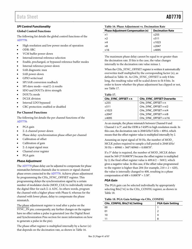
Data Sheet AD7770
Rev. D | Page 41 of 97
SPI Control Functionality
Global Control Functions
The following list details the global control functions of the AD7770:
High resolution and low power modes of operation ODR: SRC VCM buffer power-down Internal/external reference selection Enable, precharged, or bypassed reference buffer modes Internal reference power-down SAR diagnostic mux SAR power-down GPIO write/read SPI SAR conversion readback SPI slave mode—read Σ-Δ results SDO and DOUTx drive strength DOUTx mode DCLK division Internal LDO bypassed CRC protection: enabled or disabled
Per Channel Functions
The following list details the per channel functions of the AD7770:
PGA gain Σ-Δ channel power-down Phase delay: synchronization phase offset per channel Calibration of offset Calibration of gain Σ-Δ input signal mux Channel error register PGA gain
Phase Adjustment
The AD7770 phase delay can be adjusted to compensate for phase mismatches between channels due to sensors or signal channel phase errors connected to the AD7770. Achieve phase adjustment by programming the CHx_SYNC_OFFSET register. This programming delays the synchronization signal by a certain number of modulator clocks (MOD_CLK) to individually initiate the digital filter for each Σ-Δ ADC. In others words, program the channel with a higher phase with Phase 0, whereas for the channel with lower phase, delay to compensate the phase mismatch.
The phase adjustment register is read after a pulse on the SYNC_IN pin; consequently, any further changes on the register have no effect unless a pulse is generated (see the Digital Reset and Synchronization Pins section for more information on how to generate a pulse in the pin).
The phase offset register is multiplied internally by a factor (n) that depends on the decimation rate, as shown in Table 16.
Table 16. Phase Adjustment vs. Decimation Rate Phase Adjustment Compensation (n) Decimation Rate ×1 ≤255 ×2 ≤511 ×4 ≤1023 ×8 ≤2047 ×16 ≤4095
The maximum phase delay cannot be equal to or greater than the decimation rate. If this is the case, the value changes internally to the decimation rate value minus 1.
When the CHx_SYNC_OFFSET register is written it automatically overwrites itself multiplied by the corresponding factor (n), as defined in Table 16. As CHx_SYNC_OFFSET is only 8 bits long, the resulting value will be scaled down to fit 8 bits. In order to know whether the phase adjustment has clipped or not, see Table 17.
Table 17. CHx_SYNC_OFFSET × n CHx_SYNC_OFFSET Overwrite ≤255 CHx_SYNC_OFFSET × n ≤511 CHx_SYNC_OFFSET × n/2 ≤1023 CHx_SYNC_OFFSET × n/4 ≤2047 CHx_SYNC_OFFSET × n/8 ≤4095 CHx_SYNC_OFFSET × n/16
As an example, the phase mismatch between Channel 0 and Channel 1 is 5°, and the ODR is 5 kSPS in high resolution mode. In this case, the decimation rate is 2048 kHz/5 kHz = 409.6, which means that the offset register value is multiplied internally by 2. Assuming an input signal of 50 Hz, the number of MOD_ MCLK pulses required to sample a full period is 2048 kHz/ 50 Hz = 40960 > 360°/40960 = 0.00878°.
If a 5° delay is required, the number of MOD_MCLK delays must be 569 (5°/0.00878°) because the offset register is multiplied by 2; the final offset register value is 409.6/2 − 569/2, which gives a negative value. In this case, if the offset value programmed to the register is higher than 204 (for example, 210 × 2 = 420), the value is internally changed to 408, resulting in a phase compensation of 408 × 0.00878° = 3.58°.
PGA Gain
The PGA gain can be selected individually by appropriately selecting Bits[7:6] in the CHx_CONFIG register, as shown in Table 18.
Table 18. PGA Gain Settings via CHx_CONFIG CHx_CONFIG, Bits[7:6] Setting PGA Gain Setting 00 1 01 2 10 4 11 8

AD7770 Data Sheet
Rev. D | Page 42 of 97
If the Σ-Δ reference is updated, it is recommended to apply a pulse on the SYNC_IN pin to remove invalid samples during the transition of the reference
Decimation
The decimation defines the sampling frequency as follows:
• In high resolution mode, the sampling frequency = MCLK/ (4 × decimation)
• In low power mode, the sampling frequency = MCLK/ (8 × decimation)
Refer to the Sample Rate Converter (SRC section for more information.
GPIOx Pins
If the AD7770 operates in SPI control mode, the mode pins operate as GPIOx pins, as shown in Figure 100. The GPIOx pins can be configured as inputs or outputs in any order.
REGISTERMAP
GPIO0
GPIO1
GPIO2
1253
8-11
7
Figure 100. GPIOx Pin Functionality
Configuration control and readback of the GPIOx pins are set via Bits[2:0] in the GPIO_CONFIG register (0 = input, 1 = output)
and the GPIO_DATA register. Among other uses, the GPIOs can control an external mux connected to the auxiliary inputs of the SAR ADC. Use this mux to verify the results on the Σ-Δ ADCs.
In addition, the GPIOx pins can be used to externally trigger a new decimation rate. Refer to the Sample Rate Converter (SRC section for more information about this functionality.
Σ-Δ Reference Configuration
The AD7770 can operate with internal or external references. In addition, for diagnostic purposes, the analog supply can be used as a reference, as shown in Table 19. REFx−/REFx+ allows the selection of a voltage reference where the REFx+ is lower voltage than REFx− pin.
Table 19. Σ-Δ References Setting for ADC_MUX_CONFIG, Bits[7:6]
Channel 0 to Channel 3
Channel 4 to Channel 7
00 REF1+/REF1− REF2+/REF2− 01 Internal reference Internal reference 10 AVDD1A/AVSS1A AVDD1B/AVSS1B 11 REF1−/REF1+ REF2−/REF2+
Reference buffer operation is described in Table 20. The selected reference and buffer operation mode affect all channels.
If the Σ-Δ reference is updated, it is recommended to apply a pulse on the SYNC_IN pin to remove invalid samples during the transition of the reference.
Table 20. Reference Buffer Operation Modes Reference Buffer Operation Mode REFx+ REFx− Enabled BUFFER_CONFIG_1, Bit 4 = 1; BUFFER_CONFIG_2, Bit 7 = 0 BUFFER_CONFIG_1, Bit 3 = 1; BUFFER_CONFIG_2, Bit 6 = 0 Precharged BUFFER_CONFIG_1, Bit 4 = 1; BUFFER_CONFIG_2, Bit 7 = 1 BUFFER_CONFIG_1, Bit 3 = 1; BUFFER_CONFIG_2, Bit 6 = 1 Disabled BUFFER_CONFIG_1, Bit 4 = 0 BUFFER_CONFIG_1, Bit 3 = 0
Table 21. Additional Disable Power-Down Blocks Block Register Notes VCM GENERAL_USER_CONFIG_1, Bit 5 Enable by default Reference Buffer BUFFER_CONFIG_1, Bits[4:3] Precharged mode by default Internal Reference Buffer GENERAL_USER_CONFIG_1, Bit 4 Disable by default Σ-Δ Channel CH_DISABLE, Bits[7:0] All channels enable SAR GENERAL_USER_CONFIG_1, Bit 3 Disable by default Internal Oscillator GENERAL_USER_CONFIG_1, Bit 2 Enable by default

Data Sheet AD7770
Rev. D | Page 43 of 97
Power Modes
The AD7770 offers different power modes to improve the power efficiency, high resolution and low power mode, which can be controlled via GENERAL_USER_CONFIG_1, Bit 6. To further reduce the power, additional blocks can be disabled independently, as described in Table 21.
If the power mode changes, a pulse on the SYNC_IN pin is required.
LDO Bypassing
The internal LDOs can be individually bypassed and an external supply can be applied directly to the AREG1CAP, AREG2CAP, or DREGCAP pin. Table 22 shows the absolute minimum and maximum supplies for these pins, as well as the associated register used to bypass the regulator.
Table 22. LDO Bypassing
LDO BUFFER_CONFIG_2, Bits[2:0]1
Supply Max (V) Min (V)
AREG1CAP 1XX 1.9 1.85 AREG2CAP X1X 1.9 1.85 DREGCAP XX1 1.98 1.65 1 X means don’t care.
DIGITAL SPI The SPI serial interface on the AD7770 consists of four signals: CS, SDI, SCLK, and SDO. A typical connection diagram of the SPI is shown in Figure 101.
DSP/FPGAAD7770
CS
SCLK
SDI
SDO
1253
8-11
8
Figure 101. SPI Control Interface—AD7770 is the SPI Slave, Digital Signal
Processor (DSP)/Field Programmable Gate Array (FPGA) is the Master
The SPI operates in Mode 0 and Mode 3: CPOL = 0, CPHA = 0 (Mode 0) or CPOL = 1, CPHA = 1 (Mode 3).
In pin control mode, the SDO can read back the Σ-Δ results, depending on the level of the CONVST_SAR pin, as described in Table 13.
In SPI control mode, the SPI transfers data into the on-chip registers while the SDO pin reads back data from the on-chip registers or reads the SAR or the Σ-Δ conversions results, depending on the selected operation mode.
The SDO data source in SPI control mode is defined by the GENERAL_USER_CONFIG_2 and GENERAL_USER_ CONFIG_3 registers, as described in Table 23.
Table 23. SPI Operation Mode in SPI Control Mode GENERAL_USER_ CONFIG_2, Bit 5 Setting
GENERAL_USER_ CONFIG_3, Bit 4 Setting1 Mode
0 0 Internal register 0 1 Σ-Δ data conversion 1 X SAR conversion 1 X means don’t care.
In SPI control mode, there are four different levels of I/O strength on the SDO pin that can be selected in GENERAL_USER_ CONFIG_2, Bits[4:3], as described in Table 24.
Table 24. SDO Strength GENERAL_USER_CONFIG_2, Bits[4:3] Setting Mode 00 Nominal 01 Strong 10 Weak 11 Extra strong
SCLK is the serial clock input for the device. All data transfers (on either SDO or SDI) occur with respect to this SCLK signal.
The SPI can operate in multiples of eight bits. For example, in SPI control mode, if the SDO pin is used to read back the data from the internal register or the SAR ADC, the data frame is 16 bits wide (CRC disabled), as shown in Figure 102, or 24 bits wide (CRC enabled), as shown in Figure 103. In this case, the controller can generate one frame of 16 bits or 24 bits (with and without the CRC enabled), or 2 or 3 frames of 8 bits (with and without the CRC enabled). When the SDO pin reads back the data from the Σ-Δ channels, 64 bits must be read back from the controller (in this case, the controller can generate a frame of 64 bits—either 2 × 32 bits, 4 × 16 bits, or 8 × 8 bits).
SPI CRC—Checksum Protection (SPI Control Mode)
The AD7770 has a checksum mode that improves SPI robustness in SPI control mode. Using the checksum ensures that only valid data is written to a register and allows data read from the device to be validated. The SPI CRC can be enabled by setting the SPI_CRC_TEST_EN bit. If an error occurs during a register write, the SPI_CRC_ERR is set in the error register.
Enabling the SPI_CRC_TEST_EN bit results in a CRC checksum being performed on all the R/W operations. When SPI_ CRC_TEST_EN is enabled, an 8-bit CRC word is appended to every SPI transaction for SAR and register map operations. For more information on Σ-Δ readback operations, see the CRC Header section.
To ensure that the register write is successful, it is recommended to read back the register and verify the checksum.
For CRC checksum calculations, the following polynomial is always used: x8 + x2 + x + 1. See the SPI Control Mode Checksum section for more information.

AD7770 Data Sheet
Rev. D | Page 44 of 97
SPI Read/Write Register Mode (SPI Control Mode)
The AD7770 has on-board registers to configure and control the device.
The registers have 7-bit addresses—the 7-bit register address on the SDI line selects the register for the read/write function. The 7-bit register address follows the R/W bit in the SDI data. The 8 bits on the SDI line following the 7-bit register address are the data to be written to the selected register if the SPI is a write transfer. Data on the SDI line is clocked into the AD7770 on the rising edge of SCLK, as shown in Figure 3.
The data on the SDO line during the SPI transfer contains the 8-bit 0010 0000 header: 8 bits of register data in the case of a read (R) operation, or 8 zeros in the case of a write (W) operation.
With the CRC disabled, the basic data frame on the SDI line during the transfer is 16 bits long, as shown in Figure 102. When the CRC is enabled, a minimum frame length of 24 SCLK periods are required on SPI transfers. The 24 bits of data on the SDO line consist of an 8-bit header (0010 0000), 8 bits of data, and an 8-bit CRC (see Figure 103).
R/W A6 A5 A4 A3 A2 A1 A0 D6D7 D5 D4 D3 D2 D1 D0
0SDO
CS
SCLK
SDI
0 1 0 0 0 0 0 R7 R6 R5 R4 R3 R2 R1 R0
1253
8-11
9
Figure 102. 16-Bit SPI Transfer—CRC Disabled
R/W A6 A5 A4 A3 A2 A1 A0 D6D7 D5 D4 D3 D2 D1 D0 ICRC7 ICRC6 ICRC5 ICRC4 ICRC3 ICRC2 ICRC1 ICRC0
0SDO
CS
SCLK
SDI
0 1 0 0 0 0 0 R7 R6 R5 R4 R3 R2 R1 R0 ICRC7 ICRC6 ICRC5 ICRC4 ICRC3 ICRC2 ICRC1 ICRC0
1253
8-12
0
Figure 103. 24-Bit SPI Transfer—CRC Enabled

Data Sheet AD7770
Rev. D | Page 45 of 97
SPI SAR Diagnostic Mode (SPI Control Mode)
Setting Bit 5 in the GENERAL_USER_CONFIG_2 register configures the SDO line to shift out data from the SAR ADC conversions, as described in Table 23.
In SAR mode, the AD7770 internal registers can be written to, but any readback command is ignored because the SDO data frame is dedicated to shift out the conversion results from the SAR ADC.
To exit this mode of operation, reset Bit 5 in the GENERAL_ USER_CONFIG_2 register.
The data on the SDO line during the SPI transfer contains a 4-bit 0010 header and the 12-bit SAR conversion result if the CRC is disabled.
When the CRC is enabled, a minimum frame length of 24 SCLK periods are required on SPI transfers. The 24 bits of data on the SDO line consist of a 4-bit header (0010), the 12-bit data, and an 8-bit CRC, as shown in Figure 104.
Per the SPI read/write register mode (see the SPI Read/Write Register Mode section), the SDI line contains the R/W bit, a 7-bit register address, the 8-bit data, and an 8-bit CRC (if enabled). To avoid unwanted writes to the internal register while the SAR conversions are read back through the SDO line, it is recom-mended to send a readback command, for example, 0x8000,
to the device, which is ignored because the SDO pin shifts out the content of the SAR ADC.
If consecutive conversions are performed in the SAR ADC, read back the result from the previous conversion before a new conversion is generated. Otherwise, the results are corrupted.
Σ-Δ Data, ADC Mode
In pin control mode, the SPI can be used to read back the Σ-Δ conversions as described in Table 13. In SPI control mode, the SPI reads back the Σ-Δ conversions by setting GENERAL_USER_ CONFIG_3, Bit 4, as described in Table 23; in this mode, the AD7770 internal register can be written to, but any readback command is ignored because the SDO data frame is dedicated to shifting out the conversion results from the Σ-Δ ADCs. To avoid unwanted writes to the internal register, it is recommended to send a readback command, for example, 0x8000, to the device, which is ignored because the SDO pin shifts out the content of the Σ-Δ ADC.
The SDO pin data can be read back in any multiple of 8 bits, for example, as 64 bits, 2 × 32 bits, 4 × 16 bits, or 8 × 8 bits. See the 24-bit example in Figure 105.
SPI Software Reset
Keeping the SDI pin high during 64 consecutives clocks generates a software reset.
R/W A6 A5 A4 A3 A2 A1 A0 D6D7 D5 D4 D3 D2 D1 D0 ICRC7 ICRC6 ICRC5 ICRC4 ICRC3 ICRC2 ICRC1 ICRC0
0SDO
CS
SCLK
SDI
0 1 0 SAR11
SAR10
SAR9
SAR8
SAR6
SAR7
SAR5
SAR4
SAR3
SAR2
SAR1
SAR0 ICRC7 ICRC6 ICRC5 ICRC4 ICRC3 ICRC2 ICRC1 ICRC0
1253
8-12
1
Figure 104. SAR ADC/Diagnostic Mode—CRC Enabled
12
538-
301
DRDY
CS
SCLK
SDI 0x800000
SDO
0x800000
HEADERCH0 D23 TO D8CH0 D7 TO D0CH0 HEADERCH1 D23 TO D16CH1 Figure 105. SPI Used to Read Back the Σ-Δ ADC Data, in 24-Bit Frames

AD7770 Data Sheet
Rev. D | Page 46 of 97
RMS NOISE AND RESOLUTION Table 25 through Table 27 show the dynamic range (DR), rms noise referred to input (RTI), effective number of bits (ENOB), and effective resolution (ER) of the AD7770 for various output data rates and gain settings. The numbers given are for the bipolar input range with an external 2.5 V reference. These numbers are typical and are generated with a differential input voltage of 0 V when the ADC is continuously converting on a single channel.
It is important to note that the effective resolution is calculated using the rms noise; 16,384 consecutives samples were used to calculate the rms noise.
Effective Resolution = log2(Input Range/RMS Noise)
ENOB = (DR − 1.78)/6
HIGH RESOLUTION MODE
Table 25. DR and RTI for High Resolution Mode Decimation Rate
Output Data Rate (SPS) f−3 dB (Hz)
Gain = 1 Gain = 2 Gain = 4 Gain = 8
DR (dB) RTI (μV rms) DR (dB) RTI (μV rms) DR (dB) RTI (μV rms) DR (dB) RTI (μV rms)
64 32,000 8369 103.20 12.10 101.96 6.97 99.20 4.71 95.30 3.82 128 16,000 4818.8 109.43 6.00 108.30 3.39 105.07 2.38 100.71 1.94 256 8000 2511 112.97 4.00 112.38 2.13 110.23 1.39 105.98 1.13 512 4000 1269 116.00 2.80 115.86 1.45 113.68 0.92 109.81 0.7 1024 2000 636.3 119.00 1.98 119.19 1.01 116.75 0.65 113.12 0.51 2048 1000 318.5 123.00 1.38 121.98 0.72 119.79 0.46 115.88 0.35
Table 26. ENOB and ER for High Resolution Mode Decimation Rate
Output Data Rate (SPS) f−3 dB (Hz)
Gain = 1 Gain = 2 Gain = 4 Gain = 8
ENOB (Bits) ER (Bits) ENOB (Bits) ER (Bits) ENOB (Bits) ER (Bits) ENOB (Bits) ER (Bits) 64 32,000 8369 17.14 18.66 16.94 18.45 16.48 18.02 15.83 17.32 128 16,000 4818.8 18.18 19.67 17.99 19.49 17.45 19.00 16.73 18.30 256 8000 2511 18.76 20.25 18.67 20.16 18.31 19.78 17.6 19.08 512 4000 1269 19.27 20.77 19.24 20.72 18.88 20.38 18.24 16.39 1024 2000 636.3 19.77 21.27 19.8 21.24 19.39 20.89 18.79 20.23 2048 1000 318.5 20.43 21.79 20.26 21.73 19.9 21.39 19.25 20.76
LOW POWER MODE
Table 27. DR and RTI for Low Power Mode Decimation Rate
Output Data Rate (SPS) f−3 dB (Hz)
Gain = 1 Gain = 2 Gain = 4 Gain = 8
DR (dB) RTI (μV rms) DR (dB) RTI (μV rms) DR (dB) RTI (μV rms) DR (dB) RTI (μV rms) 64 8000 2092.2 102.8 12.5 101.63 7.19 99.35 4.84 93.96 4.15 128 4000 1204.8 108.94 6.45 108.38 3.51 104.7 2.47 100.25 2.12 256 2000 627.75 112.7 4.23 112.01 2.24 109.4 1.49 105.18 1.18 512 1000 317.25 115.83 2.94 115 1.51 112.95 0.99 109.14 0.77 1024 500 159.25 118.97 2.04 118.72 1.05 116.43 0.67 112.47 0.54
Table 28. ENOB and ER for Low Power Mode Decimation Rate
Output Data Rate (SPS) f−3 dB (Hz)
Gain = 1 Gain = 2 Gain = 4 Gain = 8
ENOB (Bits) ER (Bits) ENOB (Bits) ER (Bits) ENOB (Bits) ER (Bits) ENOB (Bits) ER (Bits) 64 8000 2092.2 17.07 18.61 16.88 18.41 16.5 17.98 15.61 17.2 128 4000 1204.8 18.09 19.56 18.00 19.44 17.39 18.95 16.65 18.17 256 2000 627.75 18.72 20.17 18.60 20.09 18.17 19.68 17.47 19.01 512 1000 317.25 19.24 20.70 19.10 20.66 18.76 20.27 18.13 19.62 1024 500 159.25 19.76 21.22 19.72 21.18 19.34 20.84 18.68 20.15

Data Sheet AD7770
Rev. D | Page 47 of 97
DIAGNOSTICS AND MONITORING SELF DIAGNOSTICS ERROR The AD7770 includes self diagnostic features to guarantee the correct operation. If an error is detected, the ALERT pin is pulled high to generate an external interruption to the controller. In addition, the header of the Σ-Δ output data contains an alert bit that informs the controller of a chip error (see the ADC Conversion Output—Header and Data section).
Both the ALERT pin and bit (status header) are automatically cleared if the error is no longer present. The errors related to the SPI do not recover automatically; read back the appropriate register to clear the error. The ALERT pin and bit reset in the next SPI access after the bit is read back.
If an error detector is manually disabled, it does not generate an internal error and, consequently, the register map or the ALERT pin and bit are not triggered.
There are different sources of errors, as described in Table 29. In pin control code, it is not possible to check the error source, and some sources of error are not enabled. In SPI control mode, check the source of an error by reading the appropriate register bit.
The STATUS_REG_x register bits identify the register that generates an error, as summarized in Table 29.
Table 29. Register Error Source Bit Name Register Source ERR_LOC_GEN2 GEN_ERR_REG_2 ERR_LOC_GEN1 GEN_ERR_REG_1 ERR_LOC_CH7 CH7_ERR_REG ERR_LOC_CH6 CH6_ERR_REG ERR_LOC_CH5 CH5_ERR_REG ERR_LOC_CH4 CH4_ERR_REG ERR_LOC_CH3 CH3_ERR_REG ERR_LOC_CH2 CH2_ERR_REG ERR_LOC_CH1 CH1_ERR_REG ERR_LOC_CH0 CH0_ERR_REG ERR_LOC_SAT_CH6_7 CH6_7_SAT_ERR ERR_LOC_SAT_CH4_5 CH4_5_SAT_ERR ERR_LOC_SAT_CH2_3 CH2_3_SAT_ERR ERR_LOC_SAT_CH0_1 CH0_1_SAT_ERR
In addition, the STATUS_REG_x registers have a bit that indicates if any internal error bit is set, ERROR. This bit clears if the error is no longer present and the register is read back.
The INIT_COMPLETE bit in the STATUS_REG_3 indicates that the device is initialized correctly. This bit is not an error bit but an indicator.
General Errors
MCLK Switch Error (SPI Control Mode)
After power-up, the AD7770 initiates a clocking handover sequence to pass clocking control to the external oscillator, or the CMOS clock. In SPI mode, if an error occurs in the handover,
the EXT_MCLK_SWITCH_ERR bit is set in the general error register, GEN_ERR_REG_2.
If EXT_MCLK_SWITCH_ERR is set, the device is operating off the internal oscillator, and is waiting for an appropriate external clock.
To use a slow external clock (<265 kHz), set the CLK_QUAL_ DIS bit. Setting this bit also clears the error bit.
If the external clock is between 132 kHz and 265 kHz, depending on the internal synchronization between the internal oscillator and the external clock, the error may not trigger. However, it is still recommended to set the CLK_QUAL_DIS bit.
If a slow clock is not in use and the error triggers, a reset is required.
Reset Detection
The AD7770 general error register contains a RESET_DETECTED bit. This bit is asserted if a reset pulse is applied to the AD7770 and is cleared by reading the general error register. This bit indicates that the power-on reset (POR) initialized correctly on the device. In addition, this bit can detect an unexpected device reset or glitch on the RESET pin. To reset this error signal in SPI control mode, toggle the SYNC_IN pin or read from the general error register, GEN_ERR_REG_2. To reset this error signal in pin control mode, toggle the SYNC_IN pin.
Internal LDO Status
The AD7770 has three internal LDOs to regulate the internal analog and digital supply rails. The LDOs have internal power supply monitors. Internal comparators monitor and flag errors with these supplies after they pass a predetermined limit.
The ALDO1_PSM_ERR, ALDO2_PSM_ERR, and DLDO_PSM_ ERR bits indicate either an LDO malfunction, or, if the LDOs are bypassed, an incorrect external supply.
The internal analog and digital voltage monitors can be disabled by appropriately selecting the LDO_PSM_TEST_EN bits.
Use the SAR ADC to verify the error.
Additionally, the levels of the internal monitors can be manually triggered to check if the detector works correctly by appropriately setting the LDO_PSM_TRIP_TEST_EN bits. These bits increase the comparator window threshold above the LDO outputs, forcing the comparator to trigger.
ROM and Memory Map CRC
If an error is found at power-up during the ROM verification, or if the internal memory map is corrupted, the AD7770 generates an error and sets MEMMAP_CRC_ERR or ROM_ CRC_ERR, depending on the source of the error.
The checker can be disabled by clearing the MEMMAP_ CRC_TEST_EN and ROM_CRC_TEST_EN bits. The device must be reset if any of these errors trigger.

AD7770 Data Sheet
Rev. D | Page 48 of 97
Σ-Δ ADC Errors
Reference Detect (SPI Control Mode)
In SPI control mode, the AD7770 includes on-chip circuitry to detect if there is a valid reference for conversions or calibrations. If the voltage between the selected REFx+ and REFx− pins goes below 0.7 V, the AD7770 detects that it no longer has a valid reference. CHx_ERR_REF_DET can be interrogated to identify the affected channel, which clears the bit register if the error is no longer present. The voltage detector can be disabled by clearing the REF_DET_TEST_EN bit.
Use the Σ-Δ ADC diagnostic or the SAR ADC to verify the error.
Overvoltage and Undervoltage Events
The AD7770 includes on-chip overvoltage/undervoltage circuitry on each analog input pin. When the voltage on an analog input pin goes above AVDD1x + 40 mV, the CHx_ ERR_AINx_OV bit is set. The error disappears if the input voltage falls below AVDD1x − 40 mV.
If an undervoltage event occurs (AVSSx − 40 mV), the CHx_ ERR_AINx_UV bit is set. The error disappears if the input voltage increases to AVSSx + 40 mV.
The CHx_ERR_AINM_UV, CHx_ERR_AINM_OV, CHx_ERR_ AINP_UV, and CHx_ERR_AINP_OV bits can be read back to verify the affected channel input, which clears the bits if the error is no longer present. The overvoltage and undervoltage detection can be disabled independently by clearing the AINM_ UV_TEST_EN, AINM_OV_TEST_EN, AINP_UV_TEST_EN, or AINP_OV_TEST_EN bits.
The input voltage can be checked independently with the SAR ADC.
Modulator Saturation
The AD7770 includes modulator saturation detection on each of the Σ-Δ ADCs. If 20 consecutive codes for the modulator are either all 1s or 0s, this condition is flagged as a modulator saturation event. Reading the CHx_ERR_MOD_SAT register clears the bit if the error corrects itself.
Modulator saturation detection can be disabled by clearing the MOD_SAT_TEST_EN bit.
Note that the modulator input voltage is attenuated internally, which means that a modulator output of all 1s or 0s represents a modulator that is out of bounds and that a RESET pulse is required.
Filter Saturation
TheAD7770 includes digital filter saturation detection on each Σ-Δ ADC channel. This detection indicates that the filter output is out of bounds, which represents an output code approximately 20% higher than positive or negative full scale. Reading the CHx_ERR_ FILTER_SAT bit clears the bit if the error corrects itself.
The detection can be disabled by clearing FILTER_SAT_TEST_ EN bit.
Output Saturation
An output saturation event can occur when gain and offset calibration causes the output from the digital filter to clip at either positive or negative full scale. The output does not wrap. Reading the CHx_ERR_OUTPUT_SAT bit clears the bit if the error corrects itself.
The detection can be disabled by clearing OUTPUT_SAT_ TEST_EN bit.
SPI Transmission Errors (SPI Control Mode)
All SPI errors clear after reading GEN_ERR_REG_1, which contains the SPI errors. These errors are not recovered auto-matically and, consequently, the ALERT pin and bit remain set until the error register is read back, and a new SPI frame is generated.
CRC Checksum Error
If the CRC checksum is enabled by setting the SPI_CRC_ TEST_EN bit, an error bit, SPI_CRC_ERR, is raised if the CRC message does not match the message computed by the AD7770 internal CRC block. If the CRC message does not match the internally computed message, the register is not updated.
SCLK Counter
If the number of clocks generated by the controller is not a multiple of 8 after CS is pulled high, an error bit, SPI_CLK_ COUNT_ERR is raised. The last command multiple of 8 is executed; however, the SCLK counter can be disabled by setting the SPI_CLK_COUNT_TEST_EN bit.
Invalid Read
When attempting to read back an invalid register address, the SPI_INVALID_READ_ERR bit is set.
The invalid readback address detection can be disabled by setting the SPI_INVALID_READ_TEST_EN bit.
Invalid Write
When attempting to write to an invalid register address or a read only register, the SPI_INVALID_WRITE_ERR bit is set.
The invalid write address detection can be disabled by setting the SPI_INVALID_WRITE_TEST_EN bit.
MONITORING USING THE AD7770 SAR ADC (SPI CONTROL MODE) The AD7770 contains an on-chip SAR ADC for chip diagnostics, system diagnostics, or measurement verification. The SAR ADC has a 12-bit resolution. The AVDD4 and AVSS4 pins operate in complete independence of the Σ-Δ ADC supplies and, therefore, can be used for chip diagnostics in systems where functional safety is important. The reference for the SAR conversion process is taken from the SAR ADC supply voltage (AVDD4/ AVSS4) and, therefore, the SAR analog input range is from AVSS4 to AVDD4.
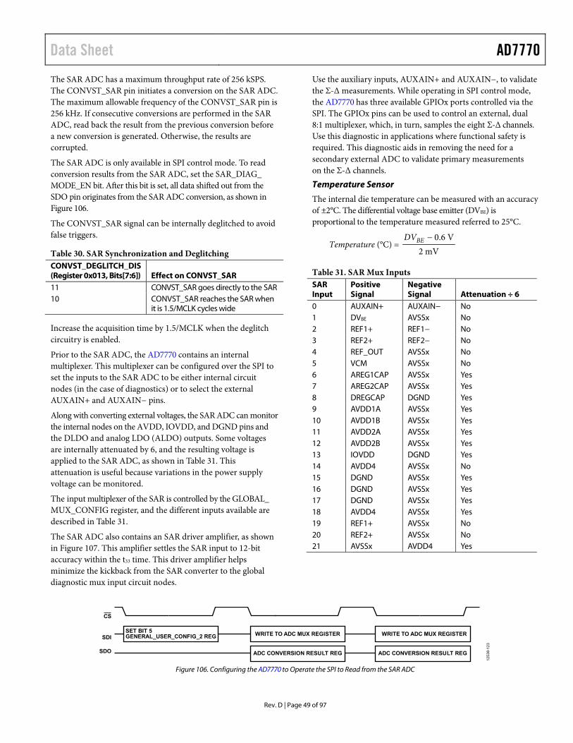
Data Sheet AD7770
Rev. D | Page 49 of 97
The SAR ADC has a maximum throughput rate of 256 kSPS. The CONVST_SAR pin initiates a conversion on the SAR ADC. The maximum allowable frequency of the CONVST_SAR pin is 256 kHz. If consecutive conversions are performed in the SAR ADC, read back the result from the previous conversion before a new conversion is generated. Otherwise, the results are corrupted.
The SAR ADC is only available in SPI control mode. To read conversion results from the SAR ADC, set the SAR_DIAG_ MODE_EN bit. After this bit is set, all data shifted out from the SDO pin originates from the SAR ADC conversion, as shown in Figure 106.
The CONVST_SAR signal can be internally deglitched to avoid false triggers.
Table 30. SAR Synchronization and Deglitching CONVST_DEGLITCH_DIS (Register 0x013, Bits[7:6]) Effect on CONVST_SAR 11 CONVST_SAR goes directly to the SAR 10 CONVST_SAR reaches the SAR when
it is 1.5/MCLK cycles wide
Increase the acquisition time by 1.5/MCLK when the deglitch circuitry is enabled.
Prior to the SAR ADC, the AD7770 contains an internal multiplexer. This multiplexer can be configured over the SPI to set the inputs to the SAR ADC to be either internal circuit nodes (in the case of diagnostics) or to select the external AUXAIN+ and AUXAIN− pins.
Along with converting external voltages, the SAR ADC can monitor the internal nodes on the AVDD, IOVDD, and DGND pins and the DLDO and analog LDO (ALDO) outputs. Some voltages are internally attenuated by 6, and the resulting voltage is applied to the SAR ADC, as shown in Table 31. This attenuation is useful because variations in the power supply voltage can be monitored.
The input multiplexer of the SAR is controlled by the GLOBAL_ MUX_CONFIG register, and the different inputs available are described in Table 31.
The SAR ADC also contains an SAR driver amplifier, as shown in Figure 107. This amplifier settles the SAR input to 12-bit accuracy within the t33 time. This driver amplifier helps minimize the kickback from the SAR converter to the global diagnostic mux input circuit nodes.
Use the auxiliary inputs, AUXAIN+ and AUXAIN−, to validate the Σ-Δ measurements. While operating in SPI control mode, the AD7770 has three available GPIOx ports controlled via the SPI. The GPIOx pins can be used to control an external, dual 8:1 multiplexer, which, in turn, samples the eight Σ-Δ channels. Use this diagnostic in applications where functional safety is required. This diagnostic aids in removing the need for a secondary external ADC to validate primary measurements on the Σ-Δ channels.
Temperature Sensor
The internal die temperature can be measured with an accuracy of ±2°C. The differential voltage base emitter (DVBE) is proportional to the temperature measured referred to 25°C.
Temperature (°C) = mV2
V6.0−BEDV
Table 31. SAR Mux Inputs SAR Input
Positive Signal
Negative Signal Attenuation ÷ 6
0 AUXAIN+ AUXAIN− No 1 DVBE AVSSx No 2 REF1+ REF1− No 3 REF2+ REF2− No 4 REF_OUT AVSSx No 5 VCM AVSSx No 6 AREG1CAP AVSSx Yes 7 AREG2CAP AVSSx Yes 8 DREGCAP DGND Yes 9 AVDD1A AVSSx Yes 10 AVDD1B AVSSx Yes 11 AVDD2A AVSSx Yes 12 AVDD2B AVSSx Yes 13 IOVDD DGND Yes 14 AVDD4 AVSSx No 15 DGND AVSSx Yes 16 DGND AVSSx Yes 17 DGND AVSSx Yes 18 AVDD4 AVSSx Yes 19 REF1+ AVSSx No 20 REF2+ AVSSx No 21 AVSSx AVDD4 Yes
CS
SDI
SDO
SET BIT 5GENERAL_USER_CONFIG_2 REG WRITE TO ADC MUX REGISTER WRITE TO ADC MUX REGISTER
ADC CONVERSION RESULT REG ADC CONVERSION RESULT REG
1253
8-12
3
Figure 106. Configuring the AD7770 to Operate the SPI to Read from the SAR ADC

AD7770 Data Sheet
Rev. D | Page 50 of 97
SAR DRIVER
CONTROL LOGIC
FIFO
ON-CHIPDIAGNOSTICS
SPI
AUXAIN+
AUXAIN–
AVDD4
AVSS4
CONVST_SAR
MUX
DEGLITCH
SAR ADC
REF
1253
8-12
2
Figure 107. SAR ADC Configuration and Control
Table 32. Σ-Δ Diagnostic Input Voltage Recommended Voltage Reference Notes/Result 0 Floating Not applicable Not applicable 1 Floating Not applicable Not applicable 2 280 mV differential signal Internal/external PGA gain calibration 3 External reference, positive/negative External Positive full scale 4 External reference, negative/positive External Negative full scale 5 External reference, negative/negative External Zero scale 6 Internal reference, positive/negative Internal Positive full scale 7 Internal reference, negative/positive Internal Negative full scale 8 Internal reference, positive/positive Internal Zero scale 9 External reference, positive/positive External Zero scale
Σ-Δ ADC DIAGNOSTICS (SPI CONTROL MODE) The AD7770 Σ-Δ ADC diagnostic functions are accessible through the SPI. The internal mux placed before the PGA has different inputs, allowing the user to select a zero-scale, positive full-scale, or negative full-scale input to the Σ-Δ ADC, which can be converted to verify the correct operation of the Σ-Δ ADC channel.
The diagnostic mux control signals are shared across all the Σ-Δ channels. Depending on the diagnostic selected, connect the Σ-Δ ADC reference to a different reference source to guarantee that the conversion is within the measurable range.
There are two different ways to enable the diagnostic mux, as follows:
• Setting the CHx_RX bit. This bit enables the input Σ-Δ mux. The multiplexer inputs are described in Table 32. The reference used during the conversions are controlled by the REF_MUX_CTRL bits.
• Setting CHx_REF_MONITOR. This bit has the same effect as enabling the CHx_RX bit and selects the VDD1x/AVSSx supplies as the main reference.
If the AINx± pin is connected to AVSSx, the input range is outside the range of AVSSx + 100 mV; therefore, results may differ slightly from the expected value.
Alternatively, the inputs can be used to calibrate gain and offset errors.

Data Sheet AD7770
Rev. D | Page 51 of 97
Σ-∆ OUTPUT DATA ADC CONVERSION OUTPUT—HEADER AND DATA The AD7770 Σ-Δ conversion results are output on the DOUT0 to DOUT3 pins or over the SPI, depending on the selected interface. If the DOUTx interface is selected, the AD7770 acts as the master in the transmission. If the SPI is selected, the controller is the master.
The DRDY signal indicates the end of conversion independent of the interface selected to read back the Σ-Δ conversion. When the SPI reads back the Σ-Δ conversion, if a new conversion is completed (DRDY falling edge) before the previous conversion is read back, the results from previous conversion are overwritten and, consequently, the previous conversion data is corrupted.
For each channel, the width is 32 bits long: 8 bits for the header and 24 bits for the Σ-Δ conversion, as shown in Figure 108.
ADC DATA NN – 1
24-BITS8-BITS
DOUTx
DRDY
HEADER N
1253
8-12
4
Figure 108. ADC Output—8-Bit Header Plus 24-Bit Conversion Data
In pin control mode, the header is fixed to the CRC while in SPI mode, and can be selected between CRC and error headers.
CRC Header
The CRC header is the header generated in pin control mode or in SPI mode if DOUT_HEADER_FORMAT is set.
As shown in Figure 109, the header consists of an alert bit, three bits for the ADC channel ID, as shown in Table 33, and four bits for the CRC.
The chip error bit is set high if an error is detected in any channel, as explained in the General Errors section. The alert bit remains 1 until the error disappears.
ALERT CH_ID_2 CH_ID_1 CH_ID_0 CRC CRC CRC CRC
1253
8-20
0
Figure 109. CRC Header
Table 33. Channel ID Channel CH_ID_2 CH_ID_1 CH_ID_0 0 0 0 0 1 0 0 1 2 0 1 0 3 0 1 1 4 1 0 0 5 1 0 1 6 1 1 0 7 1 1 1
The CRC generated is eight bits long; the 4 MSBs are placed on the header for the first channel in the pairing and the 4 LSBs on the header of the second channel in the pairing, as shown in Table 34. If a channel is disabled, the 24-bit output data for this channel is 0x000000.
Table 34. 8-Bit CRC, Header Configuration (Channel 2) ALERT 0 1 0 CRC7 CRC6 CRC5 CRC4
Table 35. 8-Bit CRC, Header Configuration (Channel 3) ALERT 0 1 1 CRC3 CRC2 CRC1 CRC0
ERROR Header (SPI Control Mode)
In SPI control mode, the default header can be replaced by an error header. If the Σ-Δ conversion is read back through the SPI, disable the CRC by clearing the SPI_CRC_TEST_EN bit. If the DOUTx interface is used, clear the DOUT_HEADER_ FORMAT bit.
The error header provides information of common error sources specific for each channel, as shown in Table 36. Modulator and filter errors are indicated even if the checker for these errors are specifically disabled, as described in the Σ-Δ ADC Errors section.
Table 36. Status Header Output Bits Name Description 7 Alert This bit is set high if any of the enabled diagnostic functions have detected an error, including an
external clock not detected, a memory map bit flip, or an internal CRC error. This bit is not channel specific. The bit clears if the error is no longer present.
[6:4] CH_ID_[2:0] These bits indicate which ADC channel the following conversion data came from (see Table 33). 3 RESET_DETECTED This bit indicates if a reset condition occurs. This bit is not channel specific. 2 MODULATOR_SATURATE This bit indicates that the modulator output is 20 consecutive 0s or 1s. The bit resets automatically
after the error is no longer present. 1 FILTER_SATURATE This bit indicates that the filter output is out of bounds. The bit resets automatically after the error is
no longer present. 0 AIN_OV_UVERROR This bit indicates that there is an AINx± overvoltage/undervoltage condition on the inputs. This bit is
set until the appropriate register is read back and the error is no longer present.

AD7770 Data Sheet
Rev. D | Page 52 of 97
SAMPLE RATE CONVERTER (SRC) (SPI CONTROL MODE) The AD7770 implements a feature called the SRC on each Σ-Δ channel that allows the user to configure the output data rate or sampling frequency to any desired value, including noninteger values. The SRC achieves fine resolution control over the Σ-Δ ADC ODR. In applications where the ODR must change based on changes in the input signal to maintain sampling coherency, the SRC provides fine control over the ODR. For example, to achieve the highest classification standard, Class A, in power quality applications, coherency must be maintained for 0.01 Hz changes in the input power line. Use the SRC to achieve this sampling frequency accuracy.
In pin control mode, the decimation rate is fixed per the predefined pin control options. Consequently, a noninteger number cannot be selected, as shown in Table 13.
To set the ODR, the user must program up to four registers, depending on the decimation value: two registers to program the integer value, N (the effective decimation rate), and two registers to program the decimal value, the interpolation factor (IF).
The integer value registers are SRC_N_MSB, Bits[3:0] and SRC_N_LSB, Bits[7:0]. The decimal part value registers are SRC_IF_MSB, Bits[7:0] and SRC_IF_LSB, Bits[7:0].
As an example, if an output data rate of 2.8 kHz is required, the decimation rate equates to
• High resolution mode = 2048/2.8 = 731.428 • Low power mode = 512/2.8 = 182.857
The register values for high resolution mode are as follows:
• 731 (decimal) = 0x2DB • SRC_N_MSB, Bits[3:0] = 0x02 • SRC_N_LSB, Bits[7:0] = 0xDB • 0.428 (decimal) = 0.428 × 216 = 28049 (decimal) = 0x6D91 • SRC_IF_MSB, Bits[7:0] = 0x6D • SRC_IF_LSB, Bits[7:0] = 0x91
The SRC resolution depends on the decimal number used in the decimation, as well as the modulator clock (MOD_CLK), as follows:
16216
21232 ×+×+×
=DECDEC
MODResolution MCLK
where: MODMCLK is the modulator frequency. DEC is the decimal portion of the decimation rate.
In high resolution mode, for a decimal decimation of 450, the resolution is defined as
SPS104.15
2145034502
2048 6–
162216
×=××+×
The ODR can be updated on-the-fly, but a new ODR is effective in three conversion cycles of the Σ-Δ ADCs. This condition guarantees a smooth transition with no conversion results out of range.
There are two different ways to change the ODR after a new value is written in the SRC registers: via software or via hardware, depending on SRC_LOAD_SOURCE (SRC_UPDATE register, Bit 7).
If the SRC_LOAD_SOURCE bit is clear, the new ODR value is updated by setting the SRC_LOAD_UPDATE bit to 1. This bit must be held high for at least two MLCK periods; return the bit to 0 before attempting another update.
If SRC_LOAD_SOURCE is set, the GPIO0 pin controls the ODR update externally. Apply a pulse in the GPIO2 pin, which is then internally synchronized with the external MCLK clock, and the resultant synchronous signal is output on the GPIO1 pin.
The GPIO1 and GPIO0 pins must be externally connected.
If multiple AD7770 devices must be synchronized, the GPIO1 pin of one device can be connected to multiple devices. This synchro-nization method requires the use of a common MCLK signal for all the AD7770 devices connected, as shown in Figure 110.
GPIO2
GPIO0
GPIO0
GPIO0
MCLK GPIO1
GPIO2MCLK GPIO1
NC
GPIO2MCLK GPIO1
NC
AD7770
AD7770
AD7770
SYNCHRONIZATIONLOGIC
PULSE
DIGITAL FILTER
SYNCHRONIZATIONLOGIC
DIGITAL FILTER
SYNCHRONIZATIONLOGIC
DIGITAL FILTER
MCLK
1253
8-12
5
NOTES1. NC = NO CONNECT.
Figure 110. Hardware ODR Update

Data Sheet AD7770
Rev. D | Page 53 of 97
SRC Bandwidth
The sinc3 filter architecture allows the user to select a noninteger value as the decimation range This versatility means that the filter notches must be adjusted dynamically: two notches at the variable frequency, and one fixed notch to remove the PGA chopping tone. Consequently, the traditional formula for −0.1 dB and −3 dB bandwidth must be adjusted depending on the selected decimation rate.
The bandwidth transfer function is not linear but can be approximated by using a linear function.
Figure 111 and Figure 112 show the correction factor for the −0.1 dB and −3 dB bandwidth, respectively, in high resolution. In low power mode, the offset must be divided by 4. For example, when the ODR = 1000 SPS in low power mode, the −0.1 dB point is
Hz71436.4710000481.0 BW
0
200
400
600
800
1000
1200
1400
1600
–0.1
dB
FR
EQ
UE
NC
Y (
Hz)
ODR (kHz) 125
38-
12
6
0.1 5.1 10.1 15.1 20.1 25.1 30.1
y = 0.0481x + 47.36
Figure 111. −0.1 dB Correction Factor
9
–3d
B F
RE
QU
EN
CY
(kH
z)
1
2
3
4
5
6
7
8
ODR (kHz)
0
125
38
-12
7
0.1 5.1 10.1 15.1 20.1 25.1 30.1
y = 0.2608x + 248.64
Figure 112. −3 dB Correction Factor
SRC Group Delay and Latency
The SRC group delay depends on the selected ODR and the power mode, and is defined by the following equation:
Group delay = 8 _
_SRC N
SRC N ODR
where: SRC_N is the integer value of the programmed ODR. ODR is the programmed output data rate.
The latency is the contribution of the group delay and the calibration time.
Latency = Group delay + tCAL
where tCAL = 62 × tMCLK, with a maximum error of 2 × tMCLK, in high resolution mode; or 121 × tMCLK, with a maximum error of 4 × tMCLK, in low power mode.
tMCLK is the modulator period, MCLK/4 in high resolution mode and MCLK/8 in low power mode.
Settling Time
The settling time is defined by the contribution of all the internal stages, the filter delay, and the block calibration.
The filter delay is defined as 3/ODR. In some extreme cases, as when an external pulse is applied, this value may increase to 4/ODR.
DATA OUTPUT INTERFACE The Σ-Δ output data interface is defined by the CONVST_SAR, FORMAT0, and FORMAT1 pins in pin control mode at power-up. The FORMATx pins cannot be changed dynamically. Table 14 shows the available options for pin control mode. If the device is configured in SPI control mode, the SPI_SLAVE_MODE_ EN bit enables the SPI to transmit the Σ-Δ ADC conversion results, as shown in Table 23.
DOUT3 to DOUT0 Data Interface
Standalone Mode
In standalone mode, the AD7770 interface acts as a master. There are three different DOUTx configurations, configurable through the FORMATx pins in pin control mode, as shown in Figure 113 through Figure 115, or via the DOUT_FORMAT bits, Bits[7:6], in SPI control mode, as described in Table 37.
Figure 116, Figure 117, and Figure 118 show the expected data outputs for different DOUTx output modes.

AD7770 Data Sheet
Rev. D | Page 54 of 97
Table 37. DOUTx Channels DOUT_FORMAT Bits/FORMATx Pins Number of DOUTx Lines Enabled Associated Channels 00 4 DOUT0—Channel 0 and Channel 1 DOUT1—Channel 2 and Channel 3 DOUT2—Channel 4 and Channel 5 DOUT3—Channel 6 and Channel 7
01 2 DOUT0—Channel 0, Channel 1, Channel 2, and Channel 3 DOUT1—Channel 4, Channel 5, Channel 6, and Channel 7
10 or 11 1 DOUT0—Channel 0, Channel 1, Channel 2, Channel 3, Channel 4, Channel 5, Channel 6, and Channel 7
DOUT0
DOUT1
DOUT2
DOUT3
DCLK
DRDY
FORMAT1
DAISY-CHAINING IS NOT POSSIBLE IN THIS FORMAT
FORMAT0
AD7770
DGND
DOUT0: CH 0, CH 1DOUT1: CH 2, CH 3DOUT2: CH 4, CH 5DOUT3: CH 6, CH 7
00
00
1253
8-12
8
Figure 113. FORMATx Pin Configuration—FORMAT0 = 0, FORMAT1 = 0
DOUT0
DOUT1
DCLK
DRDY
FORMAT1
IOVDD
DAISY-CHAINING IS POSSIBLE IN THIS FORMAT
DGND
FORMAT0CH 0, CH 1, CH 2, CH 3
OUTPUT ON DOUT0
CH 4, CH 5, CH 6, CH 7OUTPUT ON DOUT1
01
10
AD7770
1253
8-12
9
Figure 114. FORMATx Pin Configuration—FORMAT0 = 1, FORMAT1 = 0
DOUT0
DCLK
DRDY
FORMAT1
IOVDD
DAISY-CHAINING IS POSSIBLE IN THIS FORMAT
DGND
FORMAT0CH 0 TO CH 7OUTPUT ON DOUT0
1001
AD7770
1253
8-13
0
Figure 115. FORMATx Pin Configuration—FORMAT0 = 0, FORMAT1 = 1

Data Sheet AD7770
Rev. D | Page 55 of 97
CH0-S0 CH1-S0
CH2-S0 CH3-S0
CH0-S1 CH1-S1
CH2-S1 CH3-S1
DCLK
DRDY
DOUT0
SAMPLE N SAMPLE N + 1
DOUT1
CH4-S0 CH5-S0
CH6-S0 CH7-S0
CH4-S1 CH5-S1
CH6-S1 CH7-S1
DOUT0
DOUT1
1253
8-13
1
Figure 116. FORMAT0 = 0, FORMAT1 = 0—Each DOUTx Outputs Two ADC Conversions (S0 Means Sample 0 and S1 Means Sample 1)
CH0-S0 CH1-S0 CH2-S0 CH3-S0
CH7-S0CH4-S0 CH5-S0 CH6-S0
CH0-S1 CH1-S1 CH2-S1 CH3-S1
CH7-S1CH4-S1 CH5-S1 CH6-S1
DCLK
DRDY
DOUT0
SAMPLE N SAMPLE N + 1
DOUT1
DOUT3
DOUT2
1253
8-13
2
Figure 117. FORMAT0 = 0, FORMAT1 = 1—Channel 0 to Channel 3 Share DOUT0, and Channel 4 to Channel 7 Share DOUT1 (S0 Means Sample 0 and S1 Means Sample 1)
DCLK
DRDY
DOUT0
SAMPLE N SAMPLE N + 1 SAMPLE N + 2
DOUT3
DOUT2
DOUT1
CH0-S0 CH1-S0 CH2-S0 CH...-S0 CH6-S0 CH7-S0 CH0-S1 CH0-S2 CH0-S3CH1-S1 CH2-S1 CH...-S1 CH6-S1 CH7-S2 CH1-S2 CH2-S2 CH...-S2 CH6-S2 CH7-S2
1253
8-13
3
Figure 118. FORMAT0 = 1, FORMAT1 = 0—Channel 0 to Channel 7 Output on DOUT0 Only (S0 Means Sample 0 and S1 Means Sample 1)

AD7770 Data Sheet
Rev. D | Page 56 of 97
Daisy-Chain Mode
Daisy-chaining devices allows numerous devices to use the same data interface lines by cascading the outputs of multiple ADCs from separate AD7770 devices. In daisy-chain configura-tion, only one device has a direct connection between the DOUTx interface and the digital host. For the AD7770, daisy-chain capability is implemented by cascading DOUT0 and DOUT1 through a number of devices, or by just using DOUT0 (the number of DOUTx pins available depends on the selected DOUTx mode). The ability to daisy-chain devices and the limit on the number of devices that can be handled by the chain is dependent on the selected DOUTx mode and the decimation rate employed.
When operating in daisy-chain mode, it is required that all AD7770 devices in the chain are correctly synchronized. See the Digital Reset and Synchronization Pins section for more information.
This feature is especially useful for reducing the component count and wiring connections in, for example, isolated multiconverter applications or for systems with a limited interfacing capacity.
For daisy-chain operation, there are two different configurations possible, as described in Table 38.
Using the FORMATx = 10 mode, DOUT2 acts as an input pin, as shown in Figure 119. In this case, the DOUT0 pin of the AD7770 devices is cascaded to the DOUT2 pin of the next device in the chain. Data readback is analogous to clocking a shift register where data is clocked on the rising edge of DCLK.
Table 38. DOUTx Modes in Daisy-Chain Operation DOUT_FORMAT Bits/ FORMATx Pins Number of DOUTx Lines Enabled Associated Channels 01 2 DOUT0—Channel 0 to Channel 3 and DOUT2 DOUT1—Channel 4 to Channel 7 and DOUT3 DOUT2—input channel DOUT3—input channel 10 1 DOUT0—Channel 0 to Channel 7 and DOUT2 DOUT2—input channel
U2 S0 CH0 TO CH7
U2 S0 CH0 TO CH7
U1 S0 CH0 TO CH7
0
0
U2 S0 CH0 TO CH7
U1 S0 CH0 TO CH7
0
U2 S1 CH0 TO CH7
U2 S1 CH0 TO CH7
U1 S1 CH0 TO CH7
0
0
U2 S1 CH0 TO CH7
U2 S3 CH0 TO CH7
0
U2 S0 CH0 TO CH7
U2 S0 CH0 TO CH7
U1 S1 CH0 TO CH7
0
U2 DOUT0
U1 DOUT2/DIN0
U1 DOUT0
U2 DOUT2/DIN0
DRDY
DCLK
U2
DOUT2/DIN0 DOUT0
U2
DOUT2/DIN0 DOUT0
1253
8-13
4
Figure 119. Daisy-Chain Connection Mode, FORMAT0 = 1, FORMAT1 = 0 (S0 Means Sample 0 and S1 Means Sample 1); When Connected in Daisy-Chain Mode,
DOUT2 Acts as an Input Pin, Represented by DIN0
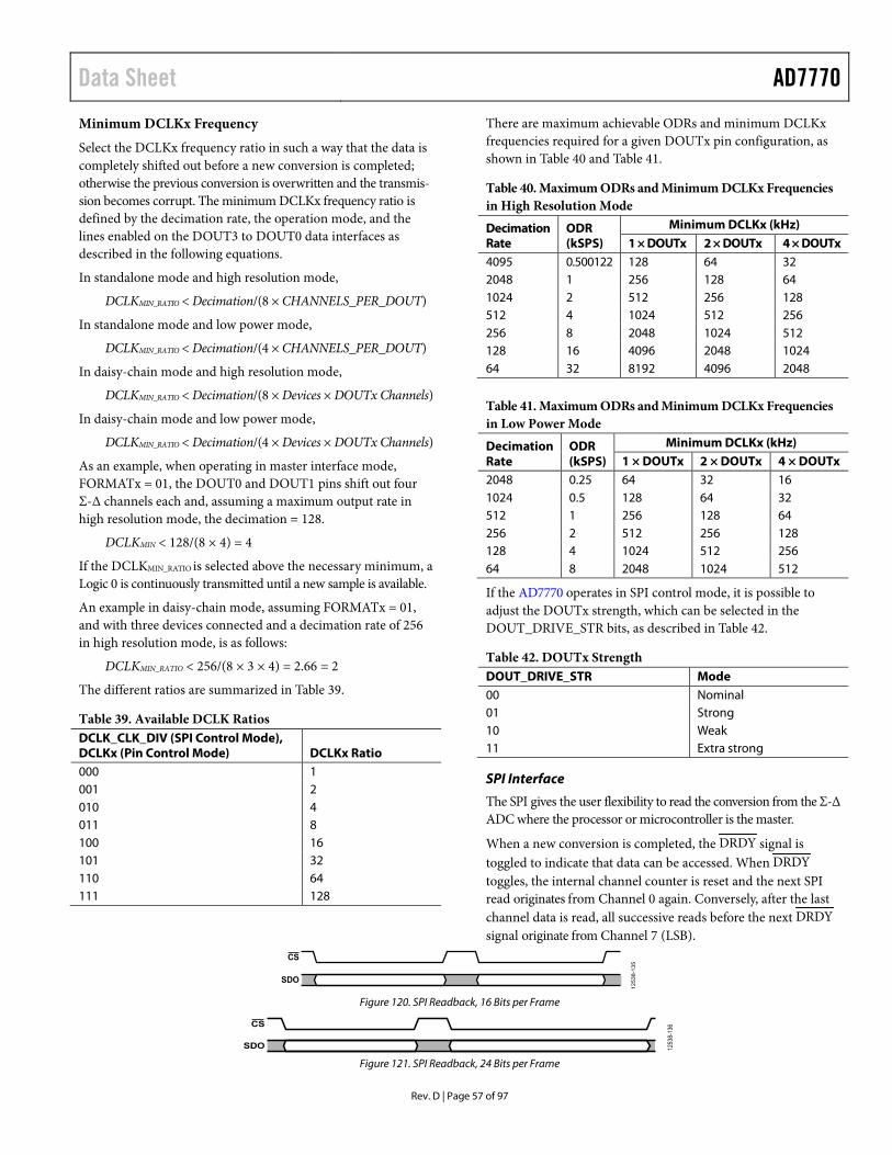
Data Sheet AD7770
Rev. D | Page 57 of 97
Minimum DCLKx Frequency
Select the DCLKx frequency ratio in such a way that the data is completely shifted out before a new conversion is completed; otherwise the previous conversion is overwritten and the transmis-sion becomes corrupt. The minimum DCLKx frequency ratio is defined by the decimation rate, the operation mode, and the lines enabled on the DOUT3 to DOUT0 data interfaces as described in the following equations.
In standalone mode and high resolution mode,
DCLKMIN_RATIO < Decimation/(8 × CHANNELS_PER_DOUT)
In standalone mode and low power mode,
DCLKMIN_RATIO < Decimation/(4 × CHANNELS_PER_DOUT)
In daisy-chain mode and high resolution mode,
DCLKMIN_RATIO < Decimation/(8 × Devices × DOUTx Channels)
In daisy-chain mode and low power mode,
DCLKMIN_RATIO < Decimation/(4 × Devices × DOUTx Channels)
As an example, when operating in master interface mode, FORMATx = 01, the DOUT0 and DOUT1 pins shift out four Σ-Δ channels each and, assuming a maximum output rate in high resolution mode, the decimation = 128.
DCLKMIN < 128/(8 × 4) = 4
If the DCLKMIN_RATIO is selected above the necessary minimum, a Logic 0 is continuously transmitted until a new sample is available.
An example in daisy-chain mode, assuming FORMATx = 01, and with three devices connected and a decimation rate of 256 in high resolution mode, is as follows:
DCLKMIN_RATIO < 256/(8 × 3 × 4) = 2.66 = 2
The different ratios are summarized in Table 39.
Table 39. Available DCLK Ratios DCLK_CLK_DIV (SPI Control Mode), DCLKx (Pin Control Mode) DCLKx Ratio 000 1 001 2 010 4 011 8 100 16 101 32 110 64 111 128
There are maximum achievable ODRs and minimum DCLKx frequencies required for a given DOUTx pin configuration, as shown in Table 40 and Table 41.
Table 40. Maximum ODRs and Minimum DCLKx Frequencies in High Resolution Mode
Decimation Rate
ODR (kSPS)
Minimum DCLKx (kHz) 1 × DOUTx 2 × DOUTx 4 × DOUTx
4095 0.500122 128 64 32 2048 1 256 128 64 1024 2 512 256 128 512 4 1024 512 256 256 8 2048 1024 512 128 16 4096 2048 1024 64 32 8192 4096 2048
Table 41. Maximum ODRs and Minimum DCLKx Frequencies in Low Power Mode
Decimation Rate
ODR (kSPS)
Minimum DCLKx (kHz) 1 × DOUTx 2 × DOUTx 4 × DOUTx
2048 0.25 64 32 16 1024 0.5 128 64 32 512 1 256 128 64 256 2 512 256 128 128 4 1024 512 256 64 8 2048 1024 512
If the AD7770 operates in SPI control mode, it is possible to adjust the DOUTx strength, which can be selected in the DOUT_DRIVE_STR bits, as described in Table 42.
Table 42. DOUTx Strength DOUT_DRIVE_STR Mode 00 Nominal 01 Strong 10 Weak 11 Extra strong
SPI Interface
The SPI gives the user flexibility to read the conversion from the Σ-Δ ADC where the processor or microcontroller is the master.
When a new conversion is completed, the DRDY signal is toggled to indicate that data can be accessed. When DRDY toggles, the internal channel counter is reset and the next SPI read originates from Channel 0 again. Conversely, after the last channel data is read, all successive reads before the next DRDY signal originate from Channel 7 (LSB).
CS
SDO
1253
8-13
5
Figure 120. SPI Readback, 16 Bits per Frame
CS
SDO 1253
8-13
6
Figure 121. SPI Readback, 24 Bits per Frame

AD7770 Data Sheet
Rev. D | Page 58 of 97
The SPI operates in multiples of 8 bits per frame; Figure 120 shows a readback example in 16 bits per frames, and Figure 121 shows a readback in 24 bits per frame.
Note that if the device is configured in SPI control mode, the AD7770 generates a software reset if the SDI pin is sampled high for 64 consecutive clocks. To avoid a reset or unwanted register writes, it is recommended to transfer a 0x8000 command, which generates a readback command that is ignored by the device, as explained in the Σ-Δ Data, ADC Mode section.
CALCULATING THE CRC CHECKSUM The AD7770 implements two different CRC checksum generators, one for the Σ-Δ results and another for the SPI control mode.
The AD7770 uses a CRC polynomial to calculate the CRC checksum value. The 8-bit CRC polynomial used is x8 + x2 + x + 1.
To replicate the polynomial division in hardware, remember that the data is left shifted by eight bits to create a number ending in eight Logic 0s. The polynomial is aligned so that its MSB is adjacent to the leftmost Logic 1 of the data. An exclusive OR (XOR) function is applied to the data to produce a new, shorter number. The polynomial is again aligned so that its MSB is adjacent to the leftmost Logic 1 of the new result, and the procedure is repeated. This process is repeated until the original data is reduced to a value less than the polynomial, the 8-bit checksum.
Note that the AD7770 CRC block preset the input shift registers to 1, meaning that the 8 MSBs of user data must be inverted before compute the algorithm.
An example of the CRC calculation for 12-bit data is shown in Table 43.
Table 43. Example CRC Calculation for 12-Bit Data1 Data 0 0 0 0 0 1 1 0 0 1 0 0 1 1 1 0 0 0 0 0 0 0 0 0 Process Data 1 1 1 1 1 0 0 1 0 1 0 0 1 1 1 0 0 0 0 0 0 0 0 0 Polynomial 1 0 0 0 0 0 1 1 1 1 1 1 1 0 1 0 1 1 1 0 0 0 0 0 1 1 1 1 1 1 0 1 1 0 0 0 1 0 0 0 0 0 1 1 1 1 1 0 1 1 1 1 1 0 1 0 0 0 0 0 1 1 1 1 0 1 1 1 0 0 1 1 1 0 0 0 0 0 1 1 1 1 1 1 0 1 0 0 1 1 1 0 0 0 0 0 1 1 1 1 1 0 1 0 1 0 0 0 1 0 0 0 0 0 1 1 1 1 0 1 0 1 1 1 1 0 1 0 0 0 0 0 1 1 1 1 0 1 1 0 0 1 0 0 1 0 0 0 0 0 1 1 1 1 1 0 0 0 1 1 0 0 1 0 0 0 0 0 1 1 1 1 0 0 0 1 0 1 1 0 1 0 0 0 0 0 1 1 1 CRC 0 1 0 0 0 1 0 0 1 This table represents the division of the data; blank cells are for formatting purposes.

Data Sheet AD7770
Rev. D | Page 59 of 97
Σ-Δ CRC Checksum
The CRC message is calculated internally by the AD7770 on ADC pairs. The CRC is calculated using the ADC output data from two ADCs and Bits[7:4] from the header. Therefore, 56 bits are used to calculate the 8-bit CRC. This CRC is split between the two channel headers. The CRC data covers channel pairings as follows: Channel 0 and Channel 1, Channel 2 and Channel 3, Channel 4 and Channel 5, Channel 6, and Channel 7.
To generate the checksum, the data is left shifted by eight bits to create a number ending in eight Logic 1s.
The CRC is calculated from 56 bits across two consecutive/ channel pairings (Channel 0 and Channel 1, Channel 2 and Channel 3, Channel 4 and Channel 5, Channel 6, and Channel 7). The 56 bits consist of the alert bit, the 3 bits for the first ADC pairing channel, and the 24 bits of data of each pairing channel. For example, for the second channel pairing, Channel 2 and Channel 3,
56 bits = alert bit + 3 ADC channel bits (010) + 24 data bits (Channel 2) + alert bit + 3 ADC channel bits (011) + 24 data bits (Channel 3)
SPI Control Mode Checksum
The CRC message is calculated internally by the AD7770. The data transferred to the AD7770 uses the R/W bit, a 7-bit address, and 8 bits of data for the CRC calculation.
The CRC calculated and appended to the data that it is shifted out uses the previous transmitted R/W bit, the 7-bit register address, and the 8-bit data from the readback register. If the previous command was a write command, the 8 bits of data are 0s.
If the SAR ADC is read back, the CRC algorithm uses a 0000b header and the 12 bits of SAR conversion data.

AD7770 Data Sheet
Rev. D | Page 60 of 97
REGISTER SUMMARY Table 44. Register Summary
Reg. Name Bits Bit 7 Bit 6 Bit 5 Bit 4 Bit 3 Bit 2 Bit 1 Bit 0 Reset R/W
0x000 CH0_CONFIG [7:0] CH0_GAIN CH0_REF_ MONITOR
CH0_RX RESERVED 0x00 R/W
0x001 CH1_CONFIG [7:0] CH1_GAIN CH1_REF_ MONITOR
CH1_RX RESERVED 0x00 R/W
0x002 CH2_CONFIG [7:0] CH2_GAIN CH2_REF_ MONITOR
CH2_RX RESERVED 0x00 R/W
0x003 CH3_CONFIG [7:0] CH3_GAIN CH3_REF_ MONITOR
CH3_RX RESERVED 0x00 R/W
0x004 CH4_CONFIG [7:0] CH4_GAIN CH4_REF_ MONITOR
CH4_RX RESERVED 0x00 R/W
0x005 CH5_CONFIG [7:0] CH5_GAIN CH5_REF_ MONITOR
CH5_RX RESERVED 0x00 R/W
0x006 CH6_CONFIG [7:0] CH6_GAIN CH6_REF_ MONITOR
CH6_RX RESERVED 0x00 R/W
0x007 CH7_CONFIG [7:0] CH7_GAIN CH7_REF_ MONITOR
CH7_RX RESERVED 0x00 R/W
0x008 CH_DISABLE [7:0] CH7_ DISABLE
CH6_ DISABLE
CH5_DISABLE CH4_DISABLE CH3_ DISABLE
CH2_ DISABLE
CH1_ DISABLE
CH0_ DISABLE
0x00 R/W
0x009 CH0_SYNC_ OFFSET
[7:0] CH0_SYNC_OFFSET 0x00 R/W
0x00A CH1_SYNC_ OFFSET
[7:0] CH1_SYNC_OFFSET 0x00 R/W
0x00B CH2_SYNC_ OFFSET
[7:0] CH2_SYNC_OFFSET 0x00 R/W
0x00C CH3_SYNC_ OFFSET
[7:0] CH3_SYNC_OFFSET 0x00 R/W
0x00D CH4_SYNC_ OFFSET
[7:0] CH4_SYNC_OFFSET 0x00 R/W
0x00E CH5_SYNC_ OFFSET
[7:0] CH5_SYNC_OFFSET 0x00 R/W
0x00F CH6_SYNC_ OFFSET
[7:0] CH6_SYNC_OFFSET 0x00 R/W
0x010 CH7_SYNC_ OFFSET
[7:0] CH7_SYNC_OFFSET 0x00 R/W
0x011 GENERAL_ USER_CONFIG_1
[7:0] ALL_ CH_DIS_ MCLK_EN
POWERMODE
PDB_VCM PDB_ REFOUT_BUF
PDB_ SAR
PDB_ RC_OSC
SOFT_RESET 0x24 R/W
0x012 GENERAL_ USER_CONFIG_2
[7:0] RESERVED SAR_DIAG_ MODE_EN
SDO_DRIVE_STR DOUT_DRIVE_STR SPI_SYNC 0x09 R/W
0x013 GENERAL_ USER_CONFIG_3
[7:0] CONVST_ DEGLITCH_DIS
RESERVED SPI_SLAVE_ MODE_EN
RESERVED CLK_QUAL_DIS
0x80 R/W
0x014 DOUT_ FORMAT
[7:0] DOUT_FORMAT DOUT_ HEADER_ FORMAT
RESERVED DCLK_CLK_DIV RESERVED 0x20 R/W
0x015 ADC_MUX_ CONFIG
[7:0] REF_MUX_CTRL MTR_MUX_CTRL RESERVED 0x00 R/W
0x016 GLOBAL_MUX_ CONFIG
[7:0] GLOBAL_MUX_CTRL RESERVED 0x00 R/W
0x017 GPIO_CONFIG [7:0] RESERVED GPIO_OP_EN 0x00 R/W
0x018 GPIO_DATA [7:0] RESERVED GPIO_READ_DATA GPIO_WRITE_DATA 0x00 R/W
0x019 BUFFER_ CONFIG_1
[7:0] RESERVED REF_BUF_ POS_EN
REF_ BUF_ NEG_EN
RESERVED 0x38 R/W
0x01A BUFFER_ CONFIG_2
[7:0] REF-BUFP_ PREQ
REF-BUFN_ PREQ
RESERVED PDB_ ALDO1_ OVRDRV
PDB_ ALDO2_ OVRDRV
PDB_ DLDO_ OVRDRV
0xC0 R/W
0x01C CH0_OFFSET_ UPPER_BYTE
[7:0] CH0_OFFSET_ALL[23:16] 0x00 R/W
0x01D CH0_OFFSET_ MID_BYTE
[7:0] CH0_OFFSET_ALL[15:8] 0x00 R/W
0x01E CH0_OFFSET_ LOWER_BYTE
[7:0] CH0_OFFSET_ALL[7:0] 0x00 R/W

Data Sheet AD7770
Rev. D | Page 61 of 97
Reg. Name Bits Bit 7 Bit 6 Bit 5 Bit 4 Bit 3 Bit 2 Bit 1 Bit 0 Reset R/W
0x01F CH0_GAIN_ UPPER_BYTE
[7:0] CH0_GAIN_ALL[23:16] 0x00 R/W
0x020 CH0_GAIN_ MID_BYTE
[7:0] CH0_GAIN_ALL[15:8] 0x00 R/W
0x021 CH0_GAIN_ LOWER_BYTE
[7:0] CH0_GAIN_ALL[7:0] 0x00 R/W
0x022 CH1_OFFSET_ UPPER_BYTE
[7:0] CH1_OFFSET_ALL[23:16] 0x00 R/W
0x023 CH1_OFFSET_ MID_BYTE
[7:0] CH1_OFFSET_ALL[15:8] 0x00 R/W
0x024 CH1_OFFSET_ LOWER_BYTE
[7:0] CH1_OFFSET_ALL[7:0] 0x00 R/W
0x025 CH1_GAIN_ UPPER_BYTE
[7:0] CH1_GAIN_ALL[23:16] 0x00 R/W
0x026 CH1_GAIN_ MID_BYTE
[7:0] CH1_GAIN_ALL[15:8] 0x00 R/W
0x027 CH1_GAIN_ LOWER_BYTE
[7:0] CH1_GAIN_ALL[7:0] 0x00 R/W
0x028 CH2_OFFSET_ UPPER_BYTE
[7:0] CH2_OFFSET_ALL[23:16] 0x00 R/W
0x029 CH2_OFFSET_ MID_BYTE
[7:0] CH2_OFFSET_ALL[15:8] 0x00 R/W
0x02A CH2_OFFSET_ LOWER_BYTE
[7:0] CH2_OFFSET_ALL[7:0] 0x00 R/W
0x02B CH2_GAIN_ UPPER_BYTE
[7:0] CH2_GAIN_ALL[23:16] 0x00 R/W
0x02C CH2_GAIN_ MID_BYTE
[7:0] CH2_GAIN_ALL[15:8] 0x00 R/W
0x02D CH2_GAIN_ LOWER_BYTE
[7:0] CH2_GAIN_ALL[7:0] 0x00 R/W
0x02E CH3_OFFSET_ UPPER_BYTE
[7:0] CH3_OFFSET_ALL[23:16] 0x00 R/W
0x02F CH3_OFFSET_ MID_BYTE
[7:0] CH3_OFFSET_ALL[15:8] 0x00 R/W
0x030 CH3_OFFSET_ LOWER_BYTE
[7:0] CH3_OFFSET_ALL[7:0] 0x00 R/W
0x031 CH3_GAIN_ UPPER_BYTE
[7:0] CH3_GAIN_ALL[23:16] 0x00 R/W
0x032 CH3_GAIN_ MID_BYTE
[7:0] CH3_GAIN_ALL[15:8] 0x00 R/W
0x033 CH3_GAIN_ LOWER_BYTE
[7:0] CH3_GAIN_ALL[7:0] 0x00 R/W
0x034 CH4_OFFSET_ UPPER_BYTE
[7:0] CH4_OFFSET_ALL[23:16] 0x00 R/W
0x035 CH4_OFFSET_ MID_BYTE
[7:0] CH4_OFFSET_ALL[15:8] 0x00 R/W
0x036 CH4_OFFSET_ LOWER_BYTE
[7:0] CH4_OFFSET_ALL[7:0] 0x00 R/W
0x037 CH4_GAIN_ UPPER_BYTE
[7:0] CH4_GAIN_ALL[23:16] 0x00 R/W
0x038 CH4_GAIN_ MID_BYTE
[7:0] CH4_GAIN_ALL[15:8] 0x00 R/W
0x039 CH4_GAIN_ LOWER_BYTE
[7:0] CH4_GAIN_ALL[7:0] 0x00 R/W
0x03A CH5_OFFSET_ UPPER_BYTE
[7:0] CH5_OFFSET_ALL[23:16] 0x00 R/W
0x03B CH5_OFFSET_ MID_BYTE
[7:0] CH5_OFFSET_ALL[15:8] 0x00 R/W
0x03C CH5_OFFSET_ LOWER_BYTE
[7:0] CH5_OFFSET_ALL[7:0] 0x00 R/W
0x03D CH5_GAIN_ UPPER_BYTE
[7:0] CH5_GAIN_ALL[23:16] 0x00 R/W
0x03E CH5_GAIN_ MID_BYTE
[7:0] CH5_GAIN_ALL[15:8] 0x00 R/W
0x03F CH5_GAIN_ LOWER_BYTE
[7:0] CH5_GAIN_ALL[7:0] 0x00 R/W
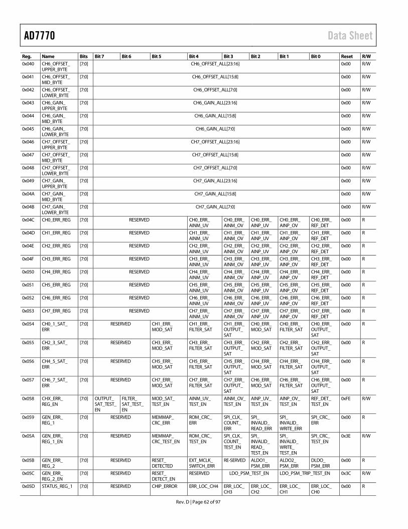
AD7770 Data Sheet
Rev. D | Page 62 of 97
Reg. Name Bits Bit 7 Bit 6 Bit 5 Bit 4 Bit 3 Bit 2 Bit 1 Bit 0 Reset R/W
0x040 CH6_OFFSET_ UPPER_BYTE
[7:0] CH6_OFFSET_ALL[23:16] 0x00 R/W
0x041 CH6_OFFSET_ MID_BYTE
[7:0] CH6_OFFSET_ALL[15:8] 0x00 R/W
0x042 CH6_OFFSET_ LOWER_BYTE
[7:0] CH6_OFFSET_ALL[7:0] 0x00 R/W
0x043 CH6_GAIN_ UPPER_BYTE
[7:0] CH6_GAIN_ALL[23:16] 0x00 R/W
0x044 CH6_GAIN_ MID_BYTE
[7:0] CH6_GAIN_ALL[15:8] 0x00 R/W
0x045 CH6_GAIN_ LOWER_BYTE
[7:0] CH6_GAIN_ALL[7:0] 0x00 R/W
0x046 CH7_OFFSET_ UPPER_BYTE
[7:0] CH7_OFFSET_ALL[23:16] 0x00 R/W
0x047 CH7_OFFSET_ MID_BYTE
[7:0] CH7_OFFSET_ALL[15:8] 0x00 R/W
0x048 CH7_OFFSET_ LOWER_BYTE
[7:0] CH7_OFFSET_ALL[7:0] 0x00 R/W
0x049 CH7_GAIN_ UPPER_BYTE
[7:0] CH7_GAIN_ALL[23:16] 0x00 R/W
0x04A CH7_GAIN_ MID_BYTE
[7:0] CH7_GAIN_ALL[15:8] 0x00 R/W
0x04B CH7_GAIN_ LOWER_BYTE
[7:0] CH7_GAIN_ALL[7:0] 0x00 R/W
0x04C CH0_ERR_REG [7:0] RESERVED CH0_ERR_ AINM_UV
CH0_ERR_ AINM_OV
CH0_ERR_ AINP_UV
CH0_ERR_ AINP_OV
CH0_ERR_ REF_DET
0x00 R
0x04D CH1_ERR_REG [7:0] RESERVED CH1_ERR_ AINM_UV
CH1_ERR_ AINM_OV
CH1_ERR_ AINP_UV
CH1_ERR_ AINP_OV
CH1_ERR_ REF_DET
0x00 R
0x04E CH2_ERR_REG [7:0] RESERVED CH2_ERR_ AINM_UV
CH2_ERR_ AINM_OV
CH2_ERR_ AINP_UV
CH2_ERR_ AINP_OV
CH2_ERR_ REF_DET
0x00 R
0x04F CH3_ERR_REG [7:0] RESERVED CH3_ERR_ AINM_UV
CH3_ERR_ AINM_OV
CH3_ERR_ AINP_UV
CH3_ERR_ AINP_OV
CH3_ERR_ REF_DET
0x00 R
0x050 CH4_ERR_REG [7:0] RESERVED CH4_ERR_ AINM_UV
CH4_ERR_ AINM_OV
CH4_ERR_ AINP_UV
CH4_ERR_ AINP_OV
CH4_ERR_ REF_DET
0x00 R
0x051 CH5_ERR_REG [7:0] RESERVED CH5_ERR_ AINM_UV
CH5_ERR_ AINM_OV
CH5_ERR_ AINP_UV
CH5_ERR_ AINP_OV
CH5_ERR_ REF_DET
0x00 R
0x052 CH6_ERR_REG [7:0] RESERVED CH6_ERR_ AINM_UV
CH6_ERR_ AINM_OV
CH6_ERR_ AINP_UV
CH6_ERR_ AINP_OV
CH6_ERR_ REF_DET
0x00 R
0x053 CH7_ERR_REG [7:0] RESERVED CH7_ERR_ AINM_UV
CH7_ERR_ AINM_OV
CH7_ERR_ AINP_UV
CH7_ERR_ AINP_OV
CH7_ERR_ REF_DET
0x00 R
0x054 CH0_1_SAT_ ERR
[7:0] RESERVED CH1_ERR_ MOD_SAT
CH1_ERR_ FILTER_SAT
CH1_ERR_ OUTPUT_ SAT
CH0_ERR_ MOD_SAT
CH0_ERR_ FILTER_SAT
CH0_ERR_ OUTPUT_ SAT
0x00 R
0x055 CH2_3_SAT_ ERR
[7:0] RESERVED CH3_ERR_ MOD_SAT
CH3_ERR_ FILTER_SAT
CH3_ERR_ OUTPUT_ SAT
CH2_ERR_ MOD_SAT
CH2_ERR_ FILTER_SAT
CH2_ERR_ OUTPUT_ SAT
0x00 R
0x056 CH4_5_SAT_ ERR
[7:0] RESERVED CH5_ERR_ MOD_SAT
CH5_ERR_ FILTER_SAT
CH5_ERR_ OUTPUT_ SAT
CH4_ERR_ MOD_SAT
CH4_ERR_ FILTER_SAT
CH4_ERR_ OUTPUT_ SAT
0x00 R
0x057 CH6_7_SAT_ ERR
[7:0] RESERVED CH7_ERR_ MOD_SAT
CH7_ERR_ FILTER_SAT
CH7_ERR_ OUTPUT_ SAT
CH6_ERR_ MOD_SAT
CH6_ERR_ FILTER_SAT
CH6_ERR_ OUTPUT_ SAT
0x00 R
0x058 CHX_ERR_ REG_EN
[7:0] OUTPUT_ SAT_TEST_EN
FILTER_ SAT_TEST_ EN
MOD_SAT_ TEST_EN
AINM_UV_ TEST_EN
AINM_OV_ TEST_EN
AINP_UV_ TEST_EN
AINP_OV_ TEST_EN
REF_DET_ TEST_EN
0xFE R/W
0x059 GEN_ERR_ REG_1
[7:0] RESERVED MEMMAP_ CRC_ERR
ROM_CRC_ ERR
SPI_CLK_ COUNT_ ERR
SPI_ INVALID_ READ_ERR
SPI_ INVALID_ WRITE_ERR
SPI_CRC_ ERR
0x00 R
0x05A GEN_ERR_ REG_1_EN
[7:0] RESERVED MEMMAP_ CRC_TEST_EN
ROM_CRC_ TEST_EN
SPI_CLK_ COUNT_ TEST_EN
SPI_ INVALID_ READ_ TEST_EN
SPI_ INVALID_ WRITE_ TEST_EN
SPI_CRC_ TEST_EN
0x3E R/W
0x05B GEN_ERR_ REG_2
[7:0] RESERVED RESET_ DETECTED
EXT_MCLK_ SWITCH_ERR
RE-SERVED ALDO1_ PSM_ERR
ALDO2_ PSM_ERR
DLDO_ PSM_ERR
0x00 R
0x05C GEN_ERR_ REG_2_EN
[7:0] RESERVED RESET_ DETECT_EN
RESERVED LDO_PSM_TEST_EN LDO_PSM_TRIP_TEST_EN 0x3C R/W
0x05D STATUS_REG_1 [7:0] RESERVED CHIP_ERROR ERR_LOC_CH4 ERR_LOC_CH3
ERR_LOC_ CH2
ERR_LOC_ CH1
ERR_LOC_ CH0
0x00 R

Data Sheet AD7770
Rev. D | Page 63 of 97
Reg. Name Bits Bit 7 Bit 6 Bit 5 Bit 4 Bit 3 Bit 2 Bit 1 Bit 0 Reset R/W
0x05E STATUS_REG_2 [7:0] RESERVED CHIP_ERROR ERR_LOC_ GEN2
ERR_LOC_ GEN1
ERR_ LOC_CH7
ERR_LOC_ CH6
ERR_LOC_ CH5
0x00 R
0x05F STATUS_REG_3 [7:0] RESERVED CHIP_ERROR INIT_ COMPLETE
ERR_LOC_ SAT_CH6_7
ERR_LOC_SAT_CH4_5
ERR_LOC_ SAT_CH2_3
ERR_LOC_ SAT_CH0_1
0x00 R
0x060 SRC_N_MSB [7:0] RESERVED SRC_N_ALL[11:8] 0x00 R/W
0x061 SRC_N_LSB [7:0] SRC_N_ALL[7:0] 0x80 R/W
0x062 SRC_IF_MSB [7:0] SRC_IF_ALL[15:8] 0x00 R/W
0x063 SRC_IF_LSB [7:0] SRC_IF_ALL[7:0] 0x00 R/W
0x064 SRC_UPDATE [7:0] SRC_ LOAD_ SOURCE
RESERVED SRC_LOAD_ UPDATE
0x00 R/W

AD7770 Data Sheet
Rev. D | Page 64 of 97
REGISTER DETAILS CHANNEL 0 CONFIGURATION REGISTER Address: 0x000, Reset: 0x00, Name: CH0_CONFIG
AFE Gain
11: Gain 8.10: Gain 4.01: Gain 2.00: Gain 1.
Channel used as Reference monitor
Channel Meter Mux RX Mode
0
01
02
03
04
05
06
07
0
[7:6] CH0_GAIN (R/W) [2:0] RESERVED
[5] CH0_REF_MONITOR (R/W)
[3] RESERVED
[4] CH0_RX (R/W)
Table 45. Bit Descriptions for CH0_CONFIG Bits Bit Name Settings Description Reset Access [7:6] CH0_GAIN AFE Gain 0x0 R/W 00 Gain = 1 01 Gain = 2 10 Gain = 4 11 Gain = 8 5 CH0_REF_MONITOR Channel Used as Reference Monitor 0x0 R/W 4 CH0_RX Channel Meter Mux Rx Mode 0x0 R/W [3:0] RESERVED Reserved 0x0 R/W
CHANNEL 1 CONFIGURATION REGISTER Address: 0x001, Reset: 0x00, Name: CH1_CONFIG
AFE Gain
11: Gain = 8.10: Gain = 4.01: Gain = 2.00: Gain = 1.
Channel used as Reference monitor
Channel Meter Mux RX Mode
0
01
02
03
04
05
06
07
0
[7:6] CH1_GAIN (R/W) [2:0] RESERVED
[5] CH1_REF_MONITOR (R/W)
[3] RESERVED
[4] CH1_RX (R/W)
Table 46. Bit Descriptions for CH1_CONFIG Bits Bit Name Settings Description Reset Access [7:6] CH1_GAIN AFE Gain 0x0 R/W 00 Gain = 1 01 Gain = 2 10 Gain = 4 11 Gain = 8 5 CH1_REF_MONITOR Channel Used as Reference Monitor 0x0 R/W 4 CH1_RX Channel Meter Mux Rx Mode 0x0 R/W [3:0] RESERVED Reserved 0x0 R/W
Data Sheet AD7770
Rev. D | Page 65 of 97
CHANNEL 2 CONFIGURATION REGISTER Address: 0x002, Reset: 0x00, Name: CH2_CONFIG
AFE Gain
11: Gain 8.10: Gain 4.01: Gain 2.00: Gain 1.
Channel used as Reference monitor
Channel Meter Mux RX Mode
0
01
02
03
04
05
06
07
0
[7:6] CH2_GAIN (R/W) [2:0] RESERVED
[5] CH2_REF_MONITOR (R/W)
[3] RESERVED
[4] CH2_RX (R/W)
Table 47. Bit Descriptions for CH2_CONFIG Bits Bit Name Settings Description Reset Access [7:6] CH2_GAIN AFE Gain 0x0 R/W 00 Gain = 1 01 Gain = 2 10 Gain = 4 11 Gain = 8 5 CH2_REF_MONITOR Channel Used as Reference Monitor 0x0 R/W 4 CH2_RX Channel Meter Mux Rx Mode 0x0 R/W [3:0] RESERVED Reserved 0x0 R/W
CHANNEL 3 CONFIGURATION REGISTER Address: 0x003, Reset: 0x00, Name: CH3_CONFIG
AFE Gain
11: Gain 8.10: Gain 4.01: Gain 2.00: Gain 1.
Channel used as Reference monitor
Channel Meter Mux RX Mode
0
01
02
03
04
05
06
07
0
[7:6] CH3_GAIN (R/W) [2:0] RESERVED
[5] CH3_REF_MONITOR (R/W)
[3] RESERVED
[4] CH3_RX (R/W)
Table 48. Bit Descriptions for CH3_CONFIG Bits Bit Name Settings Description Reset Access [7:6] CH3_GAIN AFE Gain 0x0 R/W 00 Gain = 1 01 Gain = 2 10 Gain = 4 11 Gain = 8 5 CH3_REF_MONITOR Channel Used as Reference Monitor 0x0 R/W 4 CH3_RX Channel Meter Mux Rx Mode 0x0 R/W [3:0] RESERVED Reserved 0x0 R/W

AD7770 Data Sheet
Rev. D | Page 66 of 97
CHANNEL 4 CONFIGURATION REGISTER Address: 0x004, Reset: 0x00, Name: CH4_CONFIG
AFE Gain
11: Gain 8.10: Gain 4.01: Gain 2.00: Gain 1.
Channel used as Reference monitor
Channel Meter Mux RX Mode
0
01
02
03
04
05
06
07
0
[7:6] CH4_GAIN (R/W) [2:0] RESERVED
[5] CH4_REF_MONITOR (R/W)
[3] RESERVED
[4] CH4_RX (R/W)
Table 49. Bit Descriptions for CH4_CONFIG Bits Bit Name Settings Description Reset Access [7:6] CH4_GAIN AFE Gain 0x0 R/W 00 Gain = 1 01 Gain = 2 10 Gain = 4 11 Gain = 8 5 CH4_REF_MONITOR Channel Used as Reference Monitor 0x0 R/W 4 CH4_RX Channel Meter Mux Rx Mode 0x0 R/W [3:0] RESERVED Reserved 0x0 R/W
CHANNEL 5 CONFIGURATION REGISTER Address: 0x005, Reset: 0x00, Name: CH5_CONFIG
AFE Gain
11: Gain 8.10: Gain 4.01: Gain 2.00: Gain 1.
Channel used as Reference monitor
Channel Meter Mux RX Mode
0
01
02
03
04
05
06
07
0
[7:6] CH5_GAIN (R/W) [2:0] RESERVED
[5] CH5_REF_MONITOR (R/W)
[3] RESERVED
[4] CH5_RX (R/W)
Table 50. Bit Descriptions for CH5_CONFIG Bits Bit Name Settings Description Reset Access [7:6] CH5_GAIN AFE Gain 0x0 R/W 00 Gain = 1 01 Gain = 2 10 Gain = 4 11 Gain = 8 5 CH5_REF_MONITOR Channel Used as Reference Monitor 0x0 R/W 4 CH5_RX Channel Meter Mux Rx Mode 0x0 R/W [3:0] RESERVED Reserved 0x0 R/W

Data Sheet AD7770
Rev. D | Page 67 of 97
CHANNEL 6 CONFIGURATION REGISTER Address: 0x006, Reset: 0x00, Name: CH6_CONFIG
AFE Gain
11: Gain 8.10: Gain 4.01: Gain 2.00: Gain 1.
Channel used as Reference monitor
Channel Meter Mux RX Mode
0
01
02
03
04
05
06
07
0
[7:6] CH6_GAIN (R/W) [2:0] RESERVED
[5] CH6_REF_MONITOR (R/W)
[3] RESERVED
[4] CH6_RX (R/W)
Table 51. Bit Descriptions for CH6_CONFIG Bits Bit Name Settings Description Reset Access [7:6] CH6_GAIN AFE Gain 0x0 R/W 00 Gain = 1 01 Gain = 2 10 Gain = 4 11 Gain = 8 5 CH6_REF_MONITOR Channel Used as Reference Monitor 0x0 R/W 4 CH6_RX Channel Meter Mux Rx Mode 0x0 R/W [3:0] RESERVED Reserved 0x0 R/W
CHANNEL 7 CONFIGURATION REGISTER Address: 0x007, Reset: 0x00, Name: CH7_CONFIG
AFE Gain
11: Gain 8.10: Gain 4.01: Gain 2.00: Gain 1.
Channel used as Reference monitor
Channel Meter Mux RX Mode
0
01
02
03
04
05
06
07
0
[7:6] CH7_GAIN (R/W) [2:0] RESERVED
[5] CH7_REF_MONITOR (R/W)
[3] RESERVED
[4] CH7_RX (R/W)
Table 52. Bit Descriptions for CH7_CONFIG Bits Bit Name Settings Description Reset Access [7:6] CH7_GAIN AFE Gain 0x0 R/W 00 Gain = 1 01 Gain = 2 10 Gain = 4 11 Gain = 8 5 CH7_REF_MONITOR Channel Used as Reference Monitor 0x0 R/W 4 CH7_RX Channel Meter Mux Rx Mode 0x0 R/W [3:0] RESERVED Reserved 0x0 R/W

AD7770 Data Sheet
Rev. D | Page 68 of 97
DISABLE CLOCKS TO ADC CHANNEL REGISTER Address: 0x008, Reset: 0x00, Name: CH_DISABLE
Channel 7 Disable Channel 0 Disable
Channel 6 Disable Channel 1 Disable
Channel 5 Disable Channel 2 Disable
Channel 4 Disable Channel 3 Disable
0
01
02
03
04
05
06
07
0
[7] CH7_DISABLE (R/W) [0] CH0_DISABLE (R/W)
[6] CH6_DISABLE (R/W) [1] CH1_DISABLE (R/W)
[5] CH5_DISABLE (R/W) [2] CH2_DISABLE (R/W)
[4] CH4_DISABLE (R/W) [3] CH3_DISABLE (R/W)
Table 53. Bit Descriptions for CH_DISABLE Bits Bit Name Settings Description Reset Access 7 CH7_DISABLE Channel 7 Disable 0x0 R/W 6 CH6_DISABLE Channel 6 Disable 0x0 R/W 5 CH5_DISABLE Channel 5 Disable 0x0 R/W 4 CH4_DISABLE Channel 4 Disable 0x0 R/W 3 CH3_DISABLE Channel 3 Disable 0x0 R/W 2 CH2_DISABLE Channel 2 Disable 0x0 R/W 1 CH1_DISABLE Channel 1 Disable 0x0 R/W 0 CH0_DISABLE Channel 0 Disable 0x0 R/W
CHANNEL 0 SYNC OFFSET REGISTER Address: 0x009, Reset: 0x00, Name: CH0_SYNC_OFFSET
Channel Sync Offset
0
01
02
03
04
05
06
07
0
[7:0] CH0_SYNC_OFFSET (R/W)
Table 54. Bit Descriptions for CH0_SYNC_OFFSET Bits Bit Name Settings Description Reset Access [7:0] CH0_SYNC_OFFSET Channel Sync Offset 0x0 R/W
CHANNEL 1 SYNC OFFSET REGISTER Address: 0x00A, Reset: 0x00, Name: CH1_SYNC_OFFSET
Channel Sync Offset
0
01
02
03
04
05
06
07
0
[7:0] CH1_SYNC_OFFSET (R/W)
Table 55. Bit Descriptions for CH1_SYNC_OFFSET Bits Bit Name Settings Description Reset Access [7:0] CH1_SYNC_OFFSET Channel Sync Offset 0x0 R/W
CHANNEL 2 SYNC OFFSET REGISTER Address: 0x00B, Reset: 0x00, Name: CH2_SYNC_OFFSET
Channel Sync Offset
0
01
02
03
04
05
06
07
0
[7:0] CH2_SYNC_OFFSET (R/W)
Table 56. Bit Descriptions for CH2_SYNC_OFFSET Bits Bit Name Settings Description Reset Access [7:0] CH2_SYNC_OFFSET Channel Sync Offset 0x0 R/W

Data Sheet AD7770
Rev. D | Page 69 of 97
CHANNEL 3 SYNC OFFSET REGISTER Address: 0x00C, Reset: 0x00, Name: CH3_SYNC_OFFSET
Channel Sync Offset
0
01
02
03
04
05
06
07
0
[7:0] CH3_SYNC_OFFSET (R/W)
Table 57. Bit Descriptions for CH3_SYNC_OFFSET Bits Bit Name Settings Description Reset Access [7:0] CH3_SYNC_OFFSET Channel Sync Offset 0x0 R/W
CHANNEL 4 SYNC OFFSET REGISTER Address: 0x00D, Reset: 0x00, Name: CH4_SYNC_OFFSET
Channel Sync Offset
0
01
02
03
04
05
06
07
0
[7:0] CH4_SYNC_OFFSET (R/W)
Table 58. Bit Descriptions for CH4_SYNC_OFFSET Bits Bit Name Settings Description Reset Access [7:0] CH4_SYNC_OFFSET Channel Sync Offset 0x0 R/W
CHANNEL 5 SYNC OFFSET REGISTER Address: 0x00E, Reset: 0x00, Name: CH5_SYNC_OFFSET
Channel Sync Offset
0
01
02
03
04
05
06
07
0
[7:0] CH5_SYNC_OFFSET (R/W)
Table 59. Bit Descriptions for CH5_SYNC_OFFSET Bits Bit Name Settings Description Reset Access [7:0] CH5_SYNC_OFFSET Channel Sync Offset 0x0 R/W
CHANNEL 6 SYNC OFFSET REGISTER Address: 0x00F, Reset: 0x00, Name: CH6_SYNC_OFFSET
Channel Sync Offset
0
01
02
03
04
05
06
07
0
[7:0] CH6_SYNC_OFFSET (R/W)
Table 60. Bit Descriptions for CH6_SYNC_OFFSET Bits Bit Name Settings Description Reset Access [7:0] CH6_SYNC_OFFSET Channel Sync Offset 0x0 R/W
CHANNEL 7 SYNC OFFSET REGISTER Address: 0x010, Reset: 0x00, Name: CH7_SYNC_OFFSET
Channel Sync Offset
0
01
02
03
04
05
06
07
0
[7:0] CH7_SYNC_OFFSET (R/W)
Table 61. Bit Descriptions for CH7_SYNC_OFFSET Bits Bit Name Settings Description Reset Access [7:0] CH7_SYNC_OFFSET Channel Sync Offset 0x0 R/W

AD7770 Data Sheet
Rev. D | Page 70 of 97
GENERAL USER CONFIGURATION 1 REGISTER Address: 0x011, Reset: 0x24, Name: GENERAL_USER_CONFIG_1
If all SD channels are disabled, settingthis bit high allows DCLK to continuetoggling
Soft Reset
11: 1st write.10: 2nd write.01: No Effect.00: No Effect.
Power Mode
1: High Resolution.0: Low Power (1/4)
PowerDown s ignal for internal oscillator.Active Low
PowerDown VCM Buffer. Active LowPowerDown SA. Active Low
PowerDown Internal Reference OutputBuffer. Active Low
0
01
02
13
04
05
16
07
0
[7] ALL_CH_DIS__MCLK_EN (R/W) [1:0] SOFT_RESET (R/W)
[6] POWERMODE (R/W)
[2] PDB_RC_OSC (R/W)
[5] PDB_VCM (R/W)[3] PDB_SAR (R/W)
[4] PDB_REFOUT_BUF (R/W)
Table 62. Bit Descriptions for GENERAL_USER_CONFIG_1 Bits Bit Name Settings Description Reset Access 7 ALL_CH_DIS_MCLK_EN If all Σ-Δ channels are disabled, setting this bit high allows DCLK to
continue toggling. 0x0 R/W
6 POWERMODE Power Mode. 0x0 R/W 0 Low power (1/4). 1 High resolution. 5 PDB_VCM Power Down VCM Buffer. Active low. 0x1 R/W 4 PDB_REFOUT_BUF Power Down Internal Reference Output Buffer. Active low. 0x0 R/W 3 PDB_SAR Power Down SAR. Active low. 0x0 R/W 2 PDB_RC_OSC Power Down Signal for Internal Oscillator. Active low. 0x1 R/W [1:0] SOFT_RESET Soft Reset. 0x0 R/W 00 No effect. 01 No effect. 10 2nd write. 11 1st write.
GENERAL USER CONFIGURATION 2 REGISTER Address: 0x012, Reset: 0x09, Name: GENERAL_USER_CONFIG_2
SYNC pulse generated thru SPI
1:STARTb pin in the control module.This bit is ANDed with the value on
0:
generate a pulse in /SYNC_IN pin.on STARTb pin in the control module,This s ignal is ANDed with the value
DOUT Drive Strength
11: Extra Strong.10: Weak.01: Strong.00: Nominal.
Sets SPI interface to read back SARresult on SDO
SDO Drive Strength
11: Extra Strong.10: Weak.01: Strong.00: Nominal.
0
11
02
03
14
05
06
07
0
[7] RESERVED [0] SPI_SYNC (R/W)
[6] RESERVED
[2:1] DOUT_DRIVE_STR (R/W)
[5] SAR_DIAG_MODE_EN (R/W)
[4:3] SDO_DRIVE_STR (R/W)
Table 63. Bit Descriptions for GENERAL_USER_CONFIG_2 Bits Bit Name Settings Description Reset Access [7:6] RESERVED Reserved. 0x0 R/W 5 SAR_DIAG_MODE_EN Sets SPI to Read Back SAR Result on SDO. 0x0 R/W

Data Sheet AD7770
Rev. D | Page 71 of 97
Bits Bit Name Settings Description Reset Access [4:3] SDO_DRIVE_STR SDO Drive Strength. 0x1 R/W 00 Nominal. 01 Strong. 10 Weak. 11 Extra strong. [2:1] DOUT_DRIVE_STR DOUTx Drive Strength. 0x0 R/W 00 Nominal. 01 Strong. 10 Weak. 11 Extra strong. 0 SPI_SYNC SYNC Pulse Generated Through SPI. 0x1 R/W 0 This signal is AND’ed with the value on the START pin in the control module
and generates a pulse in the SYNC_IN pin.
1 This bit is AND’ed with the value on START pin in the control module.
GENERAL USER CONFIGURATION 3 REGISTER Address: 0x013, Reset: 0x80, Name: GENERAL_USER_CONFIG_3
Disable deglitching of CONVST pin
11: No deglitch circuit.10: CONVST_SAR Deglitch 1.5 MCLK.01: Reserved.00: Reserved.
Disables the clock qualifier checkif the user requires to use an MCLKsignal < 265kHz.
Enable to SPI s lave mode to readback ADC on SDO
0
01
02
03
04
05
06
07
1
[7:6] CONVST_DEGLITCH_DIS (R/W) [0] CLK_QUAL_DIS (R/W)
[5] RESERVED
[1] RESERVED
[4] SPI_SLAVE_MODE_EN (R/W)
[3:2] RESERVED
Table 64. Bit Descriptions for GENERAL_USER_CONFIG_3 Bits Bit Name Settings Description Reset Access [7:6] CONVST_DEGLITCH_DIS Disable deglitching of CONVST_SAR pin. 0x2 R/W 00 Reserved. 01 Reserved. 10 CONVST_SAR deglitch 1.5/MCLK. 11 No deglitch circuit. 5 RESERVED Reserved. 0x0 R/W 4 SPI_SLAVE_MODE_EN Enable to SPI slave mode to read back ADC on SDO. 0x0 R/W [3:2] RESERVED Reserved. 0x0 R/W 1 RESERVED Reserved. 0x0 R/W 0 CLK_QUAL_DIS Disables the clock qualifier check if the user requires to use an MCLK
signal <265 kHz. 0x0 R/W

AD7770 Data Sheet
Rev. D | Page 72 of 97
DATA OUTPUT FORMAT REGISTER Address: 0x014, Reset: 0x20, Name: DOUT_FORMAT
Data out format
11: 1 DOUT Lines.10: 1 DOUT Lines.01: 2 DOUT Lines.00: 4 DOUT Lines.
Dout header format
1: CRC Header.0: Status Header.
Divide MCLK
111: Divide by 128.110: Divide by 64.101: Divide by 32.100: Divide by 16.011: Divide by 8.010: Divide by 4.001: Divide by 2.000: Divide by 1.
0
01
02
03
04
05
16
07
0
[7:6] DOUT_FORMAT (R/W) [0] RESERVED
[5] DOUT_HEADER_FORMAT (R/W)
[3:1] DCLK_CLK_DIV (R/W)
[4] RESERVED
Table 65. Bit Descriptions for DOUT_FORMAT Bits Bit Name Settings Description Reset Access [7:6] DOUT_FORMAT Data Out Format 0x0 R/W 00 4 DOUTx lines 01 2 DOUTx lines 10 1 DOUTx lines 11 1 DOUTx lines 5 DOUT_HEADER_FORMAT DOUTx Header Format 0x1 R/W 0 Status header 1 CRC header 4 RESERVED Reserved 0x0 R/W [3:1] DCLK_CLK_DIV Divide MCLK 0x0 R/W 000 Divide by 1 001 Divide by 2 010 Divide by 4 011 Divide by 8 100 Divide by 16 101 Divide by 32 110 Divide by 64 111 Divide by 128 0 RESERVED Reserved 0x0 R/W

Data Sheet AD7770
Rev. D | Page 73 of 97
MAIN ADC METER AND REFERENCE MUX CONTROL REGISTER Address: 0x015, Reset: 0x00, Name: ADC_MUX_CONFIG
SD ADC Reference Mux
11: External Reference REFx-/REFx+.10: External Supply AVDD1x/AVSSx.01: Internal Reference.00: External Reference REFx+/REFx-
SD ADC Meter Mux
1001: External Reference REFx+/REFx+.1000: Internal Reference +/+.0111: Internal Reference -/+.0110: Internal Reference +/-0101: External Reference REFx-/REFx-0100: External Reference REFx-/REFx+.0011: External Reference REFx+/REFx-0010: 280mV.
0
01
02
03
04
05
06
07
0
[7:6] REF_MUX_CTRL (R/W) [1:0] RESERVED
[5:2] MTR_MUX_CTRL (R/W)
Table 66. Bit Descriptions for ADC_MUX_CONFIG Bits Bit Name Settings Description Reset Access [7:6] REF_MUX_CTRL Σ-Δ ADC Reference Mux 0x0 R/W 00 External reference REFx+/REFx− 01 Internal reference. 10 External supply AVDD1x/AVSSx 11 External reference REFx−/REFx+ [5:2] MTR_MUX_CTRL Σ-Δ ADC Meter Mux 0x0 R/W 0010 280 mV 0011 External reference REFx+/REFx− 0100 External reference REFx−/REFx+ 0101 External reference REFx−/REFx− 0110 Internal reference +/− 0111 Internal reference −/+ 1000 Internal reference +/+ 1001 External reference REFx+/REFx+ [1:0] RESERVED Reserved 0x0 R/W

AD7770 Data Sheet
Rev. D | Page 74 of 97
GLOBAL DIAGNOSTICS MUX REGISTER Address: 0x016, Reset: 0x00, Name: GLOBAL_MUX_CONFIG
Global SAR diagnostics mux control
10101: AVSSx AVDD4. Attenuated.10100: REF2+ AVSSx.10011: REF1+ AVSSx.
...00010: REF1P REF1N.00001: DVBE AVSSx.00000: AUXAin+ AUXAin-
0
01
02
03
04
05
06
07
0
[7:3] GLOBAL_MUX_CTRL (R/W) [2:0] RESERVED
Table 67. Bit Descriptions for GLOBAL_MUX_CONFIG Bits Bit Name Settings Description Reset Access [7:3] GLOBAL_MUX_CTRL Global SAR Diagnostics Mux Control. 0x0 R/W 00000 AUXAIN+/AUXAIN−. 00001 DVBE/AVSSx. 00010 REF1+/REF1−. 00011 REF2+/REF2−. 00100 REF_OUT/AVSSx. 00101 VCM/AVSSx. 00110 AREG1CAP/AVSSx. 00111 AREG2CAP/AVSSx. 01000 DREGCAP/DGND. 01001 AVDD1A/AVSSx. 01010 AVDD1B/AVSSx. 01011 AVDD2A/AVSSx. 01100 AVDD2B/AVSSx. 01101 IOVDD/DGND. 01110 AVDD4/AVSSx. 01111 DGND/AVSSx. 10000 DGND/AVSSx. 10001 DGND/AVSSx. 10010 AVDD4/AVSSx. 10011 REF1+/AVSSx. 10100 REF2+/AVSSx. 10101 AVSSx/AVDD4. Attenuated. [2:0] RESERVED Reserved. 0x0 R/W
GPIO CONFIGURATION REGISTER Address: 0x017, Reset: 0x00, Name: GPIO_CONFIG
GPIO input/output
0
01
02
03
04
05
06
07
0
[7:3] RESERVED [2:0] GPIO_OP_EN (R/W)
Table 68. Bit Descriptions for GPIO_CONFIG Bits Bit Name Settings Description Reset Access [7:3] RESERVED Reserved 0x0 R/W [2:0] GPIO_OP_EN GPIO Input/Output 0x0 R/W

Data Sheet AD7770
Rev. D | Page 75 of 97
GPIO DATA REGISTER Address: 0x018, Reset: 0x00, Name: GPIO_DATA
Value sent to GPIO pins
Data read from GPIO pins
0
01
02
03
04
05
06
07
0
[7:6] RESERVED [2:0] GPIO_WRITE_DATA (R/W)
[5:3] GPIO_READ_DATA (R)
Table 69. Bit Descriptions for GPIO_DATA Bits Bit Name Settings Description Reset Access [7:6] RESERVED Reserved 0x0 R/W [5:3] GPIO_READ_DATA Data Read from the GPIO Pins 0x0 R [2:0] GPIO_WRITE_DATA Value Sent to the GPIO Pins 0x0 R/W
BUFFER CONFIGURATION 1 REGISTER Address: 0x019, Reset: 0x38, Name: BUFFER_CONFIG_1
Reference buffer positive enable Reference buffer negative enable
0
01
02
03
14
15
06
07
0
[7] RESERVED [0] RESERVED
[6] RESERVED [1] RESERVED
[5] RESERVED [2] RESERVED
[4] REF_BUF_POS_EN (R/W) [3] REF_BUF_NEG_EN (R/W)
Table 70. Bit Descriptions for BUFFER_CONFIG_1 Bits Bit Name Settings Description Reset Access [7:5] RESERVED Reserved 0x0 R/W 4 REF_BUF_POS_EN Reference Buffer Positive Enable 0x1 R/W 3 REF_BUF_NEG_EN Reference Buffer Negative Enable 0x1 R/W [2:0] RESERVED Reserved 0x0 R/W
BUFFER CONFIGURATION 2 REGISTER Address: 0x01A, Reset: 0xC0, Name: BUFFER_CONFIG_2
Reference buffer positive prechargeenable
DRegCap Overdrive Enable.
Reference buffer negative prechargeenable
AReg2Cap Overdrive Enable
AReg1Cap Overdrive Enable
0
01
02
03
04
05
06
17
1
[7] REFBUFP_PREQ (R/W) [0] PDB_DLDO_OVRDRV (R/W)
[6] REFBUFN_PREQ (R/W)[1] PDB_ALDO2_OVRDRV (R/W)
[5:3] RESERVED
[2] PDB_ALDO1_OVRDRV (R/W)
Table 71. Bit Descriptions for BUFFER_CONFIG_2 Bits Bit Name Settings Description Reset Access 7 REFBUFP_PREQ Reference Buffer Positive Precharge Enable 0x1 R/W 6 REFBUFN_PREQ Reference Buffer Negative Precharge Enable 0x1 R/W [5:3] RESERVED Reserved 0x0 R/W 2 PDB_ALDO1_OVRDRV AREG1CAP Overdrive Enable 0x0 R/W 1 PDB_ALDO2_OVRDRV AREG2CAP Overdrive Enable 0x0 R/W 0 PDB_DLDO_OVRDRV DREGCAP Overdrive Enable 0x0 R/W

AD7770 Data Sheet
Rev. D | Page 76 of 97
CHANNEL 0 OFFSET UPPER BYTE REGISTER Address: 0x01C, Reset: 0x00, Name: CH0_OFFSET_UPPER_BYTE
Combined Offset register Channel 0
0
01
02
03
04
05
06
07
0
[7:0] CH0_OFFSET_ALL[23:16] (R/W)
Table 72. Bit Descriptions for CH0_OFFSET_UPPER_BYTE Bits Bit Name Settings Description Reset Access [7:0] CH0_OFFSET_ALL[23:16] Combined Offset Register Channel 0 0x0 R/W
CHANNEL 0 OFFSET MIDDLE BYTE REGISTER Address: 0x01D, Reset: 0x00, Name: CH0_OFFSET_MID_BYTE
Combined Offset register Channel 0
0
01
02
03
04
05
06
07
0
[7:0] CH0_OFFSET_ALL[15:8] (R/W)
Table 73. Bit Descriptions for CH0_OFFSET_MID_BYTE Bits Bit Name Settings Description Reset Access [7:0] CH0_OFFSET_ALL[15:8] Combined Offset Register Channel 0 0x0 R/W
CHANNEL 0 OFFSET LOWER BYTE REGISTER Address: 0x01E, Reset: 0x00, Name: CH0_OFFSET_LOWER_BYTE
Combined Offset register Channel 0
0
01
02
03
04
05
06
07
0
[7:0] CH0_OFFSET_ALL[7:0] (R/W)
Table 74. Bit Descriptions for CH0_OFFSET_LOWER_BYTE Bits Bit Name Settings Description Reset Access [7:0] CH0_OFFSET_ALL[7:0] Combined Offset Register Channel 0 0x0 R/W
CHANNEL 0 GAIN UPPER BYTE REGISTER Address: 0x01F, Reset: 0x00, Name: CH0_GAIN_UPPER_BYTE
Combined gain register Channel 0
0
01
02
03
04
05
06
07
0
[7:0] CH0_GAIN_ALL[23:16] (R/W)
Table 75. Bit Descriptions for CH0_GAIN_UPPER_BYTE Bits Bit Name Settings Description Reset Access [7:0] CH0_GAIN_ALL[23:16] Combined Gain Register Channel 0 0x0 R/W
CHANNEL 0 GAIN MIDDLE BYTE REGISTER Address: 0x020, Reset: 0x00, Name: CH0_GAIN_MID_BYTE
Combined gain register Channel 0
0
01
02
03
04
05
06
07
0
[7:0] CH0_GAIN_ALL[15:8] (R/W)
Table 76. Bit Descriptions for CH0_GAIN_MID_BYTE Bits Bit Name Settings Description Reset Access [7:0] CH0_GAIN_ALL[15:8] Combined Gain Register Channel 0 0x0 R/W

Data Sheet AD7770
Rev. D | Page 77 of 97
CHANNEL 0 GAIN LOWER BYTE REGISTER Address: 0x021, Reset: 0x00, Name: CH0_GAIN_LOWER_BYTE
Combined gain register Channel 0
0
01
02
03
04
05
06
07
0
[7:0] CH0_GAIN_ALL[7:0] (R/W)
Table 77. Bit Descriptions for CH0_GAIN_LOWER_BYTE Bits Bit Name Settings Description Reset Access [7:0] CH0_GAIN_ALL[7:0] Combined Gain Register Channel 0 0x0 R/W
CHANNEL 1 OFFSET UPPER BYTE REGISTER Address: 0x022, Reset: 0x00, Name: CH1_OFFSET_UPPER_BYTE
Combined offset register Channel 1
0
01
02
03
04
05
06
07
0
[7:0] CH1_OFFSET_ALL[23:16] (R/W)
Table 78. Bit Descriptions for CH1_OFFSET_UPPER_BYTE Bits Bit Name Settings Description Reset Access [7:0] CH1_OFFSET_ALL[23:16] Combined Offset Register Channel 1 0x0 R/W
CHANNEL 1 OFFSET MIDDLE BYTE REGISTER Address: 0x023, Reset: 0x00, Name: CH1_OFFSET_MID_BYTE
Combined offset register Channel 1
0
01
02
03
04
05
06
07
0
[7:0] CH1_OFFSET_ALL[15:8] (R/W)
Table 79. Bit Descriptions for CH1_OFFSET_MID_BYTE Bits Bit Name Settings Description Reset Access [7:0] CH1_OFFSET_ALL[15:8] Combined Offset Register Channel 1 0x0 R/W
CHANNEL 1 OFFSET LOWER BYTE REGISTER Address: 0x024, Reset: 0x00, Name: CH1_OFFSET_LOWER_BYTE
Combined offset register Channel 1
0
01
02
03
04
05
06
07
0
[7:0] CH1_OFFSET_ALL[7:0] (R/W)
Table 80. Bit Descriptions for CH1_OFFSET_LOWER_BYTE Bits Bit Name Settings Description Reset Access [7:0] CH1_OFFSET_ALL[7:0] Combined Offset Register Channel 1 0x0 R/W

AD7770 Data Sheet
Rev. D | Page 78 of 97
CHANNEL 1 GAIN UPPER BYTE REGISTER Address: 0x025, Reset: 0x00, Name: CH1_GAIN_UPPER_BYTE
Combined gain register Channel 1
0
01
02
03
04
05
06
07
0
[7:0] CH1_GAIN_ALL[23:16] (R/W)
Table 81. Bit Descriptions for CH1_GAIN_UPPER_BYTE Bits Bit Name Settings Description Reset Access [7:0] CH1_GAIN_ALL[23:16] Combined Gain Register Channel 1 0x0 R/W
CHANNEL 1 GAIN MIDDLE BYTE REGISTER Address: 0x026, Reset: 0x00, Name: CH1_GAIN_MID_BYTE
Combined gain register Channel 1
0
01
02
03
04
05
06
07
0
[7:0] CH1_GAIN_ALL[15:8] (R/W)
Table 82. Bit Descriptions for CH1_GAIN_MID_BYTE Bits Bit Name Settings Description Reset Access [7:0] CH1_GAIN_ALL[15:8] Combined Gain Register Channel 1 0x0 R/W
CHANNEL 1 GAIN LOWER BYTE REGISTER Address: 0x027, Reset: 0x00, Name: CH1_GAIN_LOWER_BYTE
Combined gain register Channel 1
0
01
02
03
04
05
06
07
0
[7:0] CH1_GAIN_ALL[7:0] (R/W)
Table 83. Bit Descriptions for CH1_GAIN_LOWER_BYTE Bits Bit Name Settings Description Reset Access [7:0] CH1_GAIN_ALL[7:0] Combined Gain Register Channel 1 0x0 R/W
CHANNEL 2 OFFSET UPPER BYTE REGISTER Address: 0x028, Reset: 0x00, Name: CH2_OFFSET_UPPER_BYTE
Combined offset register Channel 2
0
01
02
03
04
05
06
07
0
[7:0] CH2_OFFSET_ALL[23:16] (R/W)
Table 84. Bit Descriptions for CH2_OFFSET_UPPER_BYTE Bits Bit Name Settings Description Reset Access [7:0] CH2_OFFSET_ALL[23:16] Combined Offset Register Channel 2 0x0 R/W
CHANNEL 2 OFFSET MIDDLE BYTE REGISTER Address: 0x029, Reset: 0x00, Name: CH2_OFFSET_MID_BYTE
Combined offset register Channel 2
0
01
02
03
04
05
06
07
0
[7:0] CH2_OFFSET_ALL[15:8] (R/W)
Table 85. Bit Descriptions for CH2_OFFSET_MID_BYTE Bits Bit Name Settings Description Reset Access [7:0] CH2_OFFSET_ALL[15:8] Combined Offset Register Channel 2 0x0 R/W

Data Sheet AD7770
Rev. D | Page 79 of 97
CHANNEL 2 OFFSET LOWER BYTE REGISTER Address: 0x02A, Reset: 0x00, Name: CH2_OFFSET_LOWER_BYTE
Combined offset register Channel 2
0
01
02
03
04
05
06
07
0
[7:0] CH2_OFFSET_ALL[7:0] (R/W)
Table 86. Bit Descriptions for CH2_OFFSET_LOWER_BYTE Bits Bit Name Settings Description Reset Access [7:0] CH2_OFFSET_ALL[7:0] Combined Offset Register Channel 2 0x0 R/W
CHANNEL 2 GAIN UPPER BYTE REGISTER Address: 0x02B, Reset: 0x00, Name: CH2_GAIN_UPPER_BYTE
Combined gain register Channel 2
0
01
02
03
04
05
06
07
0
[7:0] CH2_GAIN_ALL[23:16] (R/W)
Table 87. Bit Descriptions for CH2_GAIN_UPPER_BYTE Bits Bit Name Settings Description Reset Access [7:0] CH2_GAIN_ALL[23:16] Combined Gain Register Channel 2 0x0 R/W
CHANNEL 2 GAIN MIDDLE BYTE REGISTER Address: 0x02C, Reset: 0x00, Name: CH2_GAIN_MID_BYTE
Combined gain register Channel 2
0
01
02
03
04
05
06
07
0
[7:0] CH2_GAIN_ALL[15:8] (R/W)
Table 88. Bit Descriptions for CH2_GAIN_MID_BYTE Bits Bit Name Settings Description Reset Access [7:0] CH2_GAIN_ALL[15:8] Combined Gain Register Channel 2 0x0 R/W
CHANNEL 2 GAIN LOWER BYTE REGISTER Address: 0x02D, Reset: 0x00, Name: CH2_GAIN_LOWER_BYTE
Combined gain register Channel 2
0
01
02
03
04
05
06
07
0
[7:0] CH2_GAIN_ALL[7:0] (R/W)
Table 89. Bit Descriptions for CH2_GAIN_LOWER_BYTE Bits Bit Name Settings Description Reset Access [7:0] CH2_GAIN_ALL[7:0] Combined Gain Register Channel 2 0x0 R/W
CHANNEL 3 OFFSET UPPER BYTE REGISTER Address: 0x02E, Reset: 0x00, Name: CH3_OFFSET_UPPER_BYTE
Combined offset register Channel 3
0
01
02
03
04
05
06
07
0
[7:0] CH3_OFFSET_ALL[23:16] (R/W)
Table 90. Bit descriptions for CH3_OFFSET_UPPER_BYTE Bits Bit Name Settings Description Reset Access [7:0] CH3_OFFSET_ALL[23:16] Combined Offset Register Channel 3 0x0 R/W

AD7770 Data Sheet
Rev. D | Page 80 of 97
CHANNEL 3 OFFSET MIDDLE BYTE REGISTER Address: 0x02F, Reset: 0x00, Name: CH3_OFFSET_MID_BYTE
Combined offset register Channel 3
0
01
02
03
04
05
06
07
0
[7:0] CH3_OFFSET_ALL[15:8] (R/W)
Table 91. Bit Descriptions for CH3_OFFSET_MID_BYTE Bits Bit Name Settings Description Reset Access [7:0] CH3_OFFSET_ALL[15:8] Combined Offset Register Channel 3 0x0 R/W
CHANNEL 3 OFFSET LOWER BYTE REGISTER Address: 0x030, Reset: 0x00, Name: CH3_OFFSET_LOWER_BYTE
Combined offset register Channel 3
0
01
02
03
04
05
06
07
0
[7:0] CH3_OFFSET_ALL[7:0] (R/W)
Table 92. Bit Descriptions for CH3_OFFSET_LOWER_BYTE Bits Bit Name Settings Description Reset Access [7:0] CH3_OFFSET_ALL[7:0] Combined Offset Register Channel 3 0x0 R/W
CHANNEL 3 GAIN UPPER BYTE REGISTER Address: 0x031, Reset: 0x00, Name: CH3_GAIN_UPPER_BYTE
Combined gain register Channel 3
0
01
02
03
04
05
06
07
0
[7:0] CH3_GAIN_ALL[23:16] (R/W)
Table 93. Bit Descriptions for CH3_GAIN_UPPER_BYTE Bits Bit Name Settings Description Reset Access [7:0] CH3_GAIN_ALL[23:16] Combined Gain Register Channel 3 0x0 R/W
CHANNEL 3 GAIN MIDDLE BYTE REGISTER Address: 0x032, Reset: 0x00, Name: CH3_GAIN_MID_BYTE
Combined gain register Channel 3
0
01
02
03
04
05
06
07
0
[7:0] CH3_GAIN_ALL[15:8] (R/W)
Table 94. Bit Descriptions for CH3_GAIN_MID_BYTE Bits Bit Name Settings Description Reset Access [7:0] CH3_GAIN_ALL[15:8] Combined Gain Register Channel 3 0x0 R/W
CHANNEL 3 GAIN LOWER BYTE REGISTER Address: 0x033, Reset: 0x00, Name: CH3_GAIN_LOWER_BYTE
Combined gain register Channel 3
0
01
02
03
04
05
06
07
0
[7:0] CH3_GAIN_ALL[7:0] (R/W)
Table 95. Bit Descriptions for CH3_GAIN_LOWER_BYTE Bits Bit Name Settings Description Reset Access [7:0] CH3_GAIN_ALL[7:0] Combined Gain Register Channel 3 0x0 R/W

Data Sheet AD7770
Rev. D | Page 81 of 97
CHANNEL 4 OFFSET UPPER BYTE REGISTER Address: 0x034, Reset: 0x00, Name: CH4_OFFSET_UPPER_BYTE
Combined offset register Channel 4
0
01
02
03
04
05
06
07
0
[7:0] CH4_OFFSET_ALL[23:16] (R/W)
Table 96. Bit Descriptions for CH4_OFFSET_UPPER_BYTE Bits Bit Name Settings Description Reset Access [7:0] CH4_OFFSET_ALL[23:16] Combined Offset Register Channel 4 0x0 R/W
CHANNEL 4 OFFSET MIDDLE BYTE REGISTER Address: 0x035, Reset: 0x00, Name: CH4_OFFSET_MID_BYTE
Combined offset register Channel 4
0
01
02
03
04
05
06
07
0
[7:0] CH4_OFFSET_ALL[15:8] (R/W)
Table 97. Bit Descriptions for CH4_OFFSET_MID_BYTE Bits Bit Name Settings Description Reset Access [7:0] CH4_OFFSET_ALL[15:8] Combined Offset Register Channel 4 0x0 R/W
CHANNEL 4 OFFSET LOWER BYTE REGISTER Address: 0x036, Reset: 0x00, Name: CH4_OFFSET_LOWER_BYTE
Combined offset register Channel 4
0
01
02
03
04
05
06
07
0
[7:0] CH4_OFFSET_ALL[7:0] (R/W)
Table 98. Bit Descriptions for CH4_OFFSET_LOWER_BYTE Bits Bit Name Settings Description Reset Access [7:0] CH4_OFFSET_ALL[7:0] Combined Offset Register Channel 4 0x0 R/W
CHANNEL 4 GAIN UPPER BYTE REGISTER Address: 0x037, Reset: 0x00, Name: CH4_GAIN_UPPER_BYTE
Combined gain register Channel 4
0
01
02
03
04
05
06
07
0
[7:0] CH4_GAIN_ALL[23:16] (R/W)
Table 99. Bit Descriptions for CH4_GAIN_UPPER_BYTE Bits Bit Name Settings Description Reset Access [7:0] CH4_GAIN_ALL[23:16] Combined Gain Register Channel 4 0x0 R/W
CHANNEL 4 GAIN MIDDLE BYTE REGISTER Address: 0x038, Reset: 0x00, Name: CH4_GAIN_MID_BYTE
Combined gain register Channel 4
0
01
02
03
04
05
06
07
0
[7:0] CH4_GAIN_ALL[15:8] (R/W)
Table 100. Bit Descriptions for CH4_GAIN_MID_BYTE Bits Bit Name Settings Description Reset Access [7:0] CH4_GAIN_ALL[15:8] Combined Gain Register Channel 4 0x0 R/W

AD7770 Data Sheet
Rev. D | Page 82 of 97
CHANNEL 4 GAIN LOWER BYTE REGISTER Address: 0x039, Reset: 0x00, Name: CH4_GAIN_LOWER_BYTE
Combined gain register Channel 4
0
01
02
03
04
05
06
07
0
[7:0] CH4_GAIN_ALL[7:0] (R/W)
Table 101. Bit Descriptions for CH4_GAIN_LOWER_BYTE Bits Bit Name Settings Description Reset Access [7:0] CH4_GAIN_ALL[7:0] Combined Gain Register Channel 4 0x0 R/W
CHANNEL 5 OFFSET UPPER BYTE REGISTER Address: 0x03A, Reset: 0x00, Name: CH5_OFFSET_UPPER_BYTE
Combined offset register Channel 5
0
01
02
03
04
05
06
07
0
[7:0] CH5_OFFSET_ALL[23:16] (R/W)
Table 102. Bit Descriptions for CH5_OFFSET_UPPER_BYTE Bits Bit Name Settings Description Reset Access [7:0] CH5_OFFSET_ALL[23:16] Combined Offset Register Channel 5 0x0 R/W
CHANNEL 5 OFFSET MIDDLE BYTE REGISTER Address: 0x03B, Reset: 0x00, Name: CH5_OFFSET_MID_BYTE
Combined offset register Channel 5
0
01
02
03
04
05
06
07
0
[7:0] CH5_OFFSET_ALL[15:8] (R/W)
Table 103. Bit Descriptions for CH5_OFFSET_MID_BYTE Bits Bit Name Settings Description Reset Access [7:0] CH5_OFFSET_ALL[15:8] Combined Offset Register Channel 5 0x0 R/W
CHANNEL 5 OFFSET LOWER BYTE REGISTER Address: 0x03C, Reset: 0x00, Name: CH5_OFFSET_LOWER_BYTE
Combined offset register Channel 5
0
01
02
03
04
05
06
07
0
[7:0] CH5_OFFSET_ALL[7:0] (R/W)
Table 104. Bit Descriptions for CH5_OFFSET_LOWER_BYTE Bits Bit Name Settings Description Reset Access [7:0] CH5_OFFSET_ALL[7:0] Combined Offset Register Channel 5 0x0 R/W
CHANNEL 5 GAIN UPPER BYTE REGISTER Address: 0x03D, Reset: 0x00, Name: CH5_GAIN_UPPER_BYTE
Combined gain register Channel 5
0
01
02
03
04
05
06
07
0
[7:0] CH5_GAIN_ALL[23:16] (R/W)
Table 105. Bit Descriptions for CH5_GAIN_UPPER_BYTE Bits Bit Name Settings Description Reset Access [7:0] CH5_GAIN_ALL[23:16] Combined Gain Register Channel 5 0x0 R/W

Data Sheet AD7770
Rev. D | Page 83 of 97
CHANNEL 5 GAIN MIDDLE BYTE REGISTER Address: 0x03E, Reset: 0x00, Name: CH5_GAIN_MID_BYTE
Combined gain register Channel 5
0
01
02
03
04
05
06
07
0
[7:0] CH5_GAIN_ALL[15:8] (R/W)
Table 106. Bit Descriptions for CH5_GAIN_MID_BYTE Bits Bit Name Settings Description Reset Access [7:0] CH5_GAIN_ALL[15:8] Combined Gain Register Channel 5 0x0 R/W
CHANNEL 5 GAIN LOWER BYTE REGISTER Address: 0x03F, Reset: 0x00, Name: CH5_GAIN_LOWER_BYTE
Combined gain register Channel 5
0
01
02
03
04
05
06
07
0
[7:0] CH5_GAIN_ALL[7:0] (R/W)
Table 107. Bit Descriptions for CH5_GAIN_LOWER_BYTE Bits Bit Name Settings Description Reset Access [7:0] CH5_GAIN_ALL[7:0] Combined Gain Register Channel 5 0x0 R/W
CHANNEL 6 OFFSET UPPER BYTE REGISTER Address: 0x040, Reset: 0x00, Name: CH6_OFFSET_UPPER_BYTE
Combined offset register Channel 6
0
01
02
03
04
05
06
07
0
[7:0] CH6_OFFSET_ALL[23:16] (R/W)
Table 108. Bit Descriptions for CH6_OFFSET_UPPER_BYTE Bits Bit Name Settings Description Reset Access [7:0] CH6_OFFSET_ALL[23:16] Combined Offset Register Channel 6 0x0 R/W
CHANNEL 6 OFFSET MIDDLE BYTE REGISTER Address: 0x041, Reset: 0x00, Name: CH6_OFFSET_MID_BYTE
Combined offset register Channel 6
0
01
02
03
04
05
06
07
0
[7:0] CH6_OFFSET_ALL[15:8] (R/W)
Table 109. Bit Descriptions for CH6_OFFSET_MID_BYTE Bits Bit Name Settings Description Reset Access [7:0] CH6_OFFSET_ALL[15:8] Combined Offset Register Channel 6 0x0 R/W
CHANNEL 6 OFFSET LOWER BYTE REGISTER Address: 0x042, Reset: 0x00, Name: CH6_OFFSET_LOWER_BYTE
Combined offset register Channel 6
0
01
02
03
04
05
06
07
0
[7:0] CH6_OFFSET_ALL[7:0] (R/W)
Table 110. Bit Descriptions for CH6_OFFSET_LOWER_BYTE Bits Bit Name Settings Description Reset Access [7:0] CH6_OFFSET_ALL[7:0] Combined Offset Register Channel 6 0x0 R/W

AD7770 Data Sheet
Rev. D | Page 84 of 97
CHANNEL 6 GAIN UPPER BYTE REGISTER Address: 0x043, Reset: 0x00, Name: CH6_GAIN_UPPER_BYTE
Combined gain register Channel 6
0
01
02
03
04
05
06
07
0
[7:0] CH6_GAIN_ALL[23:16] (R/W)
Table 111. Bit Descriptions for CH6_GAIN_UPPER_BYTE Bits Bit Name Settings Description Reset Access [7:0] CH6_GAIN_ALL[23:16] Combined Gain Register Channel 6 0x0 R/W
CHANNEL 6 GAIN MIDDLE BYTE REGISTER Address: 0x044, Reset: 0x00, Name: CH6_GAIN_MID_BYTE
Combined gain register Channel 6
0
01
02
03
04
05
06
07
0
[7:0] CH6_GAIN_ALL[15:8] (R/W)
Table 112. Bit Descriptions for CH6_GAIN_MID_BYTE Bits Bit Name Settings Description Reset Access [7:0] CH6_GAIN_ALL[15:8] Combined Gain Register Channel 6 0x0 R/W
CHANNEL 6 GAIN LOWER BYTE REGISTER Address: 0x045, Reset: 0x00, Name: CH6_GAIN_LOWER_BYTE
Combined gain register Channel 6
0
01
02
03
04
05
06
07
0
[7:0] CH6_GAIN_ALL[7:0] (R/W)
Table 113. Bit Descriptions for CH6_GAIN_LOWER_BYTE Bits Bit Name Settings Description Reset Access [7:0] CH6_GAIN_ALL[7:0] Combined Gain Register Channel 6 0x0 R/W
CHANNEL 7 OFFSET UPPER BYTE REGISTER Address: 0x046, Reset: 0x00, Name: CH7_OFFSET_UPPER_BYTE
Combined offset register Channel 7
0
01
02
03
04
05
06
07
0
[7:0] CH7_OFFSET_ALL[23:16] (R/W)
Table 114. Bit Descriptions for CH7_OFFSET_UPPER_BYTE Bits Bit Name Settings Description Reset Access [7:0] CH7_OFFSET_ALL[23:16] Combined Offset Register Channel 7 0x0 R/W
CHANNEL 7 OFFSET MIDDLE BYTE REGISTER Address: 0x047, Reset: 0x00, Name: CH7_OFFSET_MID_BYTE
Combined offset register Channel 7
0
01
02
03
04
05
06
07
0
[7:0] CH7_OFFSET_ALL[15:8] (R/W)
Table 115. Bit Descriptions for CH7_OFFSET_MID_BYTE Bits Bit Name Settings Description Reset Access [7:0] CH7_OFFSET_ALL[15:8] Combined Offset Register Channel 7 0x0 R/W

Data Sheet AD7770
Rev. D | Page 85 of 97
CHANNEL 7 OFFSET LOWER BYTE REGISTER Address: 0x048, Reset: 0x00, Name: CH7_OFFSET_LOWER_BYTE
Combined offset register Channel 7
0
01
02
03
04
05
06
07
0
[7:0] CH7_OFFSET_ALL[7:0] (R/W)
Table 116. Bit Descriptions for CH7_OFFSET_LOWER_BYTE Bits Bit Name Settings Description Reset Access [7:0] CH7_OFFSET_ALL[7:0] Combined Offset Register Channel 7 0x0 R/W
CHANNEL 7 GAIN UPPER BYTE REGISTER Address: 0x049, Reset: 0x00, Name: CH7_GAIN_UPPER_BYTE
Combined gain register Channel 7
0
01
02
03
04
05
06
07
0
[7:0] CH7_GAIN ALL[23:16] (R/W)
Table 117. Bit Descriptions for CH7_GAIN_UPPER_BYTE Bits Bit Name Settings Description Reset Access [7:0] CH7_GAIN ALL[23:16] Combined Gain Register Channel 7 0x0 R/W
CHANNEL 7 GAIN MIDDLE BYTE REGISTER Address: 0x04A, Reset: 0x00, Name: CH7_GAIN_MID_BYTE
Combined gain register Channel 7
0
01
02
03
04
05
06
07
0
[7:0] CH7_GAIN ALL[15:8] (R/W)
Table 118. Bit Descriptions for CH7_GAIN_MID_BYTE Bits Bit Name Settings Description Reset Access [7:0] CH7_GAIN ALL[15:8] Combined Gain Register Channel 7 0x0 R/W
CHANNEL 7 GAIN LOWER BYTE REGISTER Address: 0x04B, Reset: 0x00, Name: CH7_GAIN_LOWER_BYTE
Combined gain register Channel 7
0
01
02
03
04
05
06
07
0
[7:0] CH7_GAIN ALL[7:0] (R/W)
Table 119. Bit Descriptions for CH7_GAIN_LOWER_BYTE Bits Bit Name Settings Description Reset Access [7:0] CH7_GAIN ALL[7:0] Combined Gain Register Channel 7 0x0 R/W

AD7770 Data Sheet
Rev. D | Page 86 of 97
CHANNEL 0 STATUS REGISTER Address: 0x04C, Reset: 0x00, Name: CH0_ERR_REG
Channel 0 - Reference detect error
AIN0- undervoltage errorAIN0+ overvoltage error
AIN0- overvoltage errorAIN0+ undervoltage error
0
01
02
03
04
05
06
07
0
[7:5] RESERVED [0] CH0_ERR_REF_DET (R)
[4] CH0_ERR_AINM_UV (R)[1] CH0_ERR_AINP_OV (R)
[3] CH0_ERR_AINM_OV (R)[2] CH0_ERR_AINP_UV (R)
Table 120. Bit Descriptions for CH0_ERR_REG Bits Bit Name Settings Description Reset Access [7:5] RESERVED Reserved 0x0 R/W 4 CH0_ERR_AINM_UV Channel 0—AIN0− Undervoltage Error 0x0 R 3 CH0_ERR_AINM_OV Channel 0—AIN0− Overvoltage Error 0x0 R 2 CH0_ERR_AINP_UV Channel 0—AIN0+ Undervoltage Error 0x0 R 1 CH0_ERR_AINP_OV Channel 0—AIN0+ Overvoltage Error 0x0 R 0 CH0_ERR_REF_DET Channel 0—Reference Detect Error 0x0 R
CHANNEL 1 STATUS REGISTER Address: 0x04D, Reset: 0x00, Name: CH1_ERR_REG
Channel 1 - Reference detect error
AIN1- undervoltage errorAIN1+ overvoltage error
AIN1- overvoltage errorAIN1+ undervoltage error
0
01
02
03
04
05
06
07
0
[7:5] RESERVED [0] CH1_ERR_REF_DET (R)
[4] CH1_ERR_AINM_UV (R)[1] CH1_ERR_AINP_OV (R)
[3] CH1_ERR_AINM_OV (R)[2] CH1_ERR_AINP_UV (R)
Table 121. Bit Descriptions for CH1_ERR_REG Bits Bit Name Settings Description Reset Access [7:5] RESERVED Reserved 0x0 R/W 4 CH1_ERR_AINM_UV Channel 1—AIN1− Undervoltage Error 0x0 R 3 CH1_ERR_AINM_OV Channel 1—AIN1− Overvoltage Error 0x0 R 2 CH1_ERR_AINP_UV Channel 1—AIN1+ Undervoltage Error 0x0 R 1 CH1_ERR_AINP_OV Channel 1—AIN1+ Overvoltage Error 0x0 R 0 CH1_ERR_REF_DET Channel 1—Reference Detect Error 0x0 R
Data Sheet AD7770
Rev. D | Page 87 of 97
CHANNEL 2 STATUS REGISTER Address: 0x04E, Reset: 0x00, Name: CH2_ERR_REG
Channel 2 - Reference detect error
AIN2- undervoltage errorAIN2+ overvoltage error
AIN2- overvoltage errorAIN2+ undervoltage error
0
01
02
03
04
05
06
07
0
[7:5] RESERVED [0] CH2_ERR_REF_DET (R)
[4] CH2_ERR_AINM_UV (R)[1] CH2_ERR_AINP_OV (R)
[3] CH2_ERR_AINM_OV (R)[2] CH2_ERR_AINP_UV (R)
Table 122. Bit Descriptions for CH2_ERR_REG Bits Bit Name Settings Description Reset Access [7:5] RESERVED Reserved 0x0 R/W 4 CH2_ERR_AINM_UV Channel 2—AIN2− Undervoltage Error 0x0 R 3 CH2_ERR_AINM_OV Channel 2—AIN2− Overvoltage Error 0x0 R 2 CH2_ERR_AINP_UV Channel 2—AIN2+ Undervoltage Error 0x0 R 1 CH2_ERR_AINP_OV Channel 2—AIN2+ Overvoltage Error 0x0 R 0 CH2_ERR_REF_DET Channel 2—Reference Detect Error 0x0 R
CHANNEL 3 STATUS REGISTER Address: 0x04F, Reset: 0x00, Name: CH3_ERR_REG
Channel 3 - Reference detect error
AIN3- undervoltage errorAIN3+ overvoltage error
AIN3- overvoltage errorAIN3+ undervoltage error
0
01
02
03
04
05
06
07
0
[7:5] RESERVED [0] CH3_ERR_REF_DET (R)
[4] CH3_ERR_AINM_UV (R)[1] CH3_ERR_AINP_OV (R)
[3] CH3_ERR_AINM_OV (R)[2] CH3_ERR_AINP_UV (R)
Table 123. Bit Descriptions for CH3_ERR_REG Bits Bit Name Settings Description Reset Access [7:5] RESERVED Reserved 0x0 R/W 4 CH3_ERR_AINM_UV Channel 3—AIN3− Undervoltage Error 0x0 R 3 CH3_ERR_AINM_OV Channel 3—AIN3− Overvoltage Error 0x0 R 2 CH3_ERR_AINP_UV Channel 3—AIN3+ Undervoltage Error 0x0 R 1 CH3_ERR_AINP_OV Channel 3—AIN3+ Overvoltage Error 0x0 R 0 CH3_ERR_REF_DET Channel 3—Reference Detect Error 0x0 R

AD7770 Data Sheet
Rev. D | Page 88 of 97
CHANNEL 4 STATUS REGISTER Address: 0x050, Reset: 0x00, Name: CH4_ERR_REG
Channel 4 - Reference detect error
AIN4- undervoltage errorAIN4+ overvoltage error
AIN4- overvoltage errorAIN4+ undervoltage error
0
01
02
03
04
05
06
07
0
[7:5] RESERVED [0] CH4_ERR_REF_DET (R)
[4] CH4_ERR_AINM_UV (R)[1] CH4_ERR_AINP_OV (R)
[3] CH4_ERR_AINM_OV (R)[2] CH4_ERR_AINP_UV (R)
Table 124. Bit Descriptions for CH4_ERR_REG Bits Bit Name Settings Description Reset Access [7:5] RESERVED Reserved 0x0 R/W 4 CH4_ERR_AINM_UV Channel 4—AIN4− Undervoltage Error 0x0 R 3 CH4_ERR_AINM_OV Channel 4—AIN4− Overvoltage Error 0x0 R 2 CH4_ERR_AINP_UV Channel 4—AIN4+ Undervoltage Error 0x0 R 1 CH4_ERR_AINP_OV Channel 4—AIN4+ Overvoltage Error 0x0 R 0 CH4_ERR_REF_DET Channel 4—Reference Detect Error 0x0 R
CHANNEL 5 STATUS REGISTER Address: 0x051, Reset: 0x00, Name: CH5_ERR_REG
Channel 5 - Reference detect error
AIN5- undervoltage errorAIN5+ overvoltage error
AIN5- overvoltage errorAIN5+ undervoltage error
0
01
02
03
04
05
06
07
0
[7:5] RESERVED [0] CH5_ERR_REF_DET (R)
[4] CH5_ERR_AINM_UV (R)[1] CH5_ERR_AINP_OV (R)
[3] CH5_ERR_AINM_OV (R)[2] CH5_ERR_AINP_UV (R)
Table 125. Bit Descriptions for CH5_ERR_REG Bits Bit Name Settings Description Reset Access [7:5] RESERVED Reserved 0x0 R/W 4 CH5_ERR_AINM_UV Channel 5—AIN5− Undervoltage Error 0x0 R 3 CH5_ERR_AINM_OV Channel 5—AIN5− Overvoltage Error 0x0 R 2 CH5_ERR_AINP_UV Channel 5—AIN5+ Undervoltage Error 0x0 R 1 CH5_ERR_AINP_OV Channel 5—AIN5+ Overvoltage Error 0x0 R 0 CH5_ERR_REF_DET Channel 5—Reference Detect Error 0x0 R

Data Sheet AD7770
Rev. D | Page 89 of 97
CHANNEL 6 STATUS REGISTER Address: 0x052, Reset: 0x00, Name: CH6_ERR_REG
Channel 6 - Reference detect error
AIN6- undervoltage errorAIN6+ overvoltage error
AIN6- overvoltage errorAIN6+ undervoltage error
0
01
02
03
04
05
06
07
0
[7:5] RESERVED [0] CH6_ERR_REF_DET (R)
[4] CH6_ERR_AINM_UV (R)[1] CH6_ERR_AINP_OV (R)
[3] CH6_ERR_AINM_OV (R)[2] CH6_ERR_AINP_UV (R)
Table 126. Bit Descriptions for CH6_ERR_REG Bits Bit Name Settings Description Reset Access [7:5] RESERVED Reserved 0x0 R/W 4 CH6_ERR_AINM_UV Channel 6—AIN6− Undervoltage Error 0x0 R 3 CH6_ERR_AINM_OV Channel 6—AIN6− Overvoltage Error 0x0 R 2 CH6_ERR_AINP_UV Channel 6—AIN6+ Undervoltage Error 0x0 R 1 CH6_ERR_AINP_OV Channel 6—AIN6+ Overvoltage Error 0x0 R 0 CH6_ERR_REF_DET Channel 6—Reference Detect Error 0x0 R
CHANNEL 7 STATUS REGISTER Address: 0x053, Reset: 0x00, Name: CH7_ERR_REG
Channel 7 - Reference detect error
AIN7- undervoltage errorAIN7+ overvoltage error
AIN7- overvoltage errorAIN7+ undervoltage error
0
01
02
03
04
05
06
07
0
[7:5] RESERVED [0] CH7_ERR_REF_DET (R)
[4] CH7_ERR_AINM_UV (R)[1] CH7_ERR_AINP_OV (R)
[3] CH7_ERR_AINM_OV (R)[2] CH7_ERR_AINP_UV (R)
Table 127. Bit Descriptions for CH7_ERR_REG Bits Bit Name Settings Description Reset Access [7:5] RESERVED Reserved 0x0 R 4 CH7_ERR_AINM_UV Channel 7—AIN7− Undervoltage Error 0x0 R 3 CH7_ERR_AINM_OV Channel 7—AIN7− Overvoltage Error 0x0 R 2 CH7_ERR_AINP_UV Channel 7—AIN7+ Undervoltage Error 0x0 R 1 CH7_ERR_AINP_OV Channel 7—AIN7+ Overvoltage Error 0x0 R 0 CH7_ERR_REF_DET Channel 7—Reference Detect Error 0x0 R

AD7770 Data Sheet
Rev. D | Page 90 of 97
CHANNEL 0/CHANNEL 1 DSP ERRORS REGISTER Address: 0x054, Reset: 0x00, Name: CH0_1_SAT_ERR
Channel 0 - ADC convers ion hasexceeded lim its and has been clamped
Channel 1 - Modulator output saturationerror
Channel 0 - Filter result has exceededa reasonable level, before offset andgain calibration has been applied.Channel 1 - Filter result has exceeded
a reasonable level, before offset andgain calibration has been applied.
Channel 0 - Modulator output saturationerror
Channel 1 - ADC convers ion hasexceeded lim its and has been clamped
0
01
02
03
04
05
06
07
0
[7:6] RESERVED [0] CH0_ERR_OUTPUT_SAT (R)
[5] CH1_ERR_MOD_SAT (R)
[1] CH0_ERR_FILTER_SAT (R)
[4] CH1_ERR_FILTER_SAT (R)
[2] CH0_ERR_MOD_SAT (R)
[3] CH1_ERR_OUTPUT_SAT (R)
Table 128. Bit Descriptions for CH0_1_SAT_ERR Bits Bit Name Settings Description Reset Access [7:6] RESERVED Reserved 0x0 R 5 CH1_ERR_MOD_SAT Channel 1—Modulator output saturation error 0x0 R 4 CH1_ERR_FILTER_SAT Channel 1—Filter result has exceeded a reasonable level, before offset and
gain calibration are applied 0x0 R
3 CH1_ERR_OUTPUT_SAT Channel 1—ADC conversion has exceeded limits and is clamped 0x0 R 2 CH0_ERR_MOD_SAT Channel 0—Modulator output saturation error 0x0 R 1 CH0_ERR_FILTER_SAT Channel 0—Filter result has exceeded a reasonable level, before offset and
gain calibration are applied 0x0 R
0 CH0_ERR_OUTPUT_SAT Channel 0—ADC conversion has exceeded limits and is clamped 0x0 R
CHANNEL 2/CHANNEL 3 DSP ERRORS REGISTER Address: 0x055, Reset: 0x00, Name: CH2_3_SAT_ERR
Channel 2 - ADC convers ion hasexceeded lim its and has been clamped
Channel 3 - Modulator output saturationerror
Channel 2 - Filter result has exceededa reasonable level, before offset andgain calibration has been applied.Channel 3 - Filter result has exceeded
a reasonable level, before offset andgain calibration has been applied.
Channel 2 - Modulator output saturationerror
Channel 3 - ADC convers ion hasexceeded lim its and has been clamped
0
01
02
03
04
05
06
07
0
[7:6] RESERVED [0] CH2_ERR_OUTPUT_SAT (R)
[5] CH3_ERR_MOD_SAT (R)
[1] CH2_ERR_FILTER_SAT (R)
[4] CH3_ERR_FILTER_SAT (R)
[2] CH2_ERR_MOD_SAT (R)
[3] CH3_ERR_OUTPUT_SAT (R)
Table 129. Bit Descriptions for CH2_3_SAT_ERR Bits Bit Name Settings Description Reset Access [7:6] RESERVED Reserved 0x0 R 5 CH3_ERR_MOD_SAT Channel 3—Modulator output saturation error 0x0 R 4 CH3_ERR_FILTER_SAT Channel 3—Filter result has exceeded a reasonable level, before offset and
gain calibration are applied 0x0 R
3 CH3_ERR_OUTPUT_SAT Channel 3—ADC conversion has exceeded limits and is clamped 0x0 R 2 CH2_ERR_MOD_SAT Channel 2—Modulator output saturation error 0x0 R 1 CH2_ERR_FILTER_SAT Channel 2—Filter result has exceeded a reasonable level, before offset and
gain calibration are applied 0x0 R
0 CH2_ERR_OUTPUT_SAT Channel 2—ADC conversion has exceeded limits andis clamped 0x0 R

Data Sheet AD7770
Rev. D | Page 91 of 97
CHANNEL 4/CHANNEL 5 DSP ERRORS REGISTER Address: 0x056, Reset: 0x00, Name: CH4_5_SAT_ERR
Channel 4 - ADC convers ion hasexceeded lim its and has been clamped
Channel 5 - Modulator output saturationerror
Channel 4 - Filter result has exceededa reasonable level, before offset andgain calibration has been applied.Channel 5 - Filter result has exceeded
a reasonable level, before offset andgain calibration has been applied.
Channel 4 - Modulator output saturationerror
Channel 5 - ADC convers ion hasexceeded lim its and has been clamped
0
01
02
03
04
05
06
07
0
[7:6] RESERVED [0] CH4_ERR_OUTPUT_SAT (R)
[5] CH5_ERR_MOD_SAT (R)
[1] CH4_ERR_FILTER_SAT (R)
[4] CH5_ERR_FILTER_SAT (R)
[2] CH4_ERR_MOD_SAT (R)
[3] CH5_ERR_OUTPUT_SAT (R)
Table 130. Bit Descriptions for CH4_5_SAT_ERR Bits Bit Name Settings Description Reset Access [7:6] RESERVED Reserved 0x0 R 5 CH5_ERR_MOD_SAT Channel 5—Modulator output saturation error 0x0 R 4 CH5_ERR_FILTER_SAT Channel 5—Filter result has exceeded a reasonable level, before offset and
gain calibration are applied 0x0 R
3 CH5_ERR_OUTPUT_SAT Channel 5—ADC conversion has exceeded limits and is clamped 0x0 R 2 CH4_ERR_MOD_SAT Channel 4—Modulator output saturation error 0x0 R 1 CH4_ERR_FILTER_SAT Channel 4—Filter result has exceeded a reasonable level, before offset and
gain calibration are applied 0x0 R
0 CH4_ERR_OUTPUT_SAT Channel 4—ADC conversion has exceeded limits and is clamped 0x0 R
CHANNEL 6/CHANNEL 7 DSP ERRORS REGISTER Address: 0x057, Reset: 0x00, Name: CH6_7_SAT_ERR
Channel 6 - ADC convers ion hasexceeded lim its and has been clamped
Channel 7 - Modulator output saturationerror
Channel 6 - Filter result has exceededa reasonable level, before offset andgain calibration has been applied.Channel 7 - Filter result has exceeded
a reasonable level, before offset andgain calibration has been applied.
Channel 6 - Modulator output saturationerror
Channel 7 - ADC convers ion hasexceeded lim its and has been clamped
0
01
02
03
04
05
06
07
0
[7:6] RESERVED [0] CH6_ERR_OUTPUT_SAT (R)
[5] CH7_ERR_MOD_SAT (R)
[1] CH6_ERR_FILTER_SAT (R)
[4] CH7_ERR_FILTER_SAT (R)
[2] CH6_ERR_MOD_SAT (R)
[3] CH7_ERR_OUTPUT_SAT (R)
Table 131. Bit descriptions for CH6_7_SAT_ERR Bits Bit Name Settings Description Reset Access [7:6] RESERVED Reserved 0x0 R 5 CH7_ERR_MOD_SAT Channel 7—Modulator output saturation error 0x0 R 4 CH7_ERR_FILTER_SAT Channel 7—Filter result has exceeded a reasonable level, before offset and
gain calibration are applied 0x0 R
3 CH7_ERR_OUTPUT_SAT Channel 7—ADC conversion has exceeded limits and is clamped 0x0 R 2 CH6_ERR_MOD_SAT Channel 6—Modulator output saturation error 0x0 R 1 CH6_ERR_FILTER_SAT Channel 6—Filter result has exceeded a reasonable level, before offset and
gain calibration are applied 0x0 R
0 CH6_ERR_OUTPUT_SAT Channel 6—ADC conversion has exceeded limits and is clamped 0x0 R

AD7770 Data Sheet
Rev. D | Page 92 of 97
CHANNEL 0 TO CHANNEL 7 ERROR REGISTER ENABLE REGISTER Address: 0x058, Reset: 0xFE, Name: CHX_ERR_REG_EN
ADC convers ion error test enable Reference detect test enable
Filter saturation error test enable AINx+ overvoltage test enable
Enable error flag for Modulator saturation AINx+ undervoltage test enable
AINx- undervoltage test enable AINx- overvoltage test enable
0
01
12
13
14
15
16
17
1
[7] OUTPUT_SAT_TEST_EN (R/W) [0] REF_DET_TEST_EN (R/W)
[6] FILTER_SAT_TEST_EN (R/W) [1] AINP_OV_TEST_EN (R/W)
[5] MOD_SAT_TEST_EN (R/W) [2] AINP_UV_TEST_EN (R/W)
[4] AINM_UV_TEST_EN (R/W) [3] AINM_OV_TEST_EN (R/W)
Table 132. Bit Descriptions for CHX_ERR_REG_EN Bits Bit Name Settings Description Reset Access 7 OUTPUT_SAT_TEST_EN ADC Conversion Error Test Enable 0x1 R/W 6 FILTER_SAT_TEST_EN Filter Saturation Test Enable 0x1 R/W 5 MOD_SAT_TEST_EN Enable Error Flag for Modulator Saturation 0x1 R/W 4 AINM_UV_TEST_EN AINx− Undervoltage Test Enable 0x1 R/W 3 AINM_OV_TEST_EN AINx− Overvoltage Test Enable 0x1 R/W 2 AINP_UV_TEST_EN AINx+ Undervoltage Test Enable 0x1 R/W 1 AINP_OV_TEST_EN AINx+ Overvoltage Test Enable 0x1 R/W 0 REF_DET_TEST_EN Reference Detect Test Enable 0x0 R/W
GENERAL ERRORS REGISTER 1 Address: 0x059, Reset: 0x00, Name: GEN_ERR_REG_1
SPI CRC error
A CRC of the memory map contentsis run periodically to check for errors SPI invalid write address
A CRC of the fuse contents is runperiodically to check for errors inthe fuses
SPI invalid read address
SPI clock counter error
0
01
02
03
04
05
06
07
0
[7:6] RESERVED [0] SPI_CRC_ERR (R)
[5] MEMMAP_CRC_ERR (R)[1] SPI_INVALID_WRITE_ERR (R)
[4] ROM_CRC_ERR (R) [2] SPI_INVALID_READ_ERR (R)
[3] SPI_CLK_COUNT_ERR (R)
Table 133. Bit Descriptions for GEN_ERR_REG_1 Bits Bit Name Settings Description Reset Access [7:6] RESERVED Reserved 0x0 R 5 MEMMAP_CRC_ERR A CRC of the memory map contents is run periodically to check for errors 0x0 R 4 ROM_CRC_ERR A CRC of the fuse contents is run periodically to check for errors in the fuses 0x0 R 3 SPI_CLK_COUNT_ERR SPI clock counter error 0x0 R 2 SPI_INVALID_READ_ERR SPI invalid read address 0x0 R 1 SPI_INVALID_WRITE_ERR SPI invalid write address 0x0 R 0 SPI_CRC_ERR SPI CRC error 0x0 R

Data Sheet AD7770
Rev. D | Page 93 of 97
GENERAL ERRORS REGISTER 1 ENABLE Address: 0x05A, Reset: 0x3E, Name: GEN_ERR_REG_1_EN
Table 134. Bit Descriptions for GEN_ERR_REG_1_EN Bits Bit Name Settings Description Reset Access [7:6] RESERVED Reserved 0x0 R 5 MEMMAP_CRC_TEST_EN Memory Map CRC Error Enable 0x1 R/W 4 ROM_CRC_TEST_EN Fuse CRC Test Enable 0x1 R/W 3 SPI_CLK_COUNT_TEST_EN SPI Clock Counter Test Enable 0x1 R/W 2 SPI_INVALID_READ_TEST_EN SPI Invalid Read Address Test Enable 0x1 R/W 1 SPI_INVALID_WRITE_TEST_EN SPI Invalid Write Address Test Enable 0x1 R/W 0 SPI_CRC_TEST_EN SPI CRC Error Test Enable 0x0 R/W
GENERAL ERRORS REGISTER 2 Address: 0x05B, Reset: 0x00, Name: GEN_ERR_REG_2
DRegCap power supply error
Reset detectedAReg2Cap power supply error
Clock not switched overAReg1Cap power supply error
0
01
02
03
04
05
06
07
0
[7:6] RESERVED [0] DLDO_PSM_ERR (R)
[5] RESET_DETECTED (R)[1] ALDO2_PSM_ERR (R)
[4] EXT_MCLK_SWITCH_ERR (R)[2] ALDO1_PSM_ERR (R)
[3] RESERVED
Table 135. Bit Descriptions for GEN_ERR_REG_2 Bits Bit Name Settings Description Reset Access [7:6] RESERVED Reserved 0x0 R 5 RESET_DETECTED Reset Detected 0x0 R 4 EXT_MCLK_SWITCH_ERR Clock Not Switched Over 0x0 R 3 RESERVED Reserved 0x0 R 2 ALDO1_PSM_ERR AREG1CAP Power Supply Error 0x0 R 1 ALDO2_PSM_ERR AREG2CAP Power Supply Error 0x0 R 0 DLDO_PSM_ERR DREGCAP Power Supply Error 0x0 R

AD7770 Data Sheet
Rev. D | Page 94 of 97
GENERAL ERRORS REGISTER 2 ENABLE Address: 0x05C, Reset: 0x3C, Name: GEN_ERR_REG_2_EN
LDO PSM trip test enable
11: 11 - Run trip detect test on DRegCap.10: 10 - Run trip detect test on AReg2Cap.
1: 01 - Run trip detect test on AReg1Cap.0: 00 - No trip detect test enabled.
Reset detect enable
LDO PSM test EN
11:on all LDOs.11 - Run power supply monitor test
10:on DRegCap.10 - Run power supply monitor test
1:on ARegxCap.01 - Run power supply monitor test
0:enabled.00 - No power supply monitor test
0
01
02
13
14
05
16
07
0
[7:6] RESERVED [1:0] LDO_PSM_TRIP_TEST_EN (R/W)
[5] RESET_DETECT_EN (R/W)
[3:2] LDO_PSM_test_EN (R/W)
[4] RESERVED
Table 136. Bit Descriptions for GEN_ERR_REG_2_EN Bits Bit Name Settings Description Reset Access [7:6] RESERVED Reserved 0x0 R 5 RESET_DETECT_EN Reset Detect Enable 0x1 R/W 4 RESERVED Reserved 0x1 R/W [3:2] LDO_PSM_TEST_EN LDO PSM Test EN 0x3 R/W 0 00—no power supply monitor test enabled 1 01—run power supply monitor test on AREGxCAP 10 10—run power supply monitor test on DREGCAP 11 11—run power supply monitor test on all LDOs [1:0] LDO_PSM_TRIP_TEST_EN LDO PSM Trip Test Enable 0x0 R/W 0 00—no trip detect test enabled 1 01—run trip detect test on AREG1CAP 10 10—run trip detect test on AREG2CAP 11 11—run trip detect test on DREGCAP
ERROR STATUS REGISTER 1 Address: 0x05D, Reset: 0x00, Name: STATUS_REG_1
An error specific to CH0_ERR_REGis active
Set high if any error bit is high
An error specific to CH1_ERR_REGis activeAn error specific to CH4_ERR_REG
is active
An error specific to CH2_ERR_REGis activeAn error specific to CH3_ERR_REG
is active
0
01
02
03
04
05
06
07
0
[7:6] RESERVED [0] ERR_LOC_CH0 (R)
[5] CHIP_ERROR (R)
[1] ERR_LOC_CH1 (R)[4] ERR_LOC_CH4 (R)
[2] ERR_LOC_CH2 (R)[3] ERR_LOC_CH3 (R)
Table 137. Bit Descriptions for STATUS_REG_1 Bits Bit Name Settings Description Reset Access [7:6] RESERVED Reserved 0x0 R 5 CHIP_ERROR Set this bit high if any error bit is high 0x0 R 4 ERR_LOC_CH4 An error specific to CH4_ERR_REG is active 0x0 R 3 ERR_LOC_CH3 An error specific to CH3_ERR_REG is active 0x0 R 2 ERR_LOC_CH2 An error specific to CH2_ERR_REG is active 0x0 R 1 ERR_LOC_CH1 An error specific to CH1_ERR_REG is active 0x0 R 0 ERR_LOC_CH0 An error specific to CH0_ERR_REG is active 0x0 R

Data Sheet AD7770
Rev. D | Page 95 of 97
ERROR STATUS REGISTER 2 Address: 0x05E, Reset: 0x00, Name: STATUS_REG_2
An error specific to CH5_ERR_REGis active
Set high if any error bit is high
An error specific to CH6_ERR_REGis activeAn error specific to GEN_ERR_REG_2
is active
An error specific to CH7_ERR_REGis activeAn error specific to GEN_ERR_REG_1
is active
0
01
02
03
04
05
06
07
0
[7:6] RESERVED [0] ERR_LOC_CH5 (R)
[5] CHIP_ERROR (R)
[1] ERR_LOC_CH6 (R)[4] ERR_LOC_GEN2 (R)
[2] ERR_LOC_CH7 (R)[3] ERR_LOC_GEN1 (R)
Table 138. Bit Descriptions for STATUS_REG_2 Bits Bit Name Settings Description Reset Access [7:6] RESERVED Reserved 0x0 R 5 CHIP_ERROR Set high if any error bit is high 0x0 R 4 ERR_LOC_GEN2 An error specific to GEN_ERR_REG_2 is active 0x0 R 3 ERR_LOC_GEN1 An error specific to GEN_ERR_REG_1 is active 0x0 R 2 ERR_LOC_CH7 An error specific to CH7_ERR_REG is active 0x0 R 1 ERR_LOC_CH6 An error specific to CH6_ERR_REG is active 0x0 R 0 ERR_LOC_CH5 An error specific to CH5_ERR_REG is active 0x0 R
ERROR STATUS REGISTER 3 Address: 0x05F, Reset: 0x00, Name: STATUS_REG_3
An error specific to CH0_1_SAT_ERRreg is active
Set high if any error bit is high
An error specific to CH2_3_SAT_ERRreg is activeFuse initialization is complete. Device
is ready to receive commands
An error specific to CH4_5_SAT_ERRreg is activeAn error specific to CH6_7_SAT_ERR
reg is active
0
01
02
03
04
05
06
07
0
[7:6] RESERVED [0] ERR_LOC_SAT_CH0_1 (R)
[5] CHIP_ERROR (R)
[1] ERR_LOC_SAT_CH2_3 (R)[4] INIT_COMPLETE (R)
[2] ERR_LOC_SAT_CH4_5 (R)[3] ERR_LOC_SAT_CH6_7 (R)
Table 139. Bit Descriptions for STATUS_REG_3 Bits Bit Name Settings Description Reset Access [7:6] RESERVED Reserved 0x0 R 5 CHIP_ERROR Set high if any error bit is high. 0x0 R 4 INIT_COMPLETE Fuse initialization is complete. Device is ready to receive commands. 0x0 R 3 ERR_LOC_SAT_CH6_7 An error specific to CH6_7_SAT_ERR register is active. 0x0 R 2 ERR_LOC_SAT_CH4_5 An error specific to CH4_5_SAT_ERR register is active. 0x0 R 1 ERR_LOC_SAT_CH2_3 An error specific to CH2_3_SAT_ERR register is active. 0x0 R 0 ERR_LOC_SAT_CH0_1 An error specific to CH0_1_SAT_ERR register is active. 0x0 R
DECIMATION RATE (N) MSB REGISTER Address: 0x060, Reset: 0x00, Name: SRC_N_MSB
SRC N Combined
0
01
02
03
04
05
06
07
0
[7:4] RESERVED [3:0] SRC_N_ALL[11:8] (R/W)
Table 140. Bit Descriptions for SRC_N_MSB Bits Bit Name Settings Description Reset Access [7:4] RESERVED Reserved 0x0 R [3:0] SRC_N_ALL[11:8] SRC N Combined 0x0 R/W

AD7770 Data Sheet
Rev. D | Page 96 of 97
DECIMATION RATE (N) LSB REGISTER Address: 0x061, Reset: 0x80, Name: SRC_N_LSB
SRC N Combined
0
01
02
03
04
05
06
07
1
[7:0] SRC_N_ALL[7:0] (R/W)
Table 141. Bit Descriptions for SRC_N_LSB Bits Bit Name Settings Description Reset Access [7:0] SRC_N_ALL[7:0] SRC N Combined 0x0 R/W
DECIMATION RATE (IF) MSB REGISTER Address: 0x062, Reset: 0x00, Name: SRC_IF_MSB
SRC IF ALL
0
01
02
03
04
05
06
07
0
[7:0] SRC_IF_ALL[15:8] (R/W)
Table 142. Bit Descriptions for SRC_IF_MSB Bits Bit Name Settings Description Reset Access [7:0] SRC_IF_ALL[15:8] SRC IF All 0x0 R/W
DECIMATION RATE (IF) LSB REGISTER Address: 0x063, Reset: 0x00, Name: SRC_IF_LSB
SRC IF ALL
0
01
02
03
04
05
06
07
0
[7:0] SRC_IF_ALL[7:0] (R/W)
Table 143. Bit Descriptions for SRC_IF_LSB Bits Bit Name Settings Description Reset Access [7:0] SRC_IF_ALL[7:0] SRC IF All 0x0 R/W
SRC LOAD SOURCE AND LOAD UPDATE REGISTER Address: 0x064, Reset: 0x00, Name: SRC_UPDATE
Select which option to load an SRCupdate
Assert bit to load SRC registers intoSRC
0
01
02
03
04
05
06
07
0
[7] SRC_LOAD_SOURCE (R/W) [0] SRC_LOAD_UPDATE (R/W)
[6:1] RESERVED
Table 144. Bit Descriptions for SRC_UPDATE Bits Bit Name Settings Description Reset Access 7 SRC_LOAD_SOURCE Selects which option to load an SRC update 0x0 R/W [6:1] RESERVED Reserved 0x0 R 0 SRC_LOAD_UPDATE Asserts bit to load SRC registers into SRC 0x0 R/W
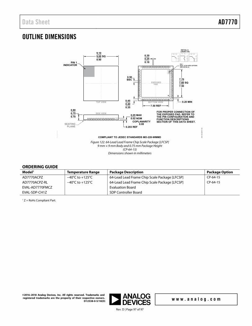
Data Sheet AD7770
Rev. D | Page 97 of 97
OUTLINE DIMENSIONS
0.50BSC
BOTTOM VIEWTOP VIEW
PIN 1INDICATOR
7.707.60 SQ7.50
0.450.400.35
0.800.750.70
0.05 MAX0.02 NOM
0.203 REF
COPLANARITY0.08
0.300.250.18
04-
10
-20
17-
A
9.109.00 SQ8.90
FOR PROPER CONNECTION OFTHE EXPOSED PAD, REFER TOTHE PIN CONFIGURATION ANDFUNCTION DESCRIPTIONSSECTION OF THIS DATA SHEET.
0.20 MIN
7.50 REF
COMPLIANT TO JEDEC STANDARDS MO-220-WMMD
164
16
17
49
48
32
33
PK
G-0
04
39
6
SIDE VIEW
EXPOSEDPAD
PIN 1INDIC ATOR AREA OPTIONS(SEE DETAIL A)
DETAIL A(JEDEC 95)
SEATINGPLANE
Figure 122. 64-Lead Lead Frame Chip Scale Package [LFCSP]
9 mm × 9 mm Body and 0.75 mm Package Height (CP-64-15)
Dimensions shown in millimeters
ORDERING GUIDE Model1 Temperature Range Package Description Package Option AD7770ACPZ −40°C to +125°C 64-Lead Lead Frame Chip Scale Package [LFCSP] CP-64-15 AD7770ACPZ-RL −40°C to +125°C 64-Lead Lead Frame Chip Scale Package [LFCSP] CP-64-15 EVAL-AD7770FMCZ Evaluation Board
EVAL-SDP-CH1Z SDP Controller Board 1 Z = RoHs Compliant Part.
©2016–2018 Analog Devices, Inc. All rights reserved. Trademarks and registered trademarks are the property of their respective owners. D12538-0-5/18(D)