7 more op amps - University of California,...
24
EECS140 ANALOG CIRCUIT DESIGN MORE ON OP AMPS TELESCOPIC AND FOLDED CASCODE ROBERT W. BRODERSEN LECTURE 22 University of California Berkeley College of Engineering Department of Electrical Engineering and Computer Science Robert W. Brodersen EECS140 Fall,2002 Analog Circuit Design More on Op Amps TELESCOPIC and FOLDED CASCODE
Transcript of 7 more op amps - University of California,...
EECS140 ANALOG CIRCUIT DESIGN MORE ON OP AMPS TELESCOPIC AND FOLDED CASCODE
ROBERT W. BRODERSEN LECTURE 22
University of CaliforniaBerkeley
College of EngineeringDepartment of Electrical Engineering
and Computer Science
Robert W. BrodersenEECS140 Fall,2002
Analog Circuit Design
Moreon Op Amps
TELESCOPIC and FOLDED CASCODE
EECS140 ANALOG CIRCUIT DESIGN MORE ON OP AMPS TELESCOPIC AND FOLDED CASCODE
ROBERT W. BRODERSEN LECTURE 22
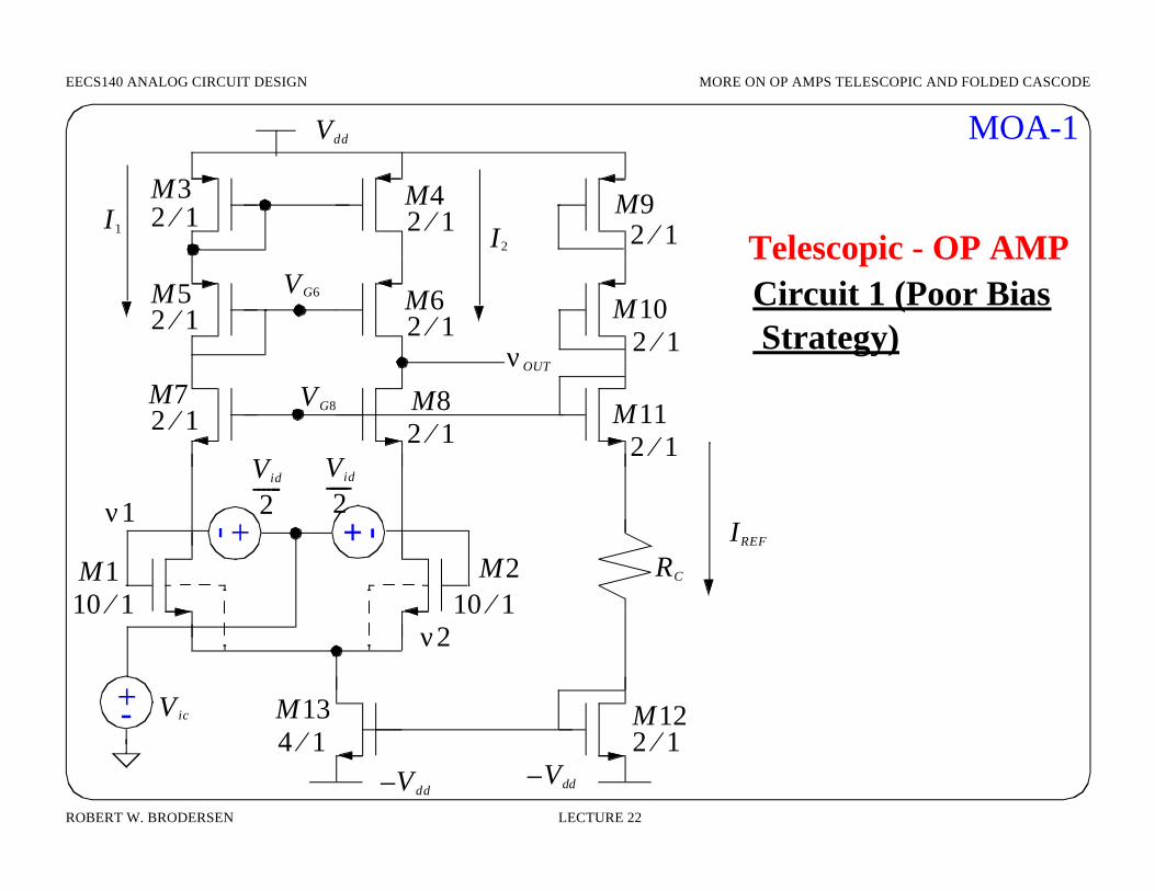
MOA-1
+ -+-
+-
Vdd
Vdd–V dd–
M13 M12
M11
M10
M9
M8M7
M6M5
M4M3
M2M1
V id
2------
V id
2------
IREF
I2
I1
RC
V ic
VG8
VG6
νOUT
Telescopic - OP AMPCircuit 1 (Poor Bias
4 1⁄
10 1⁄ν2
ν1
10 1⁄
2 1⁄
2 1⁄
2 1⁄
2 1⁄
2 1⁄
2 1⁄
2 1⁄
2 1⁄
2 1⁄
2 1⁄
Strategy)
EECS140 ANALOG CIRCUIT DESIGN MORE ON OP AMPS TELESCOPIC AND FOLDED CASCODE
ROBERT W. BRODERSEN LECTURE 22
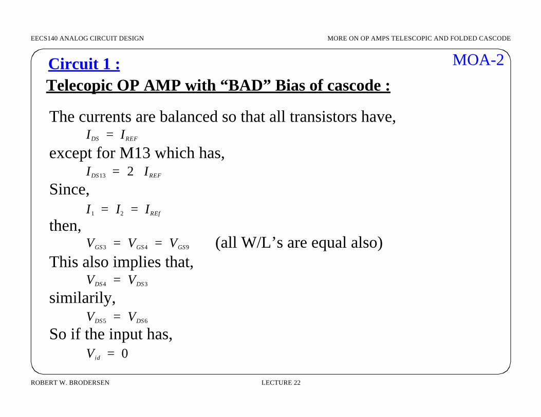
MOA-2Circuit 1 :Telecopic OP AMP with “BAD” Bias of cascode :
The currents are balanced so that all transistors have,IDS IREF=
except for M13 which has,
Since,IDS13 2 IREF⋅=
then,
This also implies that,
similarily,
So if the input has,
I1 I2 IREf= =
VGS3 VGS4 VGS9= =
VDS4 VDS3=
VDS5 VDS6=
V id 0=
(all W/L’s are equal also)
EECS140 ANALOG CIRCUIT DESIGN MORE ON OP AMPS TELESCOPIC AND FOLDED CASCODE
ROBERT W. BRODERSEN LECTURE 22
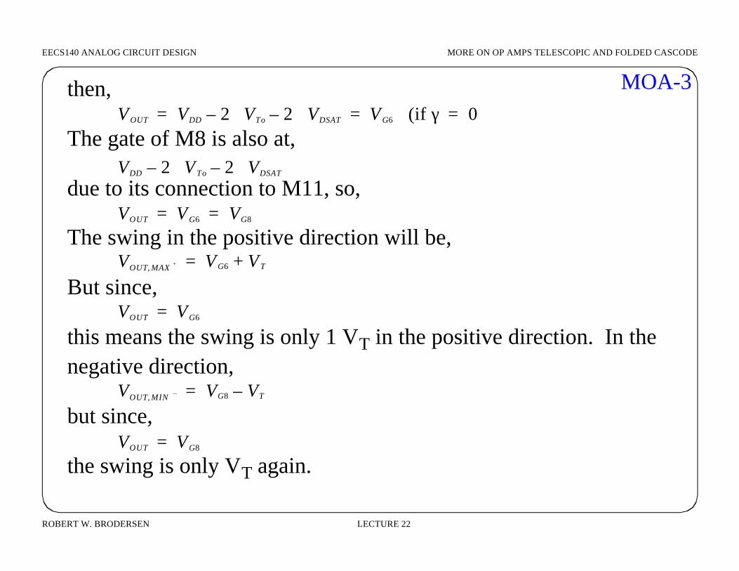
MOA-3then,
The gate of M8 is also at,
due to its connection to M11, so,
The swing in the positive direction will be,
But since,
this means the swing is only 1 VT in the positive direction. In the negative direction,
but since,
the swing is only VT again.
VOUT VDD 2 VTo 2 VDSAT⋅–⋅– VG6 (if γ 0 )= = =
VDD 2 V To 2 VDSAT⋅–⋅–
VOUT VG6 VG8= =
VOUT MAX +, VG6 V T+=
VOUT VG6=
VOUT MIN --, VG8 VT–=
VOUT VG8=
EECS140 ANALOG CIRCUIT DESIGN MORE ON OP AMPS TELESCOPIC AND FOLDED CASCODE
ROBERT W. BRODERSEN LECTURE 22
MOA-4
Thus the total swing is only 2VT ... not too good.In the positive direction we could use a high swing configurationas was described for the cascoded current source.On the low side we can use a better circuit.
Circuit 2 :
Telescopic with a cascode bias that gives a better swing in the negative direction.Maximum voltage in the positive direction is given by M6 goinglinear when,
Negative swing is limited by M8 going linear,
Set VA so that M1 & M2 are at the edge of saturation
VOUT MAX + , VDD VGS3 VDSAT6––>
VOUT MIN, -- VA VT8–=
EECS140 ANALOG CIRCUIT DESIGN LECTURES ON MOS DEVICE MODELS
ROBERT W. BRODERSEN LECTURE 2 FALL,1998
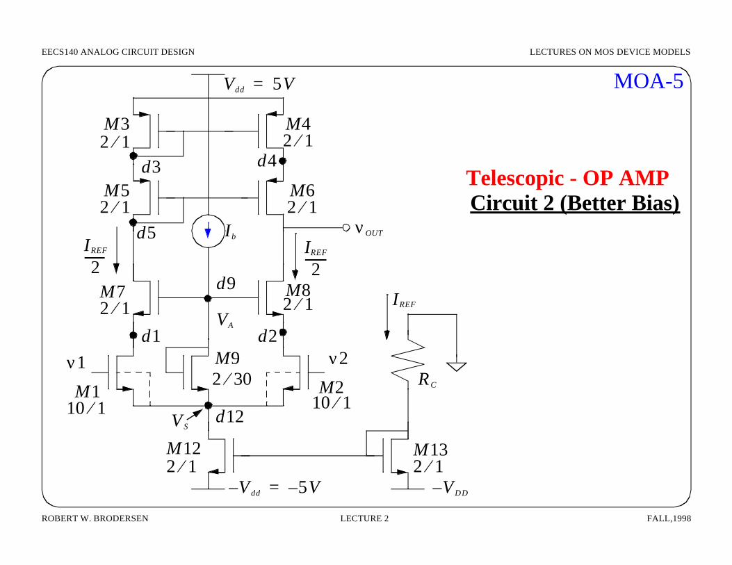
MOA-5
Circuit 2 (Better Bias)
M13M12
M9
M8M7
M6M5
M4M3
M2M1
IREF
2-------
Ib
RC
IREF
2-------
VA
V Sd12
d9
d5
d4d3
d2d1
νOUT
IREF
Telescopic - OP AMP
2 1⁄ 2 1⁄
2 1⁄
2 1⁄
2 1⁄
2 1⁄
2 1⁄
2 1⁄
10 1⁄10 1⁄
2 30⁄ν1 ν2
VDD–V dd– 5V–=
Vdd 5V=
EECS140 ANALOG CIRCUIT DESIGN LECTURES ON MOS DEVICE MODELS
ROBERT W. BRODERSEN LECTURE 2 FALL,1998
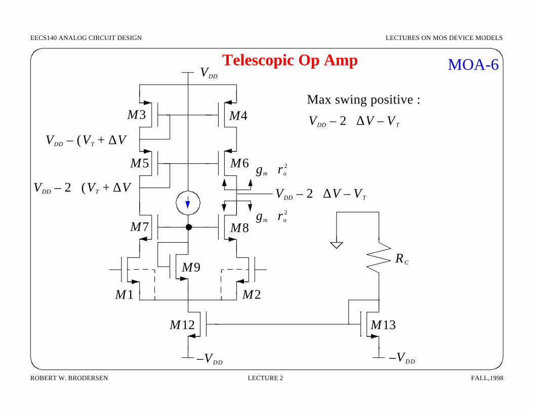
MOA-6Telescopic Op Amp
RC
M1 M2
M3 M4
M5 M6
M7 M8
M9
M12 M13
VDD
VDD– VDD–
VDD VT ∆V+( )–
VDD 2 VT ∆V+( )⋅– VDD 2 ∆V V T–⋅–
gm ro2⋅
gm ro2⋅
Max swing positive :
VDD 2 ∆V V T–⋅–
EECS140 ANALOG CIRCUIT DESIGN LECTURES ON MOS DEVICE MODELS
ROBERT W. BRODERSEN LECTURE 2 FALL,1998
Telescopic Op Amp (Cont.)
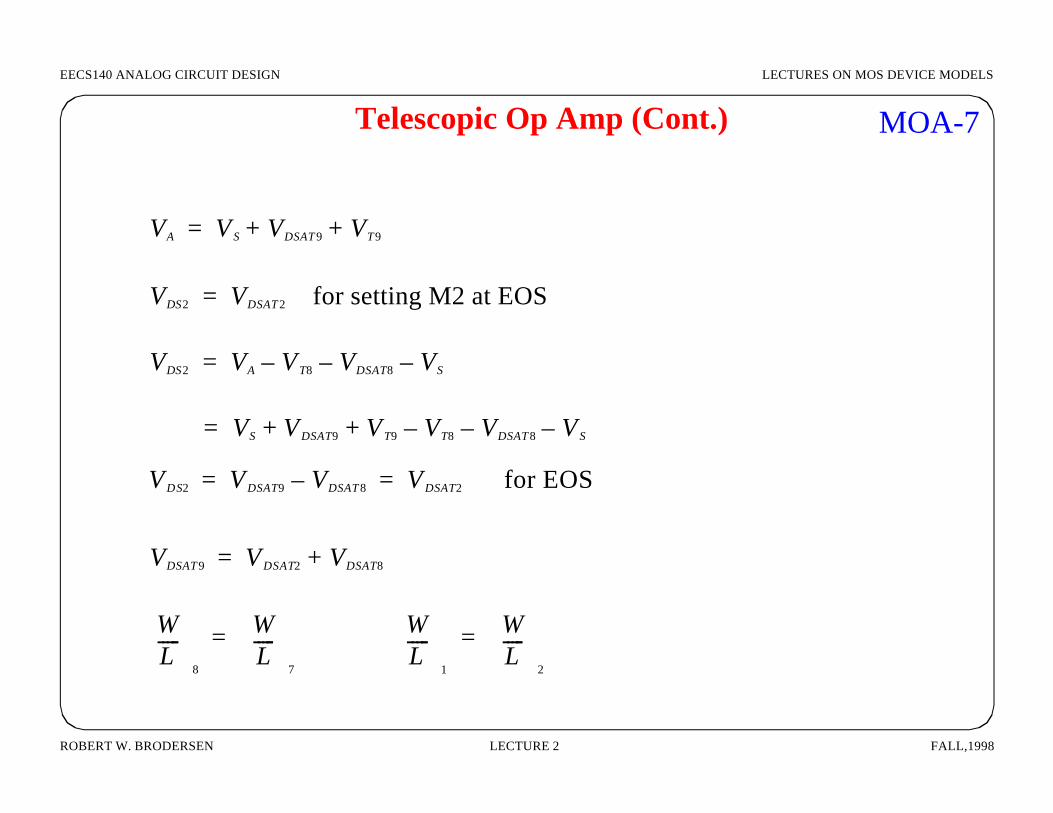
VA V S VDSAT 9 VT9+ +=
VDS2 VDSAT 2 for setting M2 at EOS=
VDS2 VA V T8 VDSAT8 VS–––=
VS VDSAT9 V T9 VT8 VDSAT 8 V S–––+ +=
VDS2 VDSAT9 VDSAT 8– VDSAT2 for EOS= =
VDSAT 9 VDSAT2 VDSAT8+=
WL-----
8
WL-----
7
= WL-----
1
WL-----
2
=
MOA-7
EECS140 ANALOG CIRCUIT DESIGN MORE ON OP AMPS TELESCOPIC AND FOLDED CASCODE
ROBERT W. BRODERSEN LECTURE 22
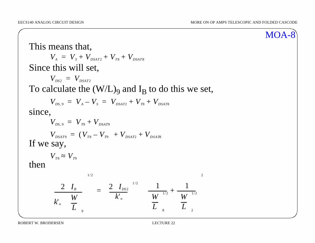
MOA-8This means that,
Since this will set,
To calculate the (W/L)9 and IB to do this we set,
since,
If we say,
then
VA V S VDSAT 2 VT8 VDSAT 8+ + +=
VDS2 VDSAT 2=
VDS 9, VA VS– VDSAT2 VT8 VDSAT8+ += =
VDS 9, V T9 VDSAT9+=
VDSAT 9 VT8 VT9–( ) VDSAT2 VDSAT8+ +=
VT8 VT9≈
2 IB⋅
k'nWL-----
9
⋅----------------------
1 2/
2 IDS2⋅k'n
--------------
1 2/ 1WL-----
8
1 2/---------------1
WL-----
2
1 2/---------------+
2
⋅=

EECS140 ANALOG CIRCUIT DESIGN MORE ON OP AMPS TELESCOPIC AND FOLDED CASCODE
ROBERT W. BRODERSEN LECTURE 22
MOA-9so,
if,
WL-----
9
IB
IS
---WL-----
8
1 2/–WL-----
2
1 2/–
+2
⋅=
WL-----
2
10=WL-----
8
2= IB 0.79µA= IS 10.5µA=
then,WL-----
9
115------≈
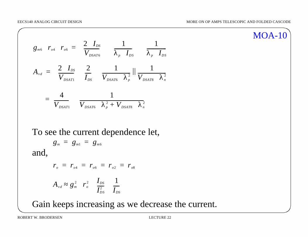
Gain and Rout
GM gm1 (cascoding has no effect on gm )=
ROUT gm6 r o4⋅( ) ro6⋅[ ] gm8 ro2⋅( ) ro8⋅[ ]||=
Aνd gm1gm6 gm8 r o4 r o6 ro2 ro8⋅ ⋅ ⋅( )⋅ ⋅gm6 ro4 ro6 gm8 ro2 ro8⋅ ⋅+⋅ ⋅
--------------------------------------------------------------⋅=
EECS140 ANALOG CIRCUIT DESIGN MORE ON OP AMPS TELESCOPIC AND FOLDED CASCODE
ROBERT W. BRODERSEN LECTURE 22
MOA-10
To see the current dependence let,
and,gm gm1 gm6= =
ro ro4 ro6 r o2 r o8= = = =
Aνd gm2 r o
2⋅ IDS
IDS2-----
1IDS
-----∼ ∼≈
Gain keeps increasing as we decrease the current.
gm6 ro4 ro6⋅ ⋅ 2 IDS⋅VDSAT 6
------------- 1
λp IDS⋅---------------
1λp IDS⋅---------------
⋅ ⋅=
Aνd2 IDS⋅VDSAT1
------------- 2
IDS
-----1
VDSAT6 λp2⋅
----------------------1
VDSAT8 λn2⋅
----------------------|| ⋅ ⋅=
4VDSAT1
------------1
VDSAT6 λp2 VDSAT8 λn
2⋅+⋅--------------------------------------------------
⋅=

EECS140 ANALOG CIRCUIT DESIGN LECTURES ON MOS DEVICE MODELS
ROBERT W. BRODERSEN LECTURE 2 FALL,1998
MOA-114.50
4.2504.0
3.7503.50
3.02.750
2.502.250
2.0
1.7501.50
1.2501.0
750.0M500.0M250.0M
0.-250.0M-500.0M
3.250
VOLTS
LIN
VOLTS [LIN]-20.0M -10.0M 0. 10.0M 20.0M
CASCODED DIFF PAIR - GATE VOLTAGE SWEEP96 / 10 / 05 14:40:14
DIFCAS2.SW0V(VOUT) ∆
Gain = 3.5k
Gain = 240k
EECS140 ANALOG CIRCUIT DESIGN LECTURES ON MOS DEVICE MODELS
ROBERT W. BRODERSEN LECTURE 2 FALL,1998
MOA-12
4.2504.0
3.7503.50
3.02.750
2.502.250
2.0
1.7501.50
1.2501.0
750.0M500.0M250.0M
0.-250.0M
3.250
-547.94U-400.0U -200.0U 0. 200.0U 400.0U
513.699U
VOLTS
LIN
VOLTS [LIN]
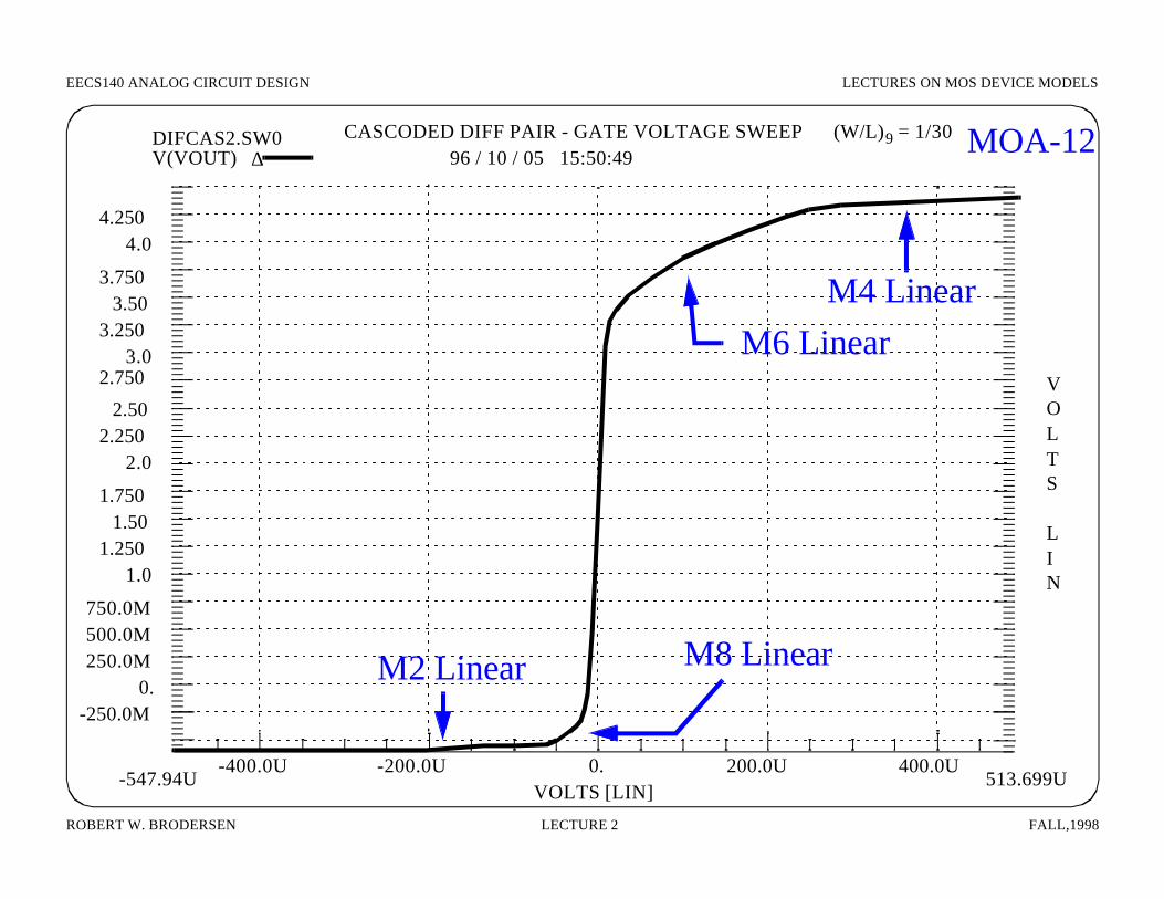
CASCODED DIFF PAIR - GATE VOLTAGE SWEEP96 / 10 / 05 15:50:49
DIFCAS2.SW0V(VOUT) ∆
(W/L)9 = 1/30
M6 Linear
M2 Linear M8 Linear
M4 Linear

EECS140 ANALOG CIRCUIT DESIGN LECTURES ON MOS DEVICE MODELS
ROBERT W. BRODERSEN LECTURE 2 FALL,1998
*****diff pair - gate voltage sw
eep
****** reading file: /bobtools/com
mercial/hspice/hspice.ini
*.model nch nm
os level = 1 tox = 170 vto = 0.7 kp = 90.0e-6 lambda = 0.01
+ gamm
a = 0.5 phi = 0.6 capop = 0 cgso=5.e-10 cgdo=5.e-10 cgbo=4.e-10 cj=1e-4
.model pch pm
os level = 1 tox = 170 vto = -0.7 kp = 30.0e-6 lambda =
0.01+ gam
ma = 0.5 phi = 0.6 capop = 0 cgso=3.e-11 cgdo=3.e-11 cgbo=4.e-10 cj=6e-4
.option nopage post=2 nomod
*name drain gate source bulk m
odelm
1 d1 vi1 vs vs nch l=1u w=10u
m2 d2 vi2 vs vs nch l=1u w
=10um
3 d3 d3 vdd vdd pch l=1u w=2u
m4 d4 d3 vdd vdd pch l=1u w
=2um
5 d5 d5 d3 vdd pch l=1u w=2u
m6 vout d5 d4 vdd pch l=1u w
=2um
7 d5 d9 d1 vdd- nch l=1u w=2u
m8 vout d9 d2 vdd- nch l=30u w
=2um
12 d12 d12 vdd- vdd- nch l=1u w=2u
m13 vs d12 vdd- vdd- nch l=1u w
=2u
rref 0 d12 180kr9 d9 vdd 5x
vic vic 0 0vid1 vi1 vic 0.0evid2 vic vi2 vi1 vic 1 *other half of the vid inputvdd vdd 0 5.0vdd- vdd- 0 -5.0 .dc vid1 -.02 .02 .00001 *sw
eep the input voltage*.dc vid1 -5 5 .1 *sw
eep the input voltage*.print dc v(out)*.print dc i(m
1) * i is the ids of m1
* * von=1v9 vdsat=1x9 gds=1x8*.print dc 1v9(m
1) 1v10(m1) 1x7(m
1) * plots gm=1x7 gm
bs=1x9 gds=1x8.op *initial operating point.tf v(vout,0) vid1 *.m
easure tot_power avg pow
er *makes it do the pow
er calculation
.end
MOA-13
EECS140 ANALOG CIRCUIT DESIGN MORE ON OP AMPS TELESCOPIC AND FOLDED CASCODE
ROBERT W. BRODERSEN LECTURE 22
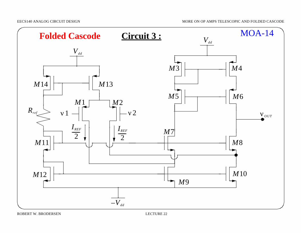
MOA-14
V dd
V dd–
M13
M12
M11
M10M9
M4M3
M6M5
M14
M2M1Rref νOUT
Vdd
M8M7IREF
2-------
ν1 ν2
IREF
2-------
Folded Cascode Circuit 3 :

EECS140 ANALOG CIRCUIT DESIGN LECTURES ON FREQUENCY RESPONSE
ROBERT W. BRODERSEN LECTURE 22 FALL,1998
MOA-15
4.50
4.03.50
3.0
2.502.0
1.501.0
500.0M0.
-500.0M
-1.0-1.50
-2.0-2.50
-3.0
-3.50-4.0
-4.50-5.0
-3.0M -2.0M -1.0M 0. 1.0M 2.0M 3.0M
VOLTS
LIN
VOLTS [LIN]
FOLDED CASCODE - VID AND VIC SWEEPS96 / 10 / 05 17:37:00
FOLD.SW0V(VOUT) ∆
EECS140 ANALOG CIRCUIT DESIGN LECTURES ON FREQUENCY RESPONSE
ROBERT W. BRODERSEN LECTURE 22 FALL,1998
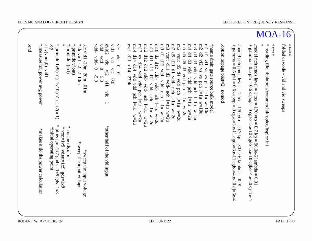
MOA-16*****folded cascode - vid and vic sw
eeps
****** reading file: /bobtools/com
mercial/hspice/hspice.ini
*.model nch nm
os level = 1 tox = 170 vto = 0.7 kp = 90.0e-6 lambda = 0.01
+ gamm
a = 0.5 phi = 0.6 capop = 0 cgso=5.e-10 cgdo=5.e-10 cgbo=4.e-10 cj=1e-4
.model pch pm
os level = 1 tox = 170 vto = -0.7 kp = 30.0e-6 lambda =
0.01+ gam
ma = 0.5 phi = 0.6 capop = 0 cgso=3.e-11 cgdo=3.e-11 cgbo=4.e-10 cj=6e-4
.option nopage post=2 nomod
*name drain gate source bulk m
odelm
1 d1 vi1 vs vs pch l=1u w=10u
m2 d2 vi2 vs vs pch l=1u w
=10um
3 d3 d3 vdd vdd pch l=1u w=2u
m4 d4 d3 vdd vdd pch l=1u w
=2um
5 d5 d5 d3 vdd pch l=1u w=2u
m6 vout d5 d4 vdd pch l=1u w
=2um
7 d5 d11 d1 vdd- nch l=1u w=2u
m8 vout d11 d2 vdd- nch l=1u w
=2um
9 d1 d12 vdd- vdd- nch l=1u w=2u
m10 d2 d12 vdd- vdd- nch l=1u w
=2um
11 d11 d11 d12 vdd- nch l=1u w=2u
m12 d12 d12 vdd- vdd- nch l=1u w
=2um
13 vs d14 vdd vdd pch l=1u w=2u
m14 d14 d14 vdd vdd pch l=1u w
=2urref d11 d14 270k
vic vic 0 0vid1 vi1 vic 0.0evid2 vic vi2 vi1 vic 1 *other half of the vid inputvdd vdd 0 5.0vdd- vdd- 0 -5.0 .dc vid1 -20m
20m .01m
*sweep the input voltage
*.dc vid1 -.2 .2 10m *sw
eep the input voltage*.print dc v(out)*.print dc i(m
1) * i is the ids of m1
* * von=1v9 vdsat=1x9 gds=1x8*.print dc 1v9(m
1) 1v10(m1) 1x7(m
1) * plots gm=1x7 gm
bs=1x9 gds=1x8.op *initial operating point.tf v(vout,0) vid1 *.m
easure tot_power avg pow
er *makes it do the pow
er calculation
.end
EECS140 ANALOG CIRCUIT DESIGN LECTURES ON FREQUENCY RESPONSE
ROBERT W. BRODERSEN LECTURE 22 FALL,1998
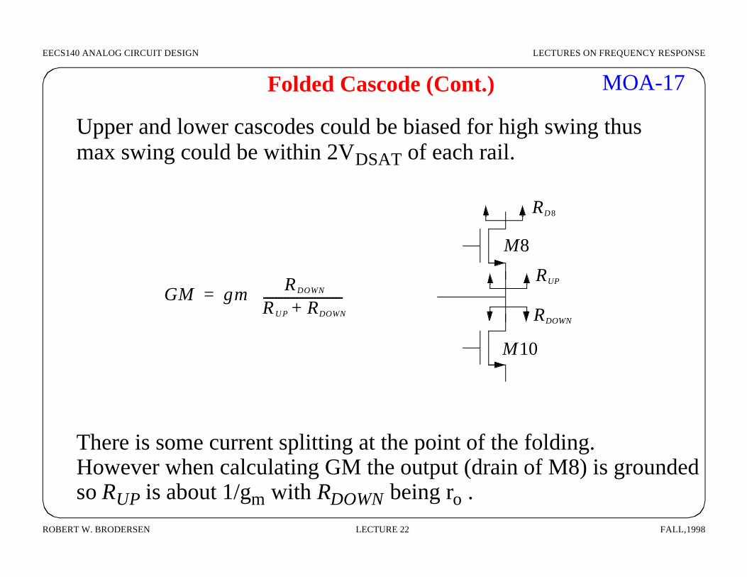
Folded Cascode (Cont.)
Upper and lower cascodes could be biased for high swing thusmax swing could be within 2VDSAT of each rail.
There is some current splitting at the point of the folding.However when calculating GM the output (drain of M8) is grounded so RUP is about 1/gm with RDOWN being ro .
RD8
RUP
RDOWN
M8
M10
GM gm RDOWN
RU P RDOWN+--------------------------⋅=
MOA-17
EECS140 ANALOG CIRCUIT DESIGN LECTURES ON FREQUENCY RESPONSE
ROBERT W. BRODERSEN LECTURE 22 FALL,1998
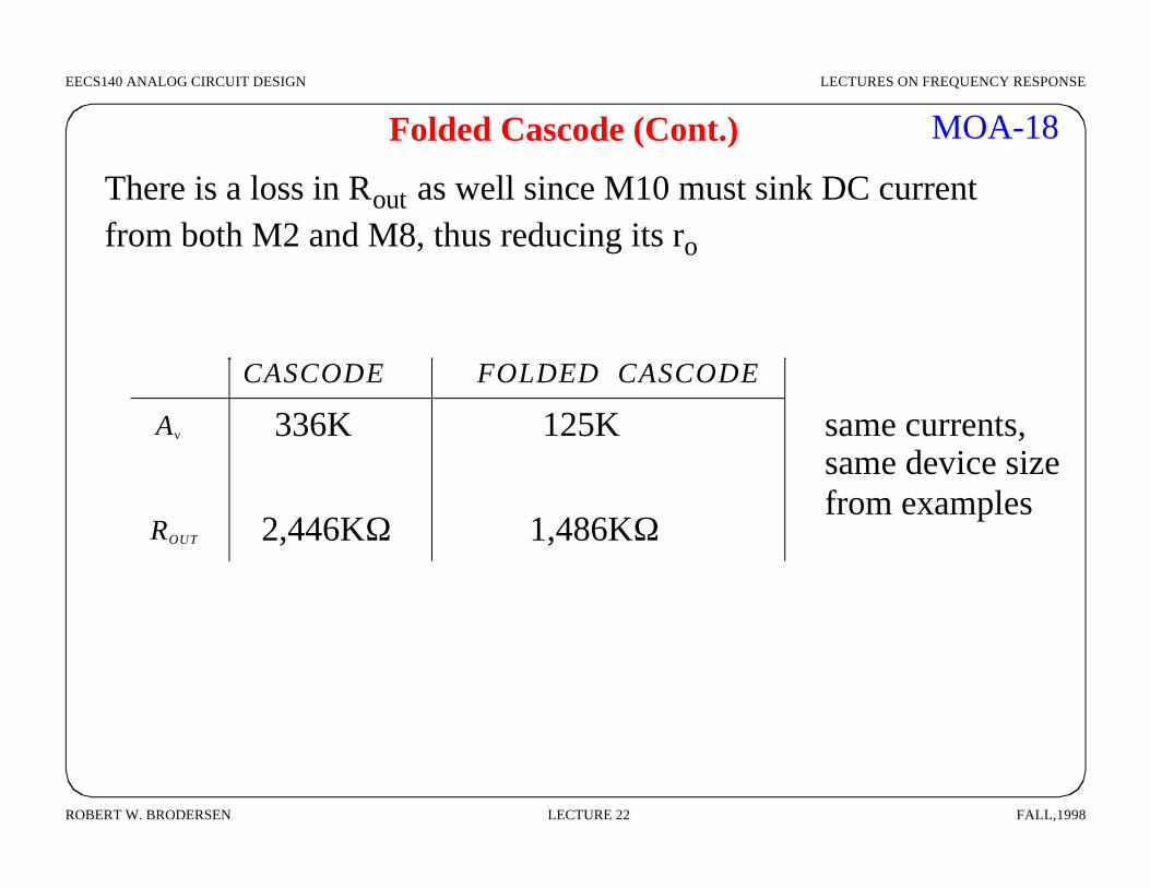
MOA-18Folded Cascode (Cont.)
There is a loss in Rout as well since M10 must sink DC currentfrom both M2 and M8, thus reducing its ro
Aν
ROUT
CASCODE FOLDED CASCODE
same currents,
from examplessame device size
336K 125K
2,446KΩ 1,486KΩ
EECS140 ANALOG CIRCUIT DESIGN LECTURES ON MOS DEVICE MODELS
ROBERT W. BRODERSEN LECTURE 2 FALL,1998
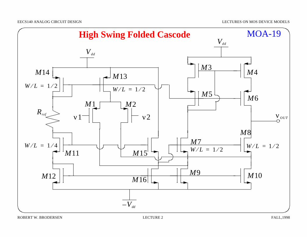
MOA-19
V dd
Vdd–
M13
M12
M11
M10M9
M4M3
M6M5
M14
M2M1Rref νOUT
Vdd
M16
M8M7
M15
High Swing Folded Cascode
ν1 ν2
W L⁄ 1 2⁄= W L⁄ 1 2⁄=
W L⁄ 1 2⁄= W L⁄ 1 2⁄=W L⁄ 1 4⁄=
EECS140 ANALOG CIRCUIT DESIGN MORE ON OP AMPS TELESCOPIC AND FOLDED CASCODE
ROBERT W. BRODERSEN LECTURE 22
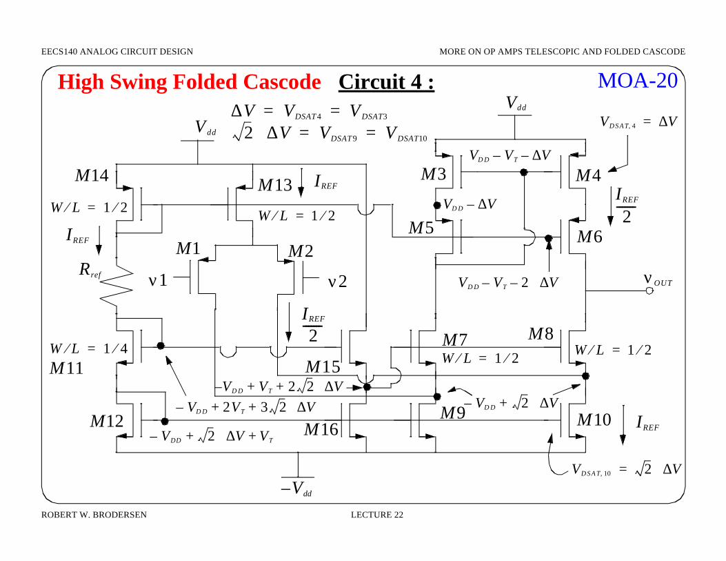
MOA-20
V dd
Vdd–
M13
M12
M11
M10M9
M4M3
M6M5
M14
M2M1Rref νOUT
Vdd
M16
M8M7M15
ν1 ν2
W L⁄ 1 2⁄= W L⁄ 1 2⁄=
W L⁄ 1 2⁄= W L⁄ 1 2⁄=W L⁄ 1 4⁄=
High Swing Folded Cascode Circuit 4 :∆V VDSAT 4 VDSAT3= =
2 ∆V⋅ VDSAT 9 VDSAT10= =
IREF
2-------
IREF
IREF
IREF
IREF
2-------
VD S A T 10, 2 V∆⋅=
VD D– 2 V∆⋅+V– D D VT 2 2 V∆⋅+ +
VDD– 2 V∆⋅ VT+ +
VD D– 2VT 3 2 V∆⋅+ +
VD S A T 4, V∆=
VD D VT– 2 V∆⋅–
VD D V∆–
VD D VT– V∆–

EECS140 ANALOG CIRCUIT DESIGN LECTURES ON MOS DEVICE MODELS
ROBERT W. BRODERSEN LECTURE 2 FALL,1998
MOA-21
VOLTS [LIN]-1.0M 1.0M 2.0M-2.0M 0.
HIGH SWING FOLDED CASCODE - VID AND VIC SWEEPS96 / 10 / 06 11:39:37
FOLD2.SW0V(VOUT) ∆ V(VOUT)
FOLD.SW0
High Swing Improvement
EECS140 ANALOG CIRCUIT DESIGN MORE ON OP AMPS TELESCOPIC AND FOLDED CASCODE
ROBERT W. BRODERSEN LECTURE 22
M15-M16 perform level shift to bias M9 and M10 at the edge
M7 and M8 have 1/2 sized W/L because the current is Iref/2.The connection to M5 from M14 sets the M3 at the
MOA-22
Circuit 4 :
of linear.
linear operation.The W/L’s are 1 unless otherwise shown. This is smaller than youwould want to use, but this was done to show the ratioing that isrequired to place the output in high swing.The Gain and Rout calculations are the same as for circuit 3 and arecarried out as described by DP-21 to DP-23.
edge of

EECS140 ANALOG CIRCUIT DESIGN LECTURES ON FREQUENCY RESPONSE
ROBERT W. BRODERSEN LECTURE 22 FALL,1998
MOA-23High Swing Folded Cascode (Cont.)
RO UP,
r o8 RD+1 1 χ+( ) r o8 gm8⋅ ⋅+------------------------------------------------=
RD 0→
RO UP,1
1r o8
----- 1 χ+( ) gm8⋅+----------------------------------------
11 χ+( ) gm8⋅
----------------------------≈=
RD gm ro2⋅≈ χ 0=
RO UP,
r o8 gm6 r o4 ro6⋅ ⋅+1 1 χ+( ) r o8 gm8⋅ ⋅+------------------------------------------------=
RO UP,gm6 ro4 ro6⋅ ⋅
r o8 gm8⋅-------------------------- r o≈ ≈
ROUT S8,ro
3---≈