
56F8014 Technical Data - Data Sheet
125
56F8000 16-bit Digital Signal Controllers freescale.com 56F8014 Data Sheet Technical Data MC56F8014 Rev. 11 05/2008
Transcript of 56F8014 Technical Data - Data Sheet
56F800016-bit Digital Signal Controllers
freescale.com
56F8014Data SheetTechnical Data
MC56F8014Rev. 1105/2008

56F8014 Technical Data, Rev. 11
2 Freescale Semiconductor
Document Revision History
Version History Description of Change
Rev 0 Initial release
Rev 1 Updates to Part 10, Specifications, Table 10-1, added maximum clamp current, per pinTable 10-11, clarified variation over temperature table and graphTable 10-15, added LIN slave timing
Rev 2 Added alternate pins to Figure 11-1 and Table 11-1.
Rev 3 Corrected bit selects in Timer Channel 3 Input (TC3_INP) bit 9, Section 6.3.1.7, clarified Section 1.4.1, and simplified notes in Table 10-9,
Rev 4 Added clarification on sync inputs in Section 1.4.1, added voltage difference specification to Table 10-1 and Table 10-4, deleted formula for Ambient Operating Temperature in Table 10-4, and a note for pin group 3, corrected Table 8-1, error in Port C peripheral function configuration, updated notes in Table 10-9. Added RoHs and “pb-free” language to back cover.
Rev 5 Updates to Section 10Table 10-5, corrected max values for ADC Input Current High and Low; corrected typ value for pull-up disabled Digital Input Current Low (a)Table 10-6, corrected typ and added max values for Standby > Stop and Powerdown modesTable 10-7, corrected min value for Low-Voltage Interrupt for 3.3VTable 10-11, corrected typ and max values and units for PLL lock timeTable 10-12, corrected typ values for Relaxation Oscillator output frequency and variation over temperature (also increased temp range to 150 degreesC) and added variation over temperature from 0—105 degreesCUpdated Figure 10-5Table 10-19, updated max values for Integral Non-Linearity full input signal range, Negative Differential Non-Linearity, ADC internal clock, Offset Voltage Internal Ref, Gain Error and Offset Voltage External Ref; updated typ values for Negative Differential Non-Linearity, Offset Voltage Internal Ref, Gain Error and Offset Voltage External Ref; added new min values and corrected typ values for Signal-to-noise ratio, Total Harmonic Distortion, Spurious Free Dynamic Range, Signal-to-noise plus distortion, Effective Number of Bits
Rev 6 Added details to Section 1. Clarified language in State During Reset column in Table 2-3; corrected flash data retention temperature in Table 10-4; moved input current high/low toTable 10-19 and location of footnotes in Table 10-5; reorganized Table 10-19; clarified title of Figure 10-1.
Rev. 7 • In Table 10-4, added an entry for flash data retention with less than 100 program/erase cycles (minimum 20 years).
• In Table 10-6, changed the device clock speed in STOP mode from 8MHz to 4MHz.• In Table 10-12, changed the typical relaxation oscillator output frequency in Standby mode
from 400kHz to 200kHz.
Rev. 8 In Table 10-19, changed the maximum ADC internal clock frequency from 8MHz to 5.33MHz.

56F8014 Technical Data, Rev. 11
Freescale Semiconductor 3
Rev. 9 Added the following note to the description of the TMS signal in Table 2-3:Note: Always tie the TMS pin to VDD through a 2.2K resistor.
Rev. 10 • In Table 2-3, changed VCAP value from 4.7 μF to 2.2 μF.
• In Table 2-3, changed the input type for FAULT3 (was “Output”, is “Input”).• In Table 2-3, changed the input type for FAULT2 (was “Input/Output”, is “Input”).• Revised Section 7, Security Features.• Added MC56F8014MFAE to Section 13, Ordering Information.• Fixed miscellaneous errors.
Rev.11 • Updated temperature information in Table 10-1 and Table 10-4.
Document Revision History (Continued)
Version History Description of Change
Please see http://www.freescale.com for the most current data sheet revision.

56F8014 Technical Data, Rev. 11
4 Freescale Semiconductor
56F8014 Block Diagram
Program Controllerand Hardware Looping Unit
Data ALU16 x 16 + 36 -> 36-Bit MAC
Three 16-bit Input RegistersFour 36-bit Accumulators
Address Generation Unit
Bit Manipulation
Unit
16-Bit56800E Core
InterruptController
4
Unified Data / Program RAM
4KB
PDB
PDB
XAB1XAB2
XDB2
CDBR
SPI or I2C or Timer
or GPIOB
IPBus Bridge (IPBB)
System BusControl
R/W ControlMemory
PAB
PAB
CDBW
CDBRCDBW
JTAG/EOnCE Port or GPIOD
Digital Reg Analog Reg
Low-VoltageSupervisor
VCAP VDD VSS_IO VDDA VSSA4
RESET
5
Timer or GPIOB
AD0
2
4
ClockGenerator*
SystemIntegration
Module
POR
OSC
PWM Outputs
PWMor Timer Port
or GPIOA
*Includes On-Chip Relaxation Oscillator
COP/Watchdog
AD14Program Memory
8K x 16 Flash
ADCor
GPIOC
SCI or I2C
or GPIOB
2
2
• Up to 32 MIPS at 32MHz core frequency• DSP and MCU functionality in a unified,
C-efficient architecture• 16KB Program Flash • 4KB Unified Data/Program RAM• One 5-channel PWM module• Two 4-channel 12-bit ADCs• One Serial Communication Interface (SCI) with LIN
slave functionality• One Serial Peripheral Interface (SPI)• One 16-bit Quad Timer
• One Inter-Integrated Circuit (I2C) Port• Computer Operating Properly (COP)/Watchdog• On-Chip Relaxation Oscillator• Integrated Power-On Reset and Low-Voltage Interrupt
Module• JTAG/Enhanced On-Chip Emulation (OnCE™) for
unobtrusive, real-time debugging• Up to 26 GPIO lines• 32-pin LQFP Package
56F8014 General Description

56F8014 Technical Data, Rev. 11
Freescale Semiconductor 5
Part 1: Overview . . . . . . . . . . . . . . . . . . . . . . . 61.1. 56F8014 Features . . . . . . . . . . . . . . . . . . . . 61.2. 56F8014 Description. . . . . . . . . . . . . . . . . . . 81.3. Award-Winning Development Environment . 81.4. Architecture Block Diagram . . . . . . . . . . . . . 91.5. Synchronize ADC with PWM . . . . . . . . . . . . 91.6. Multiple Frequency PWM Output . . . . . . . . . 91.7. Product Documentation . . . . . . . . . . . . . . . 131.8. Data Sheet Conventions. . . . . . . . . . . . . . . 13
Part 2: Signal/Connection Descriptions . . . 142.1. Introduction. . . . . . . . . . . . . . . . . . . . . . . . . 142.2. 56F8014 Signal Pins . . . . . . . . . . . . . . . . . 18
Part 3: OCCS . . . . . . . . . . . . . . . . . . . . . . . . . 263.1. Overview. . . . . . . . . . . . . . . . . . . . . . . . . . . 263.2. Features . . . . . . . . . . . . . . . . . . . . . . . . . . . 263.3. Operating Modes . . . . . . . . . . . . . . . . . . . . 263.4. Block Diagram . . . . . . . . . . . . . . . . . . . . . . 283.5. Pin Descriptions . . . . . . . . . . . . . . . . . . . . . 29
Part 4: Memory Map . . . . . . . . . . . . . . . . . . . 294.1. Introduction. . . . . . . . . . . . . . . . . . . . . . . . . 294.2. Interrupt Vector Table . . . . . . . . . . . . . . . . . 294.3. Program Map . . . . . . . . . . . . . . . . . . . . . . . 314.4. Data Map . . . . . . . . . . . . . . . . . . . . . . . . . . 324.5. EOnCE Memory Map . . . . . . . . . . . . . . . . . 324.6. Peripheral Memory Mapped Registers . . . . 33
Part 5: Interrupt Controller (ITCN) . . . . . . . . 435.1. Introduction. . . . . . . . . . . . . . . . . . . . . . . . . 435.2. Features . . . . . . . . . . . . . . . . . . . . . . . . . . . 435.3. Functional Description . . . . . . . . . . . . . . . . 435.4. Block Diagram . . . . . . . . . . . . . . . . . . . . . . 455.5. Register Descriptions . . . . . . . . . . . . . . . . . 455.6. Resets . . . . . . . . . . . . . . . . . . . . . . . . . . . . 61
Part 6: System Integration Module (SIM) . . 626.1. Introduction. . . . . . . . . . . . . . . . . . . . . . . . . 626.2. Features . . . . . . . . . . . . . . . . . . . . . . . . . . . 626.3. Register Descriptions . . . . . . . . . . . . . . . . . 646.4. Clock Generation Overview . . . . . . . . . . . . 776.5. Power-Down Modes . . . . . . . . . . . . . . . . . . 776.6. Resets . . . . . . . . . . . . . . . . . . . . . . . . . . . . 796.7. Clocks. . . . . . . . . . . . . . . . . . . . . . . . . . . . . 816.8. Interrupts . . . . . . . . . . . . . . . . . . . . . . . . . . 82
Part 7: Security Features . . . . . . . . . . . . . . .827.1. Operation with Security Enabled . . . . . . . . . 827.2. Flash Access Lock and Unlock Mechanisms 837.3. Product Analysis. . . . . . . . . . . . . . . . . . . . . . 84
Part 8: General Purpose Input/Output (GPIO). . . . . . . . . . . . . . . . . . . . . . . . . . . . . . .84
8.1. Introduction. . . . . . . . . . . . . . . . . . . . . . . . . . 848.2. Configuration . . . . . . . . . . . . . . . . . . . . . . . . 848.3. Reset Values . . . . . . . . . . . . . . . . . . . . . . . . 86
Part 9: Joint Test Action Group (JTAG) . . .919.1. 56F8014 Information . . . . . . . . . . . . . . . . . . 91
Part 10: Specifications . . . . . . . . . . . . . . . . .9110.1. General Characteristics . . . . . . . . . . . . . . . 9110.2. DC Electrical Characteristics . . . . . . . . . . . 9510.3. AC Electrical Characteristics . . . . . . . . . . . 9710.4. Flash Memory Characteristics . . . . . . . . . . 9810.5. External Clock Operation Timing . . . . . . . . 9910.6. Phase Locked Loop Timing . . . . . . . . . . . . 9910.7. Relaxation Oscillator Timing. . . . . . . . . . . 10010.8. Reset, Stop, Wait, Mode Select, and
Interrupt Timing . . . . . . . . . . . . . . 10110.9. Serial Peripheral Interface (SPI) Timing . . 10210.10. Quad Timer Timing. . . . . . . . . . . . . . . . . 10510.11. Serial Communication Interface (SCI)
Timing . . . . . . . . . . . . . . . . . . . . . 10710.12. Inter-Integrated Circuit Interface (I2C)
Timing . . . . . . . . . . . . . . . . . . . . . 10810.13. JTAG Timing. . . . . . . . . . . . . . . . . . . . . . 10910.14. Analog-to-Digital Converter (ADC)
Parameters . . . . . . . . . . . . . . . . . 11110.15. Equivalent Circuit for ADC Inputs . . . . . . 11210.16. Power Consumption . . . . . . . . . . . . . . . . 112
Part 11: Packaging . . . . . . . . . . . . . . . . . . .11511.1. 56F8014 Package and Pin-Out
Information . . . . . . . . . . . . . . . . . . 115
Part 12: Design Considerations . . . . . . . . .11812.1. Thermal Design Considerations . . . . . . . . 11812.2. Electrical Design Considerations . . . . . . . 119
Part 13: Ordering Information . . . . . . . . . .121
Part 14: Appendix . . . . . . . . . . . . . . . . . . . .122
56F8014 Data Sheet Table of Contents

56F8014 Technical Data, Rev. 11
6 Freescale Semiconductor
Part 1 Overview
1.1 56F8014 Features
1.1.1 Digital Signal Controller Core• Efficient 16-bit 56800E family Digital Signal Controller (DSC) engine with dual Harvard architecture• As many as 32 Million Instructions Per Second (MIPS) at 32MHz core frequency• Single-cycle 16 × 16-bit parallel Multiplier-Accumulator (MAC)• Four 36-bit accumulators, including extension bits• 32-bit arithmetic and logic multi-bit shifter• Parallel instruction set with unique DSP addressing modes• Hardware DO and REP loops• Three internal address buses• Four internal data buses• Instruction set supports both DSP and controller functions• Controller-style addressing modes and instructions for compact code• Efficient C compiler and local variable support• Software subroutine and interrupt stack with depth limited only by memory• JTAG/Enhanced On-Chip Emulation (OnCE) for unobtrusive, processor speed-independent, real-time
debugging
1.1.2 Memory• Dual Harvard architecture permits as many as three simultaneous accesses to program and data memory• Flash security and protection that prevent unauthorized users from gaining access to the internal Flash• On-chip memory
— 16KB of Program Flash— 4KB of Unified Data/Program RAM
• EEPROM emulation capability using Flash
1.1.3 Peripheral Circuits for 56F8014• One multi-function five-output Pulse Width Modulator (PWM) module
— Up to 96MHz PWM operating clock— 15 bits of resolution— Center-aligned and Edge-aligned PWM signal mode— Three programmable fault inputs with programmable digital filter— Double-buffered PWM registers

56F8014 Features
56F8014 Technical Data, Rev. 11
Freescale Semiconductor 7
— Each complementary PWM signal pair can output a different switching frequency by selecting PWM generation sources from: – PWM generator– External GPIO– Internal timers– ADC conversion result of over/under limits:
When conversion result is greater than high limit, deactivate PWM signalWhen conversion result is less than low limit, activate PWM signal
• Two independent 12-bit Analog-to-Digital Converters (ADCs)— 2 x 4 channel inputs— Supports both simultaneous and sequential conversions— ADC conversions can be synchronized by both PWM and timer modules— Sampling rate up to 2.67MSPS— 8-word result buffer registers— ADC Smart Power Management (Auto-standby, auto-powerdown)
• One 16-bit multi-purpose Quad Timer module (TMR) — Up to 96MHz operating clock— Four independent 16-bit counter/timers with cascading capability— Each timer has capture and compare capability— Up to 12 operating modes
• One Serial Communication Interface (SCI) with LIN slave functionality— Full-duplex or single-wire operation— Two receiver wake-up methods:
– Idle line– Address mark
• One Serial Peripheral Interface (SPI)— Full-duplex operation— Master and slave modes— Programmable length transactions (two to sixteen bits)
• One Inter-Integrated Circuit (I2C) port— Operates up to 400 kbps— Supports both master and slave operation
• Computer Operating Properly (COP)/Watchdog timer capable of selecting different clock sources• Up to 26 General-Purpose I/O (GPIO) pins with 5V tolerance• Integrated Power-On Reset and Low-Voltage Interrupt Module• Phase Lock Loop (PLL) provides a high-speed clock to the core and peripherals• Clock Sources:
— On-chip relaxation oscillator

56F8014 Technical Data, Rev. 11
8 Freescale Semiconductor
— External clock source• On-chip regulators for digital and analog circuitry to lower cost and reduce noise• JTAG/EOnCE debug programming interface for real-time debugging
1.1.4 Energy Information• Fabricated in high-density CMOS with 5V-tolerant, TTL-compatible digital inputs• On-chip regulators for digital and analog circuitry to lower cost and reduce noise• Wait and Stop modes available• ADC smart power management• Each peripheral can be individually disabled to save power
1.2 56F8014 DescriptionThe 56F8014 is a member of the 56800E core-based family of Digital Signal Controllers (DSCs). Itcombines, on a single chip, the processing power of a DSP and the functionality of a microcontroller witha flexible set of peripherals to create an extremely cost-effective solution. Because of its low cost,configuration flexibility, and compact program code, the 56F8014 is well-suited for many applications.The 56F8014 includes many peripherals that are especially useful for industrial control, motion control,home appliances, general purpose inverters, smart sensors, fire and security systems, switched-modepower supplies, power management, and medical monitoring applications.
The 56800E core is based on a dual Harvard-style architecture consisting of three execution unitsoperating in parallel, allowing as many as six operations per instruction cycle. The MCU-styleprogramming model and optimized instruction set allow straightforward generation of efficient, compactDSP and control code. The instruction set is also highly efficient for C compilers to enable rapiddevelopment of optimized control applications.
The 56F8014 supports program execution from internal memories. Two data operands can be accessedfrom the on-chip data RAM per instruction cycle. The 56F8014 also offers up to 26 General PurposeInput/Output (GPIO) lines, depending on peripheral configuration.
The 56F8014 Digital Signal Controller includes 16KB of Program Flash and 4KB of UnifiedData/Program RAM. Program Flash memory can be independently bulk erased or erased in pages.Program Flash page erase size is 512 Bytes/256 Words.
A full set of programmable peripherals—PWM, ADCs, SCI, SPI, I2C, Quad Timer—support variousapplications. Each peripheral can be independently shut down to save power. Any pin in these peripheralscan also be used as a General Purpose Input/Outputs (GPIO).
1.3 Award-Winning Development EnvironmentProcessor ExpertTM (PE) provides a Rapid Application Design (RAD) tool that combines easy-to-usecomponent-based software application creation with an expert knowledge system.
The CodeWarrior Integrated Development Environment is a sophisticated tool for code navigation,compiling, and debugging. A complete set of evaluation modules (EVMs), demonstration board kit anddevelopment system cards will support concurrent engineering. Together, PE, CodeWarrior and EVMs

Architecture Block Diagram
56F8014 Technical Data, Rev. 11
Freescale Semiconductor 9
create a complete, scalable tools solution for easy, fast, and efficient development.
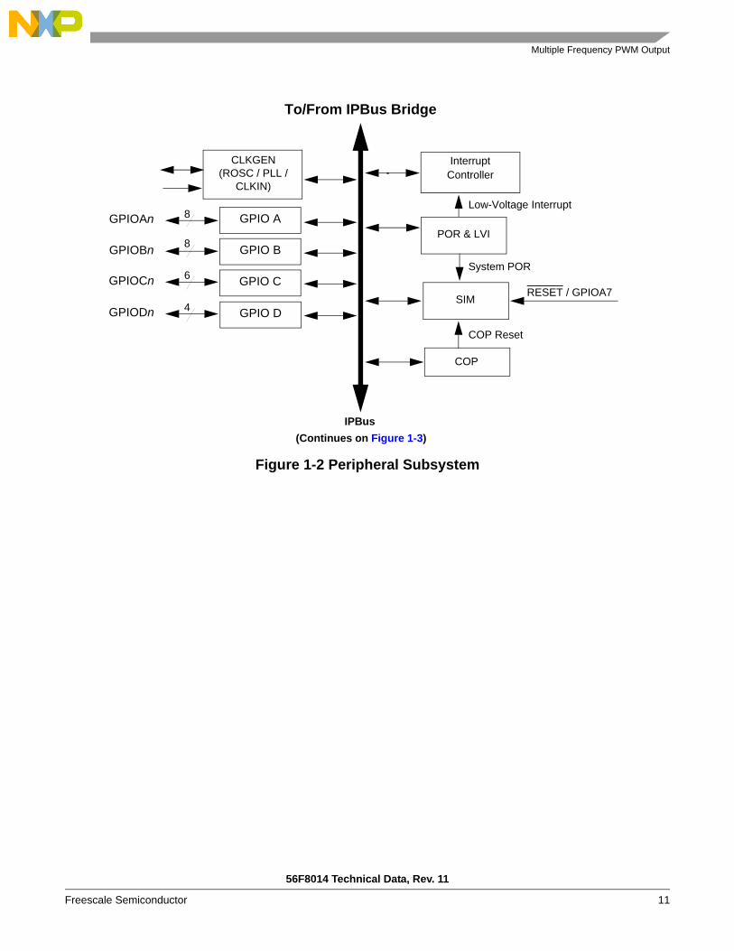
1.4 Architecture Block DiagramThe 56F8014’s architecture is shown in Figure 1-1, Figure 1-2, and Figure 1-3. Figure 1-1 illustrateshow the 56800E system buses communicate with internal memories and the IPBus Bridge, as well asshowing the internal connections between each unit of the 56800E core. Figure 1-2 shows the peripheralsand control blocks connected to the IPBus Bridge. Figure 1-3 details how the device’s I/O pins are muxed.The figures do not show the on-board regulator and power and ground signals. They also do not show themultiplexing between peripherals or the dedicated GPIOs. Please see Part 2 Signal/ConnectionDescriptions to see which signals are multiplexed with those of other peripherals.
1.5 Synchronize ADC with PWMADC conversion can be synchronized with the PWM module via Quad Timer channel 2 and 3 if needed.Internally, the PWM synch signal — which is generated at every PWM reload —can be connected to thetimer channel 3 input, and the timer channel 2 and channel 3 outputs are connected to the ADC sync inputs.Timer channel 3 output is connected to SYNC0 and timer channel 2 is connected to SYNC1. The settingis controlled by the TC3_INP bit in the SIM Control Register; see Section 6.3.1.
SYNC0 is the master ADC sync input, used to trigger both ADCA and ADCB in sequence and parallelmode. SYNC1 is used to trigger ADCB in parallel independent mode, while SYNC0 is used to triggerADCA. See MC56F8000RM, the 56F801X Peripheral Reference Manual, for additional information.
1.6 Multiple Frequency PWM OutputWhen both PWM channels of a complementary pair in software control mode and software control bitsare set to 1, each complementary PWM signal pair — PWM 0 and 1; PWM 2 and 3; and PWM 4 and 5 —can select a PWM source from one of the following sources. This will enable each PWM pair and PWM2to output PWM signals at different frequencies.
• External GPIO input:— GPIOB2 input can be used to drive PWM 0 and 1— GPIOB3 input can be used to drive PWM 2— GPIOB4 input can be used to drive PWM 4 and 5
• Quad Timer output:— Timer0 output can be used to drive PWM 0 and 1— Timer2 output can be used to drive PWM 2— Timer3 output can be used to drive PWM 4 and 5
• ADC conversion result:— Signal of over/under limit of ADC sample 0 can be used to drive PWM 0 and 1— Signal of over/under limit of ADC sample 1 can be used to drive PWM 2

56F8014 Technical Data, Rev. 11
10 Freescale Semiconductor
— Signal of over/under limit of ADC sample 2 can be used to drive PWM 4 and 5
Figure 1-1 56800E Core Block Diagram
Data
DSP56800E Core
ArithmeticLogic Unit
(ALU)
XAB2
PAB
PDB
CDBW
CDBR
XDB2
ProgramMemory
Data /
IPBUSInterface
Bit-Manipulation
Unit
N3M01
Address
XAB1
GenerationUnit
(AGU)
PCLA
LA2HWS0HWS1FIRA
OMRSR
FISR
LCLC2
InstructionDecoder
InterruptUnit
LoopingUnit
Program Control Unit ALU1 ALU2
MAC and ALU
A1A2 A0B1B2 B0C1C2 C0D1D2 D0Y1Y0X0
Enhanced
JTAG TAP
R2R3R4R5
SP
R0R1
N
Y
Multi-Bit Shifter
OnCE™
ProgramRAM
Multiple Frequency PWM Output
56F8014 Technical Data, Rev. 11
Freescale Semiconductor 11
Figure 1-2 Peripheral Subsystem
IPBus
GPIO A
Interrupt Controller
To/From IPBus Bridge
GPIO B
GPIO C
CLKGEN(ROSC / PLL /
CLKIN)
POR & LVI
SIMGPIO D
Low-Voltage Interrupt
System POR
COP Reset
RESET / GPIOA7
COP
GPIOAn
GPIOBn
GPIOCn
GPIODn
(Continues on Figure 1-3)
8
8
6
4

56F8014 Technical Data, Rev. 11
12 Freescale Semiconductor
Figure 1-3 56F8014 Peripheral I/O Pin-Out
To/From IPBus Bridge
3 to PWM
Sync0, Sync1
Over/Under Limits
ADC
ANA0, 1, 3
ANA2
VREFH, VREFL
ANB2
ANB0, 1, 3
IPBus
3
2 VREFH, VREFL
ANA2
ANB2
ANA0, 1, 33
SPI
I2C
SCI
2
T2o, T3o
T3i T2/3
T1
T0
Timer
PWM
PWM0 - 3
Fault3Fault0
Fault1, 2
PWM4, 5PWM4, 5
PWM0 - 3
Fault1, 2
Fault0
Fault3
T2, 3
2
3
from ADC
I2C is muxed with both SPI and SCI.T2 and T3 are muxed with SPI and PWM.
T1
T0
CLKO
TXD, RXD 2
2
2
2 T2, 3
ANB0, 1, 3
GPIOA0 - 3
GPIOA4 - 5
GPIOA6
GPIOB5
GPIOB4
GPIOB6 - 7
GPIOB0 - 1
GPIOB2 - 3
GPIOC0, 1, 3
GPIOC2, 6
GPIOC4, 5, 7
SDA, SCL
SCLK, SS
MISO, MOSI
4
2
2
Output Controls
2 2
2
(Continued from Figure 1-2)
Reload Pulse
Product Documentation
56F8014 Technical Data, Rev. 11
Freescale Semiconductor 13
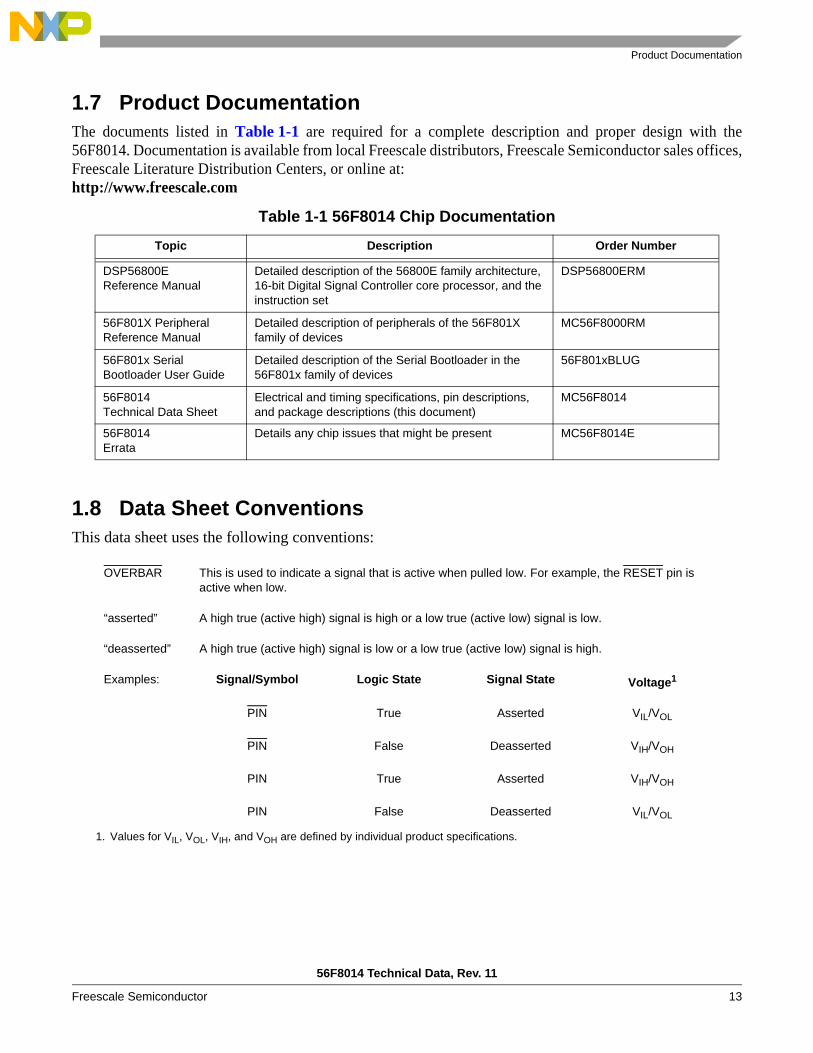
1.7 Product DocumentationThe documents listed in Table 1-1 are required for a complete description and proper design with the56F8014. Documentation is available from local Freescale distributors, Freescale Semiconductor sales offices,Freescale Literature Distribution Centers, or online at:http://www.freescale.com
Table 1-1 56F8014 Chip Documentation
1.8 Data Sheet ConventionsThis data sheet uses the following conventions:
Topic Description Order Number
DSP56800EReference Manual
Detailed description of the 56800E family architecture, 16-bit Digital Signal Controller core processor, and the instruction set
DSP56800ERM
56F801X Peripheral Reference Manual
Detailed description of peripherals of the 56F801X family of devices
MC56F8000RM
56F801x Serial Bootloader User Guide
Detailed description of the Serial Bootloader in the 56F801x family of devices
56F801xBLUG
56F8014Technical Data Sheet
Electrical and timing specifications, pin descriptions, and package descriptions (this document)
MC56F8014
56F8014Errata
Details any chip issues that might be present MC56F8014E
OVERBAR This is used to indicate a signal that is active when pulled low. For example, the RESET pin is active when low.
“asserted” A high true (active high) signal is high or a low true (active low) signal is low.
“deasserted” A high true (active high) signal is low or a low true (active low) signal is high.
Examples: Signal/Symbol Logic State Signal State Voltage1
1. Values for VIL, VOL, VIH, and VOH are defined by individual product specifications.
PIN True Asserted VIL/VOL
PIN False Deasserted VIH/VOH
PIN True Asserted VIH/VOH
PIN False Deasserted VIL/VOL

56F8014 Technical Data, Rev. 11
14 Freescale Semiconductor
Part 2 Signal/Connection Descriptions
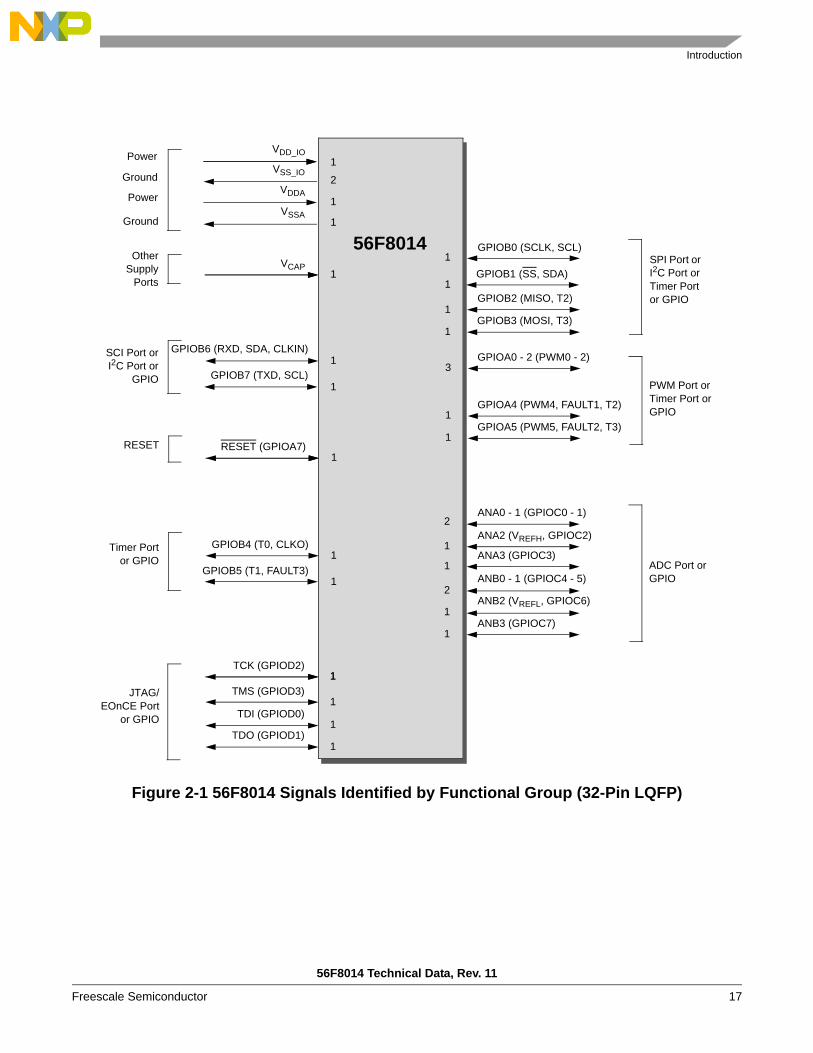
2.1 IntroductionThe input and output signals of the 56F8014 are organized into functional groups, as detailed in Table 2-1. Table 2-2 summarizes all device pins. In Table 2-2, each table row describes the signal or signals present on a pin, sorted by pin number.
Table 2-1 Functional Group Pin Allocations
Functional Group Number of Pins
Power (VDD or VDDA) 2
Ground (VSS or VSSA) 3
Supply Capacitors 1
Reset 1
Pulse Width Modulator (PWM) Ports1
1. Pins in this section can function as TMR and GPIO.
5
Serial Peripheral Interface (SPI) Ports2
2. Pins in this section can function as TMR, I2C, and GPIO.
4
Analog-to-Digital Converter (ADC) Ports 8
Timer Module Ports3
3. Pins can function as PWM and GPIO.
2
Serial Communications Interface (SCI) Ports4
4. Pins in this section can function as I2C and GPIO.
2
JTAG/Enhanced On-Chip Emulation (EOnCE) 4

Introduction
56F8014 Technical Data, Rev. 11
Freescale Semiconductor 15
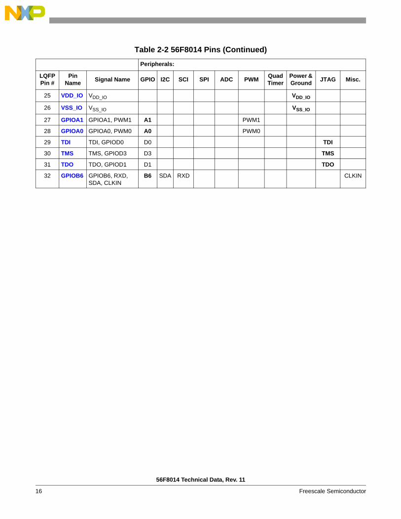
Table 2-2 56F8014 Pins
Peripherals:
LQFP Pin #
Pin Name Signal Name GPIO I2C SCI SPI ADC PWM Quad
TimerPower & Ground JTAG Misc.
1 GPIOB1 GPIOB1, SS, SDA
B1 SDA SS
2 GPIOB7 GPIOB7, TXD, SCL
B7 SCL TXD
3 GPIOB5 GPIOB5, T1, FAULT3
B5 FAULT3 T1
4 ANB0 ANB0, GPIOC4 C4 ANB0
5 ANB1 ANB1, GPIOC5 C5 ANB1
6 ANB2 ANB2, VREFL, GPIOC6
C6 ANB2, VREFL
7 ANB3 ANB3, GPIOC7 C7 ANB3
8 VDDA VDDA VDDA
9 VSSA VSSA VSSA
10 ANA3 ANA3, GPIOC3 C3 ANA3
11 ANA2 ANA2, VREFH, GPIOC2
C2 ANA2, VREFH
12 ANA1 ANA1, GPIOC1 C1 ANA1
13 ANA0 ANA0, GPIOC0 C0 ANA0
14 VSS_IO VSS_IO VSS_IO
15 TCK TCK, GPIOD2 D2 TCK
16 RESET RESET, GPIOA7 A7 RESET
17 GPIOB3 GPIOB3, MOSI, T3
B3 MOSI T3
18 GPIOB2 GPIOB2, MISO, T2
B2 MISO T2
19 GPIOB4 GPIOB4, T0, CLKO
B4 T0 CLKO
20 GPIOA5 GPIOA5, PWM5, FAULT2, T3
A5 PWM5, FAULT2
T3
21 GPIOB0 GPIOB0, SCLK, SCL
B0 SCL SCLK
22 GPIOA4 GPIOA4, PWM4, FAULT1, T2
A4 PWM4, FAULT1
T2
23 GPIOA2 GPIOA2, PWM2 A2 PWM2
24 VCAP VCAP VCAP
56F8014 Technical Data, Rev. 11
16 Freescale Semiconductor
25 VDD_IO VDD_IO VDD_IO
26 VSS_IO VSS_IO VSS_IO
27 GPIOA1 GPIOA1, PWM1 A1 PWM1
28 GPIOA0 GPIOA0, PWM0 A0 PWM0
29 TDI TDI, GPIOD0 D0 TDI
30 TMS TMS, GPIOD3 D3 TMS
31 TDO TDO, GPIOD1 D1 TDO
32 GPIOB6 GPIOB6, RXD, SDA, CLKIN
B6 SDA RXD CLKIN
Table 2-2 56F8014 Pins (Continued)
Peripherals:
LQFP Pin #
Pin Name Signal Name GPIO I2C SCI SPI ADC PWM Quad
TimerPower & Ground JTAG Misc.
Introduction
56F8014 Technical Data, Rev. 11
Freescale Semiconductor 17
Figure 2-1 56F8014 Signals Identified by Functional Group (32-Pin LQFP)
VDD_IO
VDDA
VSSA
GPIOB6 (RXD, SDA, CLKIN)
GPIOB7 (TXD, SCL)
OtherSupply
Ports
SCI Port orI2C Port or
GPIO
JTAG/EOnCE Port
or GPIO
1
1
2
VCAP1
1
1
TCK (GPIOD2)
TMS (GPIOD3)
GPIOA4 (PWM4, FAULT1, T2)
ANA0 - 1 (GPIOC0 - 1)
1
1
1
2
1
56F8014
1
TDI (GPIOD0)
TDO (GPIOD1)
GPIOB0 (SCLK, SCL)
GPIOB1 (SS, SDA)
GPIOB2 (MISO, T2)
GPIOB3 (MOSI, T3)
ANB0 - 1 (GPIOC4 - 5)
ANB2 (VREFL, GPIOC6)
1
1
1
1
1
1
1
2
ANA2 (VREFH, GPIOC2)1
VSS_IO
Power
Ground
Power
Ground
GPIOA0 - 2 (PWM0 - 2)3
GPIOA5 (PWM5, FAULT2, T3)1
RESET RESET (GPIOA7)1
GPIOB4 (T0, CLKO)
GPIOB5 (T1, FAULT3)
Timer Portor GPIO 1
1ADC Port or GPIO
SPI Port or I2C Port or Timer Port or GPIO
PWM Port or Timer Port or GPIO
ANA3 (GPIOC3)1
ANB3 (GPIOC7)1

56F8014 Technical Data, Rev. 11
18 Freescale Semiconductor
2.2 56F8014 Signal PinsAfter reset, each pin is configured for its primary function (listed first). Any alternate functionality mustbe programmed.
Table 2-3 56F8014 Signal and Package Information for the 32-Pin LQFP
Signal Name
LQFP Pin No. Type State During
Reset Signal Description
VDD_IO 25 Supply Supply I/O Power — This pin supplies 3.3V power to the chip I/O interface.
VSS_IO 14 Supply Supply VSS — These pins provide ground for chip logic and I/O drivers.
VSS_IO 26
VDDA 8 Supply Supply ADC Power — This pin supplies 3.3V power to the ADC modules. It must be connected to a clean analog power supply.
VSSA 9 Supply Supply ADC Analog Ground — This pin supplies an analog ground to the ADC modules.
VCAP 24 Supply Supply VCAP — Connect a 2.2 μF or greater bypass capacitor between this pin and VSS_IO, which is required by the internal voltage regulator for proper chip operation. See Section 10.2.1.
GPIOB6
(RXD)
(SDA1)
(CLKIN)
32 Input/Output
Input
Input/Output
Input
Input with internal pull-up
enabled
Port B GPIO — This GPIO pin can be individually programmed as an input or output pin.
Receive Data — SCI receive data input.
Serial Data — This pin serves as the I2C serial data line.
Clock Input — This pin serves as an optional external clock input.
After reset, the default state is GPIOB6. The alternative peripheral functionality is controlled via the SIM (See Section 6.3.8) and the CLKMODE bit of the OCCS Oscillator Control Register.
1. This signal is also brought out on the GPIOB1 pin.
Return to Table 2-2

56F8014 Signal Pins
56F8014 Technical Data, Rev. 11
Freescale Semiconductor 19
GPIOB7
(TXD)
(SCL2)
2 Input/Output
Input/Output
Input/Output
Input with internal pull-up
enabled
Port B GPIO — This GPIO pin can be individually programmed as an input or output pin.
Transmit Data — SCI transmit data output or transmit / receive in single wire opeation.
Serial Clock — This pin serves as the I2C serial clock.
After reset, the default state is GPIOB7. The alternative peripheral functionality is controlled via the SIM. See Section 6.3.8.
2. This signal is also brought out on the GPIOB0 pin.
RESET
(GPIOA7)
16 Input
Input/Open Drain
Output
Input with internal pull-up
enabled
Reset — This input is a direct hardware reset on the processor. When RESET is asserted low, the chip is initialized and placed in the reset state. A Schmitt trigger input is used for noise immunity. The internal reset signal will be deasserted synchronous with the internal clocks after a fixed number of internal clocks.
Port A GPIO — This GPIO pin can be individually programmed as an input or open drain output pin. Note that RESET functionality is disabled in this mode and the chip can only be reset via POR, COP reset, or software reset.
After reset, the default state is RESET.
GPIOB4
(T0)
(CLKO)
19 Input/Output
Input/Output
Output
Input with internal pull-up
enabled
Port B GPIO — This GPIO pin can be individually programmed as an input or output pin.
T0 — Timer, Channel 0
Clock Output — This is a buffered clock signal. Using the SIM_CLKO Select Register (SIM_CLKOSR), this pin can be programmed as any of the following: disabled (logic 0), CLK_MSTR (system clock), IPBus clock, or oscillator output. See Section 6.3.7.
After reset, the default state is GPIOB4. The alternative peripheral functionality is controlled via the SIM. See Section 6.3.8.
Return to Table 2-2
Table 2-3 56F8014 Signal and Package Information for the 32-Pin LQFP (Continued)
Signal Name
LQFP Pin No. Type State During
Reset Signal Description

56F8014 Technical Data, Rev. 11
20 Freescale Semiconductor
GPIOB5
(T1)
(FAULT3)
3 Input/Output
Input/Output
Input
Input with internal pull-up
enabled
Port B GPIO — This GPIO pin can be individually programmed as an input or output pin.
T1 — Timer, Channel 1
FAULT3 — This fault input pin is used for disabling selected PWM outputs in cases where fault conditions originate off-chip.
After reset, the default state is GPIOB5. The alternative peripheral functionality is controlled via the SIM. See Section 6.3.8.
TCK
(GPIOD2)
15 Input
Input/Output
Input with internal pull-up
enabled
Test Clock Input — This input pin provides a gated clock to synchronize the test logic and shift serial data to the JTAG/EOnCE port. The pin is connected internally to a pull-up resistor. A Schmitt trigger input is used for noise immunity.
Port D GPIO — This GPIO pin can be individually programmed as an input or output pin.
After reset, the default state is TCK.
TMS
(GPIOD3)
30 Input
Input/Output
Input with internal pull-up
enabled
Test Mode Select Input — This input pin is used to sequence the JTAG TAP controller’s state machine. It is sampled on the rising edge of TCK and has an on-chip pull-up resistor.
Port D GPIO — This GPIO pin can be individually programmed as an input or output pin.
After reset, the default state is TMS.
Note: Always tie the TMS pin to VDD through a 2.2K resistor if this pin is configured as TMS.
TDI
(GPIOD0)
29 Input
Input/Output
Input with internal pull-up
enabled
Test Data Input — This input pin provides a serial input data stream to the JTAG/EOnCE port. It is sampled on the rising edge of TCK and has an on-chip pull-up resistor.
Port D GPIO — This GPIO pin can be individually programmed as an input or output pin.
After reset, the default state is TDI.
Return to Table 2-2
Table 2-3 56F8014 Signal and Package Information for the 32-Pin LQFP (Continued)
Signal Name
LQFP Pin No. Type State During
Reset Signal Description

56F8014 Signal Pins
56F8014 Technical Data, Rev. 11
Freescale Semiconductor 21
TDO
(GPIOD1)
31 Output
Input/Output
Output Test Data Output — This tri-stateable output pin provides a serial output data stream from the JTAG/EOnCE port. It is driven in the shift-IR and shift-DR controller states, and changes on the falling edge of TCK.
Port D GPIO — This GPIO pin can be individually programmed as an input or output pin.
After reset, the default state is TDO.
GPIOB0
(SCLK)
(SCL3)
21 Input/Output
Input/Output
Input/Output
Input with internal pull-up
enabled
Port B GPIO — This GPIO pin can be individually programmed as an input or output pin.
SPI Serial Clock — In the master mode, this pin serves as an output, clocking slaved listeners. In slave mode, this pin serves as the data clock input. A Schmitt trigger input is used for noise immunity.
Serial Data — This pin serves as the I2C serial clock.
After reset, the default state is GPIOB0. The alternative peripheral functionality is controlled via the SIM. See Section 6.3.8.
3. This signal is also brought out on the GPIOB7 pin.
GPIOB1
(SS)
(SDA4)
1 Input/Output
Input
Input/Output
Input with internal pull-up
enabled
Port B GPIO — This GPIO pin can be individually programmed as an input or output pin.
SPI Slave Select — SS is used in slave mode to indicate to the SPI module that the current transfer is to be received.
Serial Clock — This pin serves as the I2C serial data line.
After reset, the default state is GPIOB1. The alternative peripheral functionality is controlled via the SIM. See Section 6.3.8.
4. This signal is also brought out on the GPIOB6 pin.
Return to Table 2-2
Table 2-3 56F8014 Signal and Package Information for the 32-Pin LQFP (Continued)
Signal Name
LQFP Pin No. Type State During
Reset Signal Description
56F8014 Technical Data, Rev. 11
22 Freescale Semiconductor
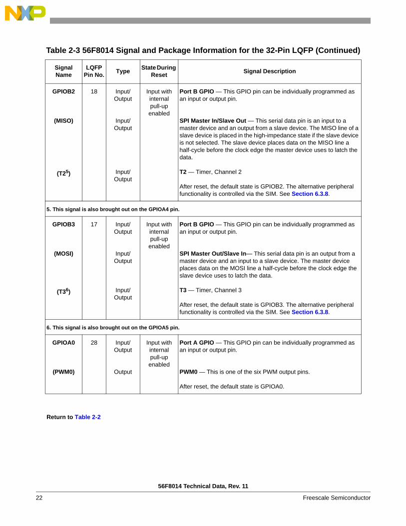
GPIOB2
(MISO)
(T25)
18 Input/Output
Input/Output
Input/Output
Input with internal pull-up
enabled
Port B GPIO — This GPIO pin can be individually programmed as an input or output pin.
SPI Master In/Slave Out — This serial data pin is an input to a master device and an output from a slave device. The MISO line of a slave device is placed in the high-impedance state if the slave device is not selected. The slave device places data on the MISO line a half-cycle before the clock edge the master device uses to latch the data.
T2 — Timer, Channel 2
After reset, the default state is GPIOB2. The alternative peripheral functionality is controlled via the SIM. See Section 6.3.8.
5. This signal is also brought out on the GPIOA4 pin.
GPIOB3
(MOSI)
(T36)
17 Input/Output
Input/Output
Input/Output
Input with internal pull-up
enabled
Port B GPIO — This GPIO pin can be individually programmed as an input or output pin.
SPI Master Out/Slave In— This serial data pin is an output from a master device and an input to a slave device. The master device places data on the MOSI line a half-cycle before the clock edge the slave device uses to latch the data.
T3 — Timer, Channel 3
After reset, the default state is GPIOB3. The alternative peripheral functionality is controlled via the SIM. See Section 6.3.8.
6. This signal is also brought out on the GPIOA5 pin.
GPIOA0
(PWM0)
28 Input/Output
Output
Input with internal pull-up
enabled
Port A GPIO — This GPIO pin can be individually programmed as an input or output pin.
PWM0 — This is one of the six PWM output pins.
After reset, the default state is GPIOA0.
Return to Table 2-2
Table 2-3 56F8014 Signal and Package Information for the 32-Pin LQFP (Continued)
Signal Name
LQFP Pin No. Type State During
Reset Signal Description

56F8014 Signal Pins
56F8014 Technical Data, Rev. 11
Freescale Semiconductor 23
GPIOA1
(PWM1)
27 Input/Output
Output
Input with internal pull-up
enabled
Port A GPIO — This GPIO pin can be individually programmed as an input or output pin.
PWM1 — This is one of the six PWM output pins.
After reset, the default state is GPIOA1.
GPIOA2
(PWM2)
23 Input/Output
Output
Input with internal pull-up
enabled
Port A GPIO — This GPIO pin can be individually programmed as an input or output pin.
PWM2 — This is one of the six PWM output pins.
After reset, the default state is GPIOA2.
GPIOA4
(PWM4)
(FAULT1)
(T27)
22 Input/Output
Output
Input
Input/Output
Input with internal pull-up
enabled
Port A GPIO — This GPIO pin can be individually programmed as an input or output pin.
PWM4 — This is one of the six PWM output pins.
Fault1 — This fault input pin is used for disabling selected PWM outputs in cases where fault conditions originate off-chip.
T2 — Timer, Channel 2
After reset, the default state is GPIOA4. The alternative peripheral functionality is controlled via the SIM. See Section 6.3.8.
7. This signal is also brought out on the GPIOB2 pin.
GPIOA5
(PWM5)
(FAULT2)
(T38)
20 Input/Output
Output
Input
Input/Output
Input with internal pull-up
enabled
Port A GPIO — This GPIO pin can be individually programmed as an input or output pin.
PWM5 — This is one of the six PWM output pins.
Fault2 — This fault input pin is used for disabling selected PWM outputs in cases where fault conditions originate off-chip.
T3 — Timer, Channel 3
After reset, the default state is GPIOA5. The alternative peripheral functionality is controlled via the SIM. See Section 6.3.8.
8. This signal is also brought out on the GPIOB3 pin.
Return to Table 2-2
Table 2-3 56F8014 Signal and Package Information for the 32-Pin LQFP (Continued)
Signal Name
LQFP Pin No. Type State During
Reset Signal Description
56F8014 Technical Data, Rev. 11
24 Freescale Semiconductor
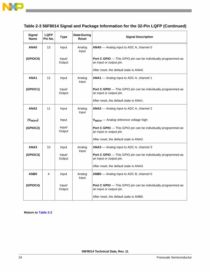
ANA0
(GPIOC0)
13 Input
Input/Output
Analog Input
ANA0 — Analog input to ADC A, channel 0
Port C GPIO — This GPIO pin can be individually programmed as an input or output pin.
After reset, the default state is ANA0.
ANA1
(GPIOC1)
12 Input
Input/Output
Analog Input
ANA1 — Analog input to ADC A, channel 1
Port C GPIO — This GPIO pin can be individually programmed as an input or output pin.
After reset, the default state is ANA1.
ANA2
(VREFH)
(GPIOC2)
11 Input
Input
Input/Output
Analog Input
ANA2 — Analog input to ADC A, channel 2
VREFH — Analog reference voltage high
Port C GPIO — This GPIO pin can be individually programmed as an input or output pin.
After reset, the default state is ANA2.
ANA3
(GPIOC3)
10 Input
Input/Output
Analog Input
ANA3 — Analog input to ADC A, channel 3
Port C GPIO — This GPIO pin can be individually programmed as an input or output pin.
After reset, the default state is ANA3.
ANB0
(GPIOC4)
4 Input
Input/Output
Analog Input
ANB0 — Analog input to ADC B, channel 0
Port C GPIO — This GPIO pin can be individually programmed as an input or output pin.
After reset, the default state is ANB0.
Return to Table 2-2
Table 2-3 56F8014 Signal and Package Information for the 32-Pin LQFP (Continued)
Signal Name
LQFP Pin No. Type State During
Reset Signal Description

56F8014 Signal Pins
56F8014 Technical Data, Rev. 11
Freescale Semiconductor 25
ANB1
(GPIOC5)
5 Input
Input/Output
Analog Input
ANB1 — Analog input to ADC B, channel 1
Port C GPIO — This GPIO pin can be individually programmed as an input or output pin.
After reset, the default state is ANB1.
ANB2
(VREFL)
(GPIOC6)
6 Input
Input
Input/Output
Analog Input
ANB2 — Analog input to ADC B, channel 2
VREFL — Analog reference voltage low. This should normally be connected to a low-noise VSS.
Port C GPIO — This GPIO pin can be individually programmed as an input or output pin.
After reset, the default state is ANB2.
ANB3
(GPIOC7)
7 Input
Input/Output
Analog Input
ANB3 — Analog input to ADC B, channel 3
Port C GPIO — This GPIO pin can be individually programmed as an input or output pin.
After reset, the default state is ANB3.
Return to Table 2-2
Table 2-3 56F8014 Signal and Package Information for the 32-Pin LQFP (Continued)
Signal Name
LQFP Pin No. Type State During
Reset Signal Description

56F8014 Technical Data, Rev. 11
26 Freescale Semiconductor
Part 3 OCCS
3.1 OverviewThis module provides the system clock, which uses it to generate the various chip clocks. This module alsoproduces the oscillator clock signals, plus the ADC clock and high-speed peripheral clock.
The on-chip clock synthesis module allows product design using an internal relaxation oscillator to run56F801X family parts at user-selectable frequencies up to 32MHz.
3.2 FeaturesThe On-Chip Clock Synthesis (OCCS) module interfaces to the oscillator and PLL. The OCCS modulefeatures:
• Internal relaxation oscillator• Ability to power down the internal relaxation oscillator• Ability to put the internal relaxation oscillator into a standby mode• 3-bit postscaler provides control for the PLL output• Ability to power down the internal PLL• Provides 2X system clock frequency, which operates at twice the system clock, to the System Integration
Module (SIM) that is used to generate the various device clocks• Provides 3X system clock, which operates at three times the system clock, to PWM and Timer• Safety shutdown feature is available in the event that the PLL reference clock disappears• Can be driven from an external clock source
The clock generation module provides the programming interface for both the PLL and internal relaxationoscillator.
3.3 Operating ModesIn 56F801X family parts, either an internal oscillator or an external frequency source can be used toprovide a reference clock to the SIM.
The 2X system clock source output from the OCCS can be described by one of the following equations:
2X system frequency = oscillator frequency
2X system frequency = (oscillator frequency X 8) / (postscaler)
where:
postscaler = 1, 2, 4, 8, 16, or 32 PLL output divider
The SIM is responsible for further dividing these frequencies by two, which will insure a 50% duty cyclein the system clock output.

Operating Modes
56F8014 Technical Data, Rev. 11
Freescale Semiconductor 27
The 56F801X family parts’ on-chip clock synthesis module has the following registers:
• Control Register (OCCS_CR)• Divide-by Register (OCCS_DB)• Status Register (OCCS_SR)• Shutdown Register (OCCS_SHUTDN)• Oscillator Control Register (OCCS_OCTRL)
For more information on these registers, please refer to the 56F801X Peripheral Reference Manual.
3.3.1 External Clock SourceThe recommended method of connecting an external clock is illustrated in Figure 3-1. The external clocksource is connected to GPIOB6 / RXD / SDA / CLKIN.
Figure 3-1 Connecting an External Clock Signal using GPIOB6 / RXD / SDA / CLKIN
56F8014GPIOB6/RXD/SDA/CLKIN
External Clock

56F8014 Technical Data, Rev. 11
28 Freescale Semiconductor
3.4 Block DiagramFigure 3-2 provides a block diagram which shows how the 56F8014 creates its internal clock, using therelaxation oscillator as an 8MHz clock reference for the PLL.
Figure 3-2 OCCS Block Diagram with Relaxation Oscillator
TRIM[9:0]
ROSB
ROPD
Relaxation OSC
Bus Interface and Control
BusInterface GPIOB6 / RXD
PRECSMUX
MU
XM
UX
MSTR_OSC
SYS_CLK_x2source to the SIM
(64MHz max)
ZSRC
HS PERF CLK
(96MHz max)
Postscaler(÷ 1, 2, 4, 8, 16, 32)
Postscaler(÷ 1, 2, 4, 8, 16, 32)
÷ 3
÷ 2
PLLX 24
Lock Detector
Loss of Reference
Clock Detector
Loss of Reference Clock Interrupt
LCKF OU
T/2
FEE
DBA
CK
PLLCOD
FOUT

Pin Descriptions
56F8014 Technical Data, Rev. 11
Freescale Semiconductor 29
3.5 Pin Descriptions
3.5.1 External Reference (GPIOB6 / RXD / SDA / CLKIN)After reset, the internal relaxation oscillator is selected as the clock source for the chip. The user then hasthe option of switching to an external clock reference by enabling the PRECS bit in the OCCS OscillatorControl register, if desired.
Part 4 Memory Map4.1 IntroductionThe 56F8014 device is a 16-bit motor-control chip based on the 56800E core. It uses a Harvard-stylearchitecture with two independent memory spaces for Data and Program. On-chip RAM is used in bothspaces and Flash memory is used only in Program space.
This section provides memory maps for:
• Program Address Space, including the Interrupt Vector Table• Data Address Space, including the EOnCE Memory and Peripheral Memory Maps
On-chip memory sizes for the device are summarized in Table 4-1. Flash memories’ restrictions areidentified in the “Use Restrictions” column of Table 4-1.
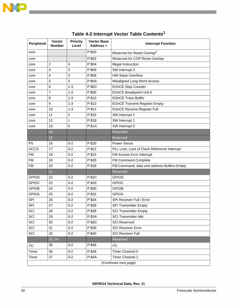
4.2 Interrupt Vector TableTable 4-2 provides the 56F8014’s reset and interrupt priority structure, including on-chip peripherals. Thetable is organized with higher-priority vectors at the top and lower-priority interrupts lower in the table.As indicated, the priority of an interrupt can be assigned to different levels, allowing some control overinterrupt priorities. All level 3 interrupts will be serviced before level 2, and so on. For a selected prioritylevel, the lowest vector number has the highest priority.
The location of the vector table is determined by the Vector Base Address (VBA). Please see Section 5.5.6for the reset value of the VBA.
By default, the chip reset address and COP reset address will correspond to vector 0 and 1 of the interruptvector table. In these instances, the first two locations in the vector table must contain branch or JMPinstructions. All other entries must contain JSR instructions.
Table 4-1 Chip Memory Configurations
On-Chip Memory 56F8014 Use Restrictions
Program Flash (PFLASH)
8k x 16 Erase / Program via Flash interface unit and word writes to CDBW
Unified RAM (ram) 2k x 16 Usable by both the Program and Data memory spaces
56F8014 Technical Data, Rev. 11
30 Freescale Semiconductor
Table 4-2 Interrupt Vector Table Contents1
Peripheral Vector Number
Priority Level
Vector Base Address + Interrupt Function
core P:$00 Reserved for Reset Overlay2 core P:$02 Reserved for COP Reset Overlaycore 2 3 P:$04 Illegal Instruction core 3 3 P:$06 SW Interrupt 3core 4 3 P:$08 HW Stack Overflowcore 5 3 P:$0A Misaligned Long Word Accesscore 6 1-3 P:$0C EOnCE Step Countercore 7 1-3 P:$0E EOnCE Breakpoint Unit 0core 8 1-3 P:$10 EOnCE Trace Buffercore 9 1-3 P:$12 EOnCE Transmit Register Emptycore 10 1-3 P:$14 EOnCE Receive Register Fullcore 11 2 P:$16 SW Interrupt 2core 12 1 P:$18 SW Interrupt 1core 13 0 P:$1A SW Interrupt 0
14 Reserved
15 ReservedPS 16 0-2 P:$20 Power SenseOCCS 17 0-2 P:$22 PLL Lock, Loss of Clock Reference InterruptFM 18 0-2 P:$24 FM Access Error InterruptFM 19 0-2 P:$26 FM Command Complete FM 20 0-2 P:$28 FM Command, data and address Buffers Empty
21 ReservedGPIOD 22 0-2 P:$2C GPIODGPIOC 23 0-2 P:$2E GPIOCGPIOB 24 0-2 P:$30 GPIOBGPIOA 25 0-2 P:$32 GPIOASPI 26 0-2 P:$34 SPI Receiver Full / ErrorSPI 27 0-2 P:$36 SPI Transmitter EmptySCI 28 0-2 P:$38 SCI Transmitter EmptySCI 29 0-2 P:$3A SCI Transmitter IdleSCI 30 0-2 P:$3C SCI ReservedSCI 31 0-2 P:$3E SCI Receiver ErrorSCI 32 0-2 P:$40 SCI Receiver Full
33, 34 Reserved
I2C 35 0-2 P:$46 I2C Timer 36 0-2 P:$48 Timer Channel 0Timer 37 0-2 P:$4A Timer Channel 1
(Continues next page)
Program Map
56F8014 Technical Data, Rev. 11
Freescale Semiconductor 31
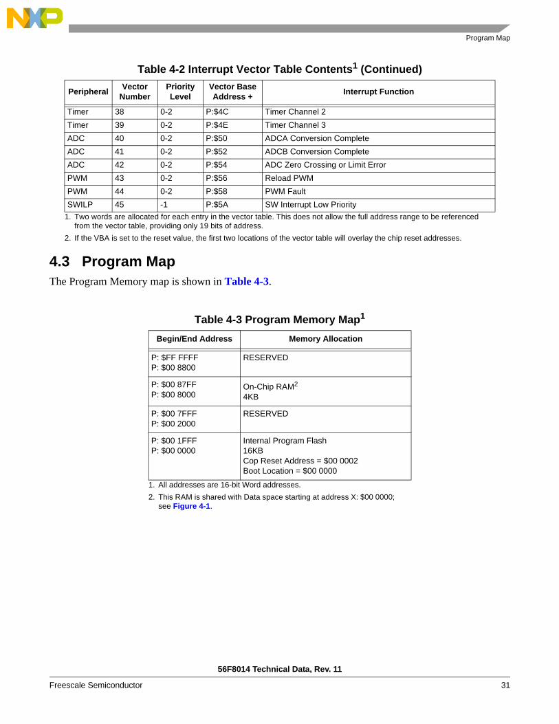
4.3 Program MapThe Program Memory map is shown in Table 4-3.
Timer 38 0-2 P:$4C Timer Channel 2Timer 39 0-2 P:$4E Timer Channel 3ADC 40 0-2 P:$50 ADCA Conversion CompleteADC 41 0-2 P:$52 ADCB Conversion CompleteADC 42 0-2 P:$54 ADC Zero Crossing or Limit ErrorPWM 43 0-2 P:$56 Reload PWMPWM 44 0-2 P:$58 PWM FaultSWILP 45 -1 P:$5A SW Interrupt Low Priority
1. Two words are allocated for each entry in the vector table. This does not allow the full address range to be referencedfrom the vector table, providing only 19 bits of address.
2. If the VBA is set to the reset value, the first two locations of the vector table will overlay the chip reset addresses.
Table 4-3 Program Memory Map1
1. All addresses are 16-bit Word addresses.
Begin/End Address Memory Allocation
P: $FF FFFFP: $00 8800
RESERVED
P: $00 87FFP: $00 8000
On-Chip RAM2
4KB
2. This RAM is shared with Data space starting at address X: $00 0000;see Figure 4-1.
P: $00 7FFFP: $00 2000
RESERVED
P: $00 1FFFP: $00 0000
Internal Program Flash 16KBCop Reset Address = $00 0002Boot Location = $00 0000
Table 4-2 Interrupt Vector Table Contents1 (Continued)
Peripheral Vector Number
Priority Level
Vector Base Address + Interrupt Function

56F8014 Technical Data, Rev. 11
32 Freescale Semiconductor
4.4 Data Map
Figure 4-1 Dual Port RAM
4.5 EOnCE Memory MapFigure 4-5 lists all EOnCE registers necessary to access or control the EOnCE.
Table 4-4 Data Memory Map1
1. All addresses are 16-bit Word addresses.
Begin/End Address Memory Allocation
X:$FF FFFFX:$FF FF00
EOnCE256 locations allocated
X:$FF FEFFX:$01 0000 RESERVED
X:$00 FFFFX:$00 F000
On-Chip Peripherals4096 locations allocated
X:$00 EFFFX:$00 8800
RESERVED
X:$00 EFFFX:$00 0800
Reserved
X:$00 7FFFX:$00 0040
RESERVED
X:$00 07FFX:$00 0000
On-Chip Data RAM2
4KB
2. This RAM is shared with Program space starting at P: $00 8000; seeFigure 4-1.
Reserved
RAM
Reserved
Flash
Reserved
EOnCE
Peripherals
Reserved
RAM
Dual Port RAM
Program Data
Peripheral Memory Mapped Registers
56F8014 Technical Data, Rev. 11
Freescale Semiconductor 33
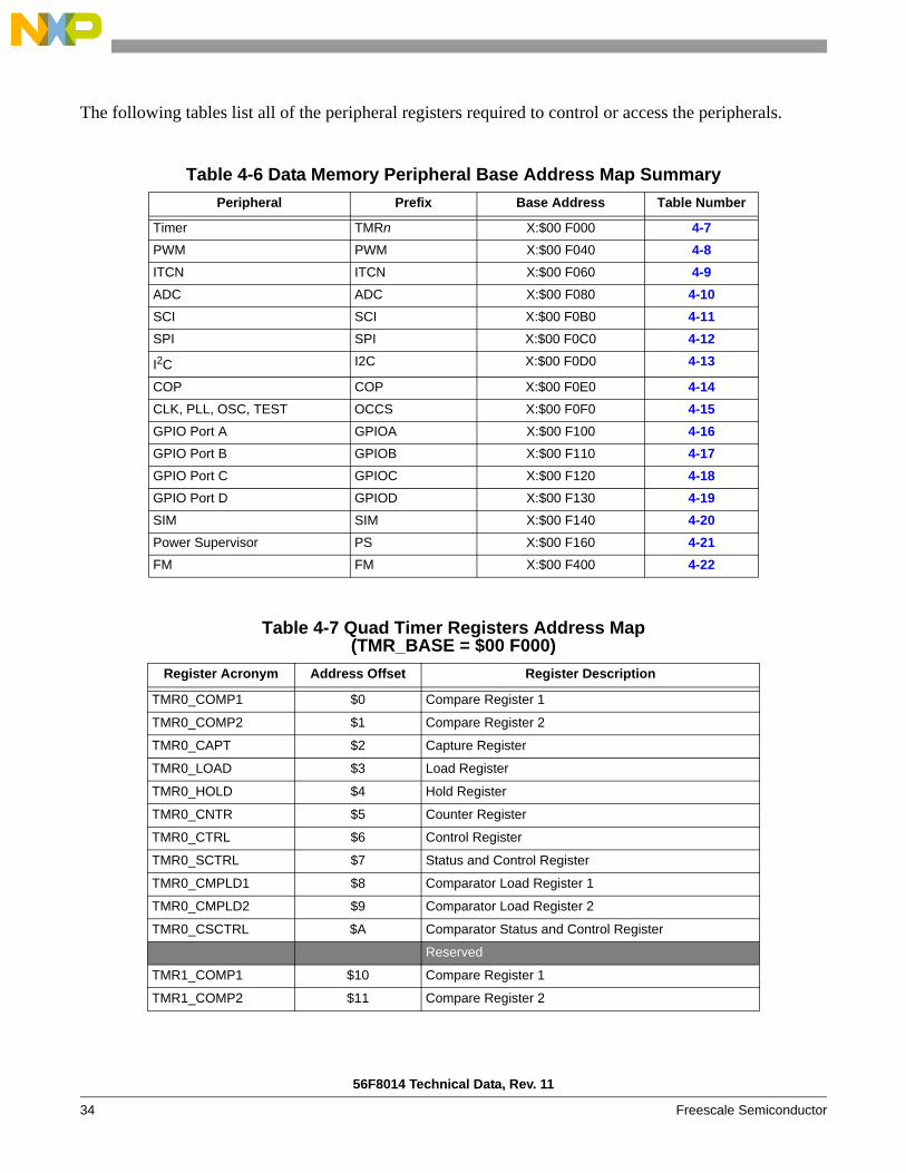
4.6 Peripheral Memory Mapped RegistersOn-chip peripheral registers are part of the data memory map on the 56800E series. These locations maybe accessed with the same addressing modes used for ordinary Data memory, except all peripheralregisters should be read/written using word accesses only.
Table 4-6 summarizes base addresses for the set of peripherals on the 56F8014 device. Peripherals arelisted in order of the base address.
Table 4-5 EOnCE Memory Map Address Register Acronym Register Name
X:$FF FFFF OTX1 / ORX1 Transmit Register Upper WordReceive Register Upper Word
X:$FF FFFE OTX / ORX (32 bits) Transmit RegisterReceive Register
X:$FF FFFD OTXRXSR Transmit and Receive Status and Control Register
X:$FF FFFC OCLSR Core Lock / Unlock Status Register
X:$FF FFFB - X:$FF FFA1 Reserved
X:$FF FFA0 OCR Control Register
X:$FF FF9F Instruction Step Counter
X:$FF FF9E OSCNTR (24 bits) Instruction Step Counter
X:$FF FF9D OSR Status Register
X:$FF FF9C OBASE Peripheral Base Address Register
X:$FF FF9B OTBCR Trace Buffer Control Register
X:$FF FF9A OTBPR Trace Buffer Pointer Register
X:$FF FF99 Trace Buffer Register Stages
X:$FF FF98 OTB (21 - 24 bits/stage) Trace Buffer Register Stages
X:$FF FF97 Breakpoint Unit Control Register
X:$FF FF96 OBCR (24 bits) Breakpoint Unit Control Register
X:$FF FF95 Breakpoint Unit Address Register 1
X:$FF FF94 OBAR1 (24 bits) Breakpoint Unit Address Register 1
X:$FF FF93 Breakpoint Unit Address Register 2
X:$FF FF92 OBAR2 (32 bits) Breakpoint Unit Address Register 2
X:$FF FF91 Breakpoint Unit Mask Register 2
X:$FF FF90 OBMSK (32 bits) Breakpoint Unit Mask Register 2
X:$FF FF8F Reserved
X:$FF FF8E OBCNTR EOnCE Breakpoint Unit Counter
X:$FF FF8D Reserved
X:$FF FF8C Reserved
X:$FF FF8B Reserved
X:$FF FF8A OESCR External Signal Control Register
X:$FF FF89 - X:$FF FF00 Reserved
56F8014 Technical Data, Rev. 11
34 Freescale Semiconductor
The following tables list all of the peripheral registers required to control or access the peripherals.
Table 4-6 Data Memory Peripheral Base Address Map SummaryPeripheral Prefix Base Address Table Number
Timer TMRn X:$00 F000 4-7PWM PWM X:$00 F040 4-8ITCN ITCN X:$00 F060 4-9ADC ADC X:$00 F080 4-10SCI SCI X:$00 F0B0 4-11SPI SPI X:$00 F0C0 4-12
I2C I2C X:$00 F0D0 4-13
COP COP X:$00 F0E0 4-14CLK, PLL, OSC, TEST OCCS X:$00 F0F0 4-15GPIO Port A GPIOA X:$00 F100 4-16GPIO Port B GPIOB X:$00 F110 4-17GPIO Port C GPIOC X:$00 F120 4-18GPIO Port D GPIOD X:$00 F130 4-19SIM SIM X:$00 F140 4-20Power Supervisor PS X:$00 F160 4-21FM FM X:$00 F400 4-22
Table 4-7 Quad Timer Registers Address Map(TMR_BASE = $00 F000)
Register Acronym Address Offset Register Description
TMR0_COMP1 $0 Compare Register 1
TMR0_COMP2 $1 Compare Register 2
TMR0_CAPT $2 Capture Register
TMR0_LOAD $3 Load Register
TMR0_HOLD $4 Hold Register
TMR0_CNTR $5 Counter Register
TMR0_CTRL $6 Control Register
TMR0_SCTRL $7 Status and Control Register
TMR0_CMPLD1 $8 Comparator Load Register 1
TMR0_CMPLD2 $9 Comparator Load Register 2
TMR0_CSCTRL $A Comparator Status and Control Register
Reserved
TMR1_COMP1 $10 Compare Register 1
TMR1_COMP2 $11 Compare Register 2

Peripheral Memory Mapped Registers
56F8014 Technical Data, Rev. 11
Freescale Semiconductor 35
TMR1_CAPT $12 Capture Register
TMR1_LOAD $13 Load Register
TMR1_HOLD $14 Hold Register
TMR1_CNTR $15 Counter Register
TMR1_CTRL $16 Control Register
TMR1_SCTRL $17 Status and Control Register
TMR1_CMPLD1 $18 Comparator Load Register 1
TMR1_CMPLD2 $19 Comparator Load Register 2
TMR1_CSCTRL $1A Comparator Status and Control Register
Reserved
TMR2_COMP1 $20 Compare Register 1
TMR2_COMP2 $21 Compare Register 2
TMR2_CAPT $22 Capture Register
TMR2_LOAD $23 Load Register
TMR2_HOLD $24 Hold Register
TMR2_CNTR $25 Counter Register
TMR2_CTRL $26 Control Register
TMR2_SCTRL $27 Status and Control Register
TMR2_CMPLD1 $28 Comparator Load Register 1
TMR2_CMPLD2 $29 Comparator Load Register 2
TMR2_CSCTRL $2A Comparator Status and Control Register
Reserved
TMR3_COMP1 $30 Compare Register 1
TMR3_COMP2 $31 Compare Register 2
TMR3_CAPT $32 Capture Register
TMR3_LOAD $33 Load Register
TMR3_HOLD $34 Hold Register
TMR3_CNTR $35 Counter Register
TMR3_CTRL $36 Control Register
TMR3_SCTRL $37 Status and Control Register
TMR3_CMPLD1 $38 Comparator Load Register 1
TMR3_CMPLD2 $39 Comparator Load Register 2
TMR3_CSCTRL $3A Comparator Status and Control Register
Table 4-7 Quad Timer Registers Address Map (Continued)(TMR_BASE = $00 F000)
Register Acronym Address Offset Register Description

56F8014 Technical Data, Rev. 11
36 Freescale Semiconductor
Table 4-8 Pulse Width Modulator Registers Address Map(PWM_BASE = $00 F040)
Register Acronym Address Offset Register Description
PWM_CTRL $0 Control Register
PWM_FCTRL $1 Fault Control Register
PWM_FLTACK $2 Fault Status Acknowledge Register
PWM_OUT $3 Output Control Register
PWM_CNTR $4 Counter Register
PWM_CMOD $5 Counter Modulo Register
PWM_VAL0 $6 Value Register 0
PWM_VAL1 $7 Value Register 1
PWM_VAL2 $8 Value Register 2
PWM_VAL3 $9 Value Register 3
PWM_VAL4 $A Value Register 4
PWM_VAL5 $B Value Register 5
PWM_DTIM0 $C Dead Time Register 0
PWM_DTIM1 $D Dead Time Register 1
PWM_DMAP1 $E Disable Mapping Register 1
PWM_DMAP2 $F Disable Mapping Register 2
PWM_CNFG $10 Configure Register
PWM_CCTRL $11 Channel Control Register
PWM_PORT $12 Port Register
PWM_ICCTRL $13 Internal Correction Control Register
PWM_SCTRL $14 Source Control Register
Table 4-9 Interrupt Control Registers Address Map(ITCN_BASE = $00 F060)
Register Acronym Address Offset Register Description
ITCN_IPR0 $0 Interrupt Priority Register 0
ITCN_IPR1 $1 Interrupt Priority Register 1
ITCN_IPR2 $2 Interrupt Priority Register 2
ITCN_IPR3 $3 Interrupt Priority Register 3
ITCN_IPR4 $4 Interrupt Priority Register 4
ITCN_VBA $5 Vector Base Address Register
ITCN_FIM0 $6 Fast Interrupt Match 0 Register
ITCN_FIVAL0 $7 Fast Interrupt Vector Address Low 0 Register
ITCN_FIVAH0 $8 Fast Interrupt Vector Address High 0 Register

Peripheral Memory Mapped Registers
56F8014 Technical Data, Rev. 11
Freescale Semiconductor 37
ITCN_FIM1 $9 Fast Interrupt Match 1 Register
ITCN_FIVAL1 $A Fast Interrupt Vector Address Low 1 Register
ITCN_FIVAH1 $B Fast Interrupt Vector Address High 1 Register
ITCN_IRQP 0 $C IRQ Pending Register 0
ITCN_IRQP 1 $D IRQ Pending Register 1
ITCN_IRQP 2 $E IRQ Pending Register 2
Reserved
ITCN_ICTRL $12 Interrupt Control Register
Reserved
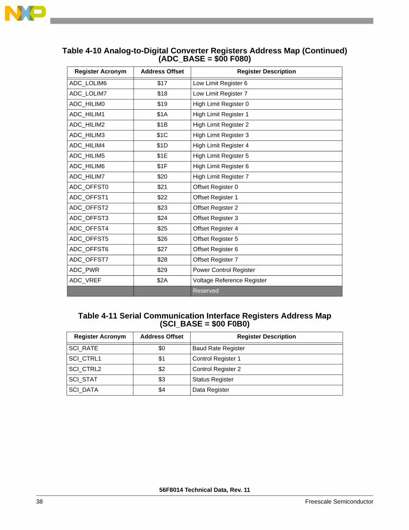
Table 4-10 Analog-to-Digital Converter Registers Address Map(ADC_BASE = $00 F080)
Register Acronym Address Offset Register Description
ADC_CTRL1 $0 Control Register 1
ADC_CTRL2 $1 Control Register 2
ADC_ZXCTRL $2 Zero Crossing Control Register
ADC_CLIST 1 $3 Channel List Register 1
ADC_CLIST 2 $4 Channel List Register 2
ADC_SDIS $5 Sample Disable Register
ADC_STAT $6 Status Register
ADC_LIMSTAT $7 Limit Status Register
ADC_ZXSTAT $8 Zero Crossing Status Register
ADC_RSLT0 $9 Result Register 0
ADC_RSLT1 $A Result Register 1
ADC_RSLT2 $B Result Register 2
ADC_RSLT3 $C Result Register 3
ADC_RSLT4 $D Result Register 4
ADC_RSLT5 $E Result Register 5
ADC_RSLT6 $F Result Register 6
ADC_RSLT7 $10 Result Register 7
ADC_LOLIM0 $11 Low Limit Register 0
ADC_LOLIM1 $12 Low Limit Register 1
ADC_LOLIM2 $13 Low Limit Register 2
ADC_LOLIM3 $14 Low Limit Register 3
ADC_LOLIM4 $15 Low Limit Register 4
ADC_LOLIM5 $16 Low Limit Register 5
Table 4-9 Interrupt Control Registers Address Map (Continued)(ITCN_BASE = $00 F060)
Register Acronym Address Offset Register Description
56F8014 Technical Data, Rev. 11
38 Freescale Semiconductor
ADC_LOLIM6 $17 Low Limit Register 6
ADC_LOLIM7 $18 Low Limit Register 7
ADC_HILIM0 $19 High Limit Register 0
ADC_HILIM1 $1A High Limit Register 1
ADC_HILIM2 $1B High Limit Register 2
ADC_HILIM3 $1C High Limit Register 3
ADC_HILIM4 $1D High Limit Register 4
ADC_HILIM5 $1E High Limit Register 5
ADC_HILIM6 $1F High Limit Register 6
ADC_HILIM7 $20 High Limit Register 7
ADC_OFFST0 $21 Offset Register 0
ADC_OFFST1 $22 Offset Register 1
ADC_OFFST2 $23 Offset Register 2
ADC_OFFST3 $24 Offset Register 3
ADC_OFFST4 $25 Offset Register 4
ADC_OFFST5 $26 Offset Register 5
ADC_OFFST6 $27 Offset Register 6
ADC_OFFST7 $28 Offset Register 7
ADC_PWR $29 Power Control Register
ADC_VREF $2A Voltage Reference Register
Reserved
Table 4-11 Serial Communication Interface Registers Address Map(SCI_BASE = $00 F0B0)
Register Acronym Address Offset Register Description
SCI_RATE $0 Baud Rate Register
SCI_CTRL1 $1 Control Register 1
SCI_CTRL2 $2 Control Register 2
SCI_STAT $3 Status Register
SCI_DATA $4 Data Register
Table 4-10 Analog-to-Digital Converter Registers Address Map (Continued)(ADC_BASE = $00 F080)
Register Acronym Address Offset Register Description
Peripheral Memory Mapped Registers
56F8014 Technical Data, Rev. 11
Freescale Semiconductor 39
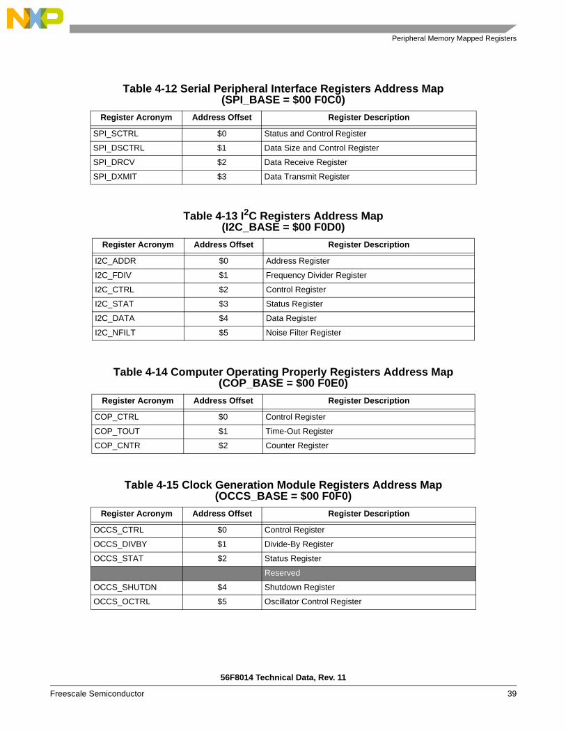
Table 4-12 Serial Peripheral Interface Registers Address Map(SPI_BASE = $00 F0C0)
Register Acronym Address Offset Register Description
SPI_SCTRL $0 Status and Control Register
SPI_DSCTRL $1 Data Size and Control Register
SPI_DRCV $2 Data Receive Register
SPI_DXMIT $3 Data Transmit Register
Table 4-13 I2C Registers Address Map(I2C_BASE = $00 F0D0)
Register Acronym Address Offset Register Description
I2C_ADDR $0 Address Register
I2C_FDIV $1 Frequency Divider Register
I2C_CTRL $2 Control Register
I2C_STAT $3 Status Register
I2C_DATA $4 Data Register
I2C_NFILT $5 Noise Filter Register
Table 4-14 Computer Operating Properly Registers Address Map(COP_BASE = $00 F0E0)
Register Acronym Address Offset Register Description
COP_CTRL $0 Control Register
COP_TOUT $1 Time-Out Register
COP_CNTR $2 Counter Register
Table 4-15 Clock Generation Module Registers Address Map(OCCS_BASE = $00 F0F0)
Register Acronym Address Offset Register Description
OCCS_CTRL $0 Control Register
OCCS_DIVBY $1 Divide-By Register
OCCS_STAT $2 Status Register
Reserved
OCCS_SHUTDN $4 Shutdown Register
OCCS_OCTRL $5 Oscillator Control Register

56F8014 Technical Data, Rev. 11
40 Freescale Semiconductor
Table 4-16 GPIOA Registers Address Map(GPIOA_BASE = $00 F100)
Register Acronym Address Offset Register Description
GPIOA_PUPEN $0 Pull-up Enable Register
GPIOA_DATA $1 Data Register
GPIOA_DDIR $2 Data Direction Register
GPIOA_PEREN $3 Peripheral Enable Register
GPIOA_IASSRT $4 Interrupt Assert Register
GPIOA_IEN $5 Interrupt Enable Register
GPIOA_IEPOL $6 Interrupt Edge Polarity Register
GPIOA_IPEND $7 Interrupt Pending Register
GPIOA_IEDGE $8 Interrupt Edge-Sensitive Register
GPIOA_PPOUTM $9 Push-Pull Output Mode Control Register
GPIOA_RDATA $A Raw Data Register
GPIOA_DRIVE $B Drive Strength Control Register
Table 4-17 GPIOB Registers Address Map(GPIOB_BASE = $00 F110)
Register Acronym Address Offset Register Description
GPIOB_PUPEN $0 Pull-up Enable Register
GPIOB_DATA $1 Data Register
GPIOB_DDIR $2 Data Direction Register
GPIOB_PEREN $3 Peripheral Enable Register
GPIOB_IASSRT $4 Interrupt Assert Register
GPIOB_IEN $5 Interrupt Enable Register
GPIOB_IEPOL $6 Interrupt Edge Polarity Register
GPIOB_IPEND $7 Interrupt Pending Register
GPIOB_IEDGE $8 Interrupt Edge-Sensitive Register
GPIOB_PPOUTM $9 Push-Pull Output Mode Control Register
GPIOB_RDATA $A Raw Data Register
GPIOB_DRIVE $B Drive Strength Control Register
Peripheral Memory Mapped Registers
56F8014 Technical Data, Rev. 11
Freescale Semiconductor 41
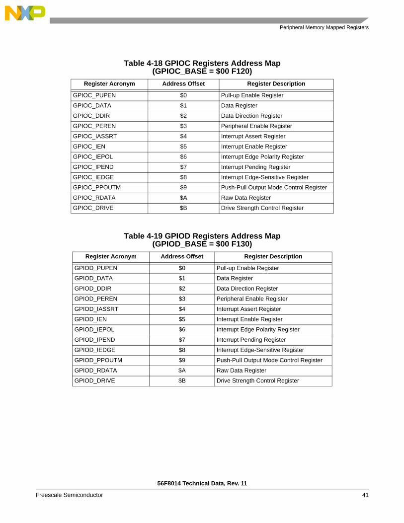
Table 4-18 GPIOC Registers Address Map(GPIOC_BASE = $00 F120)
Register Acronym Address Offset Register Description
GPIOC_PUPEN $0 Pull-up Enable Register
GPIOC_DATA $1 Data Register
GPIOC_DDIR $2 Data Direction Register
GPIOC_PEREN $3 Peripheral Enable Register
GPIOC_IASSRT $4 Interrupt Assert Register
GPIOC_IEN $5 Interrupt Enable Register
GPIOC_IEPOL $6 Interrupt Edge Polarity Register
GPIOC_IPEND $7 Interrupt Pending Register
GPIOC_IEDGE $8 Interrupt Edge-Sensitive Register
GPIOC_PPOUTM $9 Push-Pull Output Mode Control Register
GPIOC_RDATA $A Raw Data Register
GPIOC_DRIVE $B Drive Strength Control Register
Table 4-19 GPIOD Registers Address Map(GPIOD_BASE = $00 F130)
Register Acronym Address Offset Register Description
GPIOD_PUPEN $0 Pull-up Enable Register
GPIOD_DATA $1 Data Register
GPIOD_DDIR $2 Data Direction Register
GPIOD_PEREN $3 Peripheral Enable Register
GPIOD_IASSRT $4 Interrupt Assert Register
GPIOD_IEN $5 Interrupt Enable Register
GPIOD_IEPOL $6 Interrupt Edge Polarity Register
GPIOD_IPEND $7 Interrupt Pending Register
GPIOD_IEDGE $8 Interrupt Edge-Sensitive Register
GPIOD_PPOUTM $9 Push-Pull Output Mode Control Register
GPIOD_RDATA $A Raw Data Register
GPIOD_DRIVE $B Drive Strength Control Register
56F8014 Technical Data, Rev. 11
42 Freescale Semiconductor
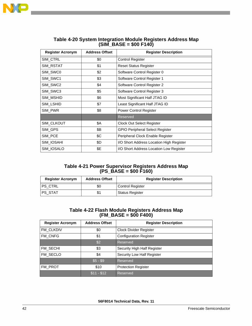
Table 4-20 System Integration Module Registers Address Map(SIM_BASE = $00 F140)
Register Acronym Address Offset Register Description
SIM_CTRL $0 Control Register
SIM_RSTAT $1 Reset Status Register
SIM_SWC0 $2 Software Control Register 0
SIM_SWC1 $3 Software Control Register 1
SIM_SWC2 $4 Software Control Register 2
SIM_SWC3 $5 Software Control Register 3
SIM_MSHID $6 Most Significant Half JTAG ID
SIM_LSHID $7 Least Significant Half JTAG ID
SIM_PWR $8 Power Control Register
Reserved
SIM_CLKOUT $A Clock Out Select Register
SIM_GPS $B GPIO Peripheral Select Register
SIM_PCE $C Peripheral Clock Enable Register
SIM_IOSAHI $D I/O Short Address Location High Register
SIM_IOSALO $E I/O Short Address Location Low Register
Table 4-21 Power Supervisor Registers Address Map(PS_BASE = $00 F160)
Register Acronym Address Offset Register Description
PS_CTRL $0 Control Register
PS_STAT $1 Status Register
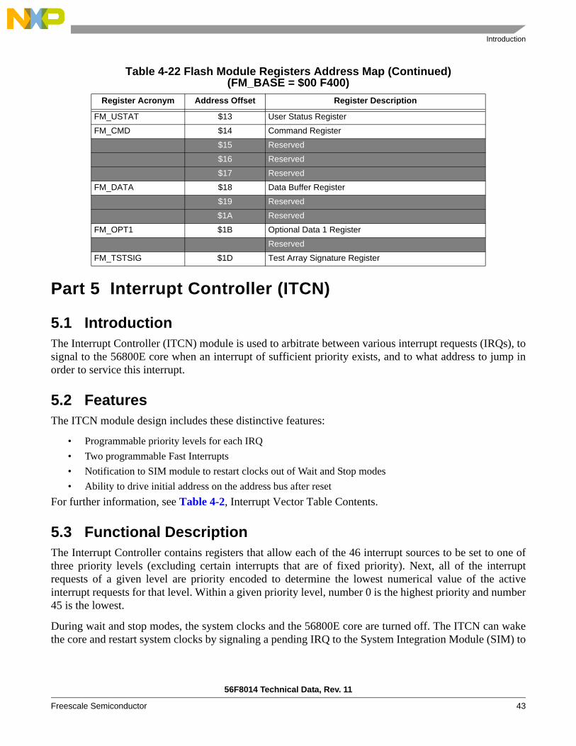
Table 4-22 Flash Module Registers Address Map(FM_BASE = $00 F400)
Register Acronym Address Offset Register Description
FM_CLKDIV $0 Clock Divider Register
FM_CNFG $1 Configuration Register
$2 Reserved
FM_SECHI $3 Security High Half Register
FM_SECLO $4 Security Low Half Register
$5 - $9 Reserved
FM_PROT $10 Protection Register
$11 - $12 Reserved
Introduction
56F8014 Technical Data, Rev. 11
Freescale Semiconductor 43
Part 5 Interrupt Controller (ITCN)
5.1 Introduction The Interrupt Controller (ITCN) module is used to arbitrate between various interrupt requests (IRQs), tosignal to the 56800E core when an interrupt of sufficient priority exists, and to what address to jump inorder to service this interrupt.
5.2 FeaturesThe ITCN module design includes these distinctive features:
• Programmable priority levels for each IRQ• Two programmable Fast Interrupts• Notification to SIM module to restart clocks out of Wait and Stop modes• Ability to drive initial address on the address bus after reset
For further information, see Table 4-2, Interrupt Vector Table Contents.
5.3 Functional DescriptionThe Interrupt Controller contains registers that allow each of the 46 interrupt sources to be set to one ofthree priority levels (excluding certain interrupts that are of fixed priority). Next, all of the interruptrequests of a given level are priority encoded to determine the lowest numerical value of the activeinterrupt requests for that level. Within a given priority level, number 0 is the highest priority and number45 is the lowest.
During wait and stop modes, the system clocks and the 56800E core are turned off. The ITCN can wakethe core and restart system clocks by signaling a pending IRQ to the System Integration Module (SIM) to
FM_USTAT $13 User Status Register
FM_CMD $14 Command Register
$15 Reserved
$16 Reserved
$17 Reserved
FM_DATA $18 Data Buffer Register
$19 Reserved
$1A Reserved
FM_OPT1 $1B Optional Data 1 Register
Reserved
FM_TSTSIG $1D Test Array Signature Register
Table 4-22 Flash Module Registers Address Map (Continued)(FM_BASE = $00 F400)
Register Acronym Address Offset Register Description

56F8014 Technical Data, Rev. 11
44 Freescale Semiconductor
restart the clocks and service the IRQ. An IRQ can only wake the core if the IRQ is enabled prior toentering wait or stop mode.
5.3.1 Normal Interrupt HandlingOnce the INTC has determined that an interrupt is to be serviced and which interrupt has the highestpriority, an interrupt vector address is generated. Normal interrupt handling concatenates the Vector BaseAddress (VBA) and the vector number to determine the vector address, generating an offset into the vectortable for each interrupt.
5.3.2 Interrupt NestingInterrupt exceptions may be nested to allow an IRQ of higher priority than the current exception to beserviced. The following table defines the nesting requirements for each priority level.
5.3.3 Fast Interrupt HandlingFast interrupts are described in the DSP56800E Reference Manual. The interrupt controller recognizesFast Interrupts before the core does.
A Fast Interrupt is defined (to the ITCN) by:
1. Setting the priority of the interrupt as level 2, with the appropriate field in the IPR registers2. Setting the FIMn register to the appropriate vector number
3. Setting the FIVALn and FIVAHn registers with the address of the code for the Fast InterruptWhen an interrupt occurs, its vector number is compared with the FIM0 and FIM1 register values. If amatch occurs, and it is a level 2 interrupt, the ITCN handles it as a Fast Interrupt. The ITCN takes the vectoraddress from the appropriate FIVALn and FIVAHn registers, instead of generating an address that is anoffset from the VBA.
The core then fetches the instruction from the indicated vector adddress and if it is not a JSR, the core startsits Fast Interrupt handling.
Table 5-1 Interrupt Mask Bit Definition
SR[9] SR[8] Exceptions Permitted Exceptions Masked
0 0 Priorities 0, 1, 2, 3 None
0 1 Priorities 1, 2, 3 Priority 0
1 0 Priorities 2, 3 Priorities 0, 1
1 1 Priority 3 Priorities 0, 1, 2

Block Diagram
56F8014 Technical Data, Rev. 11
Freescale Semiconductor 45
5.4 Block Diagram
Figure 5-1 Interrupt Controller Block Diagram
5.5 Register DescriptionsA register address is the sum of a base address and an address offset. The base address is defined at thesystem level and the address offset is defined at the module level. The ITCN module has 16 registers.
Table 5-2 ITCN Register Summary(ITCN_BASE = $00 F060)
Register Acronym Base Address + Register Name Section Location
IPR0 $0 Interrupt Priority Register 0 5.5.1
IPR1 $1 Interrupt Priority Register 1 5.5.2
IPR2 $2 Interrupt Priority Register 2 5.5.3
PriorityLevel
2 -> 4Decode
INT0
PriorityLevel
2 -> 4Decode
INT45
Level 0
46 -> 6PriorityEncoder
any0
Level 3
46 -> 6Priority
Encoder
any3
INT
VAB
IPICCONTROL
6
6 PIC_EN
IACK
SR[9:8]

56F8014 Technical Data, Rev. 11
46 Freescale Semiconductor
IPR3 $3 Interrupt Priority Register 3 5.5.4
IPR4 $4 Interrupt Priority Register 4 5.5.5
VBA $5 Vector Base Address Register 5.5.6
FIM0 $6 Fast Interrupt Match 0 Register 5.5.7
FIVAL0 $7 Fast Interrupt 0 Vector Address Low Register 5.5.8
FIVAH0 $8 Fast Interrupt 0 Vector Address High Register 5.5.9
FIM1 $9 Fast Interrupt Match 1 Register 5.5.10
FIVAL1 $A Fast Interrupt 1 Vector Address Low Register 5.5.11
FIVAH1 $B Fast Interrupt 1 Vector Address High Register 5.5.12
IRQP0 $C IRQ Pending Register 0 5.5.13
IRQP1 $D IRQ Pending Register 1 5.5.14
IRQP2 $E IRQ Pending Register 2 5.5.15
Reserved
ICTRL $12 Interrupt Control Register 5.5.16
Reserved
Table 5-2 ITCN Register Summary (Continued)(ITCN_BASE = $00 F060)
Register Acronym Base Address + Register Name Section Location

Register Descriptions
56F8014 Technical Data, Rev. 11
Freescale Semiconductor 47
Figure 5-2 ITCN Register Map Summary
5.5.1 Interrupt Priority Register 0 (IPR0)
Figure 5-3 Interrupt Priority Register 0 (IPR0)
Add. Offset
Register Name 15 14 13 12 11 10 9 8 7 6 5 4 3 2 1 0
$0 IPR0R
LVI IPL0 0 0 0
RX_REG IPL TX_REG IPL TRBUF IPL BKPT_U IPL STPCNT IPLW
$1 IPR1R
GPIOB IPL GPIOC IPL GPIOD IPL0 0
FM_CBE IPL FM_CC IPL FM_ERR IPL PLL IPLW
$2 IPR2R SCI_RCV
IPLSCI_RERR
IPL0 0
SCI_TIDL IPL SCI_XMIT IPL
SPI_XMIT IPL SPI_RCV IPL GPIOA IPL
W
$3 IPR3R ADCA_CC
IPL TMR_3 IPL TMR_2 IPL TMR_1 IPL TMR_0 IPL I2C_ADDR IPL
0 0 0 0
W
$4 IPR4R 0 0 0 0 0 0 0 0
PWM_F IPL PWM_RL IPL ADC_ZC_LE IPL ADCB_CC IPL
W
$5 VBAR 0 0
VECTOR_BASE_ADDRESSW
$6 FIM0R 0 0 0 0 0 0 0 0 0 0
FAST INTERRUPT 0W
$7 FIVAL0R
FAST INTERRUPT 0 VECTOR ADDRESS LOWW
$8 FIVAH0R 0 0 0 0 0 0 0 0 0 0 0 FAST INTERRUPT 0 VECTOR
ADDRESS HIGHW
$9 FIM1R 0 0 0 0 0 0 0 0 0 0
FAST INTERRUPT 1W
$A FIVAL1R
FAST INTERRUPT 1 VECTOR ADDRESS LOWW
$B FIVAH1R 0 0 0 0 0 0 0 0 0 0 0 FAST INTERRUPT 1 VECTOR
ADDRESS HIGHW
$C IRQP0R PENDING[16:2] 1W
$D IRQP1R PENDING[32:17]
W
$E IRQP2R 1 1 1 PENDING[45:33]
W
Reserved
$12 ICTRLR INT IPIC VAB INT_
DIS1 1 1 0 0
W
Reserved
= Reserved
Base + $0 15 14 13 12 11 10 9 8 7 6 5 4 3 2 1 0Read
LVI IPL0 0 0 0
RX_REG IPL TX_REG IPL TRBUF IPL BKPT_U IPL STPCNT IPLWrite
RESET 0 0 0 0 0 0 0 0 0 0 0 0 0 0 0 0

56F8014 Technical Data, Rev. 11
48 Freescale Semiconductor
5.5.1.1 LVI IPL—Bits 15–14This field is used to set the interrupt priority levels for a peripheral IRQ. This IRQ is limited to priorities0 through 2 and is disabled by default.
• 00 = IRQ disabled (default)• 01 = IRQ is priority level 0• 10 = IRQ is priority level 1• 11 = IRQ is priority level 2
5.5.1.2 Reserved—Bits 13–10This bit field is reserved or not implemented. It is read as 0 and cannot be modified by writing.
5.5.1.3 EOnCE Receive Register Full Interrupt Priority Level (RX_REG IPL)— Bits 9–8
This field is used to set the interrupt priority level for IRQs. This IRQ is limited to priorities 1 through 3.It is disabled by default.
• 00 = IRQ disabled (default)• 01 = IRQ is priority level 1• 10 = IRQ is priority level 2• 11 = IRQ is priority level 3
5.5.1.4 EOnCE Transmit Register Empty Interrupt Priority Level (TX_REG IPL)— Bits 7–6
This field is used to set the interrupt priority level for IRQs. This IRQ is limited to priorities 1 through 3.It is disabled by default.
• 00 = IRQ disabled (default)• 01 = IRQ is priority level 1• 10 = IRQ is priority level 2• 11 = IRQ is priority level 3
5.5.1.5 EOnCE Trace Buffer Interrupt Priority Level (TRBUF IPL)— Bits 5–4
This field is used to set the interrupt priority level for IRQs. This IRQ is limited to priorities 1 through 3.It is disabled by default.
• 00 = IRQ disabled (default)• 01 = IRQ is priority level 1• 10 = IRQ is priority level 2• 11 = IRQ is priority level 3

Register Descriptions
56F8014 Technical Data, Rev. 11
Freescale Semiconductor 49
5.5.1.6 EOnCE Breakpoint Unit Interrupt Priority Level (BKPT_U IPL)— Bits 3–2
This field is used to set the interrupt priority level for IRQs. This IRQ is limited to priorities 1 through 3.It is disabled by default.
• 00 = IRQ disabled (default)• 01 = IRQ is priority level 1• 10 = IRQ is priority level 2• 11 = IRQ is priority level 3
5.5.1.7 EOnCE Step Counter Interrupt Priority Level (STPCNT IPL)— Bits 1–0
This field is used to set the interrupt priority level for IRQs. This IRQ is limited to priorities 1 through 3.It is disabled by default.
• 00 = IRQ disabled (default)• 01 = IRQ is priority level 1• 10 = IRQ is priority level 2• 11 = IRQ is priority level 3
5.5.2 Interrupt Priority Register 1 (IPR1)
Figure 5-4 Interrupt Priority Register 1 (IPR1)
5.5.2.1 GPIOB Interrupt Priority Level (GPIOB IPL)—Bits 15–14This field is used to set the interrupt priority level for IRQs. This IRQ is limited to priorities 0 through 2.It is disabled by default.
• 00 = IRQ disabled (default)• 01 = IRQ is priority level 0• 10 = IRQ is priority level 1• 11 = IRQ is priority level 2
5.5.2.2 GPIOC Interrupt Priority Level (GPIOC IPL)—Bits 13–12This field is used to set the interrupt priority level for IRQs. This IRQ is limited to priorities 0 through 2.It is disabled by default.
• 00 = IRQ disabled (default)• 01 = IRQ is priority level 0• 10 = IRQ is priority level 1• 11 = IRQ is priority level 2
Base + $1 15 14 13 12 11 10 9 8 7 6 5 4 3 2 1 0Read
GPIOB IPL GPIOC IPL GPIOD IPL0 0
FM_CBE IPL FM_CC IPL FM_ERR IPL PLL IPLWrite
RESET 0 0 0 0 0 0 0 0 0 0 0 0 0 0 0 0

56F8014 Technical Data, Rev. 11
50 Freescale Semiconductor
5.5.2.3 GPIOD Interrupt Priority Level (GPIOD IPL)—Bits 11–10This field is used to set the interrupt priority level for IRQs. This IRQ is limited to priorities 0 through 2.It is disabled by default.
• 00 = IRQ disabled (default)• 01 = IRQ is priority level 0• 10 = IRQ is priority level 1• 11 = IRQ is priority level 2
5.5.2.4 Reserved—Bits 9–8This bit field is reserved or not implemented. It is read as 0 and cannot be modified by writing.
5.5.2.5 FM Command, Data, Address Buffers Empty Interrupt Priority Level (FM_CBE IPL)—Bits 7–6
This field is used to set the interrupt priority level for IRQs. This IRQ is limited to priorities 0 through 2.It is disabled by default.
• 00 = IRQ disabled (default)• 01 = IRQ is priority level 0• 10 = IRQ is priority level 1• 11 = IRQ is priority level 2
5.5.2.6 FM Command Complete Priority Level (FM_CC IPL)—Bits 5–4This field is used to set the interrupt priority level for IRQs. This IRQ is limited to priorities 0 through 2.It is disabled by default.
• 00 = IRQ disabled (default)• 01 = IRQ is priority level 0• 10 = IRQ is priority level 1• 11 = IRQ is priority level 2
5.5.2.7 FM Error Interrupt Priority Level (FM_ERR IPL)—Bits 3–2This field is used to set the interrupt priority level for IRQs. This IRQ is limited to priorities 0 through 2.It is disabled by default.
• 00 = IRQ disabled (default)• 01 = IRQ is priority level 0• 10 = IRQ is priority level 1• 11 = IRQ is priority level 2

Register Descriptions
56F8014 Technical Data, Rev. 11
Freescale Semiconductor 51
5.5.2.8 PLL Loss of Reference or Change in Lock Status Interrupt Priority Level (PLL IPL)—Bits 1–0
This field is used to set the interrupt priority level for IRQs. This IRQ is limited to priorities 0 through 2.It is disabled by default.
• 00 = IRQ disabled (default)• 01 = IRQ is priority level 0• 10 = IRQ is priority level 1• 11 = IRQ is priority level 2
5.5.3 Interrupt Priority Register 2 (IPR2)
Figure 5-5 Interrupt Priority Register 2 (IPR2)
5.5.3.1 SCI Receiver Full Interrupt Priority Level (SCI_RCV IPL)—Bits 15–14
This field is used to set the interrupt priority level for IRQs. This IRQ is limited to priorities 0 through 2.It is disabled by default.
• 00 = IRQ disabled (default)• 01 = IRQ is priority level 0• 10 = IRQ is priority level 1• 11 = IRQ is priority level 2
5.5.3.2 SCI Receiver Error Interrupt Priority Level (SCI_RERR IPL)—Bits 13–12
This field is used to set the interrupt priority level for IRQs. This IRQ is limited to priorities 0 through 2.It is disabled by default.
• 00 = IRQ disabled (default)• 01 = IRQ is priority level 0• 10 = IRQ is priority level 1• 11 = IRQ is priority level 2
5.5.3.3 Reserved—Bits 11–10This bit field is reserved or not implemented. It is read as 0 and cannot be modified by writing.
Base + $2 15 14 13 12 11 10 9 8 7 6 5 4 3 2 1 0Read
SCI_RCV IPL SCI_RERR IPL
0 0SCI_TIDL IPL SCI_XMIT IPL SPI_XMIT IPL SPI_RCV IPL GPIOA IPL
WriteRESET 0 0 0 0 0 0 0 0 0 0 0 0 0 0 0 0
56F8014 Technical Data, Rev. 11
52 Freescale Semiconductor
5.5.3.4 SCI Transmitter Idle Interrupt Priority Level (SCI_TIDL IPL)—Bits 9–8
This field is used to set the interrupt priority level for IRQs. This IRQ is limited to priorities 0 through 2.It is disabled by default.
• 00 = IRQ disabled (default)• 01 = IRQ is priority level 0• 10 = IRQ is priority level 1• 11 = IRQ is priority level 2
5.5.3.5 SCI Transmitter Empty Interrupt Priority Level (SCI_XMIT IPL)—Bits 7–6
This field is used to set the interrupt priority level for IRQs. This IRQ is limited to priorities 0 through 2.It is disabled by default.
• 00 = IRQ disabled (default)• 01 = IRQ is priority level 0• 10 = IRQ is priority level 1• 11 = IRQ is priority level 2
5.5.3.6 SPI Transmitter Empty Interrupt Priority Level (SPI_XMIT IPL)—Bits 5–4
This field is used to set the interrupt priority level for IRQs. This IRQ is limited to priorities 0 through 2.It is disabled by default.
• 00 = IRQ disabled (default)• 01 = IRQ is priority level 0• 10 = IRQ is priority level 1• 11 = IRQ is priority level 2
5.5.3.7 SPI Receiver Full Interrupt Priority Level (SPI_RCV IPL)—Bits 3–2
This field is used to set the interrupt priority level for IRQs. This IRQ is limited to priorities 0 through 2.It is disabled by default.
• 00 = IRQ disabled (default)• 01 = IRQ is priority level 0• 10 = IRQ is priority level 1• 11 = IRQ is priority level 2

Register Descriptions
56F8014 Technical Data, Rev. 11
Freescale Semiconductor 53
5.5.3.8 GPIOA Interrupt Priority Level (GPIOA IPL)—Bits 1–0This field is used to set the interrupt priority level for IRQs. This IRQ is limited to priorities 0 through 2.It is disabled by default.
• 00 = IRQ disabled (default)• 01 = IRQ is priority level 0• 10 = IRQ is priority level 1• 11 = IRQ is priority level 2
5.5.4 Interrupt Priority Register 3 (IPR3)
Figure 5-6 Interrupt Priority Register 3 (IPR3)
5.5.4.1 ADCA Conversion Complete Interrupt Priority Level (ADCA_CC IPL)—Bits 15–14
This field is used to set the interrupt priority level for IRQs. This IRQ is limited to priorities 0 through 2.They are disabled by default.
• 00 = IRQ disabled (default)• 01 = IRQ is priority level 0• 10 = IRQ is priority level 1• 11 = IRQ is priority level 2
5.5.4.2 Timer Channel 3 Interrupt Priority Level (TMR_3 IPL)—Bits 13–12This field is used to set the interrupt priority level for IRQs. This IRQ is limited to priorities 0 through 2.They are disabled by default.
• 00 = IRQ disabled (default)• 01 = IRQ is priority level 0• 10 = IRQ is priority level 1• 11 = IRQ is priority level 2
5.5.4.3 Timer Channel 2 Interrupt Priority Level (TMR_2 IPL)—Bits 11–10This field is used to set the interrupt priority level for IRQs. This IRQ is limited to priorities 0 through 2.They are disabled by default.
• 00 = IRQ disabled (default)• 01 = IRQ is priority level 0• 10 = IRQ is priority level 1• 11 = IRQ is priority level 2
Base + $3 15 14 13 12 11 10 9 8 7 6 5 4 3 2 1 0Read
ADCA_CC IPL TMR_3 IPL TMR_2 IPL TMR_1 IPL TMR_0 IPL I2C_ADDR IPL
0 0 0 0
WriteRESET 0 0 0 0 0 0 0 0 0 0 0 0 0 0 0 0

56F8014 Technical Data, Rev. 11
54 Freescale Semiconductor
5.5.4.4 Timer Channel 1 Interrupt Priority Level (TMR_1 IPL)—Bits 9–8This field is used to set the interrupt priority level for IRQs. This IRQ is limited to priorities 0 through 2.They are disabled by default.
• 00 = IRQ disabled (default)• 01 = IRQ is priority level 0• 10 = IRQ is priority level 1• 11 = IRQ is priority level 2
5.5.4.5 Timer Channel 0 Interrupt Priority Level (TMR_0 IPL)—Bits 7–6This field is used to set the interrupt priority level for IRQs. This IRQ is limited to priorities 0 through 2.They are disabled by default.
• 00 = IRQ disabled (default)• 01 = IRQ is priority level 0• 10 = IRQ is priority level 1• 11 = IRQ is priority level 2
5.5.4.6 I2C Address Detect Interrupt Priority Level (I2C_ADDR IPL)—Bits 5–4This field is used to set the interrupt priority level for IRQs. This IRQ is limited to priorities 0 through 2.They are disabled by default.
• 00 = IRQ disabled (default)• 01 = IRQ is priority level 0• 10 = IRQ is priority level 1• 11 = IRQ is priority level 2
5.5.4.7 Reserved—Bits 3–0 This bit field is reserved or not implemented. It is read as 0 and cannot be modified by writing.
5.5.5 Interrupt Priority Register 4 (IPR4)
Figure 5-7 Interrupt Priority Register 4 (IPR4)
5.5.5.1 Reserved—Bits 15–8 This bit field is reserved or not implemented. It is read as 0 and cannot be modified by writing.
Base + $4 15 14 13 12 11 10 9 8 7 6 5 4 3 2 1 0Read 0 0 0 0 0 0 0 0
PWM_F IPL PWM_RL IPL ADC_ZC_LE IPL
ADCB_CC IPLWrite
RESET 0 0 0 0 0 0 0 0 0 0 0 0 0 0 0 0

Register Descriptions
56F8014 Technical Data, Rev. 11
Freescale Semiconductor 55
5.5.5.2 PWM Fault Interrupt Priority Level (PWM_F IPL)—Bits 7–6
This field is used to set the interrupt priority level for IRQs. This IRQ is limited to priorities 0 through 2.They are disabled by default.
• 00 = IRQ disabled (default)• 01 = IRQ is priority level 0• 10 = IRQ is priority level 1• 11 = IRQ is priority level 2
5.5.5.3 Reload PWM Interrupt Priority Level (PWM_RL IPL)—Bits 5–4
This field is used to set the interrupt priority level for IRQs. This IRQ is limited to priorities 0 through 2.They are disabled by default.
• 00 = IRQ disabled (default)• 01 = IRQ is priority level 0• 10 = IRQ is priority level 1• 11 = IRQ is priority level 2
5.5.5.4 ADC Zero Crossing or Limit Error Interrupt Priority Level (ADC_ZC_LE IPL)— Bits 3–2
This field is used to set the interrupt priority level for IRQs. This IRQ is limited to priorities 0 through 2.They are disabled by default.
• 00 = IRQ disabled (default)• 01 = IRQ is priority level 0• 10 = IRQ is priority level 1• 11 = IRQ is priority level 2
5.5.5.5 ADCB Conversion Complete Interrupt Priority Level (ADCB_CC IPL)—Bits 1–0
This field is used to set the interrupt priority level for IRQs. This IRQ is limited to priorities 0 through 2.They are disabled by default.
• 00 = IRQ disabled (default)• 01 = IRQ is priority level 0• 10 = IRQ is priority level 1• 11 = IRQ is priority level 2

56F8014 Technical Data, Rev. 11
56 Freescale Semiconductor
5.5.6 Vector Base Address Register (VBA)
Figure 5-8 Vector Base Address Register (VBA)
5.5.6.1 Reserved—Bits15—14This bit field is reserved or not implemented. It is read as 0 and cannot be modified by writing.
5.5.6.2 Vector Address Bus (VAB)—Bits 13—0The value in this register is used as the upper 14 bits of the interrupt vector VAB[20:0]. The lower 7 bitsare determined based on the highest priority interrupt and are then appended onto VBA before presentingthe full VAB to the Core.
5.5.7 Fast Interrupt Match 0 Register (FIM0)
Figure 5-9 Fast Interrupt Match 0 Register (FIM0)
5.5.7.1 Reserved—Bits 15–6 This bit field is reserved or not implemented. It is read as 0 and cannot be modified by writing.
5.5.7.2 Fast Interrupt 0 Vector Number (FAST INTERRUPT 0)—Bits 5–0These values determine which IRQ will be Fast Interrupt 0. Fast Interrupts vector directly to a serviceroutine based on values in the Fast Interrupt Vector Address registers without having to go to a jump tablefirst. IRQs used as Fast Interrupts must be set to priority level 2. Unexpected results will occur if a FastInterrupt vector is set to any other priority. A Fast Interrupt automatically becomes the highest-prioritylevel 2 interrupt regardless of its location in the interrupt table prior to being declared as Fast Interrupt.Fast Interrupt 0 has priority over fast Interrupt 1. To determine the vector number of each IRQ, refer to thevector table.
Base + $5 15 14 13 12 11 10 9 8 7 6 5 4 3 2 1 0Read 0 0
VECTOR_BASE_ADDRESSWrite
RESET1
1. The 56F8014 resets to a value of 0x0000. This corresponds to reset addresses of 0x00 0000.0 0 0 0 0 0 0 0 0 0 0 0 0 0 0 0
Base + $6 15 14 13 12 11 10 9 8 7 6 5 4 3 2 1 0Read 0 0 0 0 0 0 0 0 0 0
FAST INTERRUPT 0Write
RESET 0 0 0 0 0 0 0 0 0 0 0 0 0 0 0 0

Register Descriptions
56F8014 Technical Data, Rev. 11
Freescale Semiconductor 57
5.5.8 Fast Interrupt 0 Vector Address Low Register (FIVAL0)
Figure 5-10 Fast Interrupt 0 Vector Address Low Register (FIVAL0)
5.5.8.1 Fast Interrupt 0 Vector Address Low (FIVAL0)—Bits 15—0The lower 16 bits of the vector address used for Fast Interrupt 0. This register is combined with FIVAH0to form the 21-bit vector address for Fast Interrupt 0 defined in the FIM0 register.
5.5.9 Fast Interrupt 0 Vector Address High Register (FIVAH0)
Figure 5-11 Fast Interrupt 0 Vector Address High Register (FIVAH0)
5.5.9.1 Reserved—Bits 15–5This bit field is reserved or not implemented. It is read as 0 and cannot be modified by writing.
5.5.9.2 Fast Interrupt 0 Vector Address High (FIVAH0)—Bits 4–0The upper five bits of the vector address used for Fast Interrupt 0. This register is combined with FIVAL0to form the 21-bit vector address for Fast Interrupt 0 defined in the FIM0 register.
5.5.10 Fast Interrupt 1 Match Register (FIM1)
Figure 5-12 Fast Interrupt 1 Match Register (FIM1)
5.5.10.1 Reserved—Bits 15–6This bit field is reserved or not implemented. It is read as 0 and cannot be modified by writing.
5.5.10.2 Fast Interrupt 1 Vector Number (FAST INTERRUPT 1)—Bits 5–0 These values determine which IRQ will be Fast Interrupt 1. Fast Interrupts vector directly to a serviceroutine based on values in the Fast Interrupt Vector Address registers without having to go to a jump tablefirst. IRQs used as Fast Interrupts must be set to priority level 2. Unexpected results will occur if a Fast
Base + $7 15 14 13 12 11 10 9 8 7 6 5 4 3 2 1 0Read
FAST INTERRUPT 0 VECTOR ADDRESS LOWWrite
RESET 0 0 0 0 0 0 0 0 0 0 0 0 0 0 0 0
Base + $8 15 14 13 12 11 10 9 8 7 6 5 4 3 2 1 0Read 0 0 0 0 0 0 0 0 0 0 0 FAST INTERRUPT 0 VECTOR
ADDRESS HIGHWriteRESET 0 0 0 0 0 0 0 0 0 0 0 0 0 0 0 0
Base + $9 15 14 13 12 11 10 9 8 7 6 5 4 3 2 1 0Read 0 0 0 0 0 0 0 0 0 0
FAST INTERRUPT 1Write
RESET 0 0 0 0 0 0 0 0 0 0 0 0 0 0 0 0

56F8014 Technical Data, Rev. 11
58 Freescale Semiconductor
Interrupt vector is set to any other priority. A Fast Interrupt automatically becomes the highest-prioritylevel 2 interrupt regardless of its location in the interrupt table prior to being declared as Fast Interrupt.Fast Interrupt 0 has priority over Fast Interrupt 1. To determine the vector number of each IRQ, refer tothe vector table.
5.5.11 Fast Interrupt 1 Vector Address Low Register (FIVAL1)
Figure 5-13 Fast Interrupt 1 Vector Address Low Register (FIVAL1)
5.5.11.1 Fast Interrupt 1 Vector Address Low (FIVAL1)—Bits 15–0The lower 16 bits of the vector address used for Fast Interrupt 1. This register is combined with FIVAH1to form the 21-bit vector address for Fast Interrupt 1 defined in the FIM1 register.
5.5.12 Fast Interrupt 1 Vector Address High Register (FIVAH1)
Figure 5-14 Fast Interrupt 1 Vector Address High Register (FIVAH1)
5.5.12.1 Reserved—Bits 15–5This bit field is reserved or not implemented. It is read as 0 and cannot be modified by writing.
5.5.12.2 Fast Interrupt 1 Vector Address High (FIVAH1)—Bits 4–0The upper five bits of the vector address are used for Fast Interrupt 1. This register is combined withFIVAL1 to form the 21-bit vector address for Fast Interrupt 1 defined in the FIM1 register.
5.5.13 IRQ Pending Register 0 (IRQP0)
Figure 5-15 IRQ Pending Register 0 (IRQP0)
5.5.13.1 IRQ Pending (PENDING)—Bits 15–1This register combines with IRQP1 and IRQP2 to represent the pending IRQs for interrupt vector numbers2 through 45.
Base + $A 15 14 13 12 11 10 9 8 7 6 5 4 3 2 1 0Read
FAST INTERRUPT 1 VECTOR ADDRESS LOW Write
RESET 0 0 0 0 0 0 0 0 0 0 0 0 0 0 0 0
Base + $B 15 14 13 12 11 10 9 8 7 6 5 4 3 2 1 0Read 0 0 0 0 0 0 0 0 0 0 0 FAST INTERRUPT 1 VECTOR
ADDRESS HIGHWriteRESET 0 0 0 0 0 0 0 0 0 0 0 0 0 0 0 0
Base + $C 15 14 13 12 11 10 9 8 7 6 5 4 3 2 1 0Read PENDING[16:2] 1
WriteRESET 1 1 1 1 1 1 1 1 1 1 1 1 1 1 1 1

Register Descriptions
56F8014 Technical Data, Rev. 11
Freescale Semiconductor 59
• 0 = IRQ pending for this vector number• 1 = No IRQ pending for this vector number
5.5.13.2 Reserved—Bit 0This bit is reserved or not implemented. It is read as 1 and cannot be modified by writing.
5.5.14 IRQ Pending Register 1 (IRQP1)
Figure 5-16 IRQ Pending Register 1 (IRQP1)
5.5.14.1 IRQ Pending (PENDING)—Bits 32–17This register combines with IRQP0 and IRQP2 to represent the pending IRQs for interrupt vector numbers2 through 45.
• 0 = IRQ pending for this vector number• 1 = No IRQ pending for this vector number
5.5.15 IRQ Pending Register 2 (IRQP2)
Figure 5-17 IRQ Pending Register 2 (IRQP2)
5.5.15.1 IRQ Pending (PENDING)—Bits 45–33This register combines with IRQP0 and IRQP1 to represent the pending IRQs for interrupt vector numbers2 through 45.
• 0 = IRQ pending for this vector number• 1 = No IRQ pending for this vector number
5.5.16 Interrupt Control Register (ICTRL)
Figure 5-18 Interrupt Control Register (ICTRL)
Base + $D 15 14 13 12 11 10 9 8 7 6 5 4 3 2 1 0Read PENDING[32:17]
WriteRESET 1 1 1 1 1 1 1 1 1 1 1 1 1 1 1 1
Base + $E 15 14 13 12 11 10 9 8 7 6 5 4 3 2 1 0Read 1 1 1 PENDING[45:33]
WriteRESET 1 1 1 1 1 1 1 1 1 1 1 1 1 1 1 1
$Base + $12 15 14 13 12 11 10 9 8 7 6 5 4 3 2 1 0Read INT IPIC VAB INT_
DIS1 1 1 0 0
WriteRESET 0 0 0 0 0 0 0 0 0 0 0 1 1 1 0 0

56F8014 Technical Data, Rev. 11
60 Freescale Semiconductor
5.5.16.1 Interrupt (INT)—Bit 15This read-only bit reflects the state of the interrupt to the 56800E core.
• 0 = No interrupt is being sent to the 56800E core• 1 = An interrupt is being sent to the 56800E core
5.5.16.2 Interrupt Priority Level (IPIC)—Bits 14–13These read-only bits reflect the state of the new interrupt priority level bits being presented to the 56800Ecore. These bits indicate the priority level needed for a new IRQ to interrupt the current interrupt beingsent to the 56800E core. This field is only updated when the 56800E core jumps to a new interrupt serviceroutine.
Note: Nested interrupts may cause this field to be updated before the original interrupt service routine can read it.
• 00 = Required nested exception priority levels are 0, 1, 2, or 3• 01 = Required nested exception priority levels are 1, 2, or 3• 10 = Required nested exception priority levels are 2 or 3• 11 = Required nested exception priority level is 3
5.5.16.3 Vector Number - Vector Address Bus (VAB)—Bits 12–6This read-only field shows the vector number (VAB[6:0]) used at the time the last IRQ was taken. In thecase of a Fast Interrupt, it shows the lower address bits of the jump address. This field is only updated whenthe 56800E core jumps to a new interrupt service routine.
Note: Nested interrupts may cause this field to be updated before the original interrupt service routine can read it.
5.5.16.4 Interrupt Disable (INT_DIS)—Bit 5This bit allows all interrupts to be disabled.
• 0 = Normal operation (default)• 1 = All interrupts disabled
Table 5-3 Interrupt Priority Encoding
IPIC_VALUE[1:0] Current Interrupt Priority Level
Required Nested Exception Priority
00 No interrupt or SWILP Priorities 0, 1, 2, 3
01 Priority 0 Priorities 1, 2, 3
10 Priority 1 Priorities 2, 3
11 Priority 2 or 3 Priority 3

Resets
56F8014 Technical Data, Rev. 11
Freescale Semiconductor 61
5.5.16.5 Reserved—Bits 4–2This bit field is reserved or not implemented. It is read as 1 and cannot be modified by writing.
5.5.16.6 Reserved—Bits 1–0This bit field is reserved or not implemented. It is read as 0 and cannot be modified by writing.
5.6 Resets
5.6.1 General
5.6.2 Description of Reset Operation
5.6.2.1 Reset Handshake TimingThe ITCN provides the 56800E core with a reset vector address on the VAB pins whenever RESET isasserted from the SIM. The reset vector will be presented until the second rising clock edge after RESETis released. The general timing is shown in Figure 5-19 .
Figure 5-19 Reset Interface
5.6.3 ITCN After ResetAfter reset, all of the ITCN registers are in their default states. This means all interrupts are disabled,except the core IRQs with fixed priorities:
• Illegal Instruction• SW Interrupt 3• HW Stack Overflow• Misaligned Long Word Access• SW Interrupt 2• SW Interrupt 1
Table 5-4 Reset Summary
Reset Priority Source Characteristics
Core Reset RST Core reset from the SIM
RES
CLK
VAB
PAB
RESET_VECTOR_ADR
READ_ADR
56F8014 Technical Data, Rev. 11
62 Freescale Semiconductor
• SW Interrupt 0• SW Interrupt LP
These interrupts are enabled at their fixed priority levels.
Part 6 System Integration Module (SIM)
6.1 IntroductionThe SIM module is a system catchall for the glue logic that ties together the system-on-chip. It controlsdistribution of resets and clocks and provides a number of control features. The System Integration Moduleis responsible for the following functions:
• Reset sequencing• Clock control & distribution• Stop/Wait control• System status registers• Registers for software access to the JTAG ID of the chip• Test registers• Power control• I/O pad multiplexing
These are discussed in more detail in the sections that follow.
6.2 FeaturesThe SIM has the following features:
• Reset sequencing— Core and Peripheral Clock control & distribution— Stop/Wait mode control— System status — Power control— Control I/O multiplexing
• System bus clocks with pipeline hold-off support• System clocks for non-pipelined interfaces• Peripheral clocks for Quad Timer and PWM with high-speed (3X) option• Power-saving clock gating for peripherals• Three power modes (Run, Wait, Stop) to control power utilization
— Stop mode shuts down the 56800E core, system clock, and peripheral clock— Wait mode shuts down the 56800E core and unnecessary system clock operation— Run mode supports full part operation
• Controls, with write protection, the enable/disable of 56800E core WAIT and STOP instructions

Features
56F8014 Technical Data, Rev. 11
Freescale Semiconductor 63
• Controls, with write protection, the enable/disable of Large Regulator Standby mode• Controls to route functional signals to selected peripherals and I/O pads• Controls deassertion sequence of internal resets• Software-initiated reset• Four 16-bit registers reset only by a Power-On Reset usable for general-purpose software control• Timer channel Stop mode clocking controls• SCI Stop mode clocking control to support LIN Sleep mode stop recovery• Short addressing location control• Registers for containing the JTAG ID of the chip• Controls output to CLKO pin
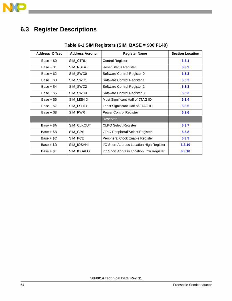
56F8014 Technical Data, Rev. 11
64 Freescale Semiconductor
6.3 Register Descriptions
Table 6-1 SIM Registers (SIM_BASE = $00 F140)
Address Offset Address Acronym Register Name Section Location
Base + $0 SIM_CTRL Control Register 6.3.1
Base + $1 SIM_RSTAT Reset Status Register 6.3.2
Base + $2 SIM_SWC0 Software Control Register 0 6.3.3
Base + $3 SIM_SWC1 Software Control Register 1 6.3.3
Base + $4 SIM_SWC2 Software Control Register 2 6.3.3
Base + $5 SIM_SWC3 Software Control Register 3 6.3.3
Base + $6 SIM_MSHID Most Significant Half of JTAG ID 6.3.4
Base + $7 SIM_LSHID Least Significant Half of JTAG ID 6.3.5
Base + $8 SIM_PWR Power Control Register 6.3.6
Reserved
Base + $A SIM_CLKOUT CLKO Select Register 6.3.7
Base + $B SIM_GPS GPIO Peripheral Select Register 6.3.8
Base + $C SIM_PCE Peripheral Clock Enable Register 6.3.9
Base + $D SIM_IOSAHI I/O Short Address Location High Register 6.3.10
Base + $E SIM_IOSALO I/O Short Address Location Low Register 6.3.10

Register Descriptions
56F8014 Technical Data, Rev. 11
Freescale Semiconductor 65
Figure 6-1 SIM Register Map Summary
6.3.1 SIM Control Register (SIM_CTRL)
Figure 6-2 SIM Control Register (SIM_CTRL)
6.3.1.1 Timer Channel 3 Stop Disable (TC3_SD)—Bit 15This bit enables the operation of the Timer Channel 3 peripheral clock in Stop mode.
• 0 = Timer Channel 3 disabled in Stop mode
Add. Offset
Address Acronym 15 14 13 12 11 10 9 8 7 6 5 4 3 2 1 0
$0 SIM_CTRL
R TC3_SD
TC2_SD
TC1_SD
TC0_SD
SCI_SD
0 TC3_INP
0 0 0 ONCE EBL0
SW RST
STOP_DISABLE
WAIT_DISABLEW
$1 SIM_RSTAT
R 0 0 0 0 0 0 0 0 0 0SWR COPR EXTR POR
0 0W
$2 SIM_SWC0R
Software Control Data 0W
$3 SIM_SWC1R
Software Control Data 1W
$4 SIM_SWC2R
Software Control Data 2W
$5 SIM_SWC3R
Software Control Data 3W
$6 SIM_MSHIDR 0 0 0 0 0 0 0 1 1 1 1 1 0 0 1 0W
$7 SIM_LSHIDR 0 1 0 0 0 0 0 0 0 0 0 1 1 1 0 1W
$8 SIM_PWRR 0 0 0 0 0 0 0 0 0 0 0 0 0 0
LRSTDBYW
Reserved
$A SIM_CLKOUT
R 0 0 0 0 0 0PWM3 PWM2 PWM1 PWM0 CLK
DIS CLKOSELW
$B SIM_GPSR
TCR PCR0 0 CFG_
B7CFG_
B6CFG_
B5CFG_
B4CFG_
B3CFG_
B2CFG_
B1CFG_
B0 CFG_A5 CFG_A4W
$C SIM_PCER
I2C0
ADC0 0 0 0 0 0
TMR0
SCI0
SPI0
PWMW
$D SIM_IOSAHIR 0 0 0 0 0 0 0 0 0 0 0 0 0 0
ISAL[23:22]W
$E SIM_IOSALOR
ISAL[21:6]W
0 = Read as 0 1 = Read as 1= Reserved = Reserved
Base + $0 15 14 13 12 11 10 9 8 7 6 5 4 3 2 1 0Read TC3_
SDTC2_SD
TC1_SD
TC0_SD
SCI_SD
0 TC3_INP
0 0 0 ONCE EBL
SW RST
STOP_DISABLE
WAIT_DISABLEWrite
RESET 0 0 0 0 0 0 0 0 0 0 0 0 0 0 0 0

56F8014 Technical Data, Rev. 11
66 Freescale Semiconductor
• 1 = Timer Channel 3 enabled in Stop mode
6.3.1.2 Timer Channel 2 Stop Disable (TC2_SD)—Bit 14This bit enables the operation of the Timer Channel 2 peripheral clock in Stop mode.
• 0 = Timer Channel 2 disabled in Stop mode• 1 = Timer Channel 2 enabled in Stop mode
6.3.1.3 Timer Channel 1 Stop Disable (TC1_SD)—Bit 13This bit enables the operation of the Timer Channel 1 peripheral clock in Stop mode.
• 0 = Timer Channel 1 disabled in Stop mode• 1 = Timer Channel 1 enabled in Stop mode
6.3.1.4 Timer Channel 0 Stop Disable (TC0_SD)—Bit 12This bit enables the operation of the Timer Channel 0 peripheral clock in Stop mode.
• 0 = Timer Channel 0 disabled in Stop mode• 1 = Timer Channel 0 enabled in Stop mode
6.3.1.5 SCI Stop Disable (SCI_SD)—Bit 11This bit enables the operation of the SCI peripheral clock in Stop mode. This is recommended for use inLIN mode so that the SCI can generate interrupts and recover from Stop mode while the LIN interface isin Sleep mode and using Stop mode to reduce power consumption.
• 0 = SCI disabled in Stop mode• 1 = SCI enabled in Stop mode
6.3.1.6 Reserved—Bit 10This bit field is reserved or not implemented. It is read as 0 and cannot be modified by writing.
6.3.1.7 Timer Channel 3 Input (TC3_INP)—Bit 9This bit selects the input of Timer Channel 3 to be from the PWM sync signal or GPIO pin.
• 1 = Timer Channel 3 Input from PWM sync signal• 0 = Timer Channel 3 Input controlled by SIM_GPS register CFG_B3 and CFG_A5 fields
6.3.1.8 Reserved—Bits 8–6This bit field is reserved or not implemented. It is read as 0 and cannot be modified by writing.
6.3.1.9 OnCE Enable (ONCEEBL)—Bit 5• 0 = OnCE clock to 56800E core enabled when core TAP is enabled• 1 = OnCE clock to 56800E core is always enabled
6.3.1.10 Software Reset (SWRST)—Bit 4Writing 1 to this field will cause the part to reset.

Register Descriptions
56F8014 Technical Data, Rev. 11
Freescale Semiconductor 67
6.3.1.11 Stop Disable (STOP_DISABLE[1:0])—Bits 3–2• 00 = Stop mode will be entered when the 56800E core executes a STOP instruction• 01 = The 56800E STOP instruction will not cause entry into Stop mode• 10 = Stop mode will be entered when the 56800E core executes a STOP instruction and the
STOP_DISABLE field is write-protected until the next reset• 11 = The 56800E STOP instruction will not cause entry into Stop mode and the STOP_DISABLE field is
write-protected until the next reset
6.3.1.12 Wait Disable (WAIT_DISABLE[1:0])—Bits 1–0• 00 = Wait mode will be entered when the 56800E core executes a WAIT instruction• 01 = The 56800E WAIT instruction will not cause entry into Wait mode• 10 = Wait mode will be entered when the 56800E core executes a WAIT instruction and the
WAIT_DISABLE field is write-protected until the next reset• 11 = The 56800E WAIT instruction will not cause entry into Wait mode and the WAIT_DISABLE field is
write-protected until the next reset
6.3.2 SIM Reset Status Register (SIM_RSTAT)This register is updated upon any system reset and indicates the cause of the most recent reset. It alsocontrols whether the COP reset vector or regular reset vector in the vector table is used. This register isasynchronously reset during Power-On Reset (see power supervisor module) and subsequently issynchronously updated based on the level of the external reset, software reset, or cop reset inputs. Onlyone source will ever be indicated. In the event that multiple reset sources assert simultaneously, thehighest-precedence source will be indicated. The precedence from highest to lowest is POR, EXTR,COPR, and SWR. While POR is always set during a Power-On Reset, EXTR will become set if theexternal reset pin is asserted or remains asserted after the Power-On Reset (POR) has deasserted.
Figure 6-3 SIM Reset Status Register (SIM_RSTAT)
6.3.2.1 Reserved—Bits 15–6This bit field is reserved or not implemented. It is read as zero and cannot be modified by writing.
6.3.2.2 Software Reset (SWR)—Bit 5When set, this bit indicates that the previous system reset occurred as a result of a software reset (written 1 to SW RST bit in the SIM_CTRL register). It will not be set if a COP, external, or POR reset also occurred.
6.3.2.3 COP Reset (COPR)—Bit 4When set, this bit indicates that the previous system reset was caused by the Computer Operating Properly
Base + $1 15 14 13 12 11 10 9 8 7 6 5 4 3 2 1 0Read 0 0 0 0 0 0 0 0 0 0
SWR COPR EXTR POR0 0
WriteRESET 0 0 0 0 0 0 0 0 0 0 0 0

56F8014 Technical Data, Rev. 11
68 Freescale Semiconductor
(COP) timer. It will not be set if an external or POR reset also occurred. If COPR is set as code startsexecuting, the COP reset vector in the vector table will be used. Otherwise, the normal reset vector is used.
6.3.2.4 External Reset (EXTR)—Bit 3When set, this bit indicates that the previous system reset was caused by an external reset. It will only beset if the external reset pin was asserted or remained asserted after the Power-On Reset deasserted.
6.3.2.5 Power-On Reset (POR)—Bit 2This bit is set during a Power-On Reset.
6.3.2.6 Reserved—Bits 1–0This bit field is reserved or not implemented. It is read as 0 and cannot be modified by writing.
6.3.3 SIM Software Control Registers (SIM_SWC0, SIM_SWC1, SIM_SWC2, and SIM_SWC3)
Only SIM_SWC0 is shown in this section. SIM_SWC1, SIM_SWC2, and SIM_SWC3 are identical infunctionality.
Figure 6-4 SIM Software Control Register 0 (SIM_SWC0)
6.3.3.1 Software Control Data 0 (FIELD)—Bits 15–0This register is reset only by the Power-On Reset (POR). It has no part-specific functionality and isintended for use by a software developer to contain data that will be unaffected by the other reset sources(RESET pin, software reset, and COP reset).
6.3.4 Most Significant Half of JTAG ID (SIM_MSHID)This read-only register displays the most significant half of the JTAG ID for the chip. This register reads$01F2.
Figure 6-5 Most Significant Half of JTAG ID (SIM_MSHID)
Base + $2 15 14 13 12 11 10 9 8 7 6 5 4 3 2 1 0Read
Software Control Data 0Write
RESET 0 0 0 0 0 0 0 0 0 0 0 0 0 0 0 0
Base + $6 15 14 13 12 11 10 9 8 7 6 5 4 3 2 1 0Read 0 0 0 0 0 0 0 1 1 1 1 1 0 0 1 0
WriteRESET 0 0 0 0 0 0 0 1 1 1 1 1 0 0 1 0

Register Descriptions
56F8014 Technical Data, Rev. 11
Freescale Semiconductor 69
6.3.5 Least Significant Half of JTAG ID (SIM_LSHID)This read-only register displays the least significant half of the JTAG ID for the chip. This register reads$401D.
Figure 6-6 Least Significant Half of JTAG ID (SIM_LSHID)
6.3.6 SIM Power Control Register (SIM_PWR)This register controls the Standby mode of the large regulator. The large regulator derives the core digitallogic power supply from the IO power supply. In some circumstances, the large regulator may be put in areduced-power Standby mode without interfering with part operation. Refer to the overview ofpower-down modes and the overview of clock generation for more information on the use of largeregulator standby.
Figure 6-7 SIM Power Control Register (SIM_PWR)
6.3.6.1 Reserved—Bits 15–2This bit field is reserved or not implemented. It is read as 0 and cannot be modified by writing.
6.3.6.2 Large Regulator Standby Mode[1:0] (LRSTDBY)—Bits 1–0This bit controls the pull-up resistors on the IRQA pin.
• 00 = Large regulator is in Normal mode• 01 = Large regulator is in Standby (reduced-power) mode• 10 = Large regulator is in Normal mode and the LRSTDBY field is write-protected until the next reset• 11 = Large regulator is in Standby mode and the LRSTDBY field is write-protected until the next reset
Note: Standby mode can be used when the device operates below 200 kHz if the PLL is shut down.
6.3.7 CLKO Select Register (SIM_CLKOUT)The CLKO select register can be used to multiplex out selected clocks generated inside the clockgeneration and SIM modules. All functionality is for test purposes only and is subject tounspecified latencies. Glitches may be produced when the clock is enabled or switched.
Base + $7 15 14 13 12 11 10 9 8 7 6 5 4 3 2 1 0Read 0 1 0 0 0 0 0 0 0 0 0 1 1 1 0 1
WriteRESET 0 1 0 0 0 0 0 0 0 0 0 1 1 1 0 1
Base + $8 15 14 13 12 11 10 9 8 7 6 5 4 3 2 1 0Read 0 0 0 0 0 0 0 0 0 0 0 0 0 0
LRSTDBYWrite
RESET 0 0 0 0 0 0 0 0 0 0 0 0 0 0 0 0

56F8014 Technical Data, Rev. 11
70 Freescale Semiconductor
The lower four bits of the GPIO A register can function as GPIO, PWM, or as additional clock outputsignals. GPIO has priority and is enabled/disabled via the GPIOA_PEREN. If GPIOA[3:0] areprogrammed to operate as peripheral outputs, then the choice between PWM and additional clock outputsis done here in the CLKOUT. The default state is for the peripheral function of GPIOA[3:0] to beprogrammed as PWM. This can be changed by altering PWM3 through PWM0.
Figure 6-8 CLKO Select Register (SIM_CLKOUT)
6.3.7.1 Reserved—Bits 15–10This bit field is reserved or not implemented. It is read as 0 and cannot be modified by writing.
6.3.7.2 PWM3—Bit 9• 0 = Peripheral output function of GPIOA[3] is defined to be PWM3• 1 = Peripheral output function of GPIOA[3] is defined to be the Relaxation Oscillator Clock
6.3.7.3 PWM2—Bit 8• 0 = Peripheral output function of GPIOA[2] is defined to be PWM2• 1 = Peripheral output function of GPIOA[2] is defined to be the system clock
6.3.7.4 PWM1—Bit 7• 0 = Peripheral output function of GPIOA[1] is defined to be PWM1• 1 = Peripheral output function of GPIOA[1] is defined to be two times the rate of the system clock
6.3.7.5 PWM0—Bit 6• 0 = Peripheral output function of GPIOA[0] is defined to be PWM0• 1 = Peripheral output function of GPIOA[0] is defined to be three times the rate of the system clock
6.3.7.6 Clockout Disable (CLKDIS)—Bit 5• 0 = CLKOUT output is enabled and will output the signal indicated by CLKOSEL• 1 = CLKOUT is 0
6.3.7.7 Clockout Select (CLKOSEL)—Bits 4–0Selects clock to be muxed out on the CLKO pin.
• 00000 = Reserved for factory test—Continuous system clock• 01001 = Reserved for factory test—OCCS MSTR OSC clock • 01011 = Reserved for factory test—ADC clock• 01100 = Reserved for factory test—JTAG TCLK
Base + $A 15 14 13 12 11 10 9 8 7 6 5 4 3 2 1 0Read 0 0 0 0 0 0 PWM
3PWM
2 PWM1 PWM0 CLKDIS CLKOSEL
WriteRESET 0 0 0 0 0 0 0 0 0 0 1 0 0 0 0 0
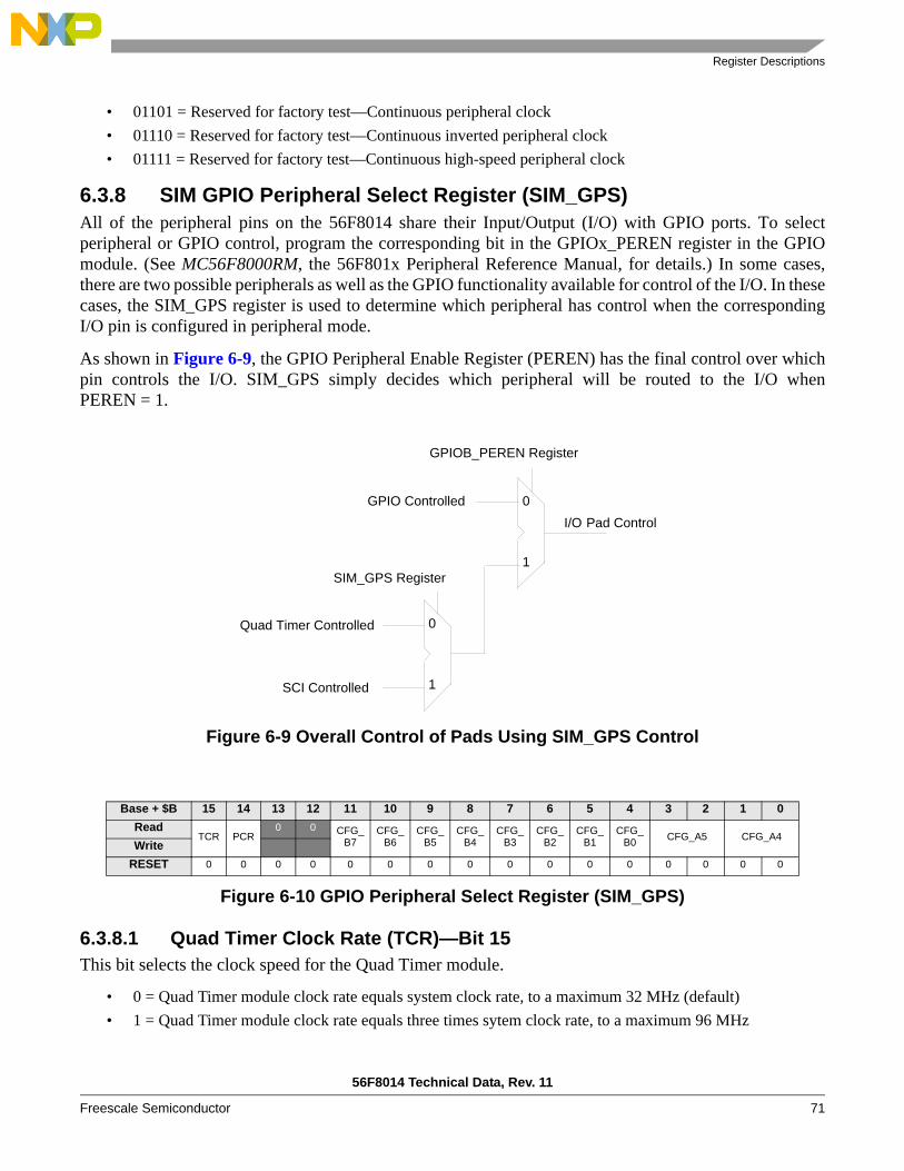
Register Descriptions
56F8014 Technical Data, Rev. 11
Freescale Semiconductor 71
• 01101 = Reserved for factory test—Continuous peripheral clock• 01110 = Reserved for factory test—Continuous inverted peripheral clock• 01111 = Reserved for factory test—Continuous high-speed peripheral clock
6.3.8 SIM GPIO Peripheral Select Register (SIM_GPS)All of the peripheral pins on the 56F8014 share their Input/Output (I/O) with GPIO ports. To selectperipheral or GPIO control, program the corresponding bit in the GPIOx_PEREN register in the GPIOmodule. (See MC56F8000RM, the 56F801x Peripheral Reference Manual, for details.) In some cases,there are two possible peripherals as well as the GPIO functionality available for control of the I/O. In thesecases, the SIM_GPS register is used to determine which peripheral has control when the correspondingI/O pin is configured in peripheral mode.
As shown in Figure 6-9, the GPIO Peripheral Enable Register (PEREN) has the final control over whichpin controls the I/O. SIM_GPS simply decides which peripheral will be routed to the I/O whenPEREN = 1.
Figure 6-9 Overall Control of Pads Using SIM_GPS Control
Figure 6-10 GPIO Peripheral Select Register (SIM_GPS)
6.3.8.1 Quad Timer Clock Rate (TCR)—Bit 15This bit selects the clock speed for the Quad Timer module.
• 0 = Quad Timer module clock rate equals system clock rate, to a maximum 32 MHz (default)• 1 = Quad Timer module clock rate equals three times sytem clock rate, to a maximum 96 MHz
Base + $B 15 14 13 12 11 10 9 8 7 6 5 4 3 2 1 0Read
TCR PCR0 0 CFG_
B7CFG_
B6CFG_
B5CFG_
B4CFG_
B3CFG_
B2CFG_
B1CFG_
B0 CFG_A5 CFG_A4Write
RESET 0 0 0 0 0 0 0 0 0 0 0 0 0 0 0 0
GPIOB_PEREN Register
GPIO ControlledI/O Pad Control
SIM_GPS Register
Quad Timer Controlled
SCI Controlled
0
1
0
1
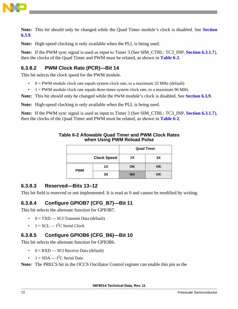
56F8014 Technical Data, Rev. 11
72 Freescale Semiconductor
Note: This bit should only be changed while the Quad Timer module’s clock is disabled. See Section6.3.9.
Note: High-speed clocking is only available when the PLL is being used.
Note: If the PWM sync signal is used as input to Timer 3 (See SIM_CTRL: TC3_INP, Section 6.3.1.7),then the clocks of the Quad Timer and PWM must be related, as shown in Table 6-2.
6.3.8.2 PWM Clock Rate (PCR)—Bit 14This bit selects the clock speed for the PWM module.
• 0 = PWM module clock rate equals system clock rate, to a maximum 32 MHz (default)• 1 = PWM module clock rate equals three times system clock rate, to a maximum 96 MHz
Note: This bit should only be changed while the PWM module’s clock is disabled. See Section 6.3.9.
Note: High-speed clocking is only available when the PLL is being used.
Note: If the PWM sync signal is used as input to Timer 3 (See SIM_CTRL: TC3_INP, Section 6.3.1.7),then the clocks of the Quad Timer and PWM must be related, as shown in Table 6-2.
6.3.8.3 Reserved—Bits 13–12This bit field is reserved or not implemented. It is read as 0 and cannot be modified by writing.
6.3.8.4 Configure GPIOB7 (CFG_B7)—Bit 11This bit selects the alternate function for GPIOB7.
• 0 = TXD — SCI Transmit Data (default)
• 1 = SCL — I2C Serial Clock
6.3.8.5 Configure GPIOB6 (CFG_B6)—Bit 10This bit selects the alternate function for GPIOB6.
• 0 = RXD — SCI Receive Data (default)
• 1 = SDA — I2C Serial DataNote: The PRECS bit in the OCCS Oscillator Control register can enable this pin as the
Table 6-2 Allowable Quad Timer and PWM Clock Rates when Using PWM Reload Pulse
Quad Timer
Clock Speed 1X 3X
PWM1X OK OK
3X NO OK

Register Descriptions
56F8014 Technical Data, Rev. 11
Freescale Semiconductor 73
source clock to the chip. In this mode, make sure that no on-chip peripheral (including the GPIO) is driving this pin.
6.3.8.6 Configure GPIOB5 (CFG_B5)—Bit 9This bit selects the alternate function for GPIOB5.
• 0 = T1 — Timer channel 1 input/output (default)• 1 = FAULT3 — PWM FAULT3 input
6.3.8.7 Configure GPIOB4 (CFG_B4)—Bit 8This bit selects the alternate function for GPIOB4.
• 0 = T0 — Timer channel 0 input/output (default)• 1 = CLKO — Clock output
6.3.8.8 Configure GPIOB3 (CFG_B3)—Bit 7This bit selects the alternate function for GPIOB3.
• 0 = MOSI — SPI master out/slave in (default)• 1 = T3 — Timer channel 3 input/output
6.3.8.9 Configure GPIOB2 (CFG_B2)—Bit 6This bit selects the alternate function for GPIOB2.
• 0 = MISO — SPI master in/slave out (default)• 1 = T2 — Timer channel 2 input/output
6.3.8.10 Configure GPIOB1 (CFG_B1)—Bit 5This bit selects the alternate function for GPIOB1.
• 0 = SS — SPI Slave Select (default)
• 1 = SDA — I2C Serial Data
6.3.8.11 Configure GPIOB0 (CFG_B0)—Bit 4This bit selects the alternate function for GPIOB0.
• 0 = SCLK — SPI Serial Clock (default)• 1 = SCL — I2C Serial Clock
6.3.8.12 Configure GPIOA5[1:0] (CFG_A5)—Bits 3–2These bits select the alternate function for GPIOA5.
• 00 = PWM5 — PWM5 output (default)• 01 = PWM5 — PWM5 output• 10 = FAULT2 — PWM FAULT2 input
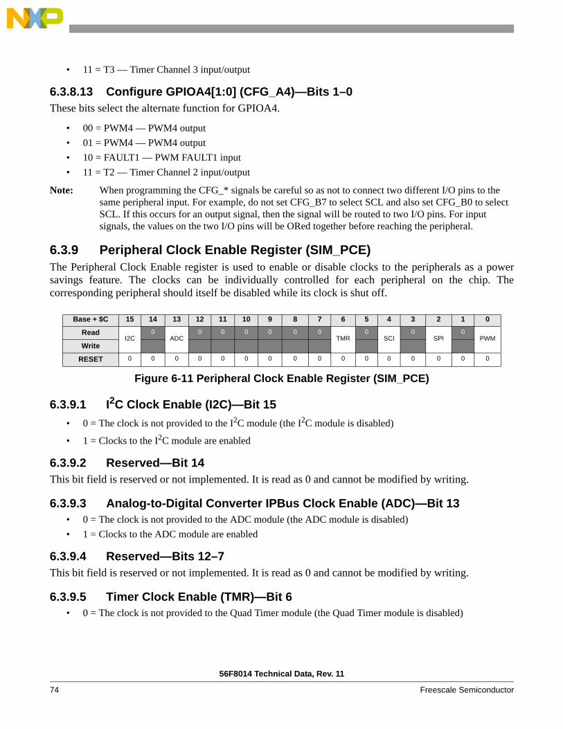
56F8014 Technical Data, Rev. 11
74 Freescale Semiconductor
• 11 = T3 — Timer Channel 3 input/output
6.3.8.13 Configure GPIOA4[1:0] (CFG_A4)—Bits 1–0These bits select the alternate function for GPIOA4.
• 00 = PWM4 — PWM4 output• 01 = PWM4 — PWM4 output• 10 = FAULT1 — PWM FAULT1 input• 11 = T2 — Timer Channel 2 input/output
Note: When programming the CFG_* signals be careful so as not to connect two different I/O pins to the same peripheral input. For example, do not set CFG_B7 to select SCL and also set CFG_B0 to select SCL. If this occurs for an output signal, then the signal will be routed to two I/O pins. For input signals, the values on the two I/O pins will be ORed together before reaching the peripheral.
6.3.9 Peripheral Clock Enable Register (SIM_PCE)The Peripheral Clock Enable register is used to enable or disable clocks to the peripherals as a powersavings feature. The clocks can be individually controlled for each peripheral on the chip. Thecorresponding peripheral should itself be disabled while its clock is shut off.
Figure 6-11 Peripheral Clock Enable Register (SIM_PCE)
6.3.9.1 I2C Clock Enable (I2C)—Bit 15• 0 = The clock is not provided to the I2C module (the I2C module is disabled)
• 1 = Clocks to the I2C module are enabled
6.3.9.2 Reserved—Bit 14This bit field is reserved or not implemented. It is read as 0 and cannot be modified by writing.
6.3.9.3 Analog-to-Digital Converter IPBus Clock Enable (ADC)—Bit 13• 0 = The clock is not provided to the ADC module (the ADC module is disabled)• 1 = Clocks to the ADC module are enabled
6.3.9.4 Reserved—Bits 12–7This bit field is reserved or not implemented. It is read as 0 and cannot be modified by writing.
6.3.9.5 Timer Clock Enable (TMR)—Bit 6• 0 = The clock is not provided to the Quad Timer module (the Quad Timer module is disabled)
Base + $C 15 14 13 12 11 10 9 8 7 6 5 4 3 2 1 0
ReadI2C
0ADC
0 0 0 0 0 0TMR
0SCI
0SPI
0PWM
Write
RESET 0 0 0 0 0 0 0 0 0 0 0 0 0 0 0 0

Register Descriptions
56F8014 Technical Data, Rev. 11
Freescale Semiconductor 75
• 1 = Clocks to the Quad Timer module are enabled
6.3.9.6 Reserved—Bit 5This bit field is reserved or not implemented. It is read as 0 and cannot be modified by writing.
6.3.9.7 SCI IPBus Clock Enable (SCI)—Bit 4• 0 = The clock is not provided to the SCI module (the SCI module is disabled)• 1 = Clocks to the SCI module are enabled
6.3.9.8 Reserved—Bit 3This bit field is reserved or not implemented. It is read as 0 and cannot be modified by writing.
6.3.9.9 SPI Clock Enable (SPI)—Bit 2• 0 = The clock is not provided to the SPI module (the SPI module is disabled)• 1 = Clocks to the SPI module are enabled
6.3.9.10 Reserved—Bit 1This bit field is reserved or not implemented. It is read as 0 and cannot be modified by writing.
6.3.9.11 PWM Clock Enable (PWM)—Bit 0• 0 = The clock is not provided to the PWM module (the PWM module is disabled)• 1 = Clocks to the PWM module are enabled
6.3.10 I/O Short Address Location Register (SIM_IOSAHI and SIM_IOSALO)
The I/O Short Address Location registers are used to specify the memory referenced via the I/O shortaddress mode. The I/O short address mode allows the instruction to specify the lower six bits of address;the upper address bits are not directly controllable. This register set allows limited control of the fulladdress, as shown in Figure 6-12.

56F8014 Technical Data, Rev. 11
76 Freescale Semiconductor
Figure 6-12 I/O Short Address Determination
With this register set, an interrupt driver can set the SIM_IOSALO register pair to point to its peripheralregisters and then use the I/O Short addressing mode to reference them. The ISR should restore this registerto its previous contents prior to returning from interrupt.
Note: The default value of this register set points to the EOnCE registers.
Note: The pipeline delay between setting this register set and using short I/O addressing with the new value is five instruction cycles.
Figure 6-13 I/O Short Address Location High Register (SIM_IOSAHI)
6.3.10.1 Reserved—Bits 15—2This bit field is reserved or not implemented. It is read as 0 and cannot be modified by writing.
6.3.10.2 Input/Output Short Address Location (ISAL[23:22])—Bit 1–0This field represents the upper two address bits of the “hard coded” I/O short address.
Base + $D 15 14 13 12 11 10 9 8 7 6 5 4 3 2 1 0
Read 0 0 0 0 0 0 0 0 0 0 0 0 0 0ISAL[23:22]
Write
RESET 0 0 0 0 0 0 0 0 0 0 0 0 0 0 1 1
Instruction Portion“Hard Coded” Address Portion
6 Bits from I/O Short Address Mode Instruction
16 Bits from SIM_IOSALO Register
2 bits from SIM_IOSAHI Register
Full 24-Bit for Short I/O Address
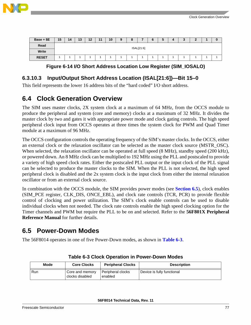
Clock Generation Overview
56F8014 Technical Data, Rev. 11
Freescale Semiconductor 77
Figure 6-14 I/O Short Address Location Low Register (SIM_IOSALO)
6.3.10.3 Input/Output Short Address Location (ISAL[21:6])—Bit 15–0This field represents the lower 16 address bits of the “hard coded” I/O short address.
6.4 Clock Generation OverviewThe SIM uses master clocks, 2X system clock at a maximum of 64 MHz, from the OCCS module toproduce the peripheral and system (core and memory) clocks at a maximum of 32 MHz. It divides themaster clock by two and gates it with appropriate power mode and clock gating controls. The high speedperipheral clock input from OCCS operates at three times the system clock for PWM and Quad Timermodule at a maximum of 96 MHz.
The OCCS configuration controls the operating frequency of the SIM’s master clocks. In the OCCS, eitheran external clock or the relaxation oscillator can be selected as the master clock source (MSTR_OSC).When selected, the relaxation oscillator can be operated at full speed (8 MHz), standby speed (200 kHz),or powered down. An 8 MHz clock can be multiplied to 192 MHz using the PLL and postscaled to providea variety of high speed clock rates. Either the postscaled PLL output or the input clock of the PLL signalcan be selected to produce the master clocks to the SIM. When the PLL is not selected, the high speedperipheral clock is disabled and the 2x system clock is the input clock from either the internal relaxationoscillator or from an external clock source.
In combination with the OCCS module, the SIM provides power modes (see Section 6.5), clock enables(SIM_PCE register, CLK_DIS, ONCE_EBL), and clock rate controls (TCR, PCR) to provide flexiblecontrol of clocking and power utilization. The SIM’s clock enable controls can be used to disableindividual clocks when not needed. The clock rate controls enable the high speed clocking option for theTimer channels and PWM but require the PLL to be on and selected. Refer to the 56F801X PeripheralReference Manual for further details.
6.5 Power-Down ModesThe 56F8014 operates in one of five Power-Down modes, as shown in Table 6-3.
Base + $E 15 14 13 12 11 10 9 8 7 6 5 4 3 2 1 0
Read ISAL[21:6]
Write
RESET 1 1 1 1 1 1 1 1 1 1 1 1 1 1 1 1
Table 6-3 Clock Operation in Power-Down ModesMode Core Clocks Peripheral Clocks Description
Run Core and memory clocks disabled
Peripheral clocks enabled
Device is fully functional

56F8014 Technical Data, Rev. 11
78 Freescale Semiconductor
The power modes provide additional means to disable clock domains, configure the voltage regulator, andconfigure clock generation to manage power utilization, as shown in Table 6-3. Run, Wait, and Stopmodes provide means of enabling/disabling the peripheral and/or core clocking as a group. Stop disablecontrols are provided for selected peripherals in the control register so that these peripheral clocks canoptionally continue to operate in Stop mode and generate interrupts which will return the part from Stopto Run mode. Standby mode provides normal operation but at very low speed and power utilization. It ispossible to invoke Stop or Wait mode while in Standby mode for even greater levels of power reduction.A 200 kHz clock external clock can optionally be used in Standby mode to produce the required Standby100 kHz system bus rate. Power-down mode, which selects the ROSC clock source but shuts it off, fullydisables the part and minimizes its power utilization but is only recoverable via reset.
When the PLL is not selected and the system bus is operating at around 100 kHz, the large regulator can
Wait Core and memory clocks disabled
Peripheral clocks enabled
Core executes WAIT instruction to enter this mode. Typically used for power-conscious applications.Possible recoveries from Wait mode to Run mode are:1. Any interrupt2. Executing a Debug mode entry command during the 56800E core JTAG interface2. Any reset (POR, external, software, COP)
Stop Master clock generation in the OCCS remains operational, but the SIM disables the generation of system and peripheral clocks.
Core executes STOP instruction to enter this mode. Possible recoveries from Stop mode to Run mode are:1. Interrupt from Timer channels that have been configured to operate in Stop mode (TCx_SD)2. Interrupt for SCI configured to operate in Stop mode (SCI_SD)3. Low-voltage interrupt4. Executing a Debug mode entry command using the 56800E core JTAG interface5. Any reset (POR, external, software, COP)
Standby The OCCS generates the 2x System Clock at a reduced frequency (200 kHz). The PLL and high speed peripheral clocks are disabled and the high-speed peripheral option is not available. System and peripheral clocks operate at 100 kHz.
The user configures the OCCS and SIM to select the relaxation oscillator clock source (PRECS), shut down the PLL (PLLPD), put the relaxation oscillator in Standby mode (ROSB), and put the large regulator in Standby (LRSTDBY). The part is fully operational, but operating at a minimum frequency and power configuration. Recovery requires reversing the sequence used to enter this mode (allowing for PLL lock time).
Power-Down Master clock generation in the OCCS is completely shut down. All system and peripheral clocks are disabled.
The user configures the OCCS and SIM to enter Standby mode as shown in the previous description, followed by powering down the oscillator (ROPD). The only possible recoveries from this mode are:1. External reset2. Power-on reset
Table 6-3 Clock Operation in Power-Down Modes (Continued)Mode Core Clocks Peripheral Clocks Description

Resets
56F8014 Technical Data, Rev. 11
Freescale Semiconductor 79
be put into its Standby mode (LRSTDBY) to reduce the power utilization of that regulator.
All peripherals, except the COP/watchdog timer, run at the system clock (peripheral bus) frequency1,which is the same as the main processor frequency in this architecture. The COP timer runs atMSTR_OSC / 1024. The maximum frequency of operation is SYS_CLK = 32MHz. The only exception isthe Quad Timer and PWM, which can be configured to operate at three times the system bus rate usingTCR and PCR controls, provided the PLL is active and selected.
6.6 Resets The SIM supports four sources of reset, as shown in Figure 6-15. The two asynchronous sources are theexternal reset pin and the Power-On Reset (POR). The two synchronous sources are the software reset,which is generated within the SIM itself by writing the SIM_CTRL register in Section 6.3.1, and the COPreset. The SIM uses these to generate resets for the internal logic. These are outlined in Table 6-4. Thefirst column lists the four primary resets which are calculated. The JTAG circuitry is reset by the Power-OnReset. Columns two through five indicate which reset sources trigger these reset signals. The last columnprovides additional detail.
Figure 6-15 provides a graphic illustration of the details in Table 6-4. Note that the POR_Delay blocksuse the Relaxation Oscillator Clock as their time base since other system clocks are inactive during thisphase of reset.
1. The Quad Timer and PWM modules can be operated at three times the IPBus clock frequency.
Table 6-4 Primary System Resets
Reset Sources
Reset Signal POR External Software COP Comments
EXTENDED_POR X Stretched version of POR. Relevant 64 Relaxation Oscillator Clock cycles after POR deasserts.
CLKGEN_RST X X X X Released 32 Relaxation Oscillator Clock cycles after all reset sources have released.
PERIP_RST X X X X Releases 32 Relaxation Oscillator Clock cycles after the CLKGEN_RST is released.
CORE_RST X X X X Releases 32 SYS_CLK periods after PERIP_RST is released.

56F8014 Technical Data, Rev. 11
80 Freescale Semiconductor
Figure 6-15 Sources of RESET Functional Diagram (Test modes not included)
POR resets are extended 64 MSTR_OSC clocks to stabilize the power supply. All resets are subsequentlyextended for an additional 32 MSTR_OSC clocks and 64 system clocks as the various internal resetcontrols are released. Given the normal relaxation oscillator rate of 8MHz, the duration of a POR resetfrom when power comes on to when code is running is 28μS. An external reset generation chip may alsobe used. Resets may be asserted asynchronously, but they are always released internally on a rising edgeof the system clock.
EXTENDED_PORJTAG
MemorySubsystem
Peripherals
56800E
CORE_RST
Delay 32sys clocks
OCCSCLKGEN_RST
PERIP_RST
Delay 32sys clocks
pulse shaper
pulse shaper
SW Reset
pulse shaper
Delay 32MSTR_OSC
Clocks
pulse shaper
PORPower-On
Reset(active
low)
External RESET IN
(active low)
COP(active
low)
RESET
Delay 64MSTR_OSC
Clocks
Delay blocks assert immediately and deassert only after the programmed number of clock cycles.
COMBINED_RST

Clocks
56F8014 Technical Data, Rev. 11
Freescale Semiconductor 81
6.7 ClocksThe memory, peripheral and core clocks all operate at the same frequency (32MHz max) with theexception of the TMR and PWM peripheral clocks, which have the option (using TCR and PCR) to operatethree times faster. The SIM is responsible for stalling individual clocks as a response to various hold-offrequests, low power modes, and other configuration parameters. The SIM has access to the followingsignals from the OCCS module:
While the SIM generates the ADC peripheral clock in the same way it generates all other peripheral clocks,the ADC standby and conversion clocks are generated by a direct interface between the ADC and theOCCS module.
Figure 6-16 illustrates clock relationships to one another and to the various resets as the device comes outof reset. RST is assumed to be the logical AND of all active-low system resets (for example, POR, externalreset, COP and Software reset). In the 56F8014 architecture, this signal will be stretched by the SIM for aperiod of time (up to 96 MSTR_OSC clock cycles, depending upon the status of the POR) to create theclock generation reset signal (CLKGEN_RST). The SIM should deassert CLKGEN_RST synchronouslywith the negative edge of OSC_CLK in order to avoid skew problems. CLKGEN_RST is delayed 32SYS_CLK cycles to create the peripheral reset signal (PERIP_RST). PERIP_RST is then delayed by 32SYS_CLK cycles to create CORE_RST. Both PERIP_RST and CORE_RST should be released on thenegative edge of SYS_CLK_D as shown. This phased releasing of system resets is necessary to give someperipherals (for example, the Flash interface unit) set-up time prior to the 56800E core becoming active.
MSTR_OSC This comes from the input clock source mux of the OCCS. It is the output of the relaxation oscillator or the external clock source, depending on PRECS. It is not guaranteed to be at 50% duty cycle (+ or - 10% can probably be assumed for design purposes). This clock runs continuously, even during reset and is used for reset generation.
HS_PERF The PLL multiplies the MSTR_OSC by 24, to a maximum of 192MHz. The ZSRC field in OCCS selects the active source to be the PLL. This is divided by 2 and postscaled to produce this maximum 96MHz clock. It is used without further division to produce the high-speed (3x system bus rate) variants of the Quad Timer and PWM peripheral clocks. This clock is disabled when ZSRC is selecting MSTR_OSC.
SYS_CLK_x2 The PLL can multiply the MSTR_OSC by 24, to a maximum of 192MHz. When the PLL is selected by the OCCS ZSRC field, the PLL is divided by three and postscaled to produce this maximum 64MHz clock. When MSTR_OSC is selected by the OCCS ZSRC field, MSTR_OSC feeds SYS_CLK_x2 directly. The SIM takes this clock and divides it by two to generate all the normal (1x system bus rate) peripheral and system clocks.

56F8014 Technical Data, Rev. 11
82 Freescale Semiconductor
Figure 6-16 Timing Relationships of Reset Signal to Clocks
6.8 InterruptsThe SIM generates no interrupts.
Part 7 Security FeaturesThe 56F8014 offers security features intended to prevent unauthorized users from reading the contents ofthe flash memory (FM) array. The 56F8014’s flash security consists of several hardware interlocks thatprevent unauthorized users from gaining access to the flash array.
After flash security is set, an authorized user is still able to access on-chip memory if the user purposelyincludes a subroutine to read and transfer the contents of internal memory via serial communicationperipherals, as this code would defeat the purpose of security.
7.1 Operation with Security EnabledAfter the user has programmed the flash with his application code, the 56F8014 can be secured byprogramming a security word ($E70A) into program memory location $00 1FF7. This nonvolatile wordwill keep the device secured through reset and through power-down of the device. Refer to the flash
RST
MSTR_OSC
CKGEN_RST
SYS_CLK_x2
SYS_CLK
SYS_CLK_D
SYS_CLK_DIV2
PERIP_RST
CORE_RST
Switch on falling OSC_CLK96 MSTR_OSC cycles
Switch on falling SYS_CLK
32 SYS_CLK cycles delay
32 SYS_CLK cycles delay
Maximum Delay = 64 MSTR_OSC cycles for POR reset extension and 32 MSTR_OSC cycles for combined reset extension
Switch on falling SYS_CLK

Flash Access Lock and Unlock Mechanisms
56F8014 Technical Data, Rev. 11
Freescale Semiconductor 83
memory chapter in MC56F8000RM, the 56F8000 Peripheral Reference Manual for details. When flashsecurity mode is enabled, the 56F8014 will disable the core EOnCE debug capabilities. Normal programexecution is otherwise unaffected.
7.2 Flash Access Lock and Unlock MechanismsThere are several methods that effectively lock or unlock the on-chip flash.
7.2.1 Disabling EOnCE AccessOn-chip flash can be read by issuing commands across the EOnCE port, which is the debug interface forthe 56800E CPU. The TCK, TMS, TDO, and TDI pins comprise a JTAG interface onto which the EOnCEport functionality is mapped. When the device boots, the chip-level JTAG TAP (Test Access Port) is activeand provides the chip’s boundary scan capability and access to the ID register, but proper implementationof flash security will block any attempt to access the internal flash memory via the EOnCE port whensecurity is enabled.
7.2.2 Flash Lockout Recovery Using JTAGIf the device is secured, one lockout recovery mechanism is the complete erasure of the internal flashcontents, including the configuration field, thus disabling security (the protection register is cleared). Thisdoes not compromise security, as the entire contents of the user’s secured code stored in flash are erasedbefore security is disabled on the device on the next reset or power-up sequence.
To start the lockout recovery sequence via JTAG, the JTAG public instruction(LOCKOUT_RECOVERY) must first be shifted into the chip-level TAP controller’s instruction register.Once the LOCKOUT_RECOVERY instruction has been shifted into the instruction register, the clockdivider value must be shifted into the corresponding 7-bit data register. After the data register has beenupdated, the user must transition the TAP controller into the RUN-TEST/IDLE state for the lockoutsequence to commence. The controller must remain in this state until the erase sequence has completed.Refer to MC56F8000RM, the 56F8000 Peripheral Reference Manual, for more details, or contactFreescale.
Note: Once the lockout recovery sequence has completed, the user must reset both the JTAG TAP controller and the device to return to normal unsecured operation. Power-on reset will also reset both.
7.2.3 Flash Lockout Recovery Using CodeWarriorCodeWarrior can unlock a device by selecting the Debug menu, then selecting DSP56800E, followed byUnlock Flash. Another mechanism is also built into CodeWarrior using the device’s memory configurationfile. The command Unlock_Flash_on_Connect1 in the .cfg file accomplishes the same task as using theDebug menu.
This lockout recovery mechanism also includes the complete erasure of the internal flash contents,including the configuration field, thus disabling security (the protection register is cleared).
7.2.4 Flash Lockout Recovery Without Mass EraseThe user can un-secure a secured device by programming the word $0000 into program memory location$00 1FF7. After completing the programming, both the JTAG TAP controller and the device must be reset

56F8014 Technical Data, Rev. 11
84 Freescale Semiconductor
in order to return to normal unsecured operation. Power-on reset will also reset both.
The user is responsible for directing the device to invoke the flash programming subroutine to reprogramthe word $0000 into program memory location $00 1FF7. This is done by, for example, toggling a specificpin, or by downloading a user-defined key through serial interfaces.
Note: Flash contents can only be programmed for 1s to 0s.
7.3 Product AnalysisThe recommended method of unsecuring a secured device for product analysis of field failures is via themethod suggested in section 7.2.4. The customer would need to supply Technical Support with the detailsof the protocol to access the subroutines in flash. An alternative method for performing analysis on asecured device would be to mass-erase and reprogram the flash with the original code, but also eithermodify the security word or else not program the security word.
Part 8 General Purpose Input/Output (GPIO)
8.1 IntroductionThis section is intended to supplement the GPIO information found in the 56F801X Peripheral ReferenceManual and contains only chip-specific information. This information supercedes the generic informationin the 56F801X Peripheral Reference Manual.
8.2 ConfigurationThere are four GPIO ports defined on the 56F8014. The width of each port, the associated peripheral andreset functions are shown in Table 8-1. The specific mapping of GPIO port pins is shown in Table 8-2.
Table 8-1 GPIO Ports Configuration
GPIO PortAvailable Pins in
56F8014Peripheral Function Reset Function
A 6 PWM, Reset GPIO, except GPIOA7
B 8 SPI, SCI, Timer GPIO
C 8 ADC Analog
D 4 JTAG JTAG

Configuration
56F8014 Technical Data, Rev. 11
Freescale Semiconductor 85
Table 8-2 GPIO External Signals MapPins in shaded rows are not available in 56F8014
GPIO Function Peripheral Function LQFPPackage Pin Notes
GPIOA0 PWM0 28 Defaults to A0
GPIOA1 PWM1 27 Defaults toA1
GPIOA2 PWM2 23 Defaults to A2
GPIOA3 PWM3 Not bonded out in 56F8014Defaults to A3
GPIOA4 PWM4 / FAULT1 / T2 22 SIM register SIM_GPS is used to select between PWM4, FAULT1, and T2Defaults to A4
GPIOA5 PWM5 / FAULT2 / T3 20 SIM register SIM_GPS is used to select between PWM5, FAULT2, and T3Defaults to A5
GPIOA6 FAULT0 Not bonded out in 56F8014Defaults to A6
GPIOA7 RESET 16 Defaults to RESET
GPIOB0 SCLK / SCL 21 SIM register SIM_GPS is used to select between SCLK and SCL Defaults to B0
GPIOB1 SS / SDA 1 SIM register SIM_GPS is used to select between SS and SDADefaults to B1
GPIOB2 MISO / T2 18 SIM register SIM_GPS is used to select between MISO and T2Defaults to B2
GPIOB3 MOSI / T3 17 SIM register SIM_GPS is used to select between MOSI and T3Defaults to B3
GPIOB4 T0 / CLKO 19 SIM register SIM_GPS is used to select between T0 and CLKODefaults to B4
GPIOB5 T1 / FAULT3 3 SIM register SIM_GPS is used to select between T1 and FAULT3 Defaults to B5

56F8014 Technical Data, Rev. 11
86 Freescale Semiconductor
8.3 Reset ValuesTables 4-16 through 4-19 detail registers for the 56F8014; Figures 8-1 through 8-4 summarize registermaps and reset values.
GPIOB6 RXD / SDA / CLKIN 32 SIM register SIM_GPS is used to select between RXD and SDA. CLKIN functionality is enabled using the PLL Control Register within the OCCS block.Defaults to B6
GPIOB7 TXD / SCL 2 SIM register SIM_GPS is used to select between TXD and SCL Defaults to B7
GPIOC0 ANA0 13 Defaults to ANA0
GPIOC1 ANA1 12 Defaults to ANA1
GPIOC2 ANA2 / VREFH 11 Defaults to ANA2
GPIOC3 ANA3 10 Defaults to ANA3
GPIOC4 ANB0 4 Defaults to ANB0
GPIOC5 ANB1 5 Defaults to ANB1
GPIOC6 ANB2 / VREFL 6 Defaults to ANB2
GPIOC7 ANB3 7 Defaults to ANB3
GPIOD0 TDI 29 Defaults to TDI
GPIOD1 TDO 31 Defaults to TDO
GPIOD2 TCK 15 Defaults to TCK
GPIOD3 TMS 30 Defaults to TMS
Table 8-2 GPIO External Signals Map (Continued)Pins in shaded rows are not available in 56F8014
GPIO Function Peripheral Function LQFPPackage Pin Notes

Reset Values
56F8014 Technical Data, Rev. 11
Freescale Semiconductor 87
Figure 8-1 GPIOA Register Map Summary
Add. Offset Register Acronym 15 14 13 12 11 10 9 8 7 6 5 4 3 2 1 0
$0 GPIOA_PUPENR 0 0 0 0 0 0 0 0
PUWRS 0 0 0 0 0 0 0 0 1 1 1 1 1 1 1 1
$1 GPIOA_DATAR 0 0 0 0 0 0 0 0
DWRS 0 0 0 0 0 0 0 0 0 1 1 1 1 1 1 1
$2 GPIOA_DDIRR 0 0 0 0 0 0 0 0
DDWRS 0 0 0 0 0 0 0 0 0 0 0 0 0 0 0 0
$3 GPIOA_PERENR 0 0 0 0 0 0 0 0
PEWRS 0 0 0 0 0 0 0 0 1 0 0 0 0 0 0 0
$4 GPIOA_IASSRTR 0 0 0 0 0 0 0 0
IAWRS 0 0 0 0 0 0 0 0 0 0 0 0 0 0 0 0
$5 GPIOA_IENR 0 0 0 0 0 0 0 0
IENWRS 0 0 0 0 0 0 0 0 0 0 0 0 0 0 0 0
$6 GPIOA_IEPOLR 0 0 0 0 0 0 0 0
IEPOLWRS 0 0 0 0 0 0 0 0 0 0 0 0 0 0 0 0
$7 GPIOA_IPENDR 0 0 0 0 0 0 0 0
IPRWRS 0 0 0 0 0 0 0 0 0 0 0 0 0 0 0 0
$8 GPIOA_IEDGER 0 0 0 0 0 0 0 0
IESWRS 0 0 0 0 0 0 0 0 0 0 0 0 0 0 0 0
$9 GPIOA_PPOUTMR 0 0 0 0 0 0 0 0
OENWRS 0 0 0 0 0 0 0 0 1 1 1 1 1 1 1 1
$A GPIOA_RDATAR 0 0 0 0 0 0 0 0 RAW DATAWRS X X X X X X X X X X X X X X X X
$B GPIOA_DRIVER 0 0 0 0 0 0 0 0
DRIVEWRS 0 0 0 0 0 0 0 0 0 0 0 0 0 0 0 0
R 0 Read as 0W ReservedRS Reset

56F8014 Technical Data, Rev. 11
88 Freescale Semiconductor
Figure 8-2 GPIOB Register Map Summary
Add. Offset Register Acronym 15 14 13 12 11 10 9 8 7 6 5 4 3 2 1 0
$0 GPIOB_PUPENR 0 0 0 0 0 0 0 0
PUWRS 0 0 0 0 0 0 0 0 1 1 1 1 1 1 1 1
$1 GPIOB_DATAR 0 0 0 0 0 0 0 0
DWRS 0 0 0 0 0 0 0 0 1 1 1 1 1 1 1 1
$2 GPIOB_DDIRR 0 0 0 0 0 0 0 0
DDWRS 0 0 0 0 0 0 0 0 0 0 0 0 0 0 0 0
$3 GPIOB_PERENR 0 0 0 0 0 0 0 0
PEWRS 0 0 0 0 0 0 0 0 0 0 0 0 0 0 0 0
$4 GPIOB_IASSRTR 0 0 0 0 0 0 0 0
IAWRS 0 0 0 0 0 0 0 0 0 0 0 0 0 0 0 0
$5 GPIOB_IENR 0 0 0 0 0 0 0 0
IENWRS 0 0 0 0 0 0 0 0 0 0 0 0 0 0 0 0
$6 GPIOB_IEPOLR 0 0 0 0 0 0 0 0
IEPOLWRS 0 0 0 0 0 0 0 0 0 0 0 0 0 0 0 0
$7 GPIOB_IPENDR 0 0 0 0 0 0 0 0
IPRWRS 0 0 0 0 0 0 0 0 0 0 0 0 0 0 0 0
$8 GPIOB_IEDGER 0 0 0 0 0 0 0 0
IESWRS 0 0 0 0 0 0 0 0 0 0 0 0 0 0 0 0
$9 GPIOB_PPOUTMR 0 0 0 0 0 0 0 0
OENWRS 0 0 0 0 0 0 0 0 1 1 1 1 1 1 1 1
$A GPIOB_RDATAR 0 0 0 0 0 0 0 0 RAW DATAWRS X X X X X X X X X X X X X X X X
$B GPIOB_DRIVER 0 0 0 0 0 0 0 0
DRIVEWRS 0 0 0 0 0 0 0 0 0 0 0 0 0 0 0 0
R 0 Read as 0W ReservedRS Reset

Reset Values
56F8014 Technical Data, Rev. 11
Freescale Semiconductor 89
Figure 8-3 GPIOC Register Map Summary
Add. Offset Register Acronym 15 14 13 12 11 10 9 8 7 6 5 4 3 2 1 0
$0 GPIOC_PUPENR 0 0 0 0 0 0 0 0
PUWRS 0 0 0 0 0 0 0 0 1 1 1 1 1 1 1 1
$1 GPIOC_DATAR 0 0 0 0 0 0 0 0
DWRS 0 0 0 0 0 0 0 0 0 0 0 0 0 0 0 0
$2 GPIOC_DDIRR 0 0 0 0 0 0 0 0
DDWRS 0 0 0 0 0 0 0 0 0 0 0 0 0 0 0 0
$3 GPIOC_PERENR 0 0 0 0 0 0 0 0
PEWRS 0 0 0 0 0 0 0 0 1 1 1 1 1 1 1 1
$4 GPIOC_IASSRTR 0 0 0 0 0 0 0 0
IAWRS 0 0 0 0 0 0 0 0 0 0 0 0 0 0 0 0
$5 GPIOC_IENR 0 0 0 0 0 0 0 0
IENWRS 0 0 0 0 0 0 0 0 0 0 0 0 0 0 0 0
$6 GPIOC_IEPOLR 0 0 0 0 0 0 0 0
IEPOLWRS 0 0 0 0 0 0 0 0 0 0 0 0 0 0 0 0
$7 GPIOC_IPENDR 0 0 0 0 0 0 0 0
IPRWRS 0 0 0 0 0 0 0 0 0 0 0 0 0 0 0 0
$8 GPIOC_IEDGER 0 0 0 0 0 0 0 0
IESWRS 0 0 0 0 0 0 0 0 0 0 0 0 0 0 0 0
$9 GPIOC_PPOUTMR 0 0 0 0 0 0 0 0
OENWRS 0 0 0 0 0 0 0 0 1 1 1 1 1 1 1 1
$A GPIOC_RDATAR 0 0 0 0 0 0 0 0 RAW DATAWRS X X X X X X X X X X X X X X X X
$B GPIOC_DRIVER 0 0 0 0 0 0 0 0
DRIVEWRS 0 0 0 0 0 0 0 0 0 0 0 0 0 0 0 0
R 0 Read as 0W ReservedRS Reset

56F8014 Technical Data, Rev. 11
90 Freescale Semiconductor
Add. Offset Register Acronym 15 14 13 12 11 10 9 8 7 6 5 4 3 2 1 0
$0 GPIOD_PUPENR 0 0 0 0 0 0 0 0 0 0 0 0
PUWRS 0 0 0 0 0 0 0 0 0 0 0 0 1 1 1 1
$1 GPIOD_DATAR 0 0 0 0 0 0 0 0 0 0 0 0 DWRS 0 0 0 0 0 0 0 0 0 0 0 0 0 0 0 0
$2 GPIOD_DDIRR 0 0 0 0 0 0 0 0 0 0 0 0
DDWRS 0 0 0 0 0 0 0 0 0 0 0 0 0 0 0 0
$3 GPIOD_PERENR 0 0 0 0 0 0 0 0 0 0 0 0
PEWRS 0 0 0 0 0 0 0 0 0 0 0 0 1 1 1 1
$4 GPIOD_IASSRTR 0 0 0 0 0 0 0 0 0 0 0 0
IAWRS 0 0 0 0 0 0 0 0 0 0 0 0 0 0 0 0
$5 GPIOD_IENR 0 0 0 0 0 0 0 0 0 0 0 0 IENWRS 0 0 0 0 0 0 0 0 0 0 0 0 0 0 0 0
$6 GPIOD_IEPOLR 0 0 0 0 0 0 0 0 0 0 0 0 IEPOLWRS 0 0 0 0 0 0 0 0 0 0 0 0 0 0 0 0
$7 GPIOD_IPENDR 0 0 0 0 0 0 0 0 0 0 0 0
IPRWRS 0 0 0 0 0 0 0 0 0 0 0 0 0 0 0 0
$8 GPIOD_IEDGER 0 0 0 0 0 0 0 0 0 0 0 0
IESWRS 0 0 0 0 0 0 0 0 0 0 0 0 0 0 0 0
$9 GPIOD_PPOUTMR 0 0 0 0 0 0 0 0 0 0 0 0
OENWRS 0 0 0 0 0 0 0 0 0 0 0 0 1 1 1 1
$A GPIOD_RDATAR 0 0 0 0 0 0 0 0 0 0 0 0 RAW DATAWRS X X X X X X X X X X X X X X X X
$B GPIOD_DRIVER 0 0 0 0 0 0 0 0 0 0 0 0
DRIVEWRS 0 0 0 0 0 0 0 0 0 0 0 0 0 0 0 0
R 0 Read as 0W Reserved

56F8014 Information
56F8014 Technical Data, Rev. 11
Freescale Semiconductor 91
Figure 8-4 GPIOD Register Map Summary
Part 9 Joint Test Action Group (JTAG)
9.1 56F8014 InformationPlease contact your Freescale sales representative or authorized distributor for device/package-specificBSDL information.
The TRST pin is not available in this package. The pin is tied to VDD in the package.
The JTAG state machine is reset during POR and can also be reset via a soft reset by holding TMS highfor five rising edges of TCK, as described in the 56F8000 Peripheral User Manual.
Part 10 Specifications
10.1 General CharacteristicsThe 56F8014 is fabricated in high-density CMOS with 5V-tolerant TTL-compatible digital inputs. Theterm “5V-tolerant” refers to the capability of an I/O pin, built on a 3.3V-compatible process technology,to withstand a voltage up to 5.5V without damaging the device. Many systems have a mixture of devicesdesigned for 3.3V and 5V power supplies. In such systems, a bus may carry both 3.3V- and 5V-compatibleI/O voltage levels (a standard 3.3V I/O is designed to receive a maximum voltage of 3.3V ± 10% duringnormal operation without causing damage). This 5V-tolerant capability therefore offers the power savingsof 3.3V I/O levels, combined with the ability to receive 5V levels without damage.
Absolute maximum ratings in Table 10-1 are stress ratings only, and functional operation at the maximumis not guaranteed. Stress beyond these ratings may affect device reliability or cause permanent damage tothe device.
Unless otherwise stated, all specifications within this chapter apply over the temperature range of -40ºC to 125ºC ambient temperature over the following supply ranges: VSS = VSSA = 0V, VDD = VDDA = 3.0–3.6V, CL < 50pF, fOP = 32MHz
RS Reset

56F8014 Technical Data, Rev. 11
92 Freescale Semiconductor
CAUTION
This device contains protective circuitry to guardagainst damage due to high static voltage or electricalfields. However, normal precautions are advised toavoid application of any voltages higher thanmaximum-rated voltages to this high-impedance circuit.Reliability of operation is enhanced if unused inputs aretied to an appropriate voltage level.
Table 10-1 Absolute Maximum Ratings (VSS = 0V, VSSA = 0V)
Characteristic Symbol Notes Min Max Unit
Supply Voltage Range VDD -0.3 4.0 V
Analog Supply Voltage Range VDDA - 0.3 4.0 V
ADC High Voltage Reference VREFH - 0.3 4.0 V
Voltage difference VDD_IO to VDDA ΔVDD - 0.3 0.3 V
Voltage difference VSS_IO to VSSA ΔVSS - 0.3 0.3 V
Input Voltage Range (Digital inputs) VIN Pin Groups 1, 2 - 0.3 6.0 V
Input Voltage Range (ADC inputs)1 VINA Pin Group 3 - 0.3 4.0 V
Input clamp current, per pin (VIN < 0)2 VIC - -20 mA
Output clamp current, per pin (VO < 0)2 VOC - -20 mA
Output Voltage Range (Normal Push-Pull mode)
VOUT Pin Group 1 -0.3 4.0 V
Output Voltage Range (Open Drain mode)
VOUTOD Pin Groups 1, 2 -0.3 6.0 V
Ambient Temperature (Automotive) TA -40 125 °C
Ambient Temperature (Industrial) TA -40 105 °C
Junction Temperature (Automotive) TJ -40 150 °C
Junction Temperature (Industrial) TJ -40 125 °C
Storage Temperature (Automotive) TSTG -55 150 °C
Storage Temperature (Industrial) TSTG -55 150 °C
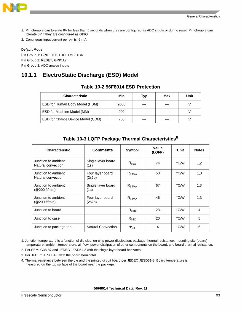
General Characteristics
56F8014 Technical Data, Rev. 11
Freescale Semiconductor 93
Default ModePin Group 1: GPIO, TDI, TDO, TMS, TCK Pin Group 2: RESET, GPIOA7 Pin Group 3: ADC analog inputs
10.1.1 ElectroStatic Discharge (ESD) Model
1. Junction temperature is a function of die size, on-chip power dissipation, package thermal resistance, mounting site (board) temperature, ambient temperature, air flow, power dissipation of other components on the board, and board thermal resistance.
2. Per SEMI G38-87 and JEDEC JESD51-2 with the single layer board horizontal.3. Per JEDEC JESC51-6 with the board horizontal.4. Thermal resistance between the die and the printed circuit board per JEDEC JESD51-8. Board temperature is
measured on the top surface of the board near the package.
1. Pin Group 3 can tolerate 6V for less than 5 seconds when they are configured as ADC inputs or during reset. Pin Group 3 cantolerate 6V if they are configured as GPIO.
2. Continuous input current per pin is -2 mA
Table 10-2 56F8014 ESD Protection
Characteristic Min Typ Max Unit
ESD for Human Body Model (HBM) 2000 — — V
ESD for Machine Model (MM) 200 — — V
ESD for Charge Device Model (CDM) 750 — — V
Table 10-3 LQFP Package Thermal Characteristics6
Characteristic Comments Symbol Value(LQFP) Unit Notes
Junction to ambientNatural convection
Single layer board (1s)
RθJA 74 °C/W 1,2
Junction to ambientNatural convection
Four layer board (2s2p)
RθJMA 50 °C/W 1,3
Junction to ambient (@200 ft/min)
Single layer board (1s)
RθJMA 67 °C/W 1,3
Junction to ambient (@200 ft/min)
Four layer board (2s2p)
RθJMA 46 °C/W 1,3
Junction to board RθJB 23 °C/W 4
Junction to case RθJC 20 °C/W 5
Junction to package top Natural Convection ΨJT 4 °C/W 6

56F8014 Technical Data, Rev. 11
94 Freescale Semiconductor
5. Thermal resistance between the die and the case top surface as measured by the cold plate method (MIL SPEC-883 Method1012.1).
6. Thermal characterization parameter indicating the temperature difference between package top and the junction temperature perJEDEC JESD51-2. When Greek letters are not available, the thermal characterization parameter is written as Psi-JT.
7. See Section 12.1 for more details on thermal design considerations.

General Characteristics
56F8014 Technical Data, Rev. 11
Freescale Semiconductor 95
Note: Total chip source or sink current cannot exceed 50mADefault ModePin Group 1: GPIO, TDI, TDO, TMS, TCKPin Group 2: RESET, GPIOA7Pin Group 3: ADC analog inputs
Table 10-4 Recommended Operating Conditions (VREFL = 0V, VSSA = 0V, VSS = 0V )
Characteristic Symbol Notes Min Typ Max Unit
Supply voltage VDD 3 3.3 3.6 V
ADC Supply voltage VDDA 3 3.3 3.6 V
ADC High Voltage Reference VREFH 3 — VDDA V
Voltage difference VDD_IO to VDDA ΔVDD -0.1 0 0.1 V
Voltage difference VSS_IO to VSSA ΔVSS -0.1 0 0.1 V
Device Clock FrequencyUsing relaxation oscillatorUsing external clock source
FSYSCLK80
—3232
MHz
Input Voltage High (digital inputs) VIH Pin Groups 1, 2 2 — 5.5 V
Input Voltage Low (digital inputs) VIL Pin Groups 1, 2 -0.3 — 0.8 V
Output Source Current High (at VOH min.)When programmed for low drive strengthWhen programmed for high drive strength
IOHPin Group 1Pin Group 1
——
——
-4-8
mA
Output Source Current Low (at VOL max.)When programmed for low drive strengthWhen programmed for high drive strength
IOLPin Groups 1, 2Pin Groups 1, 2
——
——
48
mA
Ambient Operating Temperature (Automotive)
TA -40 — 125 °C
Ambient Operating Temperature (Industrial) TA -40 — 105 °C
Flash Endurance (Automotive)(Program Erase Cycles)
NF TA = -40°C to 125°C
10,000 — — Cycles
Flash Endurance (Industrial)(Program Erase Cycles)
NF TA = -40°C to 105°C
10,000 — — Cycles
Flash Data Retention TR TJ <= 85°C avg 15 — — Years
Flash Data Retention with <100 Program/Erase Cycles
tFLRET TJ <= 85°C avg 20 — — Years

56F8014 Technical Data, Rev. 11
96 Freescale Semiconductor
10.2 DC Electrical Characteristics
Default ModePin Group 1: GPIO, TDI, TDO, TMS, TCK Pin Group 2: RESET, GPIOA7 Pin Group 3: ADC analog inputs
Figure 10-1 IIN/IOZ vs. VIN (Typical; Pull-Up Disabled)
Table 10-5 DC Electrical CharacteristicsAt Recommended Operating Conditions
Characteristic Symbol Notes Min Typ Max Unit Test Conditions
Output Voltage High VOH Pin Group 1 2.4 — — V IOH = IOHmax
Output Voltage Low VOL Pin Groups 1, 2 — — 0.4 V IOL = IOLmax
Digital Input Current High pull-up enabled or disabled1
1. See Figure 10-1
IIH Pin Groups 1, 2 — 0 +/- 2.5 μA VIN = 2.4V to 5.5V
Digital Input Current Low pull-up enabledpull-up disabled1
IIL Pin Groups 1, 2 -15—
-300
-60+/- 2.5
μA VIN = 0V
Output Current High Impedance State1
IOZ Pin Groups 1, 2 — 0 +/- 2.5 μA VOUT = 2.4V to 5.5V or 0V
Schmitt Trigger Input Hysteresis VHYS Pin Groups 1, 2 — 0.35 — V —
Input Capacitance CIN — 10 — pF —
Output Capacitance COUT — 10 — pF —
2.0
0.0
- 2.0
- 4.0
- 6.0
- 8.0- 10.0
0.0 0.5 1.0 1.5 2.0 2.5 3.0 6.03.5 4.0 4.5 5.0 5.5
µA
Volt

DC Electrical Characteristics
56F8014 Technical Data, Rev. 11
Freescale Semiconductor 97
Table 10-6 Current Consumption per Power Supply Pin (Typical)
Mode ConditionsTypical @ 3.3V, 25°C Maximum@ 3.6V, 25°C
IDD1
1. No Output SwitchingAll ports configured as inputsAll inputs LowNo DC Loads
IDDA IDD1 IDDA
RUN 32MHz Device ClockRelaxation Oscillator onPLL powered onContinuous MAC instructions with fetches from Program FlashAll peripheral modules enabled. Quad Timer and PWM using 1x ClockADC powered on and clocked
42mA 13.5mA — —
WAIT 32MHz Device Clock Relaxation Oscillator onPLL powered onProcessor Core in WAIT stateAll Peripheral modules enabled. Quad Timer and PWM using 1x ClockADC powered off
17mA 0μA — —
STOP 4MHz Device ClockRelaxation Oscillator onPLL powered offProcessor Core in STOP stateAll peripheral module and core clocks are offADC powered off
5mA 0μA — —
STANDBY > STOP 100KHz Device ClockRelaxation Oscillator in Standby modePLL powered offProcessor Core in STOP stateAll peripheral module and core clocks are offADC powered offVoltage regulator in Standby mode
430μA 0μA 550μA 1μA
POWERDOWN Device Clock is offRelaxation Oscillator powered offPLL powered offProcessor Core in STOP stateAll peripheral module and core clocks are offADC powered offVoltage Regulator in Standby mode
300μA 0μA 400μA 1μA

56F8014 Technical Data, Rev. 11
98 Freescale Semiconductor
10.2.1 Voltage Regulator SpecificationsThe 56F8014 has two on-chip regulators. One supplies the PLL and relaxation oscillator. It has no externalpins and therefore has no external characteristics which must be guaranteed (other than proper operationof the device). The second regulator supplies approximately 2.5 V to the 56F8014’s core logic. Thisregulator requires an external 2.2 μF, or greater, capacitor for proper operation. Ceramic and tantalumcapacitors tend to provide better performance tolerances. The output voltage can be measured directly onthe VCAP pin. The specifications for this regulator are shown in Table 10-8.
10.3 AC Electrical CharacteristicsTests are conducted using the input levels specified in Table 10-5. Unless otherwise specified,propagation delays are measured from the 50% to the 50% point, and rise and fall times are measuredbetween the 10% and 90% points, as shown in Figure 10-2.
Table 10-7 Power-On Reset Low-Voltage Parameters
Characteristic Symbol Min Typ Max Unit
Low-Voltage Interrupt for 3.3V supply1
1. When VDD drops below VEI3.3, an interrupt is generated.
VEI3.3 2.60 2.7 — V
Low-Voltage Interrupt for 2.5V supply2
2. When VDD drops below VEI32.5, an interrupt is generated.
VE12.5 2.05 2.15 — V
Low-Voltage Interrupt Recovery Hysteresis VEIH — 50 — mV
Power-On Reset3
3. Power-On Reset occurs whenever the internally regulated 2.5V digital supply drops below 1.8V. Whilepower is ramping up, this signal remains active for as long as the internal 2.5V is below 2.15V or the 3.3V1/O voltage is below 2.7V, no matter how long the ramp-up rate is. The internally regulated voltage istypically 100mV less than VDD during ramp-up until 2.5V is reached, at which time it self-regulates.
POR — 1.8 1.9 V
Table 10-8. Regulator Parameters
Characteristic Symbol Min Typical Max Unit
Input Voltage VIN 3.0 — 3.6 V
Output Voltage VOUT 2.25 2.5 2.75 V
Short Circuit Current ISS — 450 650 mA
Short Circuit Tolerance(output shorted to ground)
TRSC — — 30 Minutes

Flash Memory Characteristics
56F8014 Technical Data, Rev. 11
Freescale Semiconductor 99
Figure 10-2 Input Signal Measurement References
Figure 10-3 shows the definitions of the following signal states:
• Active state, when a bus or signal is driven, and enters a low impedance state• Tri-stated, when a bus or signal is placed in a high impedance state• Data Valid state, when a signal level has reached VOL or VOH
• Data Invalid state, when a signal level is in transition between VOL and VOH
Figure 10-3 Signal States
10.4 Flash Memory Characteristics
Table 10-9 Flash Timing Parameters
Characteristic Symbol Min Typ Max Unit
Program time1
1. There is additional overhead which is part of the programming sequence. See the 56F801X Peripheral ReferenceManual for details.
Tprog 20 — 40 μs
Erase time2
2. Specifies page erase time. There are 512 bytes per page in the Program Flash memory.
Terase 20 — — ms
Mass erase time Tme 100 — — ms
VIH
VILFall Time
Input Signal
Note: The midpoint is VIL + (VIH – VIL)/2.
Midpoint1
Low High90%50%10%
Rise Time
Data Invalid State
Data1
Data2 Valid
DataTri-stated
Data3 Valid
Data2 Data3
Data1 Valid
Data Active Data Active

56F8014 Technical Data, Rev. 11
100 Freescale Semiconductor
10.5 External Clock Operation Timing
Figure 10-4 External Clock Timing
10.6 Phase Locked Loop Timing
Table 10-10 External Clock Operation Timing Requirements1
1. Parameters listed are guaranteed by design.
Characteristic Symbol Min Typ Max Unit
Frequency of operation (external clock driver)2
2. See Figure 10-4 for details on using the recommended connection of an external clock driver.
fosc 4 8 8 MHz
Clock Pulse Width3
3. The high or low pulse width must be no smaller than 6.25ns or the chip may not function.
tPW 6.25 — — ns
External Clock Input Rise Time4
4. External clock input rise time is measured from 10% to 90%.
trise — — 3 ns
External Clock Input Fall Time5
5. External clock input fall time is measured from 90% to 10%.
tfall — — 3 ns
Table 10-11 PLL Timing
Characteristic Symbol Min Typ Max Unit
Internal reference relaxation oscillator frequency for the PLL
frosc — 8 — MHz
PLL output frequency1 (24 x reference frequency)
1. The core system clock will operate at 1/6 of the PLL output frequency.
fop — 192 — MHz
PLL lock time2
2. This is the time required after the PLL is enabled to ensure reliable operation.
tlock — 40 100 µs
Cycle to cycle jitter tjitterpll 350 ps
ExternalClock
VIH
VIL
Note: The midpoint is VIL + (VIH – VIL)/2.
90%50%10%
90%50%10%
tPW tPWtfall trise
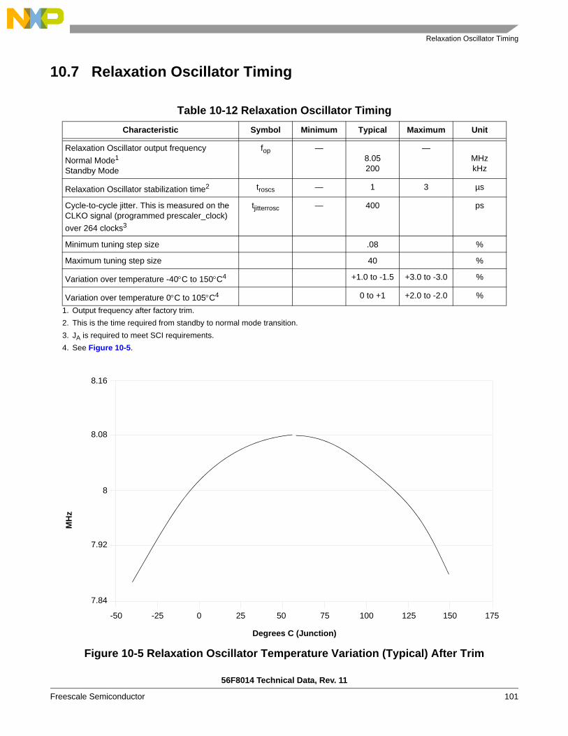
Relaxation Oscillator Timing
56F8014 Technical Data, Rev. 11
Freescale Semiconductor 101
10.7 Relaxation Oscillator Timing
Figure 10-5 Relaxation Oscillator Temperature Variation (Typical) After Trim
Table 10-12 Relaxation Oscillator TimingCharacteristic Symbol Minimum Typical Maximum Unit
Relaxation Oscillator output frequencyNormal Mode1
Standby Mode
1. Output frequency after factory trim.
fop —8.05200
—MHzkHz
Relaxation Oscillator stabilization time2
2. This is the time required from standby to normal mode transition.
troscs — 1 3 µs
Cycle-to-cycle jitter. This is measured on the CLKO signal (programmed prescaler_clock) over 264 clocks3
3. JA is required to meet SCI requirements.
tjitterrosc — 400 ps
Minimum tuning step size .08 %
Maximum tuning step size 40 %
Variation over temperature -40°C to 150°C4
4. See Figure 10-5.
+1.0 to -1.5 +3.0 to -3.0 %
Variation over temperature 0°C to 105°C4 0 to +1 +2.0 to -2.0 %
8.16
8.08
8
7.92
7.84
175-25-50 0 50 75 100 125 15025
Degrees C (Junction)
MH
z
56F8014 Technical Data, Rev. 11
102 Freescale Semiconductor
10.8 Reset, Stop, Wait, Mode Select, and Interrupt TimingNote: All the address and data buses described here are internal.
Figure 10-6 GPIO Interrupt Timing (Negative Edge-Sensitive)
Table 10-13 Reset, Stop, Wait, Mode Select, and Interrupt Timing1,2
1. In the formulas, T = clock cycle and Tosc = oscillator clock cycle. For an operating frequency of 32MHz, T = 31.25ns. At 8MHz(used during Reset and Stop modes), T = 125ns.
2. Parameters listed are guaranteed by design.
Characteristic Symbol Typical Min Typical Max Unit See Figure
Minimum RESET Assertion Duration tRA 4T — ns
Minimum GPIO pin Assertion for Interrupt tIW 2T — ns 10-6
RESET deassertion to First Address Fetch3
3. During Power-On Reset, it is possible to use the 56F8014 internal reset stretching circuitry to extend this period to 2^21T.
tRDA 96TOSC + 64T 97TOSC + 65T ns
Delay from Interrupt Assertion to Fetch of first instruction (exiting Stop)
tIF — 6T ns
GPIO pin(Input)
TIW

Serial Peripheral Interface (SPI) Timing
56F8014 Technical Data, Rev. 11
Freescale Semiconductor 103
10.9 Serial Peripheral Interface (SPI) Timing
Table 10-14 SPI Timing1
Characteristic Symbol Min Max Unit See Figure
Cycle timeMasterSlave
tC12562.5
——
nsns
10-7, 10-8, 10-9, 10-10
Enable lead timeMasterSlave
tELD—31
——
nsns
10-10
Enable lag timeMasterSlave
tELG—
125——
nsns
10-10
Clock (SCK) high timeMaster Slave
tCH5031
——
nsns
10-7, 10-8, 10-9, 10-10
Clock (SCK) low timeMaster Slave
tCL5031
——
nsns
10-10
Data set-up time required for inputsMaster Slave
tDS200
——
nsns
10-7, 10-8, 10-9, 10-10
Data hold time required for inputsMaster Slave
tDH02
——
nsns
10-7, 10-8, 10-9, 10-10
Access time (time to data active from high-impedance state)Slave
tA4.8 15 ns
10-10
Disable time (hold time to high-impedance state)Slave
tD3.7 15.2 ns
10-10
Data Valid for outputsMasterSlave (after enable edge)
tDV——
4.520.4
nsns
10-7, 10-8, 10-9, 10-10
Data invalid MasterSlave
tDI00
——
nsns
10-7, 10-8, 10-9, 10-10
Rise timeMaster Slave
tR——
11.510.0
nsns
10-7, 10-8, 10-9, 10-10
Fall time Master Slave
tF——
9.79.0
nsns
10-7, 10-8, 10-9, 10-10

56F8014 Technical Data, Rev. 11
104 Freescale Semiconductor
1
Figure 10-7 SPI Master Timing (CPHA = 0)
1. Parameters listed are guaranteed by design.
SCLK (CPOL = 0)(Output)
SCLK (CPOL = 1)(Output)
MISO(Input)
MOSI(Output)
MSB in Bits 14–1 LSB in
tF
tC
tCL
tCL
tR
tRtF
tDS
tDH tCH
tDI tDV tDI(ref)
tR
Master MSB out Bits 14–1 Master LSB out
SS(Input)
tCH
SS is held High on master
tF

Serial Peripheral Interface (SPI) Timing
56F8014 Technical Data, Rev. 11
Freescale Semiconductor 105
Figure 10-8 SPI Master Timing (CPHA = 1)
Figure 10-9 SPI Slave Timing (CPHA = 0)
SCLK (CPOL = 0)(Output)
SCLK (CPOL = 1)(Output)
MISO(Input)
MOSI(Output)
MSB in Bits 14–1 LSB in
tR
tC
tCL
tCL
tF
tCH
tDV(ref) tDV tDI(ref)
tRtF
Master MSB out Bits 14– 1 Master LSB out
SS(Input)
tCH
SS is held High on master
tDStDH
tDI
tR
tF
SCLK (CPOL = 0)(Input)
SCLK (CPOL = 1)(Input)
MISO(Output)
MOSI(Input)
Slave MSB out Bits 14–1
tC
tCL
tCL
tF
tCH
tDI
MSB in Bits 14–1 LSB in
SS(Input)
tCH
tDH
tR
tELG
tELD
tF
Slave LSB out
tDtA
tDS tDV tDI
tR

56F8014 Technical Data, Rev. 11
106 Freescale Semiconductor
Figure 10-10 SPI Slave Timing (CPHA = 1)
10.10 Quad Timer Timing
Table 10-15 Timer Timing1, 2
1. In the formulas listed, T = the clock cycle. For 32MHz operation, T = 31.25ns.2. Parameters listed are guaranteed by design.
Characteristic Symbol Min Max Unit See Figure
Timer input period PIN 2T + 6 — ns 10-11
Timer input high / low period PINHL 1T + 3 — ns 10-11
Timer output period POUT 125 — ns 10-11
Timer output high / low period POUTHL 50 — ns 10-11
SCLK (CPOL = 0)(Input)
SCLK (CPOL = 1)(Input)
MISO(Output)
MOSI(Input)
Slave MSB out Bits 14–1
tC
tCL
tCL
tCH
tDI
MSB in Bits 14–1 LSB in
SS(Input)
tCH
tDH
tF
tR
Slave LSB out
tDtA
tELD
tDV
tF
tR
tELG
tDV
tDS

Quad Timer Timing
56F8014 Technical Data, Rev. 11
Freescale Semiconductor 107
Figure 10-11 Timer Timing
POUTPOUTHL POUTHL
PINPINHL PINHL
Timer Inputs
Timer Outputs

56F8014 Technical Data, Rev. 11
108 Freescale Semiconductor
10.11 Serial Communication Interface (SCI) Timing
Figure 10-12 RXD Pulse Width
Figure 10-13 TXD Pulse Width
Table 10-16 SCI Timing1
1. Parameters listed are guaranteed by design.
Characteristic Symbol Min Max Unit See Figure
Baud Rate2
2. fMAX is the frequency of operation of the system clock in MHz, which is 32MHz for the 56F8014 device.
BR — (fMAX/16) Mbps —
RXD3 Pulse Width
3. The RXD pin in SCI0 is named RXD0 and the RXD pin in SCI1 is named RXD1.
RXDPW 0.965/BR 1.04/BR ns 10-12
TXD4 Pulse Width
4. The TXD pin in SCI0 is named TXD0 and the TXD pin in SCI1 is named TXD1.
TXDPW 0.965/BR 1.04/BR ns 10-13
LIN Slave Mode
Deviation of slave node clock from nominal clock rate before synchronization
FTOL_UNSYNCH
-14 14 %
Deviation of slave node clock relative to the master node clock after synchronization
FTOL_SYNCH -2 2 %
Minimum break character length TBREAK 13 Master node bit periods
11 Slave node bit periods
RXDPW
RXD SCI receive
data pin(Input)
TXDPW
TXD SCI receive
data pin(Input)

Inter-Integrated Circuit Interface (I2C) Timing
56F8014 Technical Data, Rev. 11
Freescale Semiconductor 109
10.12 Inter-Integrated Circuit Interface (I2C) Timing
Table 10-17 I2C Timing
Characteristic SymbolStandard Mode Fast Mode
UnitMinimum Maximum Minimum Maximum
SCL Clock Frequency fSCL 0 100 0 400 kHz
Hold time (repeated ) START condition. After this period, the first clock pulse is generated.
tHD; STA 4.0 0.6 μs
LOW period of the SCL clock tLOW 4.7 1.25 μs
HIGH period of the SCL clock tHIGH 4.0 0.6 μs
Set-up time for a repeated START condition
tSU; STA 4.7 0.6 μs
Data hold time for I2C bus devices tHD; DAT 01
1. A device must internally provide a hold time of at least 300ns for the SDA signal (referred to the VIH min of the SCL signal) tobridge the undefined region of the falling edge of SCL.
3.452
2. The maximum tHD; DAT has only to be met if the device does not stretch the LOW period (tLOW) of the SCL signal.
01 0.92 μs
Data set-up time tSU; DAT 250 1003
3. A Fast mode I2C bus device can be used in a Standard mode I2C bus system, but the requirement tSU; DAT > = 250ns must thenbe met. This will automatically be the case if the device does not stretch the LOW period of the SCL signal. If such a device doesstretch the LOW period of the SCL signal, it must output the next data bit to the SDA line trmax + tSU; DAT = 1000 + 250 = 1250ns (according to the Standard mode I2C bus specification) before the SCL line is released.
ns
Rise time of both SDA and SCL signals
tr 1000 2 +0.1Cb4
4. Cb = total capacitance of the one bus line in pF.
300 ns
Fall time of both SDA and SCL signals
tf 300 2 +0.1Cb4 300 ns
Set-up time for STOP condition tSU; STO 4.0 0.6 μs
Bus free time between STOP and START condition
tBUF 4.7 1.3 μs
Pulse width of spikes that must be suppressed by the input filter
tSP N/A N/A 0.0 50 ns

56F8014 Technical Data, Rev. 11
110 Freescale Semiconductor
Figure 10-14 Timing Definition for Fast and Standard Mode Devices on the I2C Bus
10.13 JTAG Timing
Figure 10-15 Test Clock Input Timing Diagram
Table 10-18 JTAG Timing
Characteristic Symbol Min Max Unit See Figure
TCK frequency of operation1
1. TCK frequency of operation must be less than 1/8 the processor rate.
fOP DC SYS_CLK/8 MHz 10-15
TCK clock pulse width tPW 50 — ns 10-15
TMS, TDI data set-up time tDS 5 — ns 10-16
TMS, TDI data hold time tDH 5 — ns 10-16
TCK low to TDO data valid tDV — 30 ns 10-16
TCK low to TDO tri-state tTS — 30 ns 10-16
SDA
SCL
tHD; STAtHD; DAT
tLOWtSU; DAT
tHIGH
tSU; STABR P SS
tHD; STA tSP
tSU; STO
tBUF
TCK(Input)
VM
VILVM = VIL + (VIH – VIL)/2
tPW
1/fOP
tPW
VM
VIH

JTAG Timing
56F8014 Technical Data, Rev. 11
Freescale Semiconductor 111
Figure 10-16 Test Access Port Timing Diagram
Input Data Valid
Output Data Valid
tDS tDH
tDV
tTS
TCK(Input)
TDI
(Input)
TDO(Output)
TDO(Output)
TMS

56F8014 Technical Data, Rev. 11
112 Freescale Semiconductor
10.14 Analog-to-Digital Converter (ADC) Parameters
Table 10-19 ADC Parameters1
1. All measurements were made at VDD = 3.3V, VREFH = 3.3V, and VREFL = ground
Parameter Symbol Min Typ Max Unit
DC SpecificationsResolution RES 12 — 12 Bits
ADC internal clock fADIC 0.1 — 5.33 MHz
Conversion range RAD VREFL — VREFH V
ADC power-up time2
2. Includes power-up of ADC and VREF
tADPU — 6 13 tAIC cycles3
3. ADC clock cycles
Recovery from auto standby tREC — 0 1 tAIC cycles3
Conversion time tADC — 6 — tAIC cycles3
Sample time tADS — 1 — tAIC cycles3
Accuracy
Integral non-linearity4
(Full input signal range)
4. INL measured from VIN = VREFL to VIN = VREFH
INL — +/- 3 +/- 5 LSB5
Differential non-linearity DNL — +/- .6 +/- 1 LSB5
Monotonicity GUARANTEEDOffset Voltage Internal Ref VOFFSET — +/- 4 +/- 9 mV
Offset Voltage External Ref VOFFSET — +/- 6 +/- 12 mV
Gain Error (transfer gain) EGAIN — .998 to 1.002 1.01 to .99 —
ADC Inputs6 (Pin Group 3)Input voltage (external reference) VADIN VREFL — VREFH V
Input voltage (internal reference) VADIN VSSA — VDDA V
Input leakage IIA — 0 +/- 2 μA
VREFH current IVREFH — 0 — μA
Input injection current7, per pin IADI — — 3 mA
Input capacitance CADI — See Figure 10-17 — pF
Input impedance XIN — See Figure 10-17 — Ohms
AC SpecificationsSignal-to-noise ratio SNR 60 65 dBTotal Harmonic Distortion THD 60 64 dBSpurious Free Dynamic Range SFDR 61 66 dBSignal-to-noise plus distortion SINAD 58 62 dBEffective Number Of Bits ENOB — 10.0 Bits

Equivalent Circuit for ADC Inputs
56F8014 Technical Data, Rev. 11
Freescale Semiconductor 113
10.15 Equivalent Circuit for ADC InputsFigure 10-17 illustrates the ADC input circuit during sample and hold. S1 and S2 are always open/closedat the same time that S3 is closed/open. When S1/S2 are closed & S3 is open, one input of the sample andhold circuit moves to (VREFH-VREFL)/2, while the other charges to the analog input voltage. When theswitches are flipped, the charge on C1 and C2 are averaged via S3, with the result that a single-endedanalog input is switched to a differential voltage centered about (VREFH-VREFL)/2. The switches switchon every cycle of the ADC clock (open one-half ADC clock, closed one-half ADC clock). Note that thereare additional capacitances associated with the analog input pad, routing, etc., but these do not filter intothe S/H output voltage, as S1 provides isolation during the charge-sharing phase.
One aspect of this circuit is that there is an on-going input current, which is a function of the analog inputvoltage, VREF and the ADC clock frequency.
5. LSB = Least Significant Bit = 0.806mV6. Pin groups are detailed following Table 10-1.7. The current that can be injected or sourced from an unselected ADC signal input without impacting the performance of the
ADC.

56F8014 Technical Data, Rev. 11
114 Freescale Semiconductor
1. Parasitic capacitance due to package, pin-to-pin and pin-to-package base coupling; 1.8pF2. Parasitic capacitance due to the chip bond pad, ESD protection devices and signal routing; 2.04pF3. Equivalent resistance for the channel select mux; 100 ohms 4. Sampling capacitor at the sample and hold circuit. Capacitor C1 is normally disconnected from the input and is only
connected to it at sampling time; 1.4pf5. Equivalent input impedance, when the the input is selected =
Figure 10-17 Equivalent Circuit for A/D Loading
10.16 Power ConsumptionSee Section 10.1 for a list of IDD requirements for the 56F8014. This section provides additional detailwhich can be used to optimize power consumption for a given application.
Power consumption is given by the following equation:
Total power = A: internal [static component]+B: internal [state-dependent component]
125 OhmESD Resistor
Equivalent Circuit for A/D Loading
channel muxequiv resistance100 Ohms
(VREFHx - VREFLx) / 2
C1
S/H
S1
1 2 3
ADC Input
1. Parasitic capacitance due to package, pin-to-pin and pin-to-package base coupling; 1.8 pF
2. Parasitic capacitance due to the chip bond pad, ESD protection devices and signal routing; 2.04pF
3. 8 pF noise damping capacitor4. C1 = 1.4 pF5. S1 and S2 switch phases are non-overlapping and operate at the ADC
clock frequency
S1
S2 S2
C1 : Singled Ended Mode 2 X C1 : Differential Mode
S1
S1
C1
C1 : Singled Ended Mode 2 X C1 : Differential Mode
S1
S2
6. Equivalent input impedance, when the input is selected = ohmohmRateClockADC
12510012104.1)(1 ++−××
1
(ADC Clock Rate) x 1.4 x 10⁻¹²
Please see http://www.freescale.com for the most current mechanical drawing.

Power Consumption
56F8014 Technical Data, Rev. 11
Freescale Semiconductor 115
A, the internal [static component], is comprised of the DC bias currents for the oscillator, leakage currents,PLL, and voltage references. These sources operate independently of processor state or operatingfrequency.
B, the internal [state-dependent component], reflects the supply current required by certain on-chipresources only when those resources are in use. These include RAM, Flash memory and the ADCs.
C, the internal [dynamic component], is classic C*V2*F CMOS power dissipation corresponding to the56800E core and standard cell logic.
D, the external [dynamic component], reflects power dissipated on-chip as a result of capacitive loadingon the external pins of the chip. This is also commonly described as C*V2*F, although simulations on twoof the I/O cell types used on the 56800E reveal that the power-versus-load curve does have a non-zeroY-intercept.
Power due to capacitive loading on output pins is (first order) a function of the capacitive load andfrequency at which the outputs change. Table 10-20 provides coefficients for calculating power dissipatedin the I/O cells as a function of capacitive load. In these cases:
TotalPower = Σ((Intercept + Slope*Cload)*frequency/10MHz)
where:
• Summation is performed over all output pins with capacitive loads• TotalPower is expressed in mW• Cload is expressed in pF
Because of the low duty cycle on most device pins, power dissipation due to capacitive loads was foundto be fairly low when averaged over a period of time.
E, the external [static component], reflects the effects of placing resistive loads on the outputs of thedevice. Sum the total of all V2/R or IV to arrive at the resistive load contribution to power. Assume V = 0.5for the purposes of these rough calculations. For instance, if there is a total of eight PWM outputs driving10mA into LEDs, then P = 8*.5*.01 = 40mW.
+C: internal [dynamic component]+D: external [dynamic component]+E: external [static]
Table 10-20 I/O Loading Coefficients at 10MHz
Intercept Slope
8mA drive 1.3 0.11mW / pF
4mA drive 1.15mW 0.11mW / pF

56F8014 Technical Data, Rev. 11
116 Freescale Semiconductor
In previous discussions, power consumption due to parasitics associated with pure input pins is ignored,as it is assumed to be negligible.

56F8014 Package and Pin-Out Information
56F8014 Technical Data, Rev. 11
Freescale Semiconductor 117
Part 11 Packaging
11.1 56F8014 Package and Pin-Out Information This section contains package and pin-out information for the 56F8014. This device comes in a 32-pinLow-profile Quad Flat Pack (LQFP). Figure 11-1 shows the package outline for the 32-pin LQFP,Figure 11-2 shows the mechanical parameters for this package, and Table 11-1 lists the pin-out for the32-pin LQFP.
Figure 11-1 Top View, 56F8014 32-Pin LQFP Package
PIN 1
ORIENTATIONMARK
PIN 25
PIN 17PIN 9
GPIOB1/SS/SDA
GPIOB7/TXD/SCL
GPIOB5/T1/FAULT3
ANB0/GPIOC4
ANB1/GPIOC5
ANB2/VREFL/GPIOC6
ANB3/GPIOC7
VDDA GPIOB3/MOSI/T3
GPIOB2/MISO/T2
GPIOB4/T0/CLKO
GPIOA5/PWM5/FAULT2/T3
GPIOB0/SCLK/SCL
GPIOA4/PWM4/FAULT1/T2
GPIOA2/PWM2
VCAP
GPI
OA
0/P
WM
0
V DD
_IO
GPI
OA
1/P
WM
1
V SS_
IO
TDI/G
PIO
D0
TMS/
GP
IOD
3
TDO
/GP
IOD
1
GPI
OB
6/R
XD
/SD
A/C
LKIN
V SSA
AN
A3/
GPI
OC
3
AN
A2/
VR
EFH
/GPI
OC
2
AN
A1/
GPI
OC
1
AN
A0/
GPI
OC
0
V SS_
IO
TCK
/GPI
OD
2
RES
ET/G
PIO
A7
Note: Alternate signals are in italic
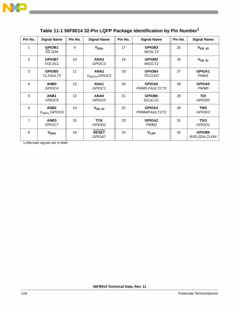
56F8014 Technical Data, Rev. 11
118 Freescale Semiconductor
Table 11-1 56F8014 32-Pin LQFP Package Identification by Pin Number1
1.Alternate signals are in iltalic
Pin No. Signal Name Pin No. Signal Name Pin No. Signal Name Pin No. Signal Name
1 GPIOB1SS,SDA
9 VSSA 17 GPIOB3MOSI,T3
25 VDD_IO
2 GPIOB7TXD,SCL
10 ANA3GPIOC3
18 GPIOB2MISO,T2
26 VSS_IO
3 GPIOB5T1,FAULT3
11 ANA2VREFH,GPIOC2
19 GPIOB4T0,CLKO
27 GPIOA1PWM1
4 ANB0GPIOC4
12 ANA1GPIOC1
20 GPIOA5PWM5,FAULT2,T3
28 GPIOA0PWM0
5 ANB1GPIOC5
13 ANA0GPIOC0
21 GPIOB0SCLK/,CL
29 TDIGPIOD0
6 ANB2VREFL,GPIOC6
14 VSS_IO 22 GPIOA4PWM4/FAULT1/T2
30 TMSGPIOD3
7 ANB3GPIOC7
15 TCKGPIOD2
23 GPIOA2PWM2
31 TDOGPIOD1
8 VDDA 16 RESETGPIOA7
24 VCAP 32 GPIOB6RXD,SDA,CLKIN
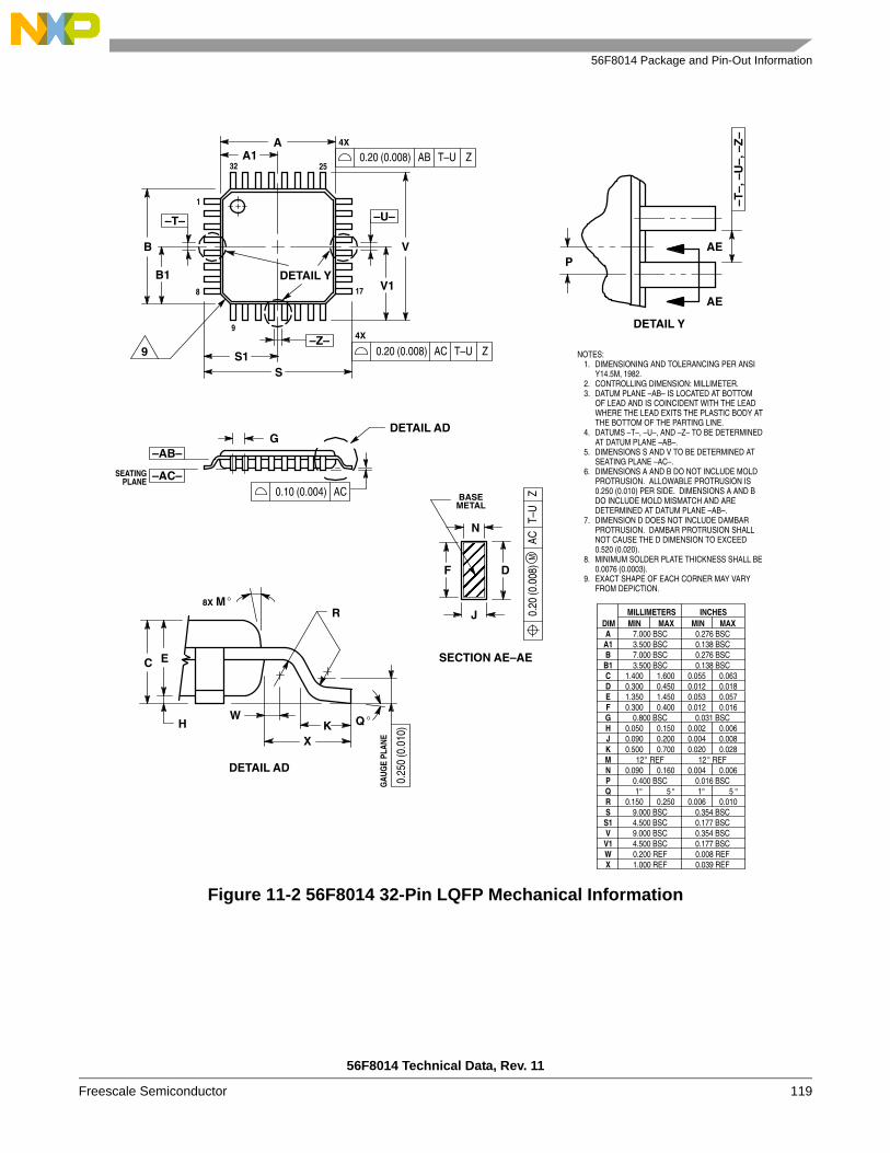
56F8014 Package and Pin-Out Information
56F8014 Technical Data, Rev. 11
Freescale Semiconductor 119
Figure 11-2 56F8014 32-Pin LQFP Mechanical Information
ÉÉÉÉÉÉÉÉ
DETAIL Y
A
S1
VB
1
8
9
17
2532
AE
AE
P
DETAIL Y
BASE
N
J
DF
METAL
SECTION AE–AE
G
SEATINGPLANE
R
QWK
X
0.25
0 (0
.010
)
GAU
GE
PLAN
E
EC
H
DETAIL AD
NOTES:1. DIMENSIONING AND TOLERANCING PER ANSI
Y14.5M, 1982.2. CONTROLLING DIMENSION: MILLIMETER.3. DATUM PLANE –AB– IS LOCATED AT BOTTOM
OF LEAD AND IS COINCIDENT WITH THE LEADWHERE THE LEAD EXITS THE PLASTIC BODY ATTHE BOTTOM OF THE PARTING LINE.
4. DATUMS –T–, –U–, AND –Z– TO BE DETERMINEDAT DATUM PLANE –AB–.
5. DIMENSIONS S AND V TO BE DETERMINED ATSEATING PLANE –AC–.
6. DIMENSIONS A AND B DO NOT INCLUDE MOLDPROTRUSION. ALLOWABLE PROTRUSION IS0.250 (0.010) PER SIDE. DIMENSIONS A AND BDO INCLUDE MOLD MISMATCH AND AREDETERMINED AT DATUM PLANE –AB–.
7. DIMENSION D DOES NOT INCLUDE DAMBARPROTRUSION. DAMBAR PROTRUSION SHALLNOT CAUSE THE D DIMENSION TO EXCEED0.520 (0.020).
8. MINIMUM SOLDER PLATE THICKNESS SHALL BE0.0076 (0.0003).
9. EXACT SHAPE OF EACH CORNER MAY VARYFROM DEPICTION.
DIMA
MIN MAX MIN MAXINCHES
7.000 BSC 0.276 BSC
MILLIMETERS
B 7.000 BSC 0.276 BSC
C 1.400 1.600 0.055 0.063D 0.300 0.450 0.012 0.018E 1.350 1.450 0.053 0.057F 0.300 0.400 0.012 0.016G 0.800 BSC 0.031 BSCH 0.050 0.150 0.002 0.006J 0.090 0.200 0.004 0.008K 0.500 0.700 0.020 0.028M 12 REF 12 REFN 0.090 0.160 0.004 0.006P 0.400 BSC 0.016 BSCQ 1 5 1 5 R 0.150 0.250 0.006 0.010
V 9.000 BSC 0.354 BSCV1 4.500 BSC 0.177 BSC
DETAIL AD
A1
B1V1
4X
S
4X
B1 3.500 BSC 0.138 BSC
A1 3.500 BSC 0.138 BSC
S 9.000 BSC 0.354 BSCS1 4.500 BSC 0.177 BSC
W 0.200 REF 0.008 REFX 1.000 REF 0.039 REF
9
–T–
–Z–
–U–
T–U0.20 (0.008) ZAC
T–U0.20 (0.008) ZAB
0.10 (0.004) AC–AC–
–AB–
M8X
–T–,
–U
–, –
Z–
T–U
M0.
20 (0
.008
)Z
AC

56F8014 Technical Data, Rev. 11
120 Freescale Semiconductor
Part 12 Design Considerations
12.1 Thermal Design ConsiderationsAn estimation of the chip junction temperature, TJ, can be obtained from the equation:
TJ = TA + (RθJΑ x PD)where:
The junction-to-ambient thermal resistance is an industry-standard value that provides a quick and easyestimation of thermal performance. Unfortunately, there are two values in common usage: the valuedetermined on a single-layer board and the value obtained on a board with two planes. For packages suchas the PBGA, these values can be different by a factor of two. Which value is closer to the applicationdepends on the power dissipated by other components on the board. The value obtained on a single layerboard is appropriate for the tightly packed printed circuit board. The value obtained on the board with theinternal planes is usually appropriate if the board has low-power dissipation and the components are wellseparated.
When a heat sink is used, the thermal resistance is expressed as the sum of a junction-to-case thermalresistance and a case-to-ambient thermal resistance:
RθJA = RθJC + RθCAwhere:
RθJC is device related and cannot be influenced by the user. The user controls the thermal environment tochange the case to ambient thermal resistance, RθCA. For instance, the user can change the size of the heatsink, the air flow around the device, the interface material, the mounting arrangement on printed circuitboard, or change the thermal dissipation on the printed circuit board surrounding the device.
To determine the junction temperature of the device in the application when heat sinks are not used, theThermal Characterization Parameter (ΨJT) can be used to determine the junction temperature with ameasurement of the temperature at the top center of the package case using the following equation:
TJ = TT + (ΨJT x PD)where:
TA = Ambient temperature for the package (oC)RθJΑ = Junction-to-ambient thermal resistance (oC/W)PD = Power dissipation in the package (W)
RθJA = Package junction-to-ambient thermal resistance (°C/W)RθJC = Package junction-to-case thermal resistance (°C/W)RθCA = Package case-to-ambient thermal resistance (°C/W)
TT = Thermocouple temperature on top of package (oC)

Electrical Design Considerations
56F8014 Technical Data, Rev. 11
Freescale Semiconductor 121
The thermal characterization parameter is measured per JESD51-2 specification using a 40-gauge type Tthermocouple epoxied to the top center of the package case. The thermocouple should be positioned sothat the thermocouple junction rests on the package. A small amount of epoxy is placed over thethermocouple junction and over about 1mm of wire extending from the junction. The thermocouple wireis placed flat against the package case to avoid measurement errors caused by cooling effects of thethermocouple wire.
When heat sink is used, the junction temperature is determined from a thermocouple inserted at theinterface between the case of the package and the interface material. A clearance slot or hole is normallyrequired in the heat sink. Minimizing the size of the clearance is important to minimize the change inthermal performance caused by removing part of the thermal interface to the heat sink. Because of theexperimental difficulties with this technique, many engineers measure the heat sink temperature and thenback-calculate the case temperature using a separate measurement of the thermal resistance of theinterface. From this case temperature, the junction temperature is determined from the junction-to-casethermal resistance.
12.2 Electrical Design Considerations
Use the following list of considerations to assure correct operation of the 56F8014:
• Provide a low-impedance path from the board power supply to each VDD pin on the 56F8014 and from the board ground to each VSS (GND) pin
• The minimum bypass requirement is to place 0.01–0.1μF capacitors positioned as close as possible to the package supply pins. The recommended bypass configuration is to place one bypass capacitor on each of the VDD/VSS pairs, including VDDA/VSSA. Ceramic and tantalum capacitors tend to provide better tolerances.
• Ensure that capacitor leads and associated printed circuit traces that connect to the chip VDD and VSS (GND) pins are as short as possible
• Bypass the VDD and VSS with approximately 100μF, plus the number of 0.1μF ceramic capacitors
ΨJT = Thermal characterization parameter (oC/W)PD = Power dissipation in package (W)
CAUTION
This device contains protective circuitry to guardagainst damage due to high static voltage or electricalfields. However, normal precautions are advised toavoid application of any voltages higher thanmaximum-rated voltages to this high-impedance circuit.Reliability of operation is enhanced if unused inputs aretied to an appropriate voltage level.

56F8014 Technical Data, Rev. 11
122 Freescale Semiconductor
• PCB trace lengths should be minimal for high-frequency signals• Consider all device loads as well as parasitic capacitance due to PCB traces when calculating capacitance.
This is especially critical in systems with higher capacitive loads that could create higher transient currents in the VDD and VSS circuits.
• Take special care to minimize noise levels on the VREF, VDDA and VSSA pins
• Using separate power planes for VDD and VDDA and separate ground planes for VSS and VSSA is recommended. Connect the separate analog and digital power and ground planes as close as possible to power supply outputs. If both analog circuit and digital circuit are powered by the same power supply, it is advisable to connect a small inductor or ferrite bead in serial with both VDDA and VSSA traces.
• It is highly desirable to physically separate analog components from noisy digital components by ground planes. Do not place an analog trace in parallel with digital traces. It is also desirable to place an analog ground trace around an analog signal trace to isolate it from digital traces.
• Because the Flash memory is programmed through the JTAG/EOnCE port, SPI, SCI or I2C, the designer should provide an interface to this port if in-circuit Flash programming is desired.

Electrical Design Considerations
56F8014 Technical Data, Rev. 11
Freescale Semiconductor 123
Part 13 Ordering InformationTable 13-1 lists the pertinent information needed to place an order. Consult a Freescale Semiconductorsales office or authorized distributor to determine availability and to order parts.
*This package is RoHS compliant.
Part 14 Appendix Register acronyms are revised from previous device data sheets to provide a cleaner register description.A cross reference to legacy and revised acronyms are provided in the following table.
Table 13-1 56F8014 Ordering Information
Part SupplyVoltage Package Type Pin
CountFrequency
(MHz)
AbientTemperature
RangeOrder Number
MC56F8014 3.0–3.6 V Low-Profile Quad Flat Pack (LQFP) 32 32 -40° to + 105° C MC56F8014VFAE*
MC56F8014 3.0–3.6 V Low-Profile Quad Flat Pack (LQFP) 32 32 –40° to +125 °C MC56F8014MFAE*
Module Register Name
Peripheral Reference Manual Data Sheet Processor Expert
Acronym
Memory Address
New Acronym Legacy Acronym New Acronym Legacy Acronym Start End
ADC Control Register 1 CTRL1 ADCR1 ADC_CTRL1 ADC_ADCR1 ADC_ADCR1 0xF080Control Register 2 CTRL2 ADCR2 ADC_CTRL2 ADC_ADCR2 ADC_ADCR2 0xF081Zero Crossing Control Register ZXCTRL ADZCC ADC_ZXCTRL ADC_ADZCC ADC_ADZCC 0xF082Channel List Register 1 CLIST1 ADLST1 ADC_CLIST1 ADC_ADLST1 ADC_ADLST1 0xF083Channel List Register 2 CLIST2 ADLST2 ADC_CLIST2 ADC_ADLST2 ADC_ADLST2 0xF084Sample Disable Register SDIS ADSDIS ADC_SDIS ADC_ADSDIS ADC_ADSDIS 0xF085Status Register STAT ADSTAT ADC_STAT ADC_ADSTAT ADC_ADSTAT 0xF086Limit Status Register LIMSTAT ADLSTAT ADC_LIMSTAT ADC_ADLSTAT ADC_ADLSTAT 0xF087Zero Crossing Status Register ZXSTAT ADZCSTAT ADC_ZXSTAT ADC_ADZCSTAT ADC_ADZCSTAT 0xF088Result Registers 0-7 RSLT0-7 ADRSLT0-7 ADC_RSLT0-7 ADC_ADRSLT0-7 ADC_ADRSLT0-7 0xF089 0XF090Low Limit Registers 0-7 LOLIM0-7 ADLLMT0-7 ADC_LOLIM0-7 ADC_ADLLMT0-7 ADC_ADLLMT0-7 0XF091 0XF098High Limit Registers 0-7 HILIM0-7 ADHLMT0-7 ADC_HILIM0-7 ADC_ADHLMT0-7 ADC_ADHLMT0-7 0XF099 0XF0A0Offset Registers 0-7 OFFST0-7 ADOFS0-7 ADC_OFFST0-7 ADC_ADOFS0-7 ADC_ADOFS0-7 0XF0A1 0XF0A8Power Control Register PWR ADPOWER ADC_PWR ADC_ADPOWER ADC_ADPOWER 0XF0A9Voltage Reference Register CAL ADCAL ADC_VREF ADC_ADCAL ADC_CAL 0XF0AA
COP Control Register CTRL COPCTL COP_CTRL COPCTL COPCTL 0XF0E0Time-Out Register TOUT COPTO COP_TOUT COPTO COPTO 0XF0E1Counter Register CNTR COPCTR COP_CNTR COPCTR COPCTR 0XF0E2

How to Reach Us:
Home Page:www.freescale.com
E-mail:[email protected]
USA/Europe or Locations Not Listed:Freescale SemiconductorTechnical Information Center, CH3701300 N. Alma School RoadChandler, Arizona 85224+1-800-521-6274 or [email protected]
Europe, Middle East, and Africa:Freescale Halbleiter Deutschland GmbHTechnical Information CenterSchatzbogen 781829 Muenchen, Germany+44 1296 380 456 (English)+46 8 52200080 (English)+49 89 92103 559 (German)+33 1 69 35 48 48 (French)[email protected]
Japan:Freescale Semiconductor Japan Ltd.HeadquartersARCO Tower 15F1-8-1, Shimo-Meguro, Meguro-ku,Tokyo 153-0064, Japan0120 191014 or +81 3 5437 [email protected]
Asia/Pacific:Freescale Semiconductor Hong Kong Ltd.Technical Information Center2 Dai King StreetTai Po Industrial EstateTai Po, N.T., Hong Kong+800 2666 [email protected]
For Literature Requests Only:Freescale Semiconductor Literature Distribution CenterP.O. Box 5405Denver, Colorado 802171-800-441-2447 or 303-675-2140Fax: [email protected]
Freescale™ and the Freescale logo are trademarks of Freescale Semiconductor, Inc. All other product or service names are the property of their respective owners.This product incorporates SuperFlash® technology licensed from SST.© Freescale Semiconductor, Inc. 2005. All rights reserved.
MC56F8014Rev. 1105/2008
Information in this document is provided solely to enable system and software implementers to use Freescale Semiconductor products. There are no express or implied copyright licenses granted hereunder to design or fabricate any integrated circuits or integrated circuits based on the information in this document.
Freescale Semiconductor reserves the right to make changes without further notice to any products herein. Freescale Semiconductor makes no warranty, representation or guarantee regarding the suitability of its products for any particular purpose, nor does Freescale Semiconductor assume any liability arising out of the application or use of any product or circuit, and specifically disclaims any and all liability, including without limitation consequential or incidental damages. “Typical” parameters that may be provided in Freescale Semiconductor data sheets and/or specifications can and do vary in different applications and actual performance may vary over time. All operating parameters, including “Typicals”, must be validated for each customer application by customer’s technical experts. Freescale Semiconductor does not convey any license under its patent rights nor the rights of others. Freescale Semiconductor products are not designed, intended, or authorized for use as components in systems intended for surgical implant into the body, or other applications intended to support or sustain life, or for any other application in which the failure of the Freescale Semiconductor product could create a situation where personal injury or death may occur. Should Buyer purchase or use Freescale Semiconductor products for any such unintended or unauthorized application, Buyer shall indemnify and hold Freescale Semiconductor and its officers, employees, subsidiaries, affiliates, and distributors harmless against all claims, costs, damages, and expenses, and reasonable attorney fees arising out of, directly or indirectly, any claim of personal injury or death associated with such unintended or unauthorized use, even if such claim alleges that Freescale Semiconductor was negligent regarding the design or manufacture of the part.
RoHS-compliant and/or Pb-free versions of Freescale products have the functionality and electrical characteristics of their non-RoHS-compliant and/or non-Pb-free counterparts. For further information, see http://www.freescale.com or contact your Freescale sales representative.
For information on Freescale’s Environmental Products program, go to http://www.freescale.com/epp.

Mouser Electronics
Authorized Distributor
Click to View Pricing, Inventory, Delivery & Lifecycle Information: NXP:
DEMO56F8014-EE MC56F8014MFAE MC56F8014VFAE