5052H data sheet(English) - NPC · 5052H series Crystal Oscillator Module ICs SEIKO NPC CORPORATION...
14
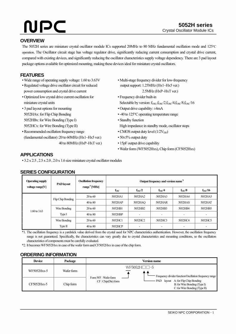
5052H series Crystal Oscillator Module ICs SEIKO NPC CORPORATION - 1 OVERVIEW The 5052H series are miniature crystal oscillator module ICs supported 20MHz to 80 MHz fundamental oscillation mode and 125 °C operation . The Oscillator circuit stage has voltage regulator drive, significantly reducing current consumption and crystal drive current, compared with existing devices, and significantly reducing the oscillator characteristics supply voltage dependency. There are 3 pad layout package options available for optimized mounting, making these devices ideal for miniature crystal oscillators. FEATURES ▪ Wide range of operating supply voltage: 1.60 to 3.63V ▪ Multi-stage frequency divider for low-frequency ▪ Regulated voltage drive oscillator circuit for reduced output support: 1.25MHz (Hx1~Hx5 ver.) power consumption and crystal drive current 2.5MHz (HxP~HxT ver.) ▪ Optimized low crystal drive current oscillation for ▪ Frequency divider built-in miniature crystal units Selectable by version: f OSC ,f OSC /2,f OSC /4,f OSC /8,f OSC /16 ▪ 3 pad layout options for mounting ▪ Output drive capability: ±4mA 5052HAx: for Flip Chip Bonding ▪ -40 to 125°C operating temperature range 5052HBx: for Wire Bonding (Type I) ▪ Standby function 5052HCx: for Wire Bonding (Type II) High impedance in standby mode, oscillator stops ▪ Recommended oscillation frequency range ▪ CMOS output duty level (1/2V DD ) (fundamental oscillator) :20 to 60MHz (Hx1~Hx5 ver.) ▪ 50±5% output duty 40 to 80MHz (HxP~HxT ver.) ▪ 15pF output drive capability ▪ Wafer form (WF5052Hxx), Chip form (CF5052Hxx) APPLICATIONS ▪ 3.2 x 2.5 , 2.5 x 2.0 , 2.0 x 1.6 size miniature crystal oscillator modules SERIES CONFIGURATION Output frequency and version name *2 Operating supply voltage range[V] PAD layout Oscillation frequency range *1 [MHz] f OSC f OSC /2 f OSC /4 f OSC /8 f OSC /16 20 to 60 5052HA1 5052HA2 5052HA3 5052HA4 5052HA5 Flip Chip Bonding 40 to 80 5052HAP 5052HAQ 5052HAR 5052HAS 5052HAT 20 to 60 5052HB1 5052HB2 5052HB3 5052HB4 5052HB5 Wire Bonding Type I 40 to 80 5052HBP - - - - 20 to 60 5052HC1 5052HC2 5052HC3 5052HC4 5052HC5 1.60 to 3.63 Wire Bonding Type II 40 to 80 5052HCP - - - - *1. The oscillation frequency is a yardstick value derived from the crystal used for NPC characteristics authentication. However, the oscillation frequency range is not guaranteed. Specifically, the characteristics can vary greatly due to crystal characteristics and mounting conditions, so the oscillation characteristics of components must be carefully evaluated. *2. It becomes WF5052Hxx in case of the wafer form and CF5052Hxx in case of the chip form. ORDERING INFORMATION Device Package Version name WF5052Hxx-5 Wafer form CF5052Hxx-5 Chip form WF5052H□□-5 PAD layout A: for Flip Chip Bonding B: for Wire Bonding (Type I) C: for Wire Bonding (Type II) Frequency divider function/Oscillation frequency range Form WF : Wafer form CF : Chip(Die) form
Transcript of 5052H data sheet(English) - NPC · 5052H series Crystal Oscillator Module ICs SEIKO NPC CORPORATION...
5052H series Crystal Oscillator Module ICs
SEIKO NPC CORPORATION - 1
OVERVIEW The 5052H series are miniature crystal oscillator module ICs supported 20MHz to 80 MHz fundamental oscillation mode and 125°C
operation. The Oscillator circuit stage has voltage regulator drive, significantly reducing current consumption and crystal drive current,
compared with existing devices, and significantly reducing the oscillator characteristics supply voltage dependency. There are 3 pad layout
package options available for optimized mounting, making these devices ideal for miniature crystal oscillators.
FEATURES Wide range of operating supply voltage: 1.60 to 3.63V Multi-stage frequency divider for low-frequency Regulated voltage drive oscillator circuit for reduced output support: 1.25MHz (Hx1~Hx5 ver.)
power consumption and crystal drive current 2.5MHz (HxP~HxT ver.) Optimized low crystal drive current oscillation for Frequency divider built-in
miniature crystal units Selectable by version: fOSC,fOSC/2,fOSC/4,fOSC/8,fOSC/16
3 pad layout options for mounting Output drive capability: ±4mA
5052HAx: for Flip Chip Bonding -40 to 125°C operating temperature range
5052HBx: for Wire Bonding (Type I) Standby function
5052HCx: for Wire Bonding (Type II) High impedance in standby mode, oscillator stops
Recommended oscillation frequency range CMOS output duty level (1/2VDD)
(fundamental oscillator) :20 to 60MHz (Hx1~Hx5 ver.) 50±5% output duty
40 to 80MHz (HxP~HxT ver.) 15pF output drive capability
Wafer form (WF5052Hxx), Chip form (CF5052Hxx)
APPLICATIONS 3.2 x 2.5 , 2.5 x 2.0 , 2.0 x 1.6 size miniature crystal oscillator modules
SERIES CONFIGURATION
Output frequency and version name*2 Operating supply
voltage range[V] PAD layout
Oscillation frequency
range*1 [MHz] fOSC fOSC/2 fOSC/4 fOSC/8 fOSC/16
20 to 60 5052HA1 5052HA2 5052HA3 5052HA4 5052HA5 Flip Chip Bonding
40 to 80 5052HAP 5052HAQ 5052HAR 5052HAS 5052HAT
20 to 60 5052HB1 5052HB2 5052HB3 5052HB4 5052HB5 Wire Bonding
Type I 40 to 80 5052HBP - - - -
20 to 60 5052HC1 5052HC2 5052HC3 5052HC4 5052HC5
1.60 to 3.63
Wire Bonding
Type II 40 to 80 5052HCP - - - -
*1. The oscillation frequency is a yardstick value derived from the crystal used for NPC characteristics authentication. However, the oscillation frequency range is not guaranteed. Specifically, the characteristics can vary greatly due to crystal characteristics and mounting conditions, so the oscillation characteristics of components must be carefully evaluated.
*2. It becomes WF5052Hxx in case of the wafer form and CF5052Hxx in case of the chip form.
ORDERING INFORMATION
Device Package Version name
WF5052Hxx-5 Wafer form
CF5052Hxx-5 Chip form
WF5052H-5
PAD layout A: for Flip Chip Bonding B: for Wire Bonding (Type I) C: for Wire Bonding (Type II)
Frequency divider function/Oscillation frequency range Form WF : Wafer form CF : Chip(Die) form

5052H series
SEIKO NPC CORPORATION - 2
PAD LAYOUT WF5052HAx CF5052HBx CF5052HCx
(for Flip Chip Bonding) (for Wire Bonding (Type I)) (for Wire Bonding (Type II))
1 2
3
45
6
(-300,-285)
(300,285)
XT XTN
VDD
Q VSS
INHN
X
Y (0,0)
Chip size : 0.60x0.57mm
Chip thickness : 100μm
PAD size : 80μm
Chip base : VSS level
1 2
3
45
6
(-300,-285)
(300,285)
XTN XT
INHN
VSS Q
VDD
X
Y (0,0)
Chip size : 0.60x0.57mm
Chip thickness : 100μm
PAD size : 80μm
Chip base : VSS level
1 2
3
45
6
(-300,-285)
(300,285)
XT XTN
VSS
Q VDD
INHN
X
Y (0,0)
Chip size : 0.60x0.57mm
Chip thickness : 100μm
PAD size : 80μm
Chip base : VSS level
· Coordinates at the chip center are (0,0).
PAD COORDINATES PIN DESCRIPTION
PAD coordinate[μm] PAD No. PAD
No. X Y 5052HAx 5052HBx 5052HCx
Pin Function
1 -145.2 -193.5 1 2 1 XT
2 145.2 -193.5 2 1 2 XTN
Crystal connection pins.
Crystal is connected between XT and XTN.
3 208.5 -1.1 3 6 5 VDD (+)supply voltage
4 208.5 193.5 4 5 4 Q Output one of fOSC,fOSC/2,fOSC/4,fOSC/8,fOSC/16
5 -208.5 193.5 5 4 3 VSS (-)ground
6 -208.5 -1.1
6 3 6 INHNInput pin controlled output state(oscillator stops when
LOW), Power-saving pull-up resistor built-in
BLOCK DIAGRAM
INHN
XT
XTN
VDD
Q
CG CD
RF
RD
VRG
1N
N=1,2,4,8,16
VSS
CMOS
5052H series
SEIKO NPC CORPORATION - 3
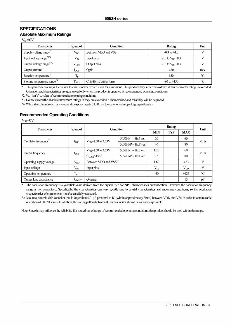
SPECIFICATIONS Absolute Maximum Ratings VSS=0V
Parameter Symbol Condition Rating Unit
Supply voltage range*1 VDD Between VDD and VSS -0.3 to +4.0 V
Input voltage range*1*2 VIN Input pins -0.3 to VDD+0.3 V
Output voltage range*1*2 VOUT Output pins -0.3 to VDD+0.3 V
Output current*3 IOUT Q pin ±20 mA
Junction temperature*3 Tj 150 °C
Storage temperature range*4 TSTG Chip form, Wafer form -65 to +150 °C
*1. This parameter rating is the values that must never exceed even for a moment. This product may suffer breakdown if this parameter rating is exceeded. Operation and characteristics are guaranteed only when the product is operated at recommended operating conditions.
*2. VDD is a VDD value of recommended operating conditions. *3. Do not exceed the absolute maximum ratings. If they are exceeded, a characteristic and reliability will be degraded. *4. When stored in nitrogen or vacuum atmosphere applied to IC itself only (excluding packaging materials).
Recommended Operating Conditions VSS=0V
Rating Parameter Symbol Condition
MIN TYP MAX Unit
5052Hx1 ~ Hx5 ver. 20 60 Oscillator frequency*1 fOSC VDD=1.60 to 3.63V
5052HxP ~ HxT ver. 40 80 MHz
5052Hx1 ~ Hx5 ver. 1.25 60 Output frequency fOUT
VDD=1.60 to 3.63V
CLOUT≤15pF 5052HxP ~ HxTver. 2.5 80 MHz
Operating supply voltage VDD Between VDD and VSS*2 1.60 3.63 V
Input voltage VIN Input pins VSS VDD V
Operating temperature Ta -40 +125 °C
Output load capacitance CLOUT Q output 15 pF
*1. The oscillation frequency is a yardstick value derived from the crystal used for NPC characteristics authentication. However, the oscillation frequency range is not guaranteed. Specifically, the characteristics can vary greatly due to crystal characteristics and mounting conditions, so the oscillation characteristics of components must be carefully evaluated.
*2. Mount a ceramic chip capacitor that is larger than 0.01μF proximal to IC (within approximately 3mm) between VDD and VSS in order to obtain stable operation of 5052H series. In addition, the wiring pattern between IC and capacitor should be as wide as possible.
Note. Since it may influence the reliability if it is used out of range of recommended operating conditions, this product should be used within this range.
5052H series
SEIKO NPC CORPORATION - 4
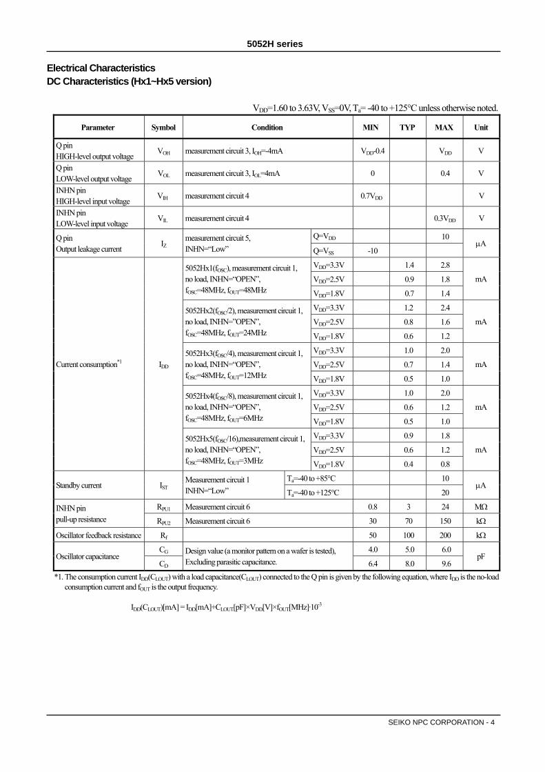
Electrical Characteristics DC Characteristics (Hx1~Hx5 version) VDD=1.60 to 3.63V, VSS=0V, Ta= -40 to +125°C unless otherwise noted.
Parameter Symbol Condition MIN TYP MAX Unit
Q pin HIGH-level output voltage
VOH measurement circuit 3, IOH=-4mA VDD-0.4 VDD V
Q pin LOW-level output voltage
VOL measurement circuit 3, IOL=4mA 0 0.4 V
INHN pin HIGH-level input voltage
VIH measurement circuit 4 0.7VDD V
INHN pin LOW-level input voltage
VIL measurement circuit 4 0.3VDD V
Q=VDD 10 Q pin Output leakage current
IZ measurement circuit 5, INHN=“Low” Q=VSS -10
A
VDD=3.3V 1.4 2.8
VDD=2.5V 0.9 1.8 5052Hx1(fOSC), measurement circuit 1, no load, INHN=“OPEN”, fOSC=48MHz, fOUT=48MHz VDD=1.8V 0.7 1.4
mA
VDD=3.3V 1.2 2.4
VDD=2.5V 0.8 1.6 5052Hx2(fOSC/2), measurement circuit 1, no load, INHN=”OPEN”, fOSC=48MHz, fOUT=24MHz VDD=1.8V 0.6 1.2
mA
VDD=3.3V 1.0 2.0
VDD=2.5V 0.7 1.4 5052Hx3(fOSC/4), measurement circuit 1, no load, INHN=“OPEN”, fOSC=48MHz, fOUT=12MHz VDD=1.8V 0.5 1.0
mA
VDD=3.3V 1.0 2.0
VDD=2.5V 0.6 1.2 5052Hx4(fOSC/8), measurement circuit 1, no load, INHN=“OPEN”, fOSC=48MHz, fOUT=6MHz VDD=1.8V 0.5 1.0
mA
VDD=3.3V 0.9 1.8
VDD=2.5V 0.6 1.2
Current consumption*1 IDD
5052Hx5(fOSC/16),measurement circuit 1,no load, INHN=“OPEN”, fOSC=48MHz, fOUT=3MHz VDD=1.8V 0.4 0.8
mA
Ta=-40 to +85°C 10 Standby current IST
Measurement circuit 1 INHN=“Low” Ta=-40 to +125°C 20
A
RPU1 Measurement circuit 6 0.8 3 24 M INHN pin pull-up resistance RPU2 Measurement circuit 6 30 70 150 k
Oscillator feedback resistance Rf 50 100 200 k
CG 4.0 5.0 6.0 Oscillator capacitance
CD
Design value (a monitor pattern on a wafer is tested), Excluding parasitic capacitance. 6.4 8.0 9.6
pF
*1. The consumption current IDD(CLOUT) with a load capacitance(CLOUT) connected to the Q pin is given by the following equation, where IDD is the no-load consumption current and fOUT is the output frequency.
IDD(CLOUT)[mA] = IDD[mA]+CLOUT[pF]×VDD[V]×fOUT[MHz]·10-3

5052H series
SEIKO NPC CORPORATION - 5
DC Characteristics (HxP~HxT version)
VDD=1.60 to 3.63V, VSS=0V, Ta= -40 to +125°C unless otherwise noted.
Parameter Symbol Condition MIN TYP MAX Unit
Q pin HIGH-level output voltage
VOH measurement circuit 3, IOH=-4mA VDD-0.4 VDD V
Q pin LOW-level output voltage
VOL measurement circuit 3, IOL=4mA 0 0.4 V
INHN pin HIGH-level input voltage
VIH measurement circuit 4 0.7VDD V
INHN pin LOW-level input voltage
VIL measurement circuit 4 0.3VDD V
Q=VDD 10 Q pin Output leakage current
IZ measurement circuit 5, INHN=“Low” Q=VSS -10
A
VDD=3.3V 2.4 4.8
VDD=2.5V 1.7 3.4 5052HxP(fOSC), measurement circuit 1, no load, INHN=“OPEN”, fOSC=80MHz, fOUT=80MHz VDD=1.8V 1.3 2.6
mA
VDD=3.3V 2.0 4.0
VDD=2.5V 1.3 2.6 5052HxQ(fOSC/2), measurement circuit 1,no load, INHN=”OPEN”, fOSC=80MHz, fOUT=40MHz VDD=1.8V 0.9 1.8
mA
VDD=3.3V 1.7 3.4
VDD=2.5V 1.1 2.2 5052HxR(fOSC/4), measurement circuit 1,no load, INHN=“OPEN”, fOSC=80MHz, fOUT=20MHz VDD=1.8V 0.8 1.6
mA
VDD=3.3V 1.5 3.0
VDD=2.5V 0.9 1.8 5052HxS(fOSC/8), measurement circuit 1, no load, INHN=“OPEN”, fOSC=80MHz, fOUT=10MHz VDD=1.8V 0.7 1.4
mA
VDD=3.3V 1.4 2.8
VDD=2.5V 0.9 1.8
Current consumption*1 IDD
5052HxT(fOSC/16),measurement circuit 1,no load, INHN=“OPEN”, fOSC=80MHz, fOUT=5MHz VDD=1.8V 0.7 1.4
mA
Ta=-40 to +85°C 10 Standby current IST
Measurement circuit 1 INHN=“Low” Ta=-40 to +125°C 20
A
RPU1 Measurement circuit 6 0.8 3 24 M INHN pin pull-up resistance RPU2 Measurement circuit 6 30 70 150 k
Oscillator feedback resistance Rf 50 100 200 k
CG 1.6 2.0 2.4 Oscillator capacitance
CD
Design value (a monitor pattern on a wafer is tested), Excluding parasitic capacitance. 2.4 3.0 3.6
pF
*1. The consumption current IDD(CLOUT) with a load capacitance(CLOUT) connected to the Q pin is given by the following equation, where IDD is the no-load consumption current and fOUT is the output frequency.
IDD(CLOUT)[mA] = IDD[mA]+CLOUT[pF]×VDD[V]×fOUT[MHz]·10-3
5052H series
SEIKO NPC CORPORATION - 6
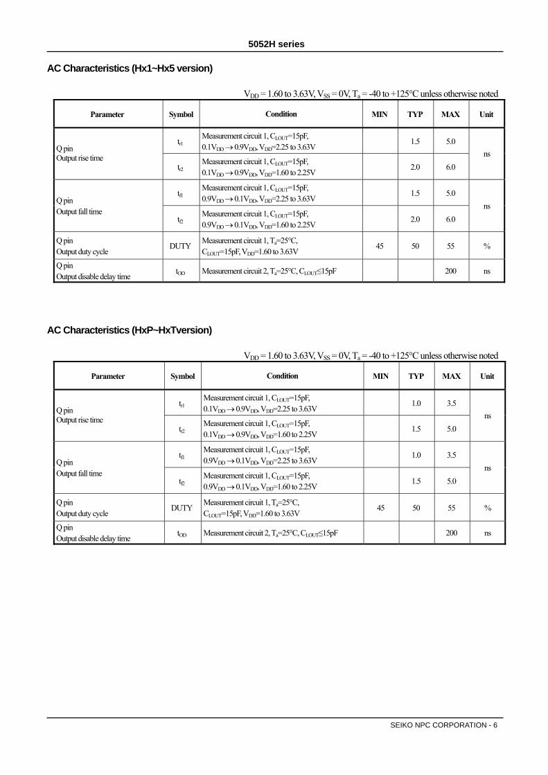
AC Characteristics (Hx1~Hx5 version) VDD = 1.60 to 3.63V, VSS = 0V, Ta = -40 to +125°C unless otherwise noted
Parameter Symbol Condition MIN TYP MAX Unit
tr1 Measurement circuit 1, CLOUT=15pF, 0.1VDD 0.9VDD, VDD=2.25 to 3.63V
1.5 5.0 Q pin Output rise time
tr2 Measurement circuit 1, CLOUT=15pF, 0.1VDD 0.9VDD, VDD=1.60 to 2.25V
2.0 6.0
ns
tf1 Measurement circuit 1, CLOUT=15pF, 0.9VDD 0.1VDD, VDD=2.25 to 3.63V
1.5 5.0 Q pin Output fall time
tf2 Measurement circuit 1, CLOUT=15pF, 0.9VDD 0.1VDD, VDD=1.60 to 2.25V
2.0 6.0
ns
Q pin Output duty cycle
DUTY Measurement circuit 1, Ta=25°C, CLOUT=15pF, VDD=1.60 to 3.63V
45 50 55 %
Q pin Output disable delay time
tOD Measurement circuit 2, Ta=25°C, CLOUT≤15pF 200 ns
AC Characteristics (HxP~HxTversion) VDD = 1.60 to 3.63V, VSS = 0V, Ta = -40 to +125°C unless otherwise noted
Parameter Symbol Condition MIN TYP MAX Unit
tr1 Measurement circuit 1, CLOUT=15pF, 0.1VDD 0.9VDD, VDD=2.25 to 3.63V
1.0 3.5 Q pin Output rise time
tr2 Measurement circuit 1, CLOUT=15pF, 0.1VDD 0.9VDD, VDD=1.60 to 2.25V
1.5 5.0
ns
tf1 Measurement circuit 1, CLOUT=15pF, 0.9VDD 0.1VDD, VDD=2.25 to 3.63V
1.0 3.5 Q pin Output fall time
tf2 Measurement circuit 1, CLOUT=15pF, 0.9VDD 0.1VDD, VDD=1.60 to 2.25V
1.5 5.0
ns
Q pin Output duty cycle
DUTY Measurement circuit 1, Ta=25°C, CLOUT=15pF, VDD=1.60 to 3.63V
45 50 55 %
Q pin Output disable delay time
tOD Measurement circuit 2, Ta=25°C, CLOUT≤15pF 200 ns

5052H series
SEIKO NPC CORPORATION - 7
Timing chart
0.1VDD 0.1VDD
0.9VDD 0.9VDD
Tw
T
tftr
Q DUTY measurement voltage 0.5VDD DUTY = Tw/T×100 (%)
Figure 1. Output switching waveform
0.5VDD
Low fOUTfOUT
VIH
VIL
VDD
VSS
Hi-Z
Q
tOD 0.1V
0.1V
VDD
VSS
INHN
When INHN goes HIGH to LOW, the Q output becomes high impedance. When INHN goes LOW to HIGH, the Q output goes LOW once and then becomes normal output operation after having detected oscillation signals.
Figure 2. Output disable and oscillation start timing chart
5052H series
SEIKO NPC CORPORATION - 8
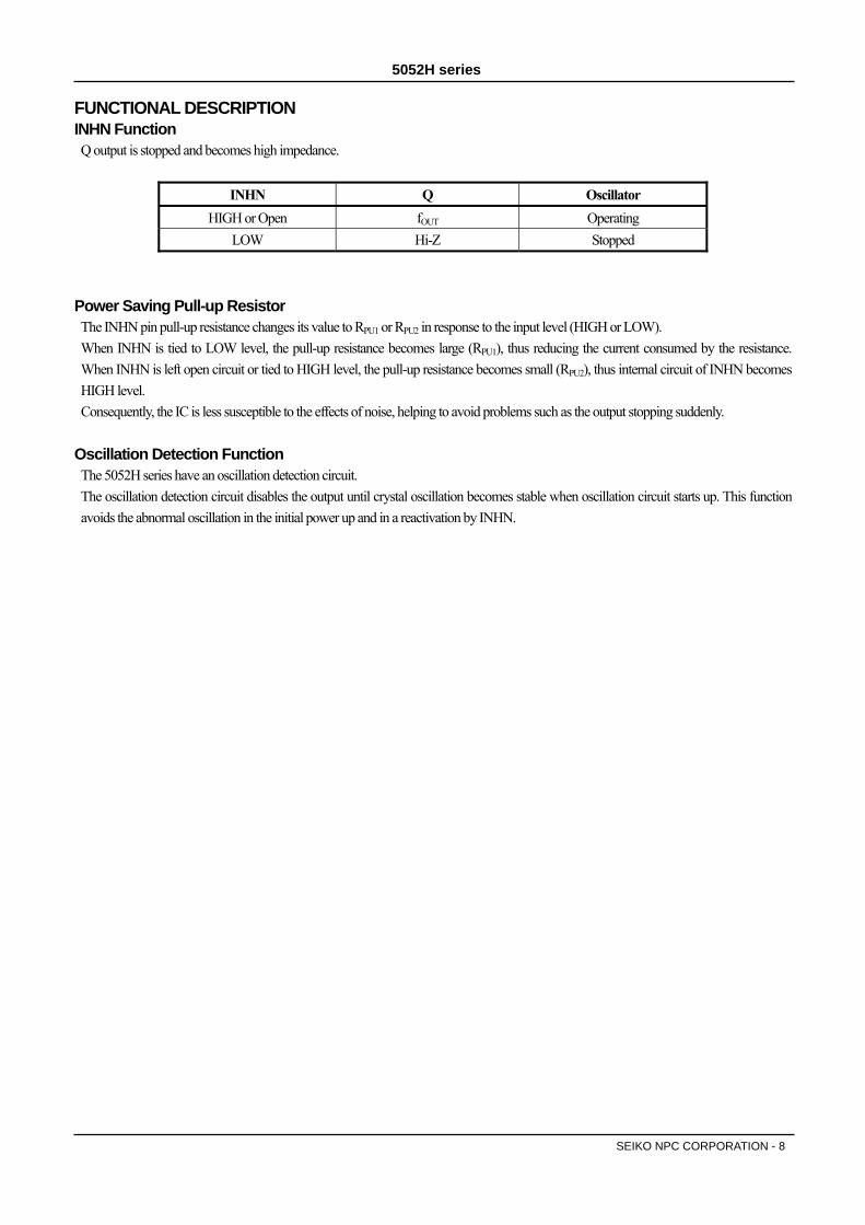
FUNCTIONAL DESCRIPTION INHN Function Q output is stopped and becomes high impedance.
INHN Q Oscillator
HIGH or Open fOUT Operating
LOW Hi-Z Stopped
Power Saving Pull-up Resistor The INHN pin pull-up resistance changes its value to RPU1 or RPU2 in response to the input level (HIGH or LOW).
When INHN is tied to LOW level, the pull-up resistance becomes large (RPU1), thus reducing the current consumed by the resistance.
When INHN is left open circuit or tied to HIGH level, the pull-up resistance becomes small (RPU2), thus internal circuit of INHN becomes
HIGH level.
Consequently, the IC is less susceptible to the effects of noise, helping to avoid problems such as the output stopping suddenly.
Oscillation Detection Function The 5052H series have an oscillation detection circuit.
The oscillation detection circuit disables the output until crystal oscillation becomes stable when oscillation circuit starts up. This function
avoids the abnormal oscillation in the initial power up and in a reactivation by INHN.
5052H series
SEIKO NPC CORPORATION - 9
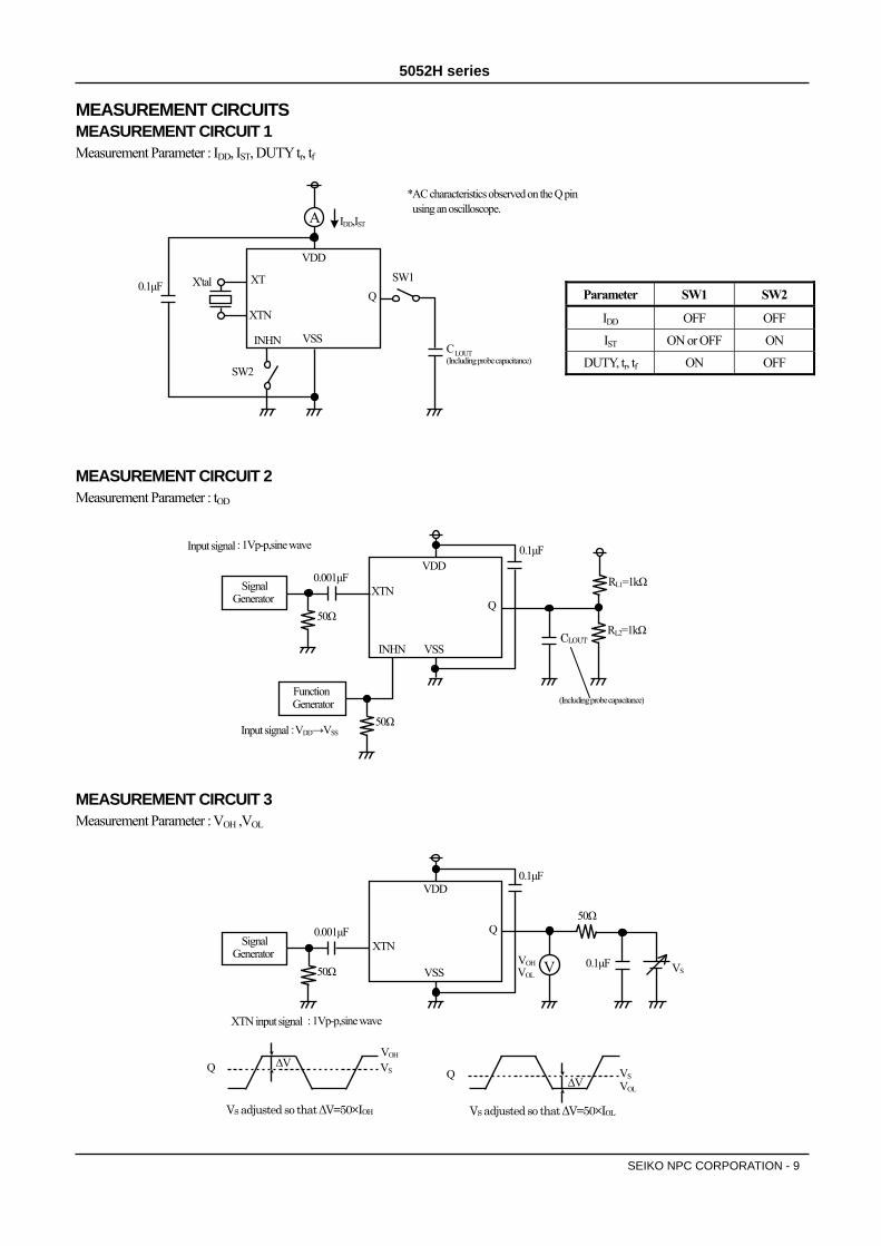
MEASUREMENT CIRCUITS MEASUREMENT CIRCUIT 1 Measurement Parameter : IDD, IST, DUTY tr, tf
Parameter SW1 SW2
IDD OFF OFF
IST ON or OFF ON
DUTY, tr, tf ON OFF
MEASUREMENT CIRCUIT 2 Measurement Parameter : tOD
MEASUREMENT CIRCUIT 3 Measurement Parameter : VOH ,VOL
(Including probe capacitance)
X'tal XT
INHN
XTN Q
VDD
VSS
A
SW2
IDD,IST
CLOUT
SW1 0.1μF
*AC characteristics observed on the Q pin using an oscilloscope.
RL1=1kΩ
RL2=1kΩ
Q
VDD
VSS
Signal Generator XTN
50Ω
0.001μF
0.1μF
Function Generator
50Ω
INHNCLOUT
(Including probe capacitance)
Input signal : 1Vp-p,sine wave
:Input signal VDD→VSS
Q
VDD
VSS
Signal Generator
VVOH VOL
XTN
VS
VS VOH
ΔV VS VOL ΔV
50Ω
50Ω
0.001μF
0.1μF
0.1μF
Q Q
XTN input signal : 1Vp-p,sine wave
VS adjusted so that ΔV=50×IOH VS adjusted so that ΔV=50×IOL

5052H series
SEIKO NPC CORPORATION - 10
MEASUREMENT CIRCUIT 4 Measurement Parameter : VIH, VIL
MEASUREMENT CIRCUIT 5 Measurement Parameter : IZ
XT
INHN
XTN Q
VDD
VSS
VIH, VIL
X'tal
V
0.1μF
VIH: VSS→VDD voltage that changes output state VIL: VDD→VSS voltage that changes output state
INHN
Q
VDD
VSS
A
IZ
VDD or
VSS
0.1μF
MEASUREMENT CIRCUIT 6 Measurement Parameter : RPU1, RPU2
INHN
VDD
VSS
AV VIN IPU
RPU1 =
RPU2 =
VDD
IPU
VDD 0.7VDD IPU
(VIN = 0V)
(VIN = 0.7VDD )
0.1μF

5052H series
SEIKO NPC CORPORATION - 11
REFERENCE DATA The following characteristics are measured using the crystal below. Note that the characteristics will vary with the crystal used.
Crystal used for measurement Crystal parameters
Parameter 40MHz 48MHz 80MHz
C0(pF) 1.4 1.8 3.2
R1(Ω) 8 7 13 C0
L1 C1 R1
Current Consumption
0.0
0.5
1.0
1.5
2.0
2.5
3.0
3.5
4.0
1.5 2.0 2.5 3.0 3.5 4VDD [V]
IDD [
mA
]
0.0
0.5
1.0
1.5
2.0
2.5
3.0
3.5
4.0
1.5 2.0 2.5 3.0 3.5 4VDD [V]
IDD [
mA
]
.0 .0
5052Hx1, fOSC=48MHz, Ta=25C, no load 5052HxP, fOSC=80MHz, Ta=25C, no load
Negative Resistance
-2000
-1500
-1000
-500
0
10 20 30 40 50 60Frequency [MHz]
Neg
ativ
e R
esis
tanc
e [Ω
]
C0: none
C0: 1pF
C0: 2pF
-2000
-1500
-1000
-500
0
20 30 40 50 60 70 80Frequency [MHz]
Neg
ativ
e R
esis
tanc
e [Ω
]
C0: 2pF
C0: none
C0: 1pF
5052Hx1, VDD=3.3V, Ta=25C 5052HxP, VDD=3.3V, Ta=25C
Measurement equipment: Agilent Impedance analyzer 4396B
They may vary in a measurement jig, and measurement environment.
The figures show the measurement result of the crystal equivalent circuit C0 capacitance, connected between the XT and XTN pins.
They were performed with Agilent 4396B using the NPC test jig.
5052H series
SEIKO NPC CORPORATION - 12
Frequency Deviation by Voltage
-1.0
-0.5
0.0
0.5
1.0
1.5 2.0 2.5 3.0 3.5 4.0VDD[V]
Fre
quen
cy d
evia
tion
[pp
m]]
-1.0
-0.5
0.0
0.5
1.0
1.5 2.0 2.5 3.0 3.5 4.0VDD[V]
Fre
quen
cy d
evia
tion
[pp
m]]
5052Hx1, fOSC=40MHz, Ta=25C, 2.5V std. 5052HxP, fOSC=80MHz, Ta=25C, 2.5V std.
Drive Level
0
20
40
60
80
100
1.5 2.0 2.5 3.0 3.5 4.0VDD [V]
Dri
ve L
evel
[μ
W]]
0
20
40
60
80
100
1.5 2.0 2.5 3.0 3.5 4.0VDD [V]
Dri
ve L
evel
[μ
W]]
5052Hx1, fOSC=40MHz, Ta=25C 5052HxP, fOSC=80MHz, Ta=25C
Phase Noise
-180
-160
-140
-120
-100
-80
-60
1.0E+01 1.0E+02 1.0E+03 1.0E+04 1.0E+05 1.0E+06 1.0E+07 1.0E+08Offset Frequency [Hz]
Pha
se N
oise
[dB
c/H
z]]
-180
-160
-140
-120
-100
-80
-60
1.0E+01 1.0E+02 1.0E+03 1.0E+04 1.0E+05 1.0E+06 1.0E+07 1.0E+08Offset Frequency [Hz]
Pha
se N
oise
[dB
c/H
z]]
5052Hx1, fOSC=40MHz, VDD=3.3V, Ta=25C 5052HxP, fOSC=80MHz, VDD=3.3V, Ta=25C
Measurement equipment: Signal Source Analyzer Agilent E5052B
5052H series
SEIKO NPC CORPORATION - 13
Output Waveform
5.00ns
550mV
5052Hx1 version, VDD=3.3V, fOUT=40MHz, CLOUT=15pF, Ta: Room temperature
550mV
2.50ns
5052HxP version, VDD=3.3V, fOUT=80MHz, CLOUT=15pF, Ta: Room temperature Measurement equipment: Oscilloscope Agilent DSO80604B

5052H series
SEIKO NPC CORPORATION - 14
Please pay your attention to the following points at time of using the products shown in this document. 1. The products shown in this document (hereinafter ”Products”) are designed and manufactured to the generally accepted standards of
reliability as expected for use in general electronic and electrical equipment, such as personal equipment, machine tools and measurement equipment. The Products are not designed and manufactured to be used in any other special equipment requiring extremely high level of reliability and safety, such as aerospace equipment, nuclear power control equipment, medical equipment, transportation equipment, disaster prevention equipment, security equipment. The Products are not designed and manufactured to be used for the apparatus that exerts harmful influence on the human lives due to the defects, failure or malfunction of the Products.
If you wish to use the Products in that apparatus, please contact our sales section in advance. In the event that the Products are used in such apparatus without our prior approval, we assume no responsibility whatsoever for any
damages resulting from the use of that apparatus. 2. NPC reserves the right to change the specifications of the Products in order to improve the characteristics or reliability thereof. 3. The information described in this document is presented only as a guide for using the Products. No responsibility is assumed by us for any
infringements of patents or other rights of the third parties which may result from its use. No license is granted by implication or otherwise under any patents or other rights of the third parties. Then, we assume no responsibility whatsoever for any damages resulting from that infringements.
4. The constant of each circuit shown in this document is described as an example, and it is not guaranteed about its value of the mass production products.
5. In the case of that the Products in this document falls under the foreign exchange and foreign trade control law or other applicable laws and regulations, approval of the export to be based on those laws and regulations are necessary. Customers are requested appropriately take steps to obtain required permissions or approvals from appropriate government agencies.
SEIKO NPC CORPORATION 1-9-9, Hatchobori, Chuo-ku, Tokyo 104-0032, Japan Telephone: +81-3-5541-6501 Facsimile: +81-3-5541-6510 http://www.npc.co.jp/ Email:[email protected] ND12015-E-00 2012.07