5-V PECL-to-TTL Translator datasheet - TI.com · pecl dc characteristics ttl dc characteristics ac...
13
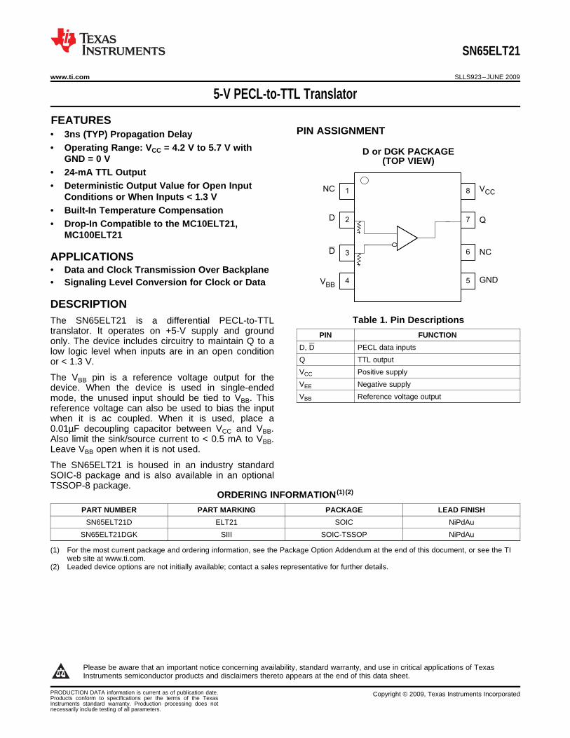
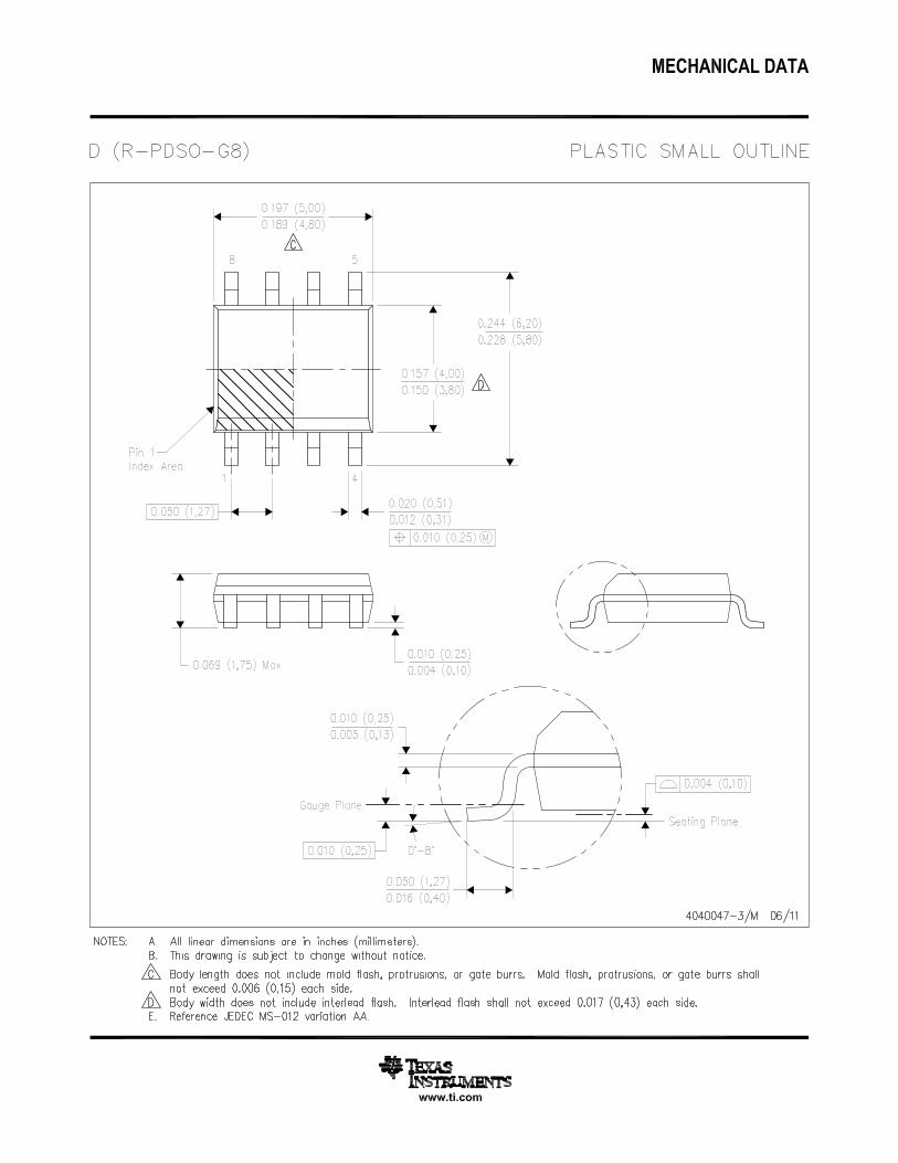
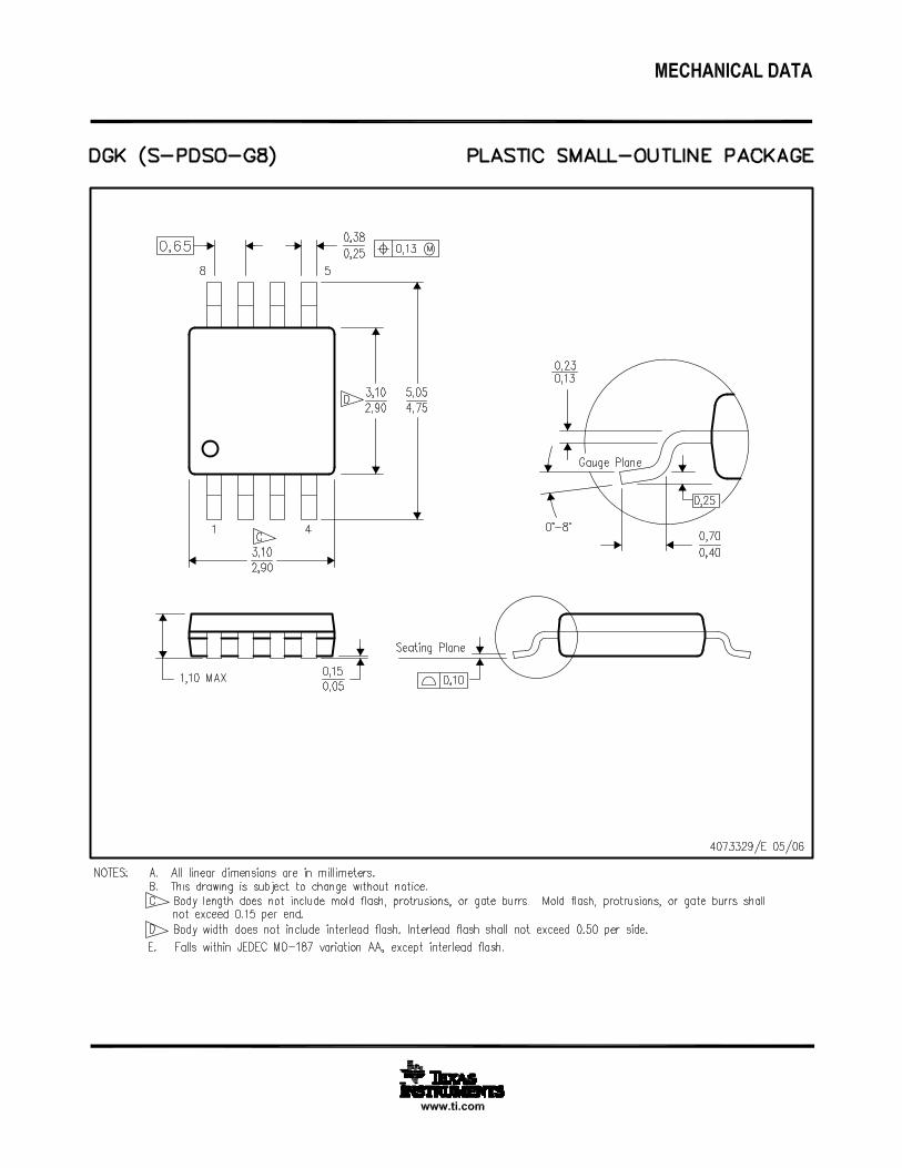
1FEATURES PIN ASSIGNMENT APPLICATIONS 1 8 2 7 3 6 4 5 NC Q NC V CC D D GND V BB DESCRIPTION SN65ELT21 www.ti.com....................................................................................................................................................................................................... SLLS923–JUNE 2009 5-V PECL-to-TTL Translator • 3ns (TYP) Propagation Delay • Operating Range: V CC = 4.2 V to 5.7 V with D or DGK PACKAGE GND = 0 V (TOP VIEW) • 24-mA TTL Output • Deterministic Output Value for Open Input Conditions or When Inputs < 1.3 V • Built-In Temperature Compensation • Drop-In Compatible to the MC10ELT21, MC100ELT21 • Data and Clock Transmission Over Backplane • Signaling Level Conversion for Clock or Data Table 1. Pin Descriptions The SN65ELT21 is a differential PECL-to-TTL translator. It operates on +5-V supply and ground PIN FUNCTION only. The device includes circuitry to maintain Q to a D, D PECL data inputs low logic level when inputs are in an open condition Q TTL output or < 1.3 V. V CC Positive supply The V BB pin is a reference voltage output for the V EE Negative supply device. When the device is used in single-ended V BB Reference voltage output mode, the unused input should be tied to V BB . This reference voltage can also be used to bias the input when it is ac coupled. When it is used, place a 0.01μF decoupling capacitor between V CC and V BB . Also limit the sink/source current to < 0.5 mA to V BB . Leave V BB open when it is not used. The SN65ELT21 is housed in an industry standard SOIC-8 package and is also available in an optional TSSOP-8 package. ORDERING INFORMATION (1) (2) PART NUMBER PART MARKING PACKAGE LEAD FINISH SN65ELT21D ELT21 SOIC NiPdAu SN65ELT21DGK SIII SOIC-TSSOP NiPdAu (1) For the most current package and ordering information, see the Package Option Addendum at the end of this document, or see the TI web site at www.ti.com. (2) Leaded device options are not initially available; contact a sales representative for further details. 1 Please be aware that an important notice concerning availability, standard warranty, and use in critical applications of Texas Instruments semiconductor products and disclaimers thereto appears at the end of this data sheet. PRODUCTION DATA information is current as of publication date. Copyright © 2009, Texas Instruments Incorporated Products conform to specifications per the terms of the Texas Instruments standard warranty. Production processing does not necessarily include testing of all parameters.
Transcript of 5-V PECL-to-TTL Translator datasheet - TI.com · pecl dc characteristics ttl dc characteristics ac...
1FEATURESPIN ASSIGNMENT
APPLICATIONS
1 8
2 7
3 6
4 5
NC
Q
NC
VCC
D
D
GNDVBB
DESCRIPTION
SN65ELT21
www.ti.com ....................................................................................................................................................................................................... SLLS923–JUNE 2009
5-V PECL-to-TTL Translator
• 3ns (TYP) Propagation Delay• Operating Range: VCC = 4.2 V to 5.7 V with D or DGK PACKAGE
GND = 0 V (TOP VIEW)• 24-mA TTL Output• Deterministic Output Value for Open Input
Conditions or When Inputs < 1.3 V• Built-In Temperature Compensation• Drop-In Compatible to the MC10ELT21,
MC100ELT21
• Data and Clock Transmission Over Backplane• Signaling Level Conversion for Clock or Data
Table 1. Pin DescriptionsThe SN65ELT21 is a differential PECL-to-TTLtranslator. It operates on +5-V supply and ground PIN FUNCTIONonly. The device includes circuitry to maintain Q to a
D, D PECL data inputslow logic level when inputs are in an open conditionQ TTL outputor < 1.3 V.VCC Positive supplyThe VBB pin is a reference voltage output for theVEE Negative supplydevice. When the device is used in single-endedVBB Reference voltage outputmode, the unused input should be tied to VBB. This
reference voltage can also be used to bias the inputwhen it is ac coupled. When it is used, place a0.01µF decoupling capacitor between VCC and VBB.Also limit the sink/source current to < 0.5 mA to VBB.Leave VBB open when it is not used.
The SN65ELT21 is housed in an industry standardSOIC-8 package and is also available in an optionalTSSOP-8 package.
ORDERING INFORMATION (1) (2)
PART NUMBER PART MARKING PACKAGE LEAD FINISHSN65ELT21D ELT21 SOIC NiPdAu
SN65ELT21DGK SIII SOIC-TSSOP NiPdAu
(1) For the most current package and ordering information, see the Package Option Addendum at the end of this document, or see the TIweb site at www.ti.com.
(2) Leaded device options are not initially available; contact a sales representative for further details.
1
Please be aware that an important notice concerning availability, standard warranty, and use in critical applications of TexasInstruments semiconductor products and disclaimers thereto appears at the end of this data sheet.
PRODUCTION DATA information is current as of publication date. Copyright © 2009, Texas Instruments IncorporatedProducts conform to specifications per the terms of the TexasInstruments standard warranty. Production processing does notnecessarily include testing of all parameters.
ABSOLUTE MAXIMUM RATINGS (1)
DISSIPATION RATINGS
THERMAL CHARACTERISTICS
KEY ATTRIBUTES
SN65ELT21
SLLS923–JUNE 2009....................................................................................................................................................................................................... www.ti.com
These devices have limited built-in ESD protection. The leads should be shorted together or the device placed in conductive foamduring storage or handling to prevent electrostatic damage to the MOS gates.
PARAMETER CONDITIONS VALUE UNITAbsolute PECL mode supply voltage VCC (GND = 0 V) 6 VSink/source current, VBB ±0.5 mAPECL input voltage GND = 0 V, VI ≤ VCC 6 VOperating temperature range –40 to 85 °CStorage temperature range –65 to 150 °C
(1) Stresses beyond those listed under absolute maximum ratings may cause permanent damage to the device. These are stress ratingsonly and functional operation of the device at these or any conditions beyond those indicated under recommended operating conditionsis not implied. Exposure to absolute-maximum-rated conditions for extended periods may affect device reliability.
POWER RATING THERMAL RESISTANCE, DERATING FACTOR POWER RATINGCIRCUIT BOARD JUNCTION-TO-AMBIENTPACKAGE TA < 25°C TA > 25°C TA = 85°CMODEL NO AIRFLOW(mW) (mW/°C) (mW)
SOIC Low-K 719 139 7 288High-K 840 119 8 336
SOIC-TSSOP Low-K 469 213 5 188High-K 527 189 5 211
over operating free-air temperature range (unless otherwise noted)
PARAMETER MIN TYP MAX UNITθJB Junction-to-board thermal resistance SOIC 79 °C/W
SOIC-TSSOP 120θJC Junction-to-case thermal resistance SOIC 98 °C/W
SOIC-TSSOP 74
CHARACTERISTICS VALUEInternal input pull-down resistor 50 kΩMoisture sensitivity level Level 1Flame ability rating (oxygen index: 28 to 34) UL 94 V-0 at 0.125 inElectrostatic discharge Human body model 2 kV
Charged-device model 1.5 kVMeets or exceeds JEDEC Spec EIA/JESD78 latchup test
2 Submit Documentation Feedback Copyright © 2009, Texas Instruments Incorporated
Product Folder Link(s): SN65ELT21
PECL DC CHARACTERISTICS
TTL DC CHARACTERISTICS
AC CHARACTERISTICS
SN65ELT21
www.ti.com ....................................................................................................................................................................................................... SLLS923–JUNE 2009
At VCC = 5.0 V, GND = 0.0 V (unless otherwise noted) (1) (2)
TA = –40°C TA = 25°C TA = 85°CPARAMETER TEST CONDITIONS UNIT
MIN TYP MAX MIN TYP MAX MIN TYP MAXVIH High-level input voltage, 3835 4120 3835 4120 3835 4120 mV
single-endedVIL Low-leveI input voltage, 3190 3525 3190 3525 3190 3525 mV
single-endedVBB Output reference voltage 3.62 3.69 3.74 3.62 3.69 3.74 3.62 3.69 3.74 VVIHCMR High-level input voltage, See (3) 2.2 5.0 2.2 5.0 2.2 5.0 V
common-mode range,differential
IIH High-level input current 150 150 150 µAIIL Low-level input current 0.5 0.5 0.5 µA
(1) The device will meet the specifications after thermal balance has been established when mounted in a socket or printed circuit boardwith maintained transverse airflow greater than 500 lfpm. Electrical parameters are assured only over the declared operatingtemperature range. Functional operation of the device exceeding these conditions is not implied. Device specification limit values areapplied individually under normal operating conditions and not valid simultaneously.
(2) Input parameters vary 1:1 with VCC. VCC can vary +0.7 V / –0.8 V.(3) VIHCMR(min) varies 1:1 with GND, VIHCMR(max) varies 1:1 with VCC.
At VCC = 4.2 V to 5.7 V, TA = –40°C to 85°C (unless otherwise noted) (1)
PARAMETER TEST CONDITIONS MIN TYP MAX UNITICCH Power supply current 20 mAICCL Power supply current 20 mAVOH High-level output voltage IOH = –3.0 mA 2.4 See (2) VVOL Low-level output voltage IOL = 24 mA 0.5 VIOS Output short circuit current –150 –60 mA
(1) The device will meet the specifications after thermal balance has been established when mounted in a socket or printed circuit boardwith maintained transverse airflow greater than 500 lfpm. Electrical parameters are assured only over the declared operatingtemperature range. Functional operation of the device exceeding these conditions is not implied. Device specification limit values areapplied individually under normal operating conditions and not valid simultaneously.
(2) VOH(max) level is VCC – 0.7.
At VCC = 4.2 V to 5.7 V, GND = 0.0 V (unless otherwise noted) (1) (2)
TA = –40°C TA = 25°C TA = 85°CTESTPARAMETER UNITCONDITIONS MIN TYP MAX MIN TYP MAX MIN TYP MAXfMAX Maximum switching At Vol < 0.5V 200 200 200 MHz
frequency (See Figure 4)tPLH/tPHL Propagation delay times At 1.5 V 2 4.5 2 4.5 2 4.5 nstJITTER Random clock jitter (RMS) 5 20 5 20 5 20 psVPP Input swing See (3) 200 1000 200 1000 200 1000 mVtr/tf Output rise/fall times Q (10%–90%) 750 780 910 ps
(1) The device will meet the specifications after thermal equilibrium has been established when mounted in a test socket or printed circuitboard with maintained transverse airflow greater than 500 lfpm. Electrical parameters are assured only over the declared operatingtemperature range. Functional operation of the device exceeding these conditions is not implied. Device specification limit values areapplied individually under normal operating conditions and not valid simultaneously.
(2) RL = 500 Ω to GND and CL = 20 pF to GND. See Figure 1.(3) VPP(min) is minimum input swing for which ac parameters are assured.
Copyright © 2009, Texas Instruments Incorporated Submit Documentation Feedback 3
Product Folder Link(s): SN65ELT21
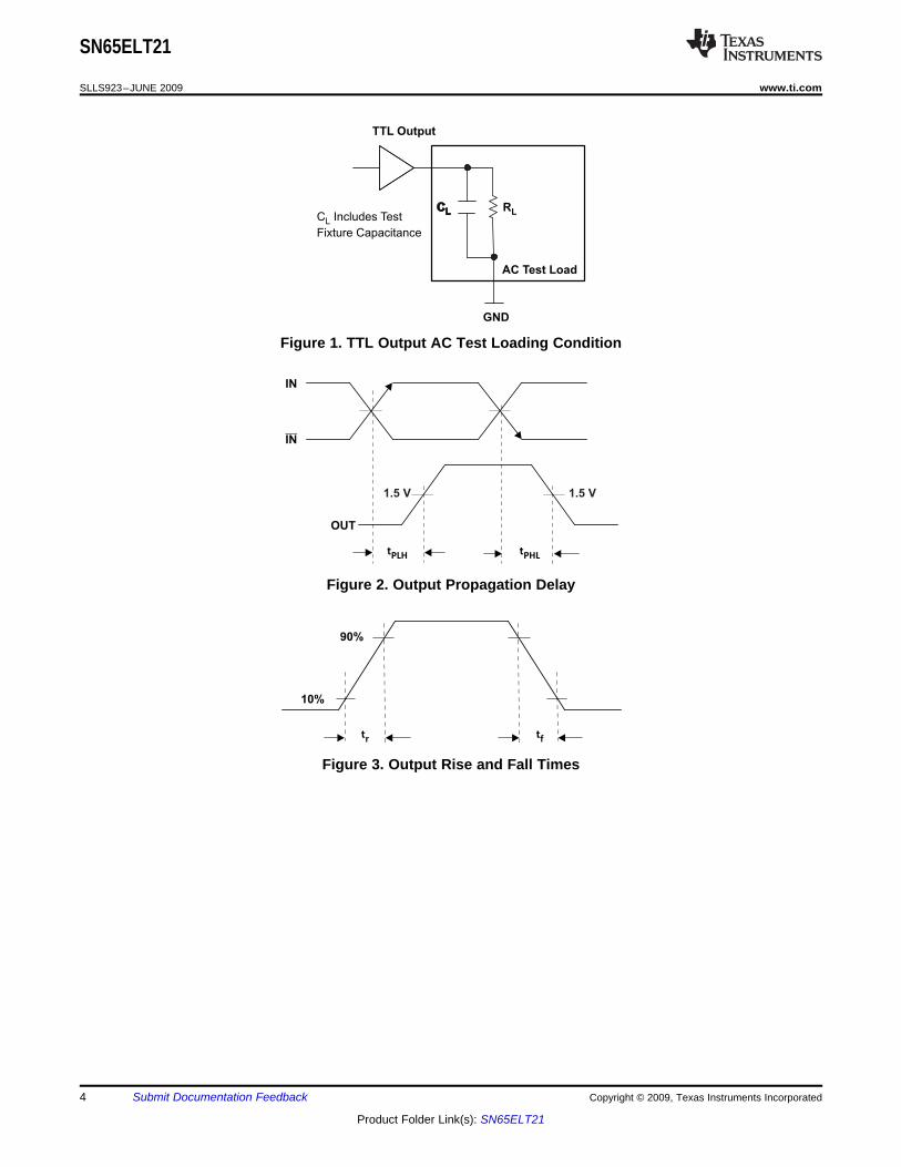
CLC Includes Test
Fixture CapacitanceL
RL
AC Test Load
GND
TTL Output
IN
IN
tPLH
tPHL
OUT
1.5 V1.5 V
90%
10%
tr
tf
SN65ELT21
SLLS923–JUNE 2009....................................................................................................................................................................................................... www.ti.com
Figure 1. TTL Output AC Test Loading Condition
Figure 2. Output Propagation Delay
Figure 3. Output Rise and Fall Times
4 Submit Documentation Feedback Copyright © 2009, Texas Instruments Incorporated
Product Folder Link(s): SN65ELT21
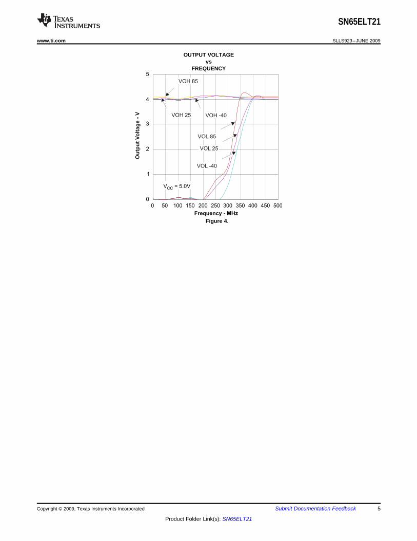
0
1
2
3
4
5
0 50 100 150 200 250 300 350 400 450 500
Frequency - MHz
Ou
tpu
t V
olt
ag
e -
V
VOH 85
VOH 25 VOH -40
VOL 85
VOL 25
VOL -40
V = 5.0VCC
SN65ELT21
www.ti.com ....................................................................................................................................................................................................... SLLS923–JUNE 2009
OUTPUT VOLTAGEvs
FREQUENCY
Figure 4.
Copyright © 2009, Texas Instruments Incorporated Submit Documentation Feedback 5
Product Folder Link(s): SN65ELT21
PACKAGE OPTION ADDENDUM
www.ti.com 11-Apr-2013
Addendum-Page 1
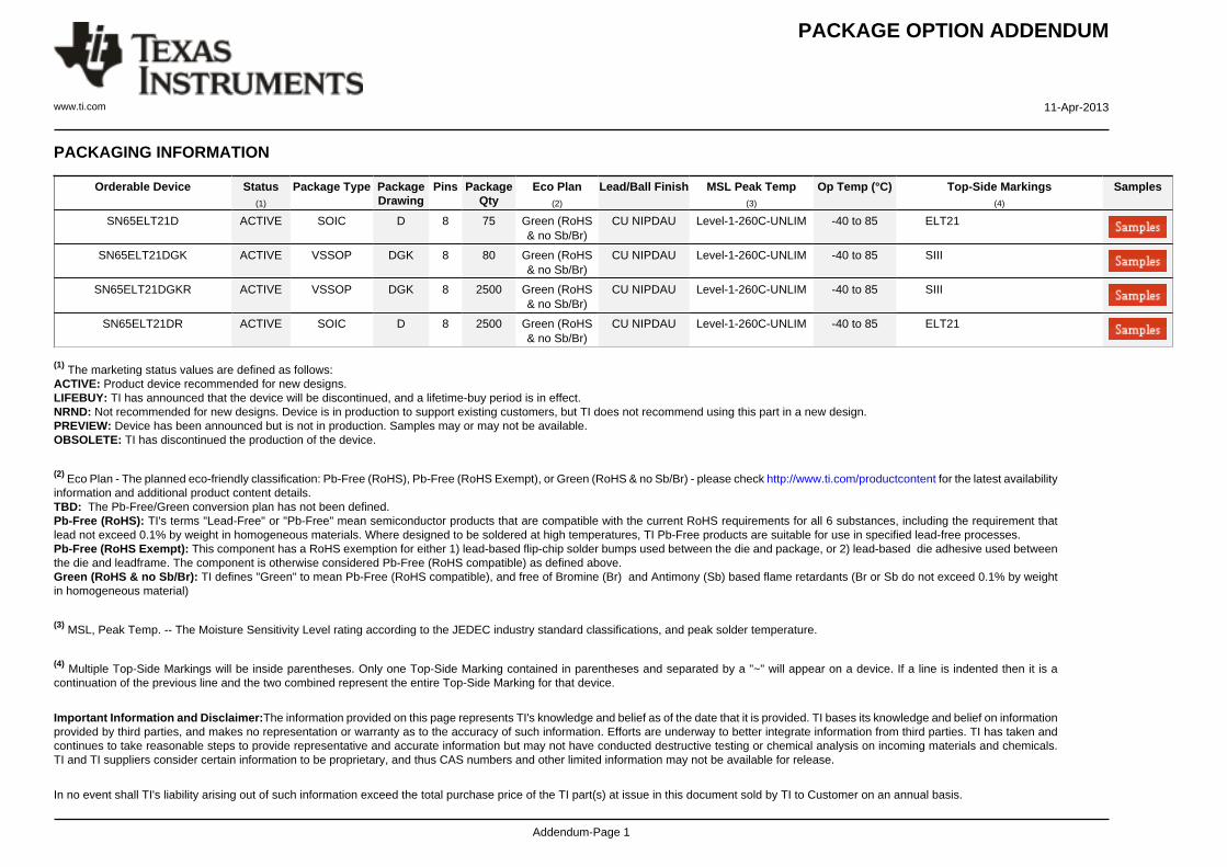
PACKAGING INFORMATION
Orderable Device Status(1)
Package Type PackageDrawing
Pins PackageQty
Eco Plan(2)
Lead/Ball Finish MSL Peak Temp(3)
Op Temp (°C) Top-Side Markings(4)
Samples
SN65ELT21D ACTIVE SOIC D 8 75 Green (RoHS& no Sb/Br)
CU NIPDAU Level-1-260C-UNLIM -40 to 85 ELT21
SN65ELT21DGK ACTIVE VSSOP DGK 8 80 Green (RoHS& no Sb/Br)
CU NIPDAU Level-1-260C-UNLIM -40 to 85 SIII
SN65ELT21DGKR ACTIVE VSSOP DGK 8 2500 Green (RoHS& no Sb/Br)
CU NIPDAU Level-1-260C-UNLIM -40 to 85 SIII
SN65ELT21DR ACTIVE SOIC D 8 2500 Green (RoHS& no Sb/Br)
CU NIPDAU Level-1-260C-UNLIM -40 to 85 ELT21
(1) The marketing status values are defined as follows:ACTIVE: Product device recommended for new designs.LIFEBUY: TI has announced that the device will be discontinued, and a lifetime-buy period is in effect.NRND: Not recommended for new designs. Device is in production to support existing customers, but TI does not recommend using this part in a new design.PREVIEW: Device has been announced but is not in production. Samples may or may not be available.OBSOLETE: TI has discontinued the production of the device.
(2) Eco Plan - The planned eco-friendly classification: Pb-Free (RoHS), Pb-Free (RoHS Exempt), or Green (RoHS & no Sb/Br) - please check http://www.ti.com/productcontent for the latest availabilityinformation and additional product content details.TBD: The Pb-Free/Green conversion plan has not been defined.Pb-Free (RoHS): TI's terms "Lead-Free" or "Pb-Free" mean semiconductor products that are compatible with the current RoHS requirements for all 6 substances, including the requirement thatlead not exceed 0.1% by weight in homogeneous materials. Where designed to be soldered at high temperatures, TI Pb-Free products are suitable for use in specified lead-free processes.Pb-Free (RoHS Exempt): This component has a RoHS exemption for either 1) lead-based flip-chip solder bumps used between the die and package, or 2) lead-based die adhesive used betweenthe die and leadframe. The component is otherwise considered Pb-Free (RoHS compatible) as defined above.Green (RoHS & no Sb/Br): TI defines "Green" to mean Pb-Free (RoHS compatible), and free of Bromine (Br) and Antimony (Sb) based flame retardants (Br or Sb do not exceed 0.1% by weightin homogeneous material)
(3) MSL, Peak Temp. -- The Moisture Sensitivity Level rating according to the JEDEC industry standard classifications, and peak solder temperature.
(4) Multiple Top-Side Markings will be inside parentheses. Only one Top-Side Marking contained in parentheses and separated by a "~" will appear on a device. If a line is indented then it is acontinuation of the previous line and the two combined represent the entire Top-Side Marking for that device.
Important Information and Disclaimer:The information provided on this page represents TI's knowledge and belief as of the date that it is provided. TI bases its knowledge and belief on informationprovided by third parties, and makes no representation or warranty as to the accuracy of such information. Efforts are underway to better integrate information from third parties. TI has taken andcontinues to take reasonable steps to provide representative and accurate information but may not have conducted destructive testing or chemical analysis on incoming materials and chemicals.TI and TI suppliers consider certain information to be proprietary, and thus CAS numbers and other limited information may not be available for release.
In no event shall TI's liability arising out of such information exceed the total purchase price of the TI part(s) at issue in this document sold by TI to Customer on an annual basis.
PACKAGE OPTION ADDENDUM
www.ti.com 11-Apr-2013
Addendum-Page 2
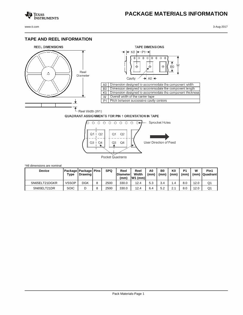
TAPE AND REEL INFORMATION
*All dimensions are nominal
Device PackageType
PackageDrawing
Pins SPQ ReelDiameter
(mm)
ReelWidth
W1 (mm)
A0(mm)
B0(mm)
K0(mm)
P1(mm)
W(mm)
Pin1Quadrant
SN65ELT21DGKR VSSOP DGK 8 2500 330.0 12.4 5.3 3.4 1.4 8.0 12.0 Q1
SN65ELT21DR SOIC D 8 2500 330.0 12.4 6.4 5.2 2.1 8.0 12.0 Q1
PACKAGE MATERIALS INFORMATION
www.ti.com 3-Aug-2017
Pack Materials-Page 1
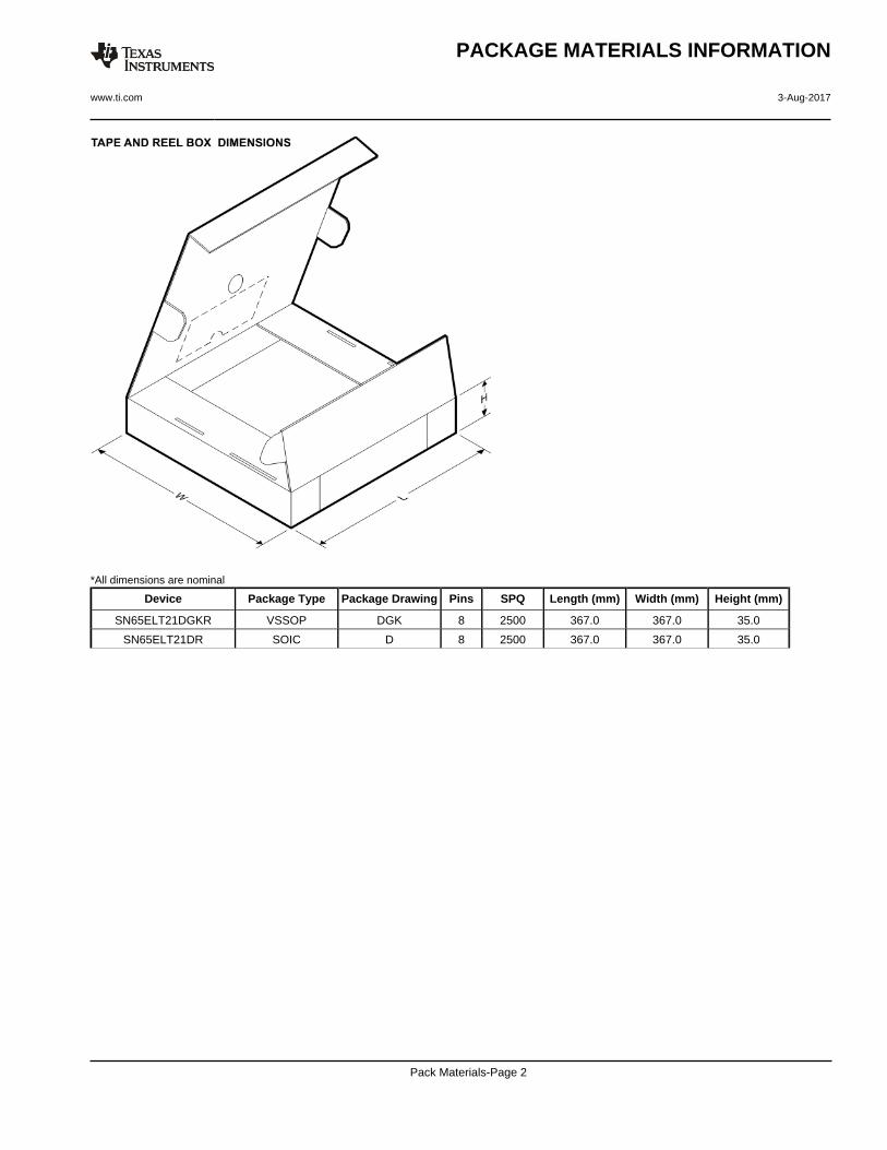
*All dimensions are nominal
Device Package Type Package Drawing Pins SPQ Length (mm) Width (mm) Height (mm)
SN65ELT21DGKR VSSOP DGK 8 2500 367.0 367.0 35.0
SN65ELT21DR SOIC D 8 2500 367.0 367.0 35.0
PACKAGE MATERIALS INFORMATION
www.ti.com 3-Aug-2017
Pack Materials-Page 2
IMPORTANT NOTICE
Texas Instruments Incorporated (TI) reserves the right to make corrections, enhancements, improvements and other changes to itssemiconductor products and services per JESD46, latest issue, and to discontinue any product or service per JESD48, latest issue. Buyersshould obtain the latest relevant information before placing orders and should verify that such information is current and complete.TI’s published terms of sale for semiconductor products (http://www.ti.com/sc/docs/stdterms.htm) apply to the sale of packaged integratedcircuit products that TI has qualified and released to market. Additional terms may apply to the use or sale of other types of TI products andservices.Reproduction of significant portions of TI information in TI data sheets is permissible only if reproduction is without alteration and isaccompanied by all associated warranties, conditions, limitations, and notices. TI is not responsible or liable for such reproduceddocumentation. Information of third parties may be subject to additional restrictions. Resale of TI products or services with statementsdifferent from or beyond the parameters stated by TI for that product or service voids all express and any implied warranties for theassociated TI product or service and is an unfair and deceptive business practice. TI is not responsible or liable for any such statements.Buyers and others who are developing systems that incorporate TI products (collectively, “Designers”) understand and agree that Designersremain responsible for using their independent analysis, evaluation and judgment in designing their applications and that Designers havefull and exclusive responsibility to assure the safety of Designers' applications and compliance of their applications (and of all TI productsused in or for Designers’ applications) with all applicable regulations, laws and other applicable requirements. Designer represents that, withrespect to their applications, Designer has all the necessary expertise to create and implement safeguards that (1) anticipate dangerousconsequences of failures, (2) monitor failures and their consequences, and (3) lessen the likelihood of failures that might cause harm andtake appropriate actions. Designer agrees that prior to using or distributing any applications that include TI products, Designer willthoroughly test such applications and the functionality of such TI products as used in such applications.TI’s provision of technical, application or other design advice, quality characterization, reliability data or other services or information,including, but not limited to, reference designs and materials relating to evaluation modules, (collectively, “TI Resources”) are intended toassist designers who are developing applications that incorporate TI products; by downloading, accessing or using TI Resources in anyway, Designer (individually or, if Designer is acting on behalf of a company, Designer’s company) agrees to use any particular TI Resourcesolely for this purpose and subject to the terms of this Notice.TI’s provision of TI Resources does not expand or otherwise alter TI’s applicable published warranties or warranty disclaimers for TIproducts, and no additional obligations or liabilities arise from TI providing such TI Resources. TI reserves the right to make corrections,enhancements, improvements and other changes to its TI Resources. TI has not conducted any testing other than that specificallydescribed in the published documentation for a particular TI Resource.Designer is authorized to use, copy and modify any individual TI Resource only in connection with the development of applications thatinclude the TI product(s) identified in such TI Resource. NO OTHER LICENSE, EXPRESS OR IMPLIED, BY ESTOPPEL OR OTHERWISETO ANY OTHER TI INTELLECTUAL PROPERTY RIGHT, AND NO LICENSE TO ANY TECHNOLOGY OR INTELLECTUAL PROPERTYRIGHT OF TI OR ANY THIRD PARTY IS GRANTED HEREIN, including but not limited to any patent right, copyright, mask work right, orother intellectual property right relating to any combination, machine, or process in which TI products or services are used. Informationregarding or referencing third-party products or services does not constitute a license to use such products or services, or a warranty orendorsement thereof. Use of TI Resources may require a license from a third party under the patents or other intellectual property of thethird party, or a license from TI under the patents or other intellectual property of TI.TI RESOURCES ARE PROVIDED “AS IS” AND WITH ALL FAULTS. TI DISCLAIMS ALL OTHER WARRANTIES ORREPRESENTATIONS, EXPRESS OR IMPLIED, REGARDING RESOURCES OR USE THEREOF, INCLUDING BUT NOT LIMITED TOACCURACY OR COMPLETENESS, TITLE, ANY EPIDEMIC FAILURE WARRANTY AND ANY IMPLIED WARRANTIES OFMERCHANTABILITY, FITNESS FOR A PARTICULAR PURPOSE, AND NON-INFRINGEMENT OF ANY THIRD PARTY INTELLECTUALPROPERTY RIGHTS. TI SHALL NOT BE LIABLE FOR AND SHALL NOT DEFEND OR INDEMNIFY DESIGNER AGAINST ANY CLAIM,INCLUDING BUT NOT LIMITED TO ANY INFRINGEMENT CLAIM THAT RELATES TO OR IS BASED ON ANY COMBINATION OFPRODUCTS EVEN IF DESCRIBED IN TI RESOURCES OR OTHERWISE. IN NO EVENT SHALL TI BE LIABLE FOR ANY ACTUAL,DIRECT, SPECIAL, COLLATERAL, INDIRECT, PUNITIVE, INCIDENTAL, CONSEQUENTIAL OR EXEMPLARY DAMAGES INCONNECTION WITH OR ARISING OUT OF TI RESOURCES OR USE THEREOF, AND REGARDLESS OF WHETHER TI HAS BEENADVISED OF THE POSSIBILITY OF SUCH DAMAGES.Unless TI has explicitly designated an individual product as meeting the requirements of a particular industry standard (e.g., ISO/TS 16949and ISO 26262), TI is not responsible for any failure to meet such industry standard requirements.Where TI specifically promotes products as facilitating functional safety or as compliant with industry functional safety standards, suchproducts are intended to help enable customers to design and create their own applications that meet applicable functional safety standardsand requirements. Using products in an application does not by itself establish any safety features in the application. Designers mustensure compliance with safety-related requirements and standards applicable to their applications. Designer may not use any TI products inlife-critical medical equipment unless authorized officers of the parties have executed a special contract specifically governing such use.Life-critical medical equipment is medical equipment where failure of such equipment would cause serious bodily injury or death (e.g., lifesupport, pacemakers, defibrillators, heart pumps, neurostimulators, and implantables). Such equipment includes, without limitation, allmedical devices identified by the U.S. Food and Drug Administration as Class III devices and equivalent classifications outside the U.S.TI may expressly designate certain products as completing a particular qualification (e.g., Q100, Military Grade, or Enhanced Product).Designers agree that it has the necessary expertise to select the product with the appropriate qualification designation for their applicationsand that proper product selection is at Designers’ own risk. Designers are solely responsible for compliance with all legal and regulatoryrequirements in connection with such selection.Designer will fully indemnify TI and its representatives against any damages, costs, losses, and/or liabilities arising out of Designer’s non-compliance with the terms and provisions of this Notice.
Mailing Address: Texas Instruments, Post Office Box 655303, Dallas, Texas 75265Copyright © 2017, Texas Instruments Incorporated