Transmission Electron Microscopy Skills:Introduction to transmission electron microscopy
Upload
dr-saad-b-h-faridCategory
view
222download
0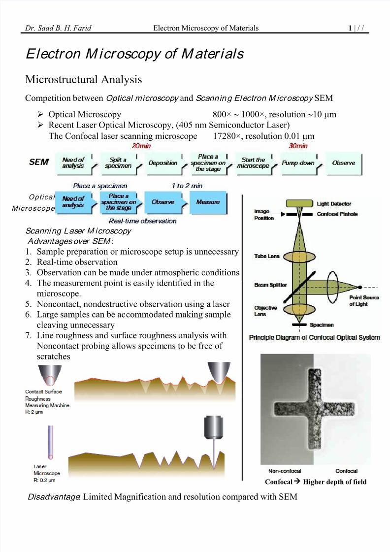
7/27/2019 5- Electron Microscopy of Materials.docx
http://slidepdf.com/reader/full/5-electron-microscopy-of-materialsdocx 1/11
Dr. Saad B. H. Farid Electron Microscopy of Materials 1 | / /
Electron M icroscopy of Mater ials
Microstructural Analysis
Competition between Optical microscopy and Scanning Electron M icroscopy SEM
Optical Microscopy 800× 1000×, resolution 10 m
Recent Laser Optical Microscopy, (405 nm Semiconductor Laser)
The Confocal laser scanning microscope 17280×, resolution 0.01 m
Scanning Laser M icroscopy
Advantages over SEM :1. Sample preparation or microscope setup is unnecessary
2. Real-time observation
3. Observation can be made under atmospheric conditions
4. The measurement point is easily identified in the
microscope.5. Noncontact, nondestructive observation using a laser 6. Large samples can be accommodated making sample
cleaving unnecessary
7. Line roughness and surface roughness analysis with
Noncontact probing allows specimens to be free of
scratches
Disadvantage : Limited Magnification and resolution compared with SEM
Optical
Microscope
Confocal
Higher depth of field
7/27/2019 5- Electron Microscopy of Materials.docx
http://slidepdf.com/reader/full/5-electron-microscopy-of-materialsdocx 2/11
Dr. Saad B. H. Farid Electron Microscopy of Materials 2 | / /
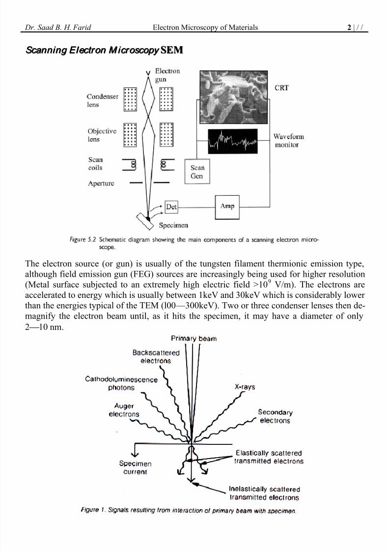
S S c c a a n n n n i i n n g g E E l l e e c c t t r r o o n n M M i i c c r r o o s s c c o o p p y y SSEEMM
The electron source (or gun) is usually of the tungsten filament thermionic emission type,
although field emission gun (FEG) sources are increasingly being used for higher resolution
(Metal surface subjected to an extremely high electric field >109
V/m). The electrons are
accelerated to energy which is usually between 1keV and 30keV which is considerably lower
than the energies typical of the TEM (l00 — 300keV). Two or three condenser lenses then de-
magnify the electron beam until, as it hits the specimen, it may have a diameter of only
2 10 nm.
7/27/2019 5- Electron Microscopy of Materials.docx
http://slidepdf.com/reader/full/5-electron-microscopy-of-materialsdocx 3/11
Dr. Saad B. H. Farid Electron Microscopy of Materials 3 | / /
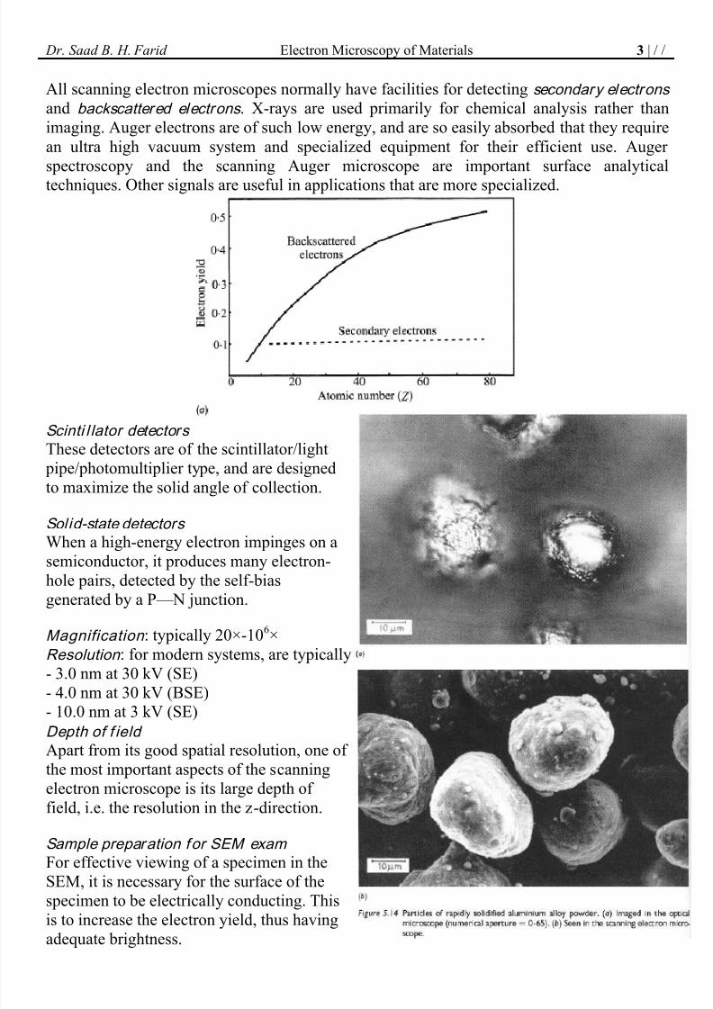
All scanning electron microscopes normally have facilities for detecting secondary electrons
and backscattered electrons . X-rays are used primarily for chemical analysis rather than
imaging. Auger electrons are of such low energy, and are so easily absorbed that they require
an ultra high vacuum system and specialized equipment for their efficient use. Auger
spectroscopy and the scanning Auger microscope are important surface analyticaltechniques. Other signals are useful in applications that are more specialized.
Scinti l lator detectors
These detectors are of the scintillator/light
pipe/photomultiplier type, and are designed
to maximize the solid angle of collection.
Solid-state detectors When a high-energy electron impinges on a
semiconductor, it produces many electron-
hole pairs, detected by the self-bias
generated by a P — N junction.
Magnification : typically 20×-106×
Resolution : for modern systems, are typically
- 3.0 nm at 30 kV (SE)
- 4.0 nm at 30 kV (BSE)
- 10.0 nm at 3 kV (SE)Depth of f ield
Apart from its good spatial resolution, one of
the most important aspects of the scanning
electron microscope is its large depth of
field, i.e. the resolution in the z-direction.
Sample preparation for SEM exam
For effective viewing of a specimen in the
SEM, it is necessary for the surface of thespecimen to be electrically conducting. This
is to increase the electron yield, thus having
adequate brightness.
7/27/2019 5- Electron Microscopy of Materials.docx
http://slidepdf.com/reader/full/5-electron-microscopy-of-materialsdocx 4/11
Dr. Saad B. H. Farid Electron Microscopy of Materials 4 | / /
Few nanometers coating with gold is a general experience to make the sample surface
conductive.
The examination of non-conducting specimens, particularly polymers and biological
materials in the SEM may present other problems, such as specimen degradation by beam
heating, radiation damage, and specimen volatility in the high vacuum. Thus, specialtechniques should be learned by the researcher/technician to overcome this difficulty.
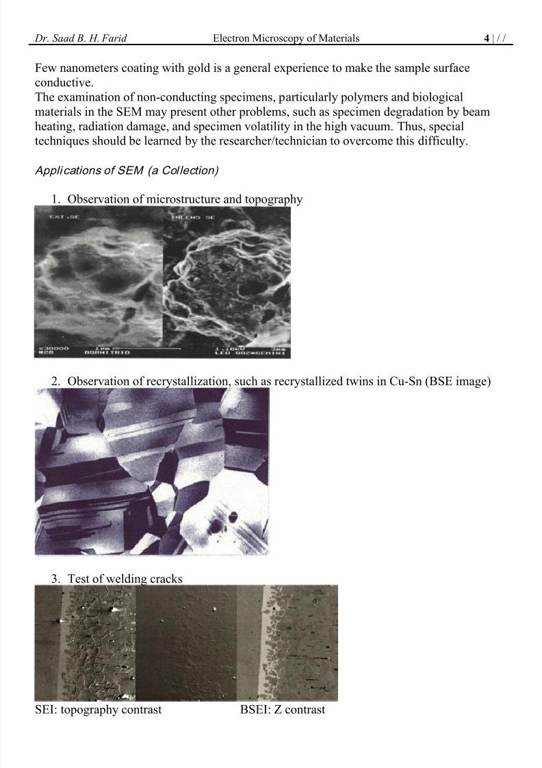
Appli cations of SEM (a Collection)
1. Observation of microstructure and topography
2. Observation of recrystallization, such as recrystallized twins in Cu-Sn (BSE image)
3. Test of welding cracks
SEI: topography contrast BSEI: Z contrast
7/27/2019 5- Electron Microscopy of Materials.docx
http://slidepdf.com/reader/full/5-electron-microscopy-of-materialsdocx 5/11
Dr. Saad B. H. Farid Electron Microscopy of Materials 5 | / /
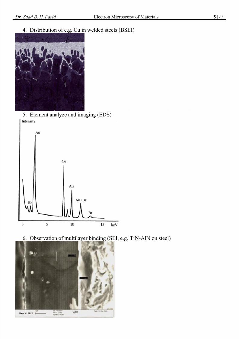
4. Distribution of e.g. Cu in welded steels (BSEI)
5. Element analyze and imaging (EDS)
6. Observation of multilayer binding (SEI, e.g. TiN-AlN on steel)
7/27/2019 5- Electron Microscopy of Materials.docx
http://slidepdf.com/reader/full/5-electron-microscopy-of-materialsdocx 6/11
Dr. Saad B. H. Farid Electron Microscopy of Materials 6 | / /
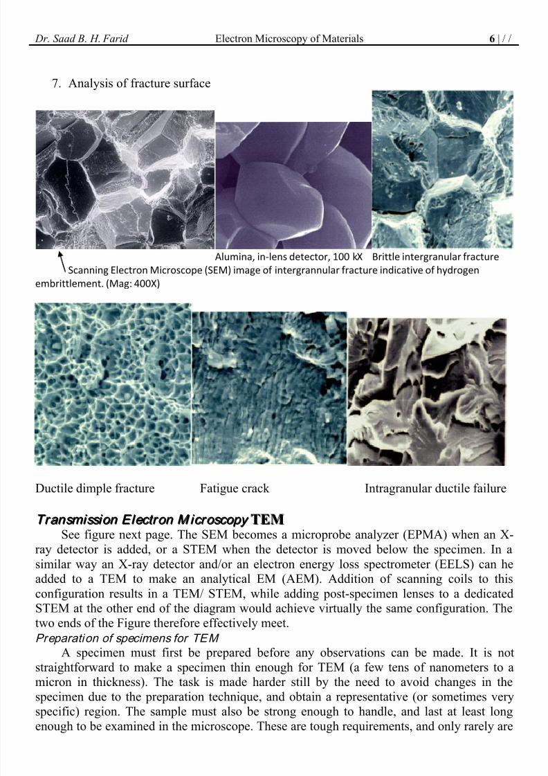
7. Analysis of fracture surface
Alumina, in-lens detector, 100 kX Brittle intergranular fracture
Scanning Electron Microscope (SEM) image of intergrannular fracture indicative of hydrogenembrittlement. (Mag: 400X)
Ductile dimple fracture Fatigue crack Intragranular ductile failure
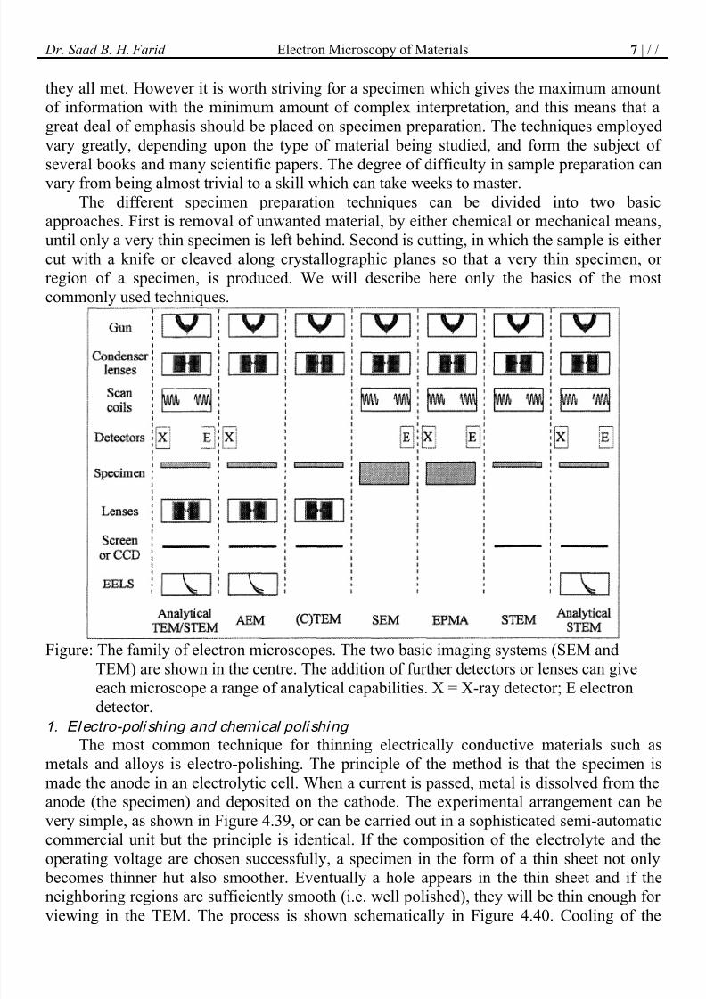
T T r r a a n n s s m m i i s s s s i i o o n n E E l l e e c c t t r r o o n n M M i i c c r r o o s s c c o o p p y y TTEEMM See figure next page. The SEM becomes a microprobe analyzer (EPMA) when an X-
ray detector is added, or a STEM when the detector is moved below the specimen. In a
similar way an X-ray detector and/or an electron energy loss spectrometer (EELS) can headded to a TEM to make an analytical EM (AEM). Addition of scanning coils to this
configuration results in a TEM/ STEM, while adding post-specimen lenses to a dedicatedSTEM at the other end of the diagram would achieve virtually the same configuration. The
two ends of the Figure therefore effectively meet.
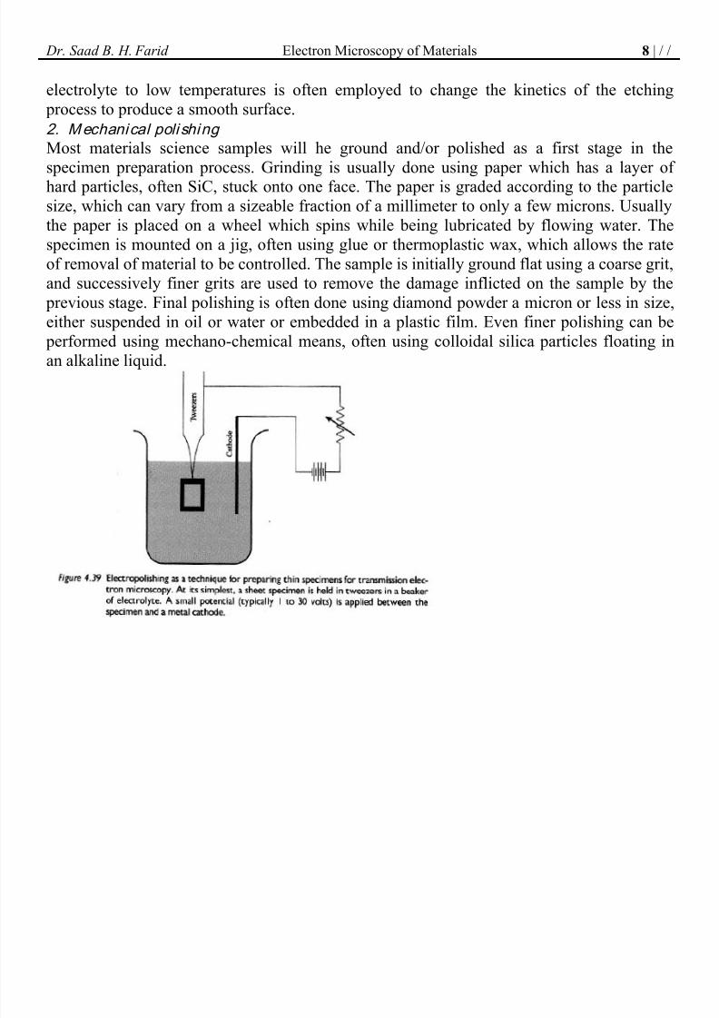
Preparation of specimens for TEM
A specimen must first be prepared before any observations can be made. It is not
straightforward to make a specimen thin enough for TEM (a few tens of nanometers to a
micron in thickness). The task is made harder still by the need to avoid changes in thespecimen due to the preparation technique, and obtain a representative (or sometimes very
specific) region. The sample must also be strong enough to handle, and last at least long
enough to be examined in the microscope. These are tough requirements, and only rarely are
7/27/2019 5- Electron Microscopy of Materials.docx
http://slidepdf.com/reader/full/5-electron-microscopy-of-materialsdocx 7/11
7/27/2019 5- Electron Microscopy of Materials.docx
http://slidepdf.com/reader/full/5-electron-microscopy-of-materialsdocx 8/11
Dr. Saad B. H. Farid Electron Microscopy of Materials 8 | / /
electrolyte to low temperatures is often employed to change the kinetics of the etching
process to produce a smooth surface.
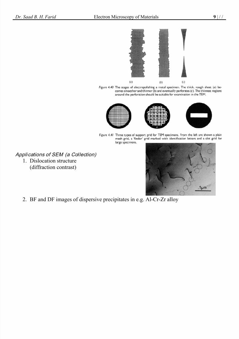
2. Mechanical poli shing
Most materials science samples will he ground and/or polished as a first stage in the
specimen preparation process. Grinding is usually done using paper which has a layer of hard particles, often SiC, stuck onto one face. The paper is graded according to the particle
size, which can vary from a sizeable fraction of a millimeter to only a few microns. Usually
the paper is placed on a wheel which spins while being lubricated by flowing water. The
specimen is mounted on a jig, often using glue or thermoplastic wax, which allows the rate
of removal of material to be controlled. The sample is initially ground flat using a coarse grit,
and successively finer grits are used to remove the damage inflicted on the sample by the
previous stage. Final polishing is often done using diamond powder a micron or less in size,
either suspended in oil or water or embedded in a plastic film. Even finer polishing can be
performed using mechano-chemical means, often using colloidal silica particles floating in
an alkaline liquid.
7/27/2019 5- Electron Microscopy of Materials.docx
http://slidepdf.com/reader/full/5-electron-microscopy-of-materialsdocx 9/11
Dr. Saad B. H. Farid Electron Microscopy of Materials 9 | / /
Appli cations of SEM (a Collection)
1. Dislocation structure
(diffraction contrast)
2. BF and DF images of dispersive precipitates in e.g. Al-Cr-Zr alloy

7/27/2019 5- Electron Microscopy of Materials.docx
http://slidepdf.com/reader/full/5-electron-microscopy-of-materialsdocx 10/11
Dr. Saad B. H. Farid Electron Microscopy of Materials 10 | / /
3. Observation of Organics
This meets versatile medical, biological pharmacological and other applications.
4. HR (high resolution) image of phase in Al alloys
Bright Field BF
Dark Field DF
7/27/2019 5- Electron Microscopy of Materials.docx
http://slidepdf.com/reader/full/5-electron-microscopy-of-materialsdocx 11/11
Dr. Saad B. H. Farid Electron Microscopy of Materials 11 | / /
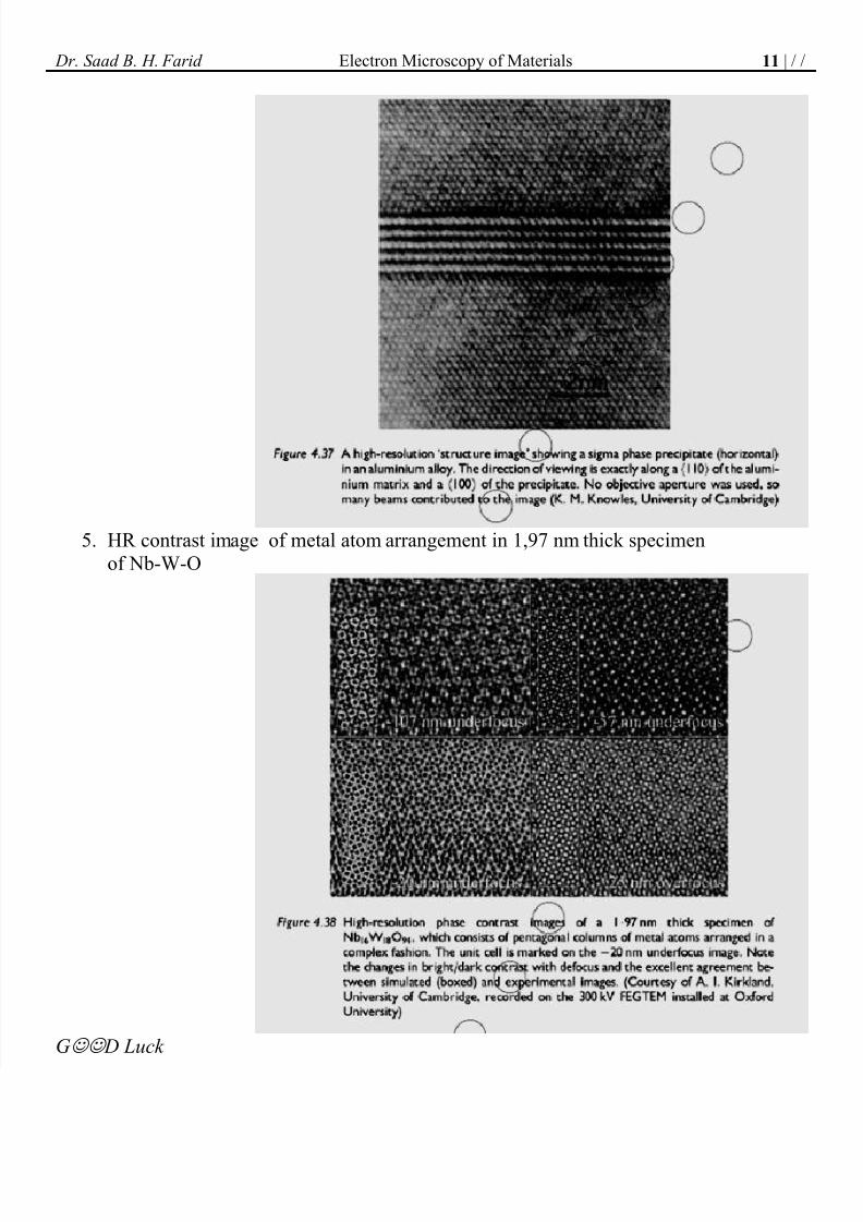
5. HR contrast image of metal atom arrangement in 1,97 nm thick specimen
of Nb-W-O
G D Luck