4774 IEEE TRANSACTIONS ON MICROWAVE THEORY AND …
15
4774 IEEE TRANSACTIONS ON MICROWAVE THEORY AND TECHNIQUES, VOL. 64, NO. 12, DECEMBER 2016 Pulse Shaping: The Missing Piece of Backscatter Radio and RFID John Kimionis, Student Member, IEEE, and Manos M. Tentzeris, Fellow, IEEE Abstract— The increasing use of backscatter radio for pervasive Internet-of-Things systems as a low-power and low-cost communication scheme will result in dense deployments of tags that need to operate under bandwidth (BW) constraints. Typical backscatter tags and computational radio frequency (RF) iden- tification systems are unnecessarily limited to modulating data with “ON–OFF” switching front-ends, which leads to extensive spectrum occupancy, due to the rectangular pulses. This paper sets the foundations to overcome these limitations and proposes designs of RF front-ends that are capable of varying the tag reflection coefficient in a continuous way over time. Arbitrary waveforms can be generated to perform pulse shaping on the backscattered signals, which require significantly reduced BW. The principles presented in this paper will enable sophisticated tags to perform complex modulation schemes under BW con- straints, while maintaining a very low RF front-end complexity, using a single nonlinear component such as a p-i-n diode or field-effect transistor. Migrating the idea of pulse shaping from complex power-demanding active radios to such minimal RF front-ends will complete backscatter radio as a communication scheme for simple RF tags and sensors in large-scale deploy- ments. Each tag becomes a miniature software-defined radio that implements diverse communication schemes with increased spectral efficiency. Index Terms— Backscatter radio, modulation, pulse shap- ing, radio frequency (RF) front-end, RF identification (RFID), software-defined radio (SDR), spectral efficiency. I. I NTRODUCTION I N DENSE backscatter sensor or radio frequency identi- fication (RFID) tag deployments, minimizing the utilized bandwidth (BW) per tag is required to fit a large number of sensors in a dedicated frequency band and also guar- antee low out-of-band interference for regulatory reasons. Each tag’s backscattered signal spectrum has to decay fast with regard to frequency so that the signal’s harmonics are suppressed and do not interfere with nearby sensors, without compromising the signal detection performance. Active radio systems typically utilize pulse shaping techniques to modify the waveform characteristics of the transmitted signals and Manuscript received July 1, 2016; revised October 10, 2016; accepted October 25, 2016. Date of publication November 23, 2016; date of current version December 7, 2016. This work was supported in part by the National Science Foundation-EFRI and in part by the Defense Threat Reduction Agency (DTRA). An earlier version of this paper was presented at the IEEE MTT-S International Microwave Symposium, San Francisco, CA, USA, May 22–27, 2016. The authors are with the School of Electrical and Computer Engineer- ing, Georgia Institute of Technology, Atlanta, GA 30332 USA (e-mail: [email protected]; [email protected]). Color versions of one or more of the figures in this paper are available online at http://ieeexplore.ieee.org. Digital Object Identifier 10.1109/TMTT.2016.2623703 adapt them according to the requirements of BW, data rate, and so on [1], [2]. Although conventional radio utilizes complex electronic components to achieve shaping, backscatter radio typically utilizes minimal RF front-ends consisting of only one or a few nonlinear devices (switches, transistors, and diodes) that switch between discrete states [3]. However, this should not be a strongly limiting factor for getting away from con- ventional ON–OFF keying (OOK) modulation on sophisticated sensing RFID tags that already employ computational units, such as microcontroller units (MCUs), at the core of their system. Examples of such computation-enabled tags include: 1) [4] where an MCU-based tag is built that implements the Gen2 industrial RFID protocol [5]; 2) [6], [7] where MCU-based tags are built to implement custom backscatter communication schemes including OOK and frequency-shift keying (FSK) in nonconventional long-range bistatic archi- tectures presented in [8] and [9]; 3) [10] where MCU-based tags are used in a special case of bistatic architecture named ambient backscatter; 4) [11], [12] where tags are built that exploit multiple load values and RF multiplexers to achieve high-order modulation constellations; and 5) [13] where an MCU tag is operating in harmonic mode to backscatter data at the second harmonic of the reader signal. All these examples utilize rectangular pulses for backscatter communication and thus require extended BW. The work in [14] first demonstrated the feasibility of generating nonrectangular waveforms with a backscatter tag RF front-end comprising a single nonlinear component, by exploiting a continuous variation of the antenna load instead of switching between two discrete values, as in typical backscatter/RFID tags. Appropriate nonlinear compo- nents include diodes, field-effect transistors (FETs), and any other components that feature a voltage-controlled or current- controlled impedance characteristic. Such components are widely used and are available in either discrete semiconductor packages, or they can be implemented on integrated circuit (IC) dies [15]. Although other works in the field of backscatter radio/RFID have included components that are capable of varying impedance, they have not exploited the characteristic of continuous load modulation; instead, they have limited the operation to discrete states and rectangular pulses. Examples include [16], where p-i-n diodes have been utilized for com- munication, and [17], where photo diodes have been utilized for sensing. In the first example, the p-i-n diodes are biased with discrete current levels for a certain duration (symbol period), and therefore the backscatter pulses have a rectangular 0018-9480 © 2016 IEEE. Personal use is permitted, but republication/redistribution requires IEEE permission. See http://www.ieee.org/publications_standards/publications/rights/index.html for more information.
Transcript of 4774 IEEE TRANSACTIONS ON MICROWAVE THEORY AND …

4774 IEEE TRANSACTIONS ON MICROWAVE THEORY AND TECHNIQUES, VOL. 64, NO. 12, DECEMBER 2016
Pulse Shaping: The Missing Piece ofBackscatter Radio and RFID
John Kimionis, Student Member, IEEE, and Manos M. Tentzeris, Fellow, IEEE
Abstract— The increasing use of backscatter radio forpervasive Internet-of-Things systems as a low-power and low-costcommunication scheme will result in dense deployments of tagsthat need to operate under bandwidth (BW) constraints. Typicalbackscatter tags and computational radio frequency (RF) iden-tification systems are unnecessarily limited to modulating datawith “ON–OFF” switching front-ends, which leads to extensivespectrum occupancy, due to the rectangular pulses. This papersets the foundations to overcome these limitations and proposesdesigns of RF front-ends that are capable of varying the tagreflection coefficient in a continuous way over time. Arbitrarywaveforms can be generated to perform pulse shaping on thebackscattered signals, which require significantly reduced BW.The principles presented in this paper will enable sophisticatedtags to perform complex modulation schemes under BW con-straints, while maintaining a very low RF front-end complexity,using a single nonlinear component such as a p-i-n diode orfield-effect transistor. Migrating the idea of pulse shaping fromcomplex power-demanding active radios to such minimal RFfront-ends will complete backscatter radio as a communicationscheme for simple RF tags and sensors in large-scale deploy-ments. Each tag becomes a miniature software-defined radiothat implements diverse communication schemes with increasedspectral efficiency.
Index Terms— Backscatter radio, modulation, pulse shap-ing, radio frequency (RF) front-end, RF identification (RFID),software-defined radio (SDR), spectral efficiency.
I. INTRODUCTION
IN DENSE backscatter sensor or radio frequency identi-fication (RFID) tag deployments, minimizing the utilized
bandwidth (BW) per tag is required to fit a large numberof sensors in a dedicated frequency band and also guar-antee low out-of-band interference for regulatory reasons.Each tag’s backscattered signal spectrum has to decay fastwith regard to frequency so that the signal’s harmonics aresuppressed and do not interfere with nearby sensors, withoutcompromising the signal detection performance. Active radiosystems typically utilize pulse shaping techniques to modifythe waveform characteristics of the transmitted signals and
Manuscript received July 1, 2016; revised October 10, 2016; acceptedOctober 25, 2016. Date of publication November 23, 2016; date of currentversion December 7, 2016. This work was supported in part by the NationalScience Foundation-EFRI and in part by the Defense Threat ReductionAgency (DTRA). An earlier version of this paper was presented at theIEEE MTT-S International Microwave Symposium, San Francisco, CA,USA, May 22–27, 2016.
The authors are with the School of Electrical and Computer Engineer-ing, Georgia Institute of Technology, Atlanta, GA 30332 USA (e-mail:[email protected]; [email protected]).
Color versions of one or more of the figures in this paper are availableonline at http://ieeexplore.ieee.org.
Digital Object Identifier 10.1109/TMTT.2016.2623703
adapt them according to the requirements of BW, data rate, andso on [1], [2]. Although conventional radio utilizes complexelectronic components to achieve shaping, backscatter radiotypically utilizes minimal RF front-ends consisting of only oneor a few nonlinear devices (switches, transistors, and diodes)that switch between discrete states [3]. However, this shouldnot be a strongly limiting factor for getting away from con-ventional ON–OFF keying (OOK) modulation on sophisticatedsensing RFID tags that already employ computational units,such as microcontroller units (MCUs), at the core of theirsystem. Examples of such computation-enabled tags include:1) [4] where an MCU-based tag is built that implementsthe Gen2 industrial RFID protocol [5]; 2) [6], [7] whereMCU-based tags are built to implement custom backscattercommunication schemes including OOK and frequency-shiftkeying (FSK) in nonconventional long-range bistatic archi-tectures presented in [8] and [9]; 3) [10] where MCU-basedtags are used in a special case of bistatic architecture namedambient backscatter; 4) [11], [12] where tags are built thatexploit multiple load values and RF multiplexers to achievehigh-order modulation constellations; and 5) [13] where anMCU tag is operating in harmonic mode to backscatter dataat the second harmonic of the reader signal. All these examplesutilize rectangular pulses for backscatter communication andthus require extended BW.
The work in [14] first demonstrated the feasibility ofgenerating nonrectangular waveforms with a backscatter tagRF front-end comprising a single nonlinear component,by exploiting a continuous variation of the antenna loadinstead of switching between two discrete values, as intypical backscatter/RFID tags. Appropriate nonlinear compo-nents include diodes, field-effect transistors (FETs), and anyother components that feature a voltage-controlled or current-controlled impedance characteristic. Such components arewidely used and are available in either discrete semiconductorpackages, or they can be implemented on integratedcircuit (IC) dies [15].
Although other works in the field of backscatter radio/RFIDhave included components that are capable of varyingimpedance, they have not exploited the characteristic ofcontinuous load modulation; instead, they have limited theoperation to discrete states and rectangular pulses. Examplesinclude [16], where p-i-n diodes have been utilized for com-munication, and [17], where photo diodes have been utilizedfor sensing. In the first example, the p-i-n diodes are biasedwith discrete current levels for a certain duration (symbolperiod), and therefore the backscatter pulses have a rectangular
0018-9480 © 2016 IEEE. Personal use is permitted, but republication/redistribution requires IEEE permission.See http://www.ieee.org/publications_standards/publications/rights/index.html for more information.
KIMIONIS AND TENTZERIS: PULSE SHAPING: MISSING PIECE OF BACKSCATTER RADIO AND RFID 4775
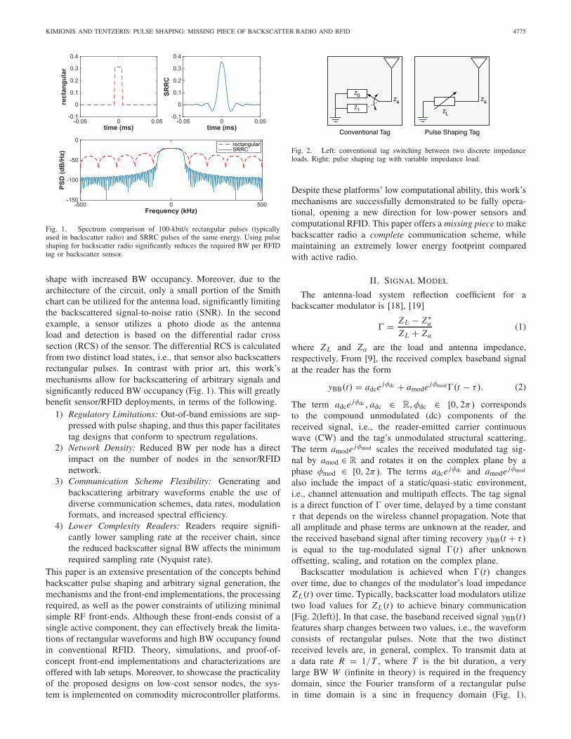
Fig. 1. Spectrum comparison of 100-kbit/s rectangular pulses (typicallyused in backscatter radio) and SRRC pulses of the same energy. Using pulseshaping for backscatter radio significantly reduces the required BW per RFIDtag or backscatter sensor.
shape with increased BW occupancy. Moreover, due to thearchitecture of the circuit, only a small portion of the Smithchart can be utilized for the antenna load, significantly limitingthe backscattered signal-to-noise ratio (SNR). In the secondexample, a sensor utilizes a photo diode as the antennaload and detection is based on the differential radar crosssection (RCS) of the sensor. The differential RCS is calculatedfrom two distinct load states, i.e., that sensor also backscattersrectangular pulses. In contrast with prior art, this work’smechanisms allow for backscattering of arbitrary signals andsignificantly reduced BW occupancy (Fig. 1). This will greatlybenefit sensor/RFID deployments, in terms of the following.
1) Regulatory Limitations: Out-of-band emissions are sup-pressed with pulse shaping, and thus this paper facilitatestag designs that conform to spectrum regulations.
2) Network Density: Reduced BW per node has a directimpact on the number of nodes in the sensor/RFIDnetwork.
3) Communication Scheme Flexibility: Generating andbackscattering arbitrary waveforms enable the use ofdiverse communication schemes, data rates, modulationformats, and increased spectral efficiency.
4) Lower Complexity Readers: Readers require signifi-cantly lower sampling rate at the receiver chain, sincethe reduced backscatter signal BW affects the minimumrequired sampling rate (Nyquist rate).
This paper is an extensive presentation of the concepts behindbackscatter pulse shaping and arbitrary signal generation, themechanisms and the front-end implementations, the processingrequired, as well as the power constraints of utilizing minimalsimple RF front-ends. Although these front-ends consist of asingle active component, they can effectively break the limita-tions of rectangular waveforms and high BW occupancy foundin conventional RFID. Theory, simulations, and proof-of-concept front-end implementations and characterizations areoffered with lab setups. Moreover, to showcase the practicalityof the proposed designs on low-cost sensor nodes, the sys-tem is implemented on commodity microcontroller platforms.
Fig. 2. Left: conventional tag switching between two discrete impedanceloads. Right: pulse shaping tag with variable impedance load.
Despite these platforms’ low computational ability, this work’smechanisms are successfully demonstrated to be fully opera-tional, opening a new direction for low-power sensors andcomputational RFID. This paper offers a missing piece to makebackscatter radio a complete communication scheme, whilemaintaining an extremely lower energy footprint comparedwith active radio.
II. SIGNAL MODEL
The antenna-load system reflection coefficient for abackscatter modulator is [18], [19]
� = Z L − Z∗a
Z L + Za(1)
where Z L and Za are the load and antenna impedance,respectively. From [9], the received complex baseband signalat the reader has the form
yBB(t) = adce jφdc + amode jφmod�(t − τ ). (2)
The term adce jφdc, adc ∈ R, φdc ∈ [0, 2π) correspondsto the compound unmodulated (dc) components of thereceived signal, i.e., the reader-emitted carrier continuouswave (CW) and the tag’s unmodulated structural scattering.The term amode jφmod scales the received modulated tag sig-nal by amod ∈ R and rotates it on the complex plane by aphase φmod ∈ [0, 2π). The terms adce jφdc and amode jφmod
also include the impact of a static/quasi-static environment,i.e., channel attenuation and multipath effects. The tag signalis a direct function of � over time, delayed by a time constantτ that depends on the wireless channel propagation. Note thatall amplitude and phase terms are unknown at the reader, andthe received baseband signal after timing recovery yBB(t + τ )is equal to the tag-modulated signal �(t) after unknownoffsetting, scaling, and rotation on the complex plane.
Backscatter modulation is achieved when �(t) changesover time, due to changes of the modulator’s load impedanceZ L(t) over time. Typically, backscatter load modulators utilizetwo load values for Z L(t) to achieve binary communication[Fig. 2(left)]. In that case, the baseband received signal yBB(t)features sharp changes between two values, i.e., the waveformconsists of rectangular pulses. Note that the two distinctreceived levels are, in general, complex. To transmit data ata data rate R = 1/T , where T is the bit duration, a verylarge BW W (infinite in theory) is required in the frequencydomain, since the Fourier transform of a rectangular pulsein time domain is a sinc in frequency domain (Fig. 1).

4776 IEEE TRANSACTIONS ON MICROWAVE THEORY AND TECHNIQUES, VOL. 64, NO. 12, DECEMBER 2016
However, according to the Nyquist intersymbol interfer-ence (ISI) criterion in communication theory, the required BWcould be minimized to W = R while maintaining reliablecommunication without ISI, which negatively affects bit detec-tion [1]. A pulse typically used in active radio transceiverswith limited BW is the square root raised cosine (SRRC)pulse, which, at the expense of longer pulse duration, featuresa significantly reduced mainlobe BW [20]. The SRRC extendsfrom t1 = −AT to t2 = AT , where A is the filter delay, incontrary to a rectangular pulse that extends from t1 = −T/2to t2 = T/2 [e.g., compare the pulse duration of a rectangularpulse and an SRRC pulse with A = 5 in Fig. 1(top)]. Thisreduces the required pulse BW 1 to
W = 1 + a
T(3)
where 0 ≤ a ≤ 1 is the roll-off factor that defines howfast the pulse spectrum decays in the frequency domain. Thedifference in spectrum occupancy for rectangular and SRRCpulses of the same energy is apparent in Fig. 1(bottom), wherethe power spectral density (PSD) of the two pulses is shown.Moreover, when using SRRC filters at the receiver to matchfilter incoming SRRC pulses, the result is a raised cosine pulse,which satisfies the Nyquist ISI criterion, i.e., it is ISI free,which increases the bit detection performance. Therefore, itis appealing to be able to generate SRRC pulses or otherarbitrary waveforms with smooth envelopes (e.g., Gaussianpulses [1]) with a simple backscatter front-end to significantlysuppress the signal spectral sidelobes, or generate multilevelwaveforms to achieve amplitude modulation schemes suchas M-ary pulse amplitude modulation, or generate arbitrarywaveforms for other modulation schemes (e.g., sinusoids foranalog frequency modulation or digital FSK). As discussed inthe following sections, this can be achieved without the needof high-complexity electronics, but rather with a single activeelement front-end that continuously varies the antenna load ina continuous way.
III. CONTINUOUS LOAD VARIATION
The principles described in this section can be applied to anyantenna that is complex-valued or real-valued, as well as anyvarying load that is complex-valued or real-valued, accordingto the general form of (1). However, without loss of generality,and to make the quantities easy to visualize, a purely resistiveload Z L = R(Vbias) controlled by a bias voltage Vbias andan antenna impedance Za = 50 � are assumed. Then theantenna-load reflection coefficient is
�(Vbias) = R(Vbias) − 50
R(Vbias) + 50. (4)
and it is a real quantity with 1 ≥ �(Vbias) ≥ −1. Let Vmin be alow voltage level for which �(Vmin) = 1, i.e., the antenna loadacts as an open circuit (R → ∞). Similarly, let Vmax be thevoltage level that turns the load to a short circuit (R = 0 �),i.e., the reflection coefficient is �(Vmax) = −1. Moreover,
1“ BW ” here refers to the RF spectrum BW around the modulation carrier(e.g., 900 MHz). The equivalent baseband spectrum would extend from dc to(1 + a)/(2T ) Hz.
Fig. 3. Reflection coefficient of (4) as a function of bias voltage in linearform and impedance representation.
let V0 be the voltage that minimizes the reflection coefficientmagnitude |�(V0)| = 0, which occurs at R = 50 �.
The reflection coefficient as a function of the bias voltageis shown in Fig. 3 in linear scale and on a Smith chart,where it can be seen that reflection coefficient variations closeto the edges of the Smith chart (high return loss) are more“dense,” in contrast with the ones close to the chart’s center,for equidistant variations of the bias voltage. The gray regionsof the linear graph and the Smith chart correspond to positivereflected signals, and the white regions correspond to negativereflected signals. Assuming an incident RF signal to the load,a positive or negative voltage of any level between −1 and +1can be reflected back by applying the appropriate bias value.2
The reflection coefficient can be decomposed to its magni-tude and phase components as shown in Fig. 4. It can beseen that the reflection coefficient values can be split intoone “positive” region and one “negative” region. Note thatthe point of sharp transition in phase coincides with the pointwhere the reflection coefficient amplitude is minimized. Thisdecomposition is useful because even if there is a phaserotation of �(Vbias), the amplitude function will remain thesame, and the two regions can still be defined, since they willhave opposite signs. The breakpoint can be found by
V0 = arg minVbias
|�(Vbias)|. (5)
Then the positive region will be the �(Vbias) values for whichVbias < V0, and the negative region will be the �(Vbias) values
2The work in [21] has offered designs that backscatter signals with reflectioncoefficient values |�| > 1. Those designs involve negative-resistance loads toamplify-and-reflect incident signals; this paper assumes passive loads only,confined within the unitary circle of the Smith chart.
KIMIONIS AND TENTZERIS: PULSE SHAPING: MISSING PIECE OF BACKSCATTER RADIO AND RFID 4777
Fig. 4. Reflection coefficient of (4) decomposed to magnitude and phasecomponents, defining a positive and a negative reflected signal region.
Fig. 5. Inverted function of (6) providing the required bias voltage to achievea certain reflection coefficient value.
for which Vbias > V0. Even if the definition of the positiveand negative values is inverted, it does not alter the pulseshaping principle, since the opposite phase will just contributean extra π radians in the already-unknown phase at the receiver[φmod in (2)]. After this decomposition, it becomes apparentthat any signal level (from 0 to 1) can be generated withtwo possible signs, making it possible to generate arbitrarywaveforms.
To generate an arbitrary signal, the required bias voltageto yield the corresponding reflection coefficient is needed.This involves inverting the function �(Vbias), i.e., finding thefunction
Vbias(�), for which: �(Vbias(�)) ≡ �(Vbias). (6)
Note that Vbias and � denote scalar values, while Vbias(·) and�(·) denote scalar functions. From Fig. 3(top), it can be seenthat �(Vbias) is a 1–1 function, and thus invertible; the inverseVbias(�) function is shown in Fig. 5.
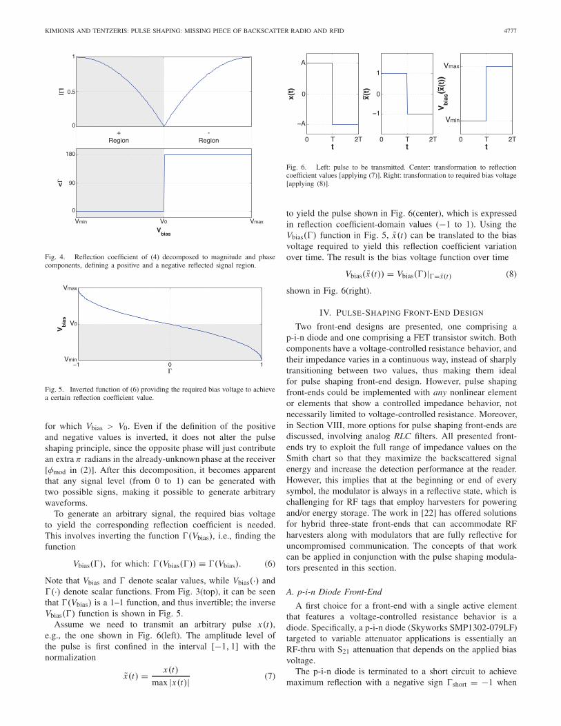
Assume we need to transmit an arbitrary pulse x(t),e.g., the one shown in Fig. 6(left). The amplitude level ofthe pulse is first confined in the interval [−1, 1] with thenormalization
x(t) = x(t)
max |x(t)| (7)
Fig. 6. Left: pulse to be transmitted. Center: transformation to reflectioncoefficient values [applying (7)]. Right: transformation to required bias voltage[applying (8)].
to yield the pulse shown in Fig. 6(center), which is expressedin reflection coefficient-domain values (−1 to 1). Using theVbias(�) function in Fig. 5, x(t) can be translated to the biasvoltage required to yield this reflection coefficient variationover time. The result is the bias voltage function over time
Vbias(x(t)) = Vbias(�)|�=x(t) (8)
shown in Fig. 6(right).
IV. PULSE-SHAPING FRONT-END DESIGN
Two front-end designs are presented, one comprising ap-i-n diode and one comprising a FET transistor switch. Bothcomponents have a voltage-controlled resistance behavior, andtheir impedance varies in a continuous way, instead of sharplytransitioning between two values, thus making them idealfor pulse shaping front-end design. However, pulse shapingfront-ends could be implemented with any nonlinear elementor elements that show a controlled impedance behavior, notnecessarily limited to voltage-controlled resistance. Moreover,in Section VIII, more options for pulse shaping front-ends arediscussed, involving analog RLC filters. All presented front-ends try to exploit the full range of impedance values on theSmith chart so that they maximize the backscattered signalenergy and increase the detection performance at the reader.However, this implies that at the beginning or end of everysymbol, the modulator is always in a reflective state, which ischallenging for RF tags that employ harvesters for poweringand/or energy storage. The work in [22] has offered solutionsfor hybrid three-state front-ends that can accommodate RFharvesters along with modulators that are fully reflective foruncompromised communication. The concepts of that workcan be applied in conjunction with the pulse shaping modula-tors presented in this section.
A. p-i-n Diode Front-End
A first choice for a front-end with a single active elementthat features a voltage-controlled resistance behavior is adiode. Specifically, a p-i-n diode (Skyworks SMP1302-079LF)targeted to variable attenuator applications is essentially anRF-thru with S21 attenuation that depends on the applied biasvoltage.
The p-i-n diode is terminated to a short circuit to achievemaximum reflection with a negative sign �short = −1 when
4778 IEEE TRANSACTIONS ON MICROWAVE THEORY AND TECHNIQUES, VOL. 64, NO. 12, DECEMBER 2016
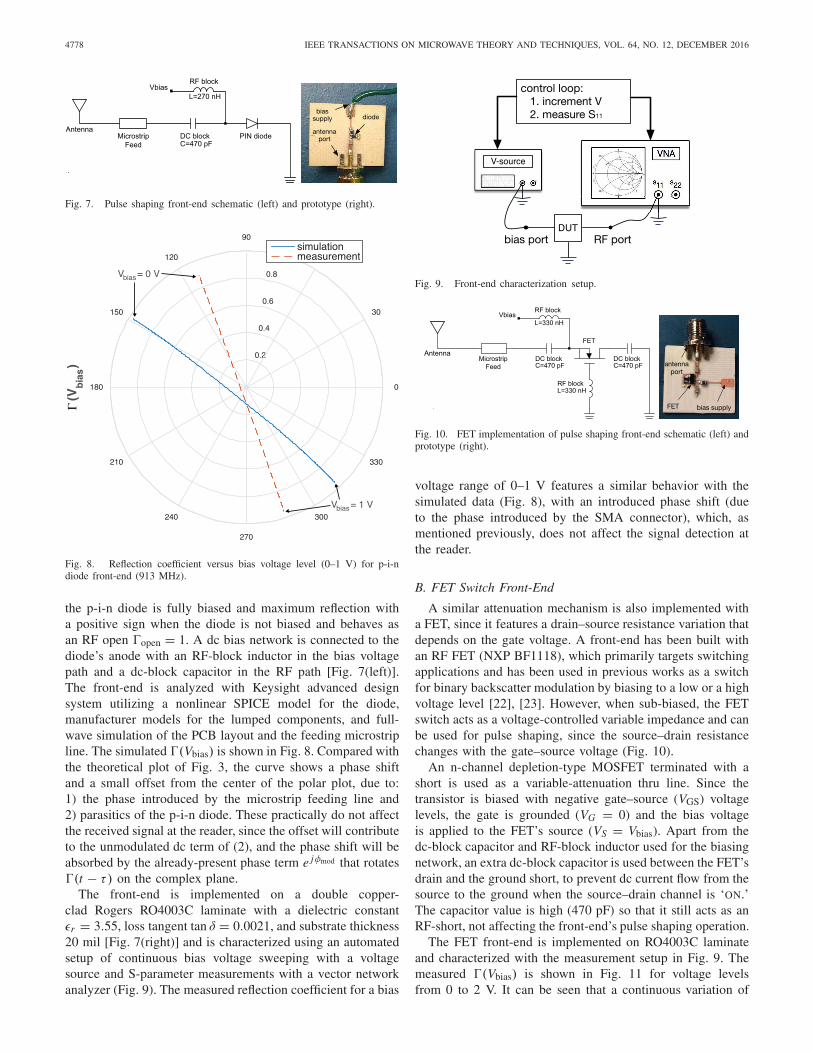
Fig. 7. Pulse shaping front-end schematic (left) and prototype (right).
Fig. 8. Reflection coefficient versus bias voltage level (0–1 V) for p-i-ndiode front-end (913 MHz).
the p-i-n diode is fully biased and maximum reflection witha positive sign when the diode is not biased and behaves asan RF open �open = 1. A dc bias network is connected to thediode’s anode with an RF-block inductor in the bias voltagepath and a dc-block capacitor in the RF path [Fig. 7(left)].The front-end is analyzed with Keysight advanced designsystem utilizing a nonlinear SPICE model for the diode,manufacturer models for the lumped components, and full-wave simulation of the PCB layout and the feeding microstripline. The simulated �(Vbias) is shown in Fig. 8. Compared withthe theoretical plot of Fig. 3, the curve shows a phase shiftand a small offset from the center of the polar plot, due to:1) the phase introduced by the microstrip feeding line and2) parasitics of the p-i-n diode. These practically do not affectthe received signal at the reader, since the offset will contributeto the unmodulated dc term of (2), and the phase shift will beabsorbed by the already-present phase term e jφmod that rotates�(t − τ ) on the complex plane.
The front-end is implemented on a double copper-clad Rogers RO4003C laminate with a dielectric constantεr = 3.55, loss tangent tan δ = 0.0021, and substrate thickness20 mil [Fig. 7(right)] and is characterized using an automatedsetup of continuous bias voltage sweeping with a voltagesource and S-parameter measurements with a vector networkanalyzer (Fig. 9). The measured reflection coefficient for a bias
Fig. 9. Front-end characterization setup.
Fig. 10. FET implementation of pulse shaping front-end schematic (left) andprototype (right).
voltage range of 0–1 V features a similar behavior with thesimulated data (Fig. 8), with an introduced phase shift (dueto the phase introduced by the SMA connector), which, asmentioned previously, does not affect the signal detection atthe reader.
B. FET Switch Front-End
A similar attenuation mechanism is also implemented witha FET, since it features a drain–source resistance variation thatdepends on the gate voltage. A front-end has been built withan RF FET (NXP BF1118), which primarily targets switchingapplications and has been used in previous works as a switchfor binary backscatter modulation by biasing to a low or a highvoltage level [22], [23]. However, when sub-biased, the FETswitch acts as a voltage-controlled variable impedance and canbe used for pulse shaping, since the source–drain resistancechanges with the gate–source voltage (Fig. 10).
An n-channel depletion-type MOSFET terminated with ashort is used as a variable-attenuation thru line. Since thetransistor is biased with negative gate–source (VGS) voltagelevels, the gate is grounded (VG = 0) and the bias voltageis applied to the FET’s source (VS = Vbias). Apart from thedc-block capacitor and RF-block inductor used for the biasingnetwork, an extra dc-block capacitor is used between the FET’sdrain and the ground short, to prevent dc current flow from thesource to the ground when the source–drain channel is ‘ON.’The capacitor value is high (470 pF) so that it still acts as anRF-short, not affecting the front-end’s pulse shaping operation.
The FET front-end is implemented on RO4003C laminateand characterized with the measurement setup in Fig. 9. Themeasured �(Vbias) is shown in Fig. 11 for voltage levelsfrom 0 to 2 V. It can be seen that a continuous variation of
KIMIONIS AND TENTZERIS: PULSE SHAPING: MISSING PIECE OF BACKSCATTER RADIO AND RFID 4779
Fig. 11. Reflection coefficient versus bias voltage level (0–2 V) for FETfront-end (913 MHz).
the reflection coefficient is achieved when changing the biasvoltage, although the reflection coefficient variation does notcover the whole Smith chart from end to end. This is due tothe insertion loss of the FET switch at the “ON” state, andwill affect the backscattered signal in terms of lower reflectedpower. Although there is an offset from the center of the polarplot, a scaling, and a phase shift, these do not affect the signaldemodulation at the reader, and proper processing steps shownin Section V can guarantee the exploitation of the full rangeof reflection coefficient values. Also, the effect of the smallcurvature close to the value Vbias = 0 will be negligible asshown in Section V.
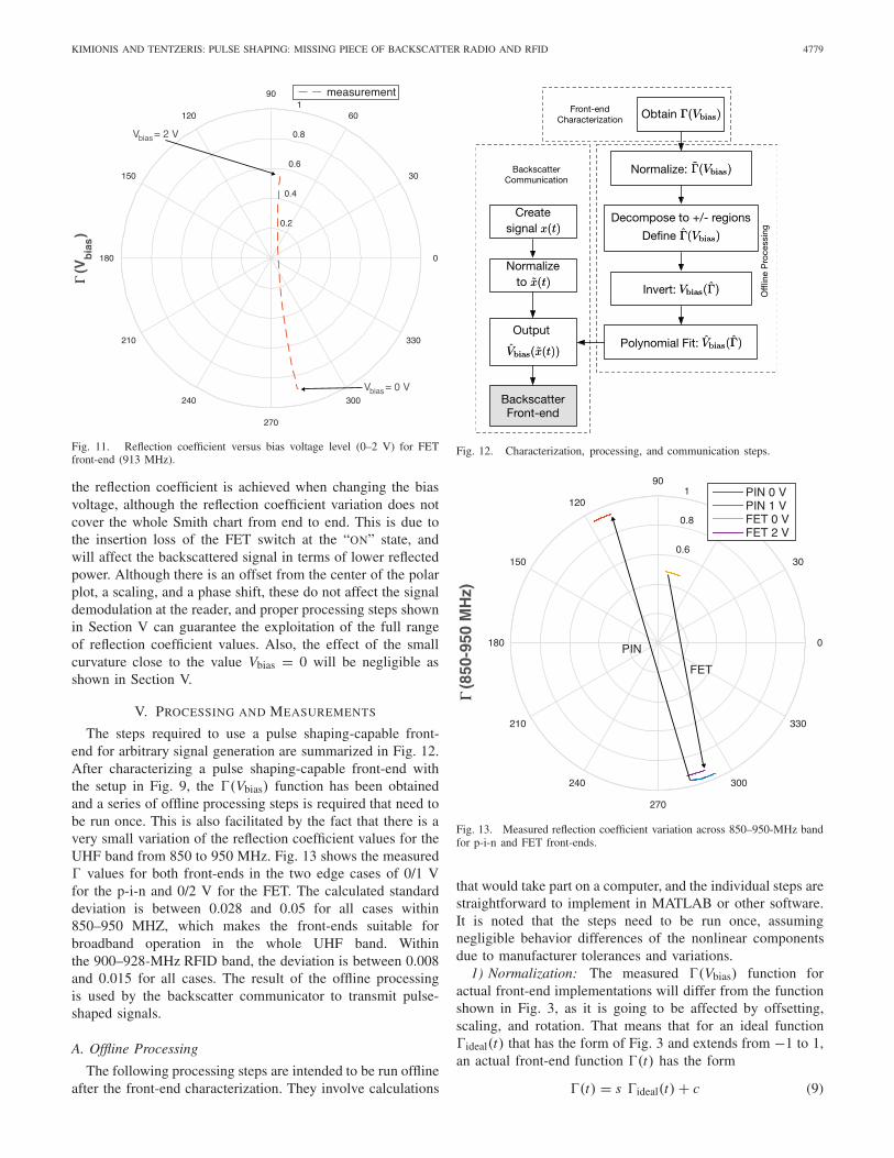
V. PROCESSING AND MEASUREMENTS
The steps required to use a pulse shaping-capable front-end for arbitrary signal generation are summarized in Fig. 12.After characterizing a pulse shaping-capable front-end withthe setup in Fig. 9, the �(Vbias) function has been obtainedand a series of offline processing steps is required that need tobe run once. This is also facilitated by the fact that there is avery small variation of the reflection coefficient values for theUHF band from 850 to 950 MHz. Fig. 13 shows the measured� values for both front-ends in the two edge cases of 0/1 Vfor the p-i-n and 0/2 V for the FET. The calculated standarddeviation is between 0.028 and 0.05 for all cases within850–950 MHZ, which makes the front-ends suitable forbroadband operation in the whole UHF band. Withinthe 900–928-MHz RFID band, the deviation is between 0.008and 0.015 for all cases. The result of the offline processingis used by the backscatter communicator to transmit pulse-shaped signals.
A. Offline Processing
The following processing steps are intended to be run offlineafter the front-end characterization. They involve calculations
Fig. 12. Characterization, processing, and communication steps.
Fig. 13. Measured reflection coefficient variation across 850–950-MHz bandfor p-i-n and FET front-ends.
that would take part on a computer, and the individual steps arestraightforward to implement in MATLAB or other software.It is noted that the steps need to be run once, assumingnegligible behavior differences of the nonlinear componentsdue to manufacturer tolerances and variations.
1) Normalization: The measured �(Vbias) function foractual front-end implementations will differ from the functionshown in Fig. 3, as it is going to be affected by offsetting,scaling, and rotation. That means that for an ideal function�ideal(t) that has the form of Fig. 3 and extends from −1 to 1,an actual front-end function �(t) has the form
�(t) = s �ideal(t) + c (9)

4780 IEEE TRANSACTIONS ON MICROWAVE THEORY AND TECHNIQUES, VOL. 64, NO. 12, DECEMBER 2016
Fig. 14. Normalization of reflection coefficient values. Measured data fromp-i-n diode used for processing.
where s, c ∈ C, i.e., the scaling factor s will scale downand rotate the �ideal(t) function on the complex plane, andthe offset factor c will move the scaled-and-rotated functions�ideal(t) toward any direction on the complex plane. For sucha function, the baseband received signal at the reader will be
yBB(t) = adce jφdc + amode jφmod�(t − τ )
= adce jφdc + amode jφmod(s �ideal(t − τ ) + c)
= a′dce jφ′
dc + a′mode jφ′
mod�ideal(t − τ ) (10)
where a′dce jφ′
dc = adce jφdc+c amode jφmod is the new compoundunmodulated dc term and a′
mode jφ′mod = s amode jφmod is the
scaling and rotating term of the modulated signal �ideal(t −τ ).The signal of (10) is of the same form with (2), since the dcterms and scaling terms are unknown at the reader. Therefore,any offset, scaling, or rotation of the reflection coefficient doesnot affect the reader processing.
Since offsetting, scaling, and rotation do not affect readerprocessing, it is convenient to normalize the measured reflec-tion coefficient values to the form of Fig. 3 so that thesubsequent steps treat reflection coefficient functions for anyfront-end in the same way. The normalization operation is
�(Vbias) = � − c
s= s∗�(Vbias) − s∗c
|s|2 (11)
where c is the offset factor estimate
c = �(Vmax) + �(Vmin)
2(12)
s is the scaling factor estimate
s = �(Vmax) − �(Vmin)
2(13)
and s∗ is the complex conjugate of s. In Fig. 14(top), themeasured reflection coefficient values of the p-i-n front-endcan be seen for bias voltages from 0.4 to 0.82 V. The reasonfor truncating the 0–1 V measurements’ interval to 0.4–0.82 V
Fig. 15. Inverted Vbias(�) function and polynomial-fitted Vbias(�) points.Measured data from p-i-n diode are used for processing.
is that practically any voltage level between 0 and 0.4 V yields� = 0.9 and any level between 0.82 and 1 V practicallyyields � = −0.9. In Fig. 14(bottom), the normalized reflectioncoefficient values for the same voltage interval can be seen.Note how the polar plot and the magnitude of the reflectioncoefficient are of the same form with the theoretical plots(Figs. 3 and 4).
2) Decomposition to Positive and Negative Regions:As discussed in Section III, the reflection coefficient functionis decomposed to a positive and a negative region. Thisinvolves estimating the breakpoint
V0 = arg minVbias
|�(Vbias)| (14)
and then defining the function
�(Vbias) ={
|�(Vbias)|, Vbias ≤ V0
−|�(Vbias)|, Vbias > V0.(15)
3) Function Inversion: The function �(Vbias) with the twopositive/negative regions is 1–1 and is inverted to obtainVbias(�), which can be used as a lookup function to translatesignals in reflection coefficient-domain values (in [−1, 1]) tocorresponding bias voltage levels.
4) Polynomial Fitting: A polynomial fitting step follows,which describes function Vbias(�) with a small number ofcoefficients, and smooths out signal discontinuities and mea-surement noise. The coefficients can be used to store thefunction in a low-memory device such as an MCU for laterevaluation, or evaluate the function in predefined steps of �and store the resulting values in a lookup table. In Fig. 15, theinverted function Vbias(�) is plotted along with its evaluated
polynomial-fit function Vbias(�).
B. Backscatter Communicator
The steps associated with the backscatter communication(Fig. 12) are intended to run real time on a tag that eithergenerates bits based on dynamic information (e.g., sensor data)or recalls static bits from its memory (e.g., identification data).The following steps are intended to run in a loop.

KIMIONIS AND TENTZERIS: PULSE SHAPING: MISSING PIECE OF BACKSCATTER RADIO AND RFID 4781
Fig. 16. Two SRRC pulses (one positive and one negative) in reflectioncoefficient and bias voltage representation. Measured data from p-i-n diodeare used for processing.
Fig. 17. Front-end measurement setup.
1) Signal Creation: The communicator is generating anarbitrary signal x(t) for transmission, e.g., a positive and anegative SRRC pulse in Fig. 16(top).
2) Normalization: The signal x(t) is normalized to x(t)according to (7), to constrain it to reflection coefficient-domainvalues, from −1 to 1.
3) Voltage Output: The fitted function Vbias(�) is used totranslate the signal x(t) to the required voltage levels. Thiscan be done by evaluating a N-degree polynomial with
Vbias(x) = pN x N + pN−1 x N−1 + · · · + p1x + p0 (16)
where pn, n ∈ N are the fitted polynomial coefficientsobtained during the offline processing step B-4 . The signalVbias(x(t)) is output to bias the pulse shaping RF front-end.Fig. 16(bottom) shows the bias voltage levels required tobackscatter the pulses of Fig. 16(top).
VI. PULSE SHAPING MEASUREMENTS
To test the pulse shaping front-ends, the experimental setupin Fig. 17 has been utilized, consisting of a full-duplexsoftware-defined radio (SDR) whose transmit (Tx) and receive(Rx) ports are connected to a UHF circulator and a voltage
Fig. 18. 50-b SRRC-modulated waveform to be backscattered. Top: in reflec-tion coefficient domain. Bottom: translated to bias voltage domain withmeasured p-i-n front-end data.
source that is controlled to output pulse-shaped bitstreams.The front-end is first directly wired to the third circulator portwith an SMA cable. The SDR transmitter chain generatesa CW at 913 MHz that excites the front-end through thecirculator and the response is recorded by the SDR receiverchain. A bitstream of N = 50 b is generated and pulse shapedwith an SRRC pulse with rolloff factor α = 0.5 and filter delayA = 6. The values were selected for moderate mainlobe width(as a increases, the mainlobe becomes wider) and moderatefilter length and sidelobe suppression (as A increases, thepulse becomes longer, but with a larger sidelobe suppres-sion). The pulse train is normalized to the [−1, 1] intervaland is translated to the required bias voltage, using theVbias(�) function (Fig. 18 for the p-i-n front-end). The SDRimplements a receiver with SRRC matched filtering, bit-levelsynchronization, and symbol detection to verify the accuratereception of the bitstream. For wireless measurements, thefront-end is detached from the circulator and is connected to aUHF antenna. The third port of the circulator is also connectedto a UHF antenna for wireless transmission and reception fromthe SDR at the 900-MHz band.
The wireless measurements have been conducted in anoffice environment with heavy multipath and clutter at913 MHz with 2-dBi omnidirectional antennas for the readerand modulator, and carrier transmission power PT = 15 dBm.
For comparison, a front-end consisting of a simple ON–OFF
RF switch is tested with the same bitstream. In Fig. 19(a), thebitstream is shown, modulated with conventional rectangularpulses. In Fig. 19(b) and (c), the SDR-received backscatteredSRRC pulses from the p-i-n front-end are shown for wiredand wireless cases, respectively. The backscattered SRRCpulses are smooth, showcasing the continuity of �(t) achievedwith the p-i-n front-end, and are successfully decoded by theSDR receiver after matched filtering. In Fig. 19(d), the samebitstream with SRRC pulses is shown for the FET front-end.
In Fig. 20, the eye diagrams of the received SRRC wave-forms are shown. The top eye diagram corresponds to an ideal

4782 IEEE TRANSACTIONS ON MICROWAVE THEORY AND TECHNIQUES, VOL. 64, NO. 12, DECEMBER 2016
Fig. 19. SDR -measured backscatter signals in time domain. (a) Conventionalrectangular pulses. (b), (c) SRRC pulses with p-i-n front-end. (d) SRRC pulseswith FET front-end. (e) SRRC pulses with MCU + FET front-end.
(simulated) SRRC pulse train. The middle and bottom eyediagrams correspond to the p-i-n-generated and FET-generatedSRRC pulse trains. It can be seen that the actual front-endbackscattered pulses are closely following the envelope ofthe ideal SRRC pulses. The eye maximum height is equal tothe magnitude of the difference of the reflection coefficientvalues at 0/1 V for the p-i-n front-end and 0/2 V for theFET front-end, respectively. The eye diagram is useful forquantifying the timing errors (jitter) of the pulse-shaped bits.The analyzed jitter percentage for the p-i-n front-end is 0.4%,and for the FET front-end, it is 0.35%. In Fig. 20(bottom),a portion of the SRRC-shaped pulsetrain is overlaid for theideal case and the p-i-n and FET front-ends. It can be seenthat the SRRC envelope is followed with minor variations, andmost importantly, for the FET case, the effect of the curvatureof �(Vbias) (Fig. 11) is negligible and has not affected thepulse shape. This verifies the accurate generation of the SRRCshape, without significant signal distortion.
The spectrum of the received rectangular pulse-modulateddata is shown in Fig. 21 across with the spectrum ofthe SRRC-shaped data with the p-i-n front-end for a datarate of R = 100 kbits/s. It is apparent that the powerdecay is sharper for SRRC pulse-shaped backscatter, with anout-of-band suppression of up to 35 dB, for the same receivedpulse energy. Moreover, the SDR-captured spectrum of the
Fig. 20. Eye diagrams for SRRC pulse transmission and received pulsesoverlay for ideal SRRC, measured p-i-n-generated SRRC, and measured FET-generated SRRC.
SRRC pulse-shaped data occupies a frequency window of150 kHz, which matches with the theoretical BW of SRRCW = (1 + α)R = 150 kHz. It is noted that the spectrumaround the second harmonic of the backscatter signal wasmonitored for reflected harmonics due to nonlinearity effects,but no increased power was observed.
In Fig. 22, the smoothed spectra of rectangular pulses,SRRC pulses from the p-i-n front-end, and SRRC pulses fromthe FET front-end are plotted for easy visual comparison. Thetwo pulse-shaping front-ends feature an equal-width mainlobe,while the sidelobe suppression for the FET front-end is slightlyhigher (up to 42 dB) compared with the p-i-n front-end(up to 37 dB). The mainlobe of the pulse shaping front-ends’signals is narrower than the rectangular pulse one, and sidelobesuppression is around 40 dB with a fast decaying spectrum,

KIMIONIS AND TENTZERIS: PULSE SHAPING: MISSING PIECE OF BACKSCATTER RADIO AND RFID 4783
Fig. 21. Measured spectrum comparison of wireless SDR-received backscat-ter rectangular pulse and SRRC pulse-shaped backscatter. The strong dc peakcorresponds to the reader’s CW that illuminates the backscatter modulator.
Fig. 22. Measured spectrum comparison of rectangular pulse-modulatedwaveform, SRRC pulse-shaped waveform from the p-i-n front-end, SRRCpulse-shaped waveform from the FET front-end, and SRRC pulse-shapedwaveform from the FET driven by an MCU.
in contrast with a maximum suppression of 25 dB for therectangular pulses and a slower decaying spectrum.
VII. FRONT-END ENERGY EFFICIENCY
Backscatter modulators require very low energy for com-munication compared with active radio transmitters usedfor sensor networks. For example, active radios currentlyin the market, such as TI CC1101, Semtech SX1232, andMurata TRC103, which all operate in the UHF ISM band,feature power consumptions ranging from 48 to 375 mW,which correspond to required energy-per-bit ranging from480 up to 3.75 μJ/bit for 100-kbit/s transmissions. On theother hand, backscatter modulators require significantly lowerenergy, due to their minimal RF front-end structure.
For power-limited scenarios, such as those commonlyencountered in practical Internet-of-things sensors, it is neces-sary to compare backscatter front-ends with respect to powerdissipation. However, since the purpose of a backscatter mod-ulator is the communication with a reader/receiver, there areimportant communication parameters to be considered, suchas the received SNR from a backscatter tag, the backscatteredsignal’s BW, any signal energy losses associated with pulseshaping, and losses at the receiver’s finite sampling rate/BWfront-end. Energy per bit is not a sufficient metric for compar-ison for backscatter tags, because in backscatter modulation,the power dissipation of the front-end is not proportional tothe transmitted signal’s amplitude, as in active radios. In thelatter, the dissipated front-end power is used toward the ampli-fication of the RF signal that is radiated toward a receiver.At the receiver, the SNR is proportional to the received signalpower, which is proportional to the radiated signal power, andtherefore it is a function of the transmitter’s dissipated power.In backscatter radio, the SNR at the reader is proportionalto the received signal power, which is a function of thereflection coefficient values of the tag during its modulationstates. Since for backscatter radio, the modulation takes placeon the tag, whereas the carrier signal radiation takes placeon a reader/carrier emitter/signal generator, the modulationfront-end’s efficiency characterization needs to involve boththe power dissipation and the reflection coefficient values.This section describes a number of parameters that need tobe specified for each front-end, and gives an energy efficiencymetric formula for a fair comparison of front-ends under thesame bitrate and finite receiver BW.
A. Energy Per Bit Ebit
The energy per bit Ebit of a backscatter modulator is theamount of energy required to be spent to backscatter 1 bit ofinformation, regardless of the modulation scheme or constel-lation size. It is a direct function of the front-ends’ powerdissipation Pdis and the bit duration Tb (i.e., not symbolduration Ts)
Ebit = PdisTb (J/bit) (17)
where Pdis is in watts and Tb is in seconds/bit. For abinary modulation, the bit duration equals the symbol durationTb ≡ Ts , but for higher order constellations, Ts = Tb log2 M ,where M is the constellation order, e.g., for QPSK/4-QAM,M = 4 and the bit duration is half of the symbol duration.
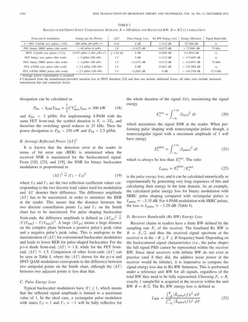
For the p-i-n diode front-end of this paper, the maximumdissipation is Pdis = 6 mW, and for 100 kbits/s, Tb =10 μs/bit; therefore, Ebit = 60 nJ/bit. Comparison can bemade with the energy per bit of 400 nJ/bit for the 2× p-i-nQAM modulator of [16] in Table I.
For MOSFET circuits, the power dissipation can be calcu-lated based on the supply voltage, gate leakage current, andswitching dissipation. For the FET front-end of this paper,the maximum bias voltage is Vmax = 2 V, the gate leakagecurrent and the gate capacitance are IGSS = 100 nA andC = 1 pF, and the maximum switching speed for 100 kbits/sis fmax = 1/(2Tb) = 50 kHz. Then the maximum power
4784 IEEE TRANSACTIONS ON MICROWAVE THEORY AND TECHNIQUES, VOL. 64, NO. 12, DECEMBER 2016
TABLE I
BACKSCATTER FRONT-ENDS’ COMPARISON. BITRATE: R = 100 kbits/s AND RECEIVER BW: B = R/2 (1 SAMPLE/BIT)
dissipation can be calculated as
Pdis < IGSSVmax + 1
2CV 2
max fmax = 300 nW (18)
and Ebit < 3 pJ/bit. For implementing 4-PAM with thesame FET front-end, the symbol duration is Ts = 2Tb, andtherefore the switching speed reduces to 25 kHz. Then thepower dissipation is Pdis < 250 nW and Ebit < 2.5 pJ/bit.
B. Average Reflected Power |�|2
It is known that the detection error at the reader interms of bit error rate (BER) is minimized when thereceived SNR is maximized for the backscattered signal.From [18], [25], and [19], the SNR for binary backscattermodulators is proportional to
|�|2 = |�1 − �0|2 (19)
where �0 and �1 are the two reflection coefficient values cor-responding to the two discrete load values used for modulationand � denotes their difference. The difference amplitude|�| has to be maximized, in order to minimize the BERat the reader. This means that the distance between thetwo discrete constellation points �0 and �1 on the Smithchart has to be maximized. For pulse shaping backscatter
front-ends, the difference amplitude is defined as |�ps|2 =|�(Vmin) − �(Vmax)|2. A large |�ps| means a large distanceon the complex plane between a positive pulse’s peak valueand a negative pulse’s peak value. This is analogous to themaximization of |�| for conventional backscatter modulatorsand leads to lower BER for pulse-shaped backscatter. For thep-i-n diode front-end, |�| ≈ 1.8, while for the FET front-end, |�| ≈ 1.5. Comparison of other front-ends |�| canbe seen in Table I, where the |�| shown for the p-i-n andSP4T QAM modulators corresponds to the difference betweentwo antipodal points on the Smith chart, although the |�|between two adjacent points is less than that.
C. Pulse Energy Loss
Typical backscatter modulators have |�| ≤ 1, which meansthat the reflected signal amplitude is limited to a maximumvalue of 1. In the ideal case, a rectangular pulse modulatorwith states �0 = 1 and �1 = −1 will be fully reflective for
the whole duration of the signal x(t), maximizing the signalenergy
E rectx =
∫ +∞
−∞|xrect|2 dt (20)
which maximizes the signal SNR at the reader. When per-forming pulse shaping with nonrectangular pulses though, anonrectangular signal with a maximum amplitude of 1 willhave energy
Epulsex =
∫ +∞
−∞|xpulse|2 dt (21)
which is always be less than E rectx . The ratio
Lpulse = Epulsex /E rect
x (22)
is the pulse energy loss, and it can be calculated numerically orexperimentally by generating very long sequences of bits andcalculating their energy in the time domain. As an example,the calculated pulse energy loss for binary modulation withSRRC pulse shaping compared with rectangular pulses isLpulse ≈ −3.35 dB. For 4-PAM modulation with SRRC pulses,the loss is Lpulse ≈ −3.29 dB (Table I).
D. Receiver Bandwidth (Rx BW) Energy Loss
Receiver chains in readers have a finite BW defined by thesampling rate Fs of the receiver. The baseband Rx BW isB = Fs/2, and thus the received signal spectrum at thereceiver is in the −B ≤ F ≤ B frequency band. Depending onthe backscattered signal characteristics (i.e., the pulse shape)the full signal PSD cannot be represented within the receiverBW. Since ideal receivers with infinite BW do not exist inpractice (and if they did, the additive noise power at thereceiver would be infinite), it is imperative to compare thesignal energy loss due to Rx BW finiteness. This is performedunder a reference unit BW for all signals, regardless of thetotal BW they need to be fully represented. Choosing Fs = R,exactly 1 sample/bit is acquired at the receiver within the unitBW B = R/2. The Rx BW energy loss is defined as
LBW =∫ B−B |Xpulse( f )|2 d F∫ ∞−∞ |Xpulse( f )|2 d F
(23)

KIMIONIS AND TENTZERIS: PULSE SHAPING: MISSING PIECE OF BACKSCATTER RADIO AND RFID 4785
and can be calculated (or approximated) numerically by com-puting X( f ), the Fourier transform of xpulse(t), for any pulseshape. As an example, the Rx BW energy loss for binary mod-ulation with rectangular pulses is LBW ≈ −1.11 dB, while forbinary modulation with SRRC pulses, it is LBW ≈ −0.41 dB.This is intuitive, due to the higher spectral efficiency of SRRCpulses compared with rectangular pulses. Other calculatedRx BW energy loss values can be seen in Table I, where inter-esting comparisons can be made between different modulationschemes and pulse shapes.
E. Energy Efficiency
An energy efficiency metric shall be defined that involvesa front-end’s energy per bit and reflected power capability, aswell as the respective pulse energy loss and Rx BW energyloss
e = |�|2Ebit
Lpulse LBW (bits/J). (24)
The formula intuitively expresses how much the energy spentfor each bit is worth in terms of useful signal SNR atthe reader. It takes into account the modulation scheme,constellation size, pulse shape, finite Rx BW, and the front-end circuit implementation. The formula can be fairly used fordirect comparisons between front-ends as in Table I, where theincreased efficiency of each front-end can be seen.
It is shown that for a constellation size of M = 4, thispaper’s front-end with binary modulation has an increasedenergy efficiency when compared with the two 4-QAM front-ends of the same data rate, with or without SRRC pulseshaping. For the FET front-end, when binary modulationand SRRC pulse shaping are used, the energy efficiencyis 2.5 dB lower compared with using the same FET withrectangular pulses. This is mainly due to the pulse energyloss, but comes at the benefit of a significantly reduced BW of75 kHz, compared with the infinite rectangular pulses BW. TheFET front-end shows an increased performance with higherorder constellations, e.g., compared with the SP4T 4-QAMfront-end, it is 7.2 dB more efficient with rectangular 4-PAM,and 4.33 dB more energy efficient with SRRC-shaped 4-PAM,while also featuring a reduced signal BW of 37.5 kHz. Fromthese results, it can be derived that the FET pulse shapingfront-end would be favorable to use for power-limited andBW-limited systems.
F. Link Budgets
The received power from a pulse shaping modulator can becalculated with [25]
PR = PTGT G R G2
tagλ4
(4π)4r2T r2
R
|�|24
(25)
where GT and G R are the gains of the reader transmit andreceive antennas, Gtag is the gain of the tag antenna, λ = c/ fc
is the wavelength, and rT and rT are the distance betweenthe transmitter and tag and the distance between the tag andreceiver, respectively. For a monostatic reader, G R = GT
and rT = rR . The received SNR from a pulse shapingmodulator is
SNR = PR K
NF N0 BLpulse LBW (26)
where N0 = −174 dBm/Hz is the noise PSD, K= Fs/R is
the number of received samples/bit (oversampling factor), Bis the receiver BW, and NF is the receiver noise figure.
For the FET modulator of this paper performing binarymodulation with SRRC shaping, a maximum communicationrange can be found for |�| = 1.5, PT = 15 dBm(SDR output power), NF = 10 dB, B = 500 kHz(K = 10 samples/bit), GT = G R = Gtag = 2.15 dBi, andfc = 913 MHz. The threshold is set to a high SNR valueof 10 dB, to achieve a minor BER value of 10−5 ([1]),which gives a maximum monostatic range of 45 m. However,utilizing bistatic architectures the tag-to-receiver distance canbe boosted to 100+ m [7], [9].
VIII. PRACTICAL MCU IMPLEMENTATION
To demonstrate the feasibility of generating arbitrary wave-forms and perform pulse shaping on low computational powerplatforms, the backscatter communication block in Fig. 12has been ported on an off-the-shelf MCU board as a proofof concept. The Silicon Labs C8051F120 MCU has beenutilized, with a typical current consumption of 2.431 mAat 3 V, with a system clock of 3.0625 MHz [26]. The F120incorporates a 12-bit digital-to-analog converter (DAC) thatis capable of generating arbitrary waveforms with a typicalcurrent consumption of 110 μA, which corresponds to a 4.5%power consumption increase for the MCU. Although the F120MCU has been used as an example, other lower consumptioncommercial MCUs can be utilized with the same principles.
The MCU has been set up to output 50-bit SRRC-shapedbitstreams at 100 kbits/s, translated to output voltage levelsthat are routed to the DAC unit. The DAC output terminaldrives the BF1118 FET transistor front-end, and the MCUeffectively replaces the V-source block in Fig. 17. A photoof the Silicon Labs development kit and the front-end can beseen in Fig. 23. It is noted that no other peripherals on theboard are utilized (e.g., serial transceiver IC, external crystaloscillator, etc.), and therefore the system can be implementedon a single board hosting only the MCU, the FET front-end,and a connector for the JTAG programming pins and powerpins, where a 3 V coin cell battery holder, or a solar cell, ora harvester’s output port can be interfaced.
The wirelessly received waveform of the MCU-modulateddata can be seen in Fig. 19(e) for comparison with theother SDR-received waveforms. The SDR-received spectrumof the FET front-end driven by the MCU can be seenin Fig. 22, where a sidelobe suppression of up to 35 dB isachieved. This can be further improved with the utilization ofa higher resolution DAC; detailed information on optimizedDAC operation and how quantization (bit resolution) affectsthe signal spectrum can be found in several publications andwhitepapers (see [27]–[29]). The DAC utilized for this paperas a proof of concept has a resolution of 12 bits, a typical

4786 IEEE TRANSACTIONS ON MICROWAVE THEORY AND TECHNIQUES, VOL. 64, NO. 12, DECEMBER 2016
Fig. 23. Pulse-shaping FET front-end interfaced to MCU board.Only the MCU and JTAG programming connector are utilized from thedevelopment kit.
Fig. 24. Pulse-shaping implementation options.
power consumption of 110 μA, and a slew rate of 0.44 V/μsfor a 40-pF load, which is more than adequate for the FETmodulator since the load (FET gate) capacitance is 1 � 40 pFand no sharp transitions from a full-OFF (0 V) to full-ON
(2 V) level are required. The transitions are always slower thanfmax = 1/(2Tbit) = 50 kHz and would require in maximum aslew rate of Vmax/(2Tb) = 2 V/20 μs = 0.1 V/μs.
Another option for generating analog signals involves thepulsewidth modulator (PWM) unit available on many MCUs.A PWM outputs pulses of variable width that can be filteredwith a low-pass network to generate analog waveforms. Theimplementation details are MCU specific, but examples canbe found in [30]–[33]. The main challenge with this approachis the design of the filter in terms of sharp cutoff (dB/octave)and in-band signal attenuation.
An even more minimal approach for pulse shaping can bethe utilization of a fully passive RLC low-pass network tofilter rectangular pulse-modulated bitstreams as they come outof a tag’s digital port and before they drive the backscattermodulator. For example, Gaussian pulse shaping could beachieved by constructing an LC low-pass Gaussian filter tosuppress the high-frequency components of rectangular pulses
that drive the front-end’s transistor [34], [35]. The main limita-tion with this approach is that the pulse shape is ‘hardcoded’ inthe circuit, and thus no arbitrary waveforms can be generated;despite that, it can be an appealing practical implementationfor non-MCU tags, such as the ones in [36] and [23], wherethe only option is to switch between two impedance states andno DACs or PWMs are available. The complexity reductionby removing the need of a DAC or PWM comes at thecost of increased signal processing at the reader, e.g., in thecase that Gaussian filters are implemented, the pulse-shapedbitstreams will suffer from ISI. Moreover, due to the factthat in general there is no linear relationship between thebias voltage Vbias(t) and the reflection coefficient �(t), thebackscattered pulses will be distorted, which translates inadditional signal processing steps at the reader (equalization),as well as undesired increase of the pulses’ BW.
The three options for implementing pulse shaping on a tagare summarized in Fig. 24. The first (DAC) is the most flexiblein terms of arbitrary signal generation, while the last (passiveLPF at a digital general purpose IO pin of an MCU) gives theless flexibility, but lowest complexity and power consumption.
IX. CONCLUSION
An extensive presentation was given of the concepts behindbackscatter pulse shaping, along with the signal processing andthe front-end implementations to achieve it. The principle ofcontinuously varying the tag reflection coefficient and how thistranslates to pulse-shaped backscatter signals was analyzedand demonstrated with very low complexity front-ends thatutilize a single nonlinear component, e.g., a p-i-n diode or aFET transistor. Despite the front-ends’ low complexity andminimized energy footprint, they can effectively break thelimitations of rectangular waveforms and high BW occu-pancy found in conventional RFID tags. SRRC pulses werecreated and backscattered as a proof of concept, but otherarbitrary pulses can be generated as well. Tags can essentiallybecome miniature SDRs to implement diverse communicationschemes, spectral characteristics, or modulation formats. Thispaper has offered a missing piece to complete backscatter radioas a communication scheme for low-complexity low-energysensor tags and computational RFID.
REFERENCES
[1] J. G. Proakis, Digital Communications, 4th ed. New York, NY, USA:McGraw-Hill, 2001.
[2] S. J. Maeng and B. G. Lee, “A design of linear-phased IIR Nyquistfilters,” IEEE J. Sel. Areas Commun., vol. 13, no. 1, pp. 167–175,Jan. 1995.
[3] D. M. Dobkin, The RF in RFID: Passive UHF RFID in Practice.Newton, MA, USA: Elsevier, 2008.
[4] A. P. Sample, D. J. Yeager, P. S. Powledge, and J. R. Smith,“Design of a passively-powered, programmable sensing platform forUHF RFID systems,” in Proc. IEEE Int. Conf. RFID, Mar. 2007,pp. 149–156.
[5] EPC Radio-Frequency Identity Protocols, Class-1 Generation-2 UHFRFID Protocol for Communications at 860MHz–960MHz, Version 1.2.0,EPC Global, 2008.
[6] J. Kimionis, A. Bletsas, and J. N. Sahalos, “Design and imple-mentation of RFID systems with software defined radio,” inProc. 6th Eur. Conf. Antennas Propag. (EUCAP), Mar. 2012,pp. 3464–3468.

KIMIONIS AND TENTZERIS: PULSE SHAPING: MISSING PIECE OF BACKSCATTER RADIO AND RFID 4787
[7] G. Vougioukas, S.-N. Daskalakis, and A. Bletsas, “Could battery-less scatter radio tags achieve 270-meter range?” in Proc. IEEEWireless Power Transf. Conf., Aveiro, Portugal, May 2016,pp. 1–3.
[8] J. Kimionis, A. Bletsas, and J. N. Sahalos, “Bistatic backscat-ter radio for tag read-range extension,” in Proc. IEEE Int.Conf. RFID-Technol. Appl. (RFID-TA), Nice, France, Nov. 2012,pp. 356–361.
[9] J. Kimionis, A. Bletsas, and J. N. Sahalos, “Increased range bistaticscatter radio,” IEEE Trans. Commun., vol. 62, no. 3, pp. 1091–1104,Mar. 2014.
[10] V. Liu, A. Parks, V. Talla, S. Gollakota, D. Wetherall, and J. R.Smith, “Ambient backscatter: Wireless communication out of thin air,”in Proc. ACM SIGCOMM Conf. (SIGCOMM), Hong Kong, 2013,pp. 39–50.
[11] S. J. Thomas, E. Wheeler, J. Teizer, and M. S. Reynolds, “Quadra-ture amplitude modulated backscatter in passive and semipassive UHFRFID systems,” IEEE Trans. Microw. Theory Techn., vol. 60, no. 4,pp. 1175–1182, Apr. 2012.
[12] R. Correia and N. B. Carvalho, “Design of high order modulationbackscatter wireless sensor for passive IoT solutions,” in Proc. IEEEWireless Power Transf. Conf., Aveiro, Portugal, May 2016, pp. 1–3.
[13] Y. Ma, X. Hui, and E. C. Kan, “Harmonic-WISP: A passive broadbandharmonic RFID platform,” in IEEE MTT-S Int. Microw. Symp. Dig.,San Francisco, CA, USA, May 2016, pp. 1–4.
[14] J. Kimionis and M. M. Tentzeris, “Software-defined reader for multi-modal RFID sensing,” in IEEE MTT-S Int. Microw. Symp. Dig.,San Francisco, CA, USA, May 2016, pp. 1–4.
[15] Y. Taur and T. H. Ning, Fundamentals of Modern VLSI Devices, 2nd ed.Cambridge, U.K.: Cambridge Univ., 2013.
[16] M. Winkler, T. Faseth, H. Arthaber, and G. Magerl, “An UHF RFIDtag emulator for precise emulation of the physical layer,” in Proc. Eur.Wireless Technol. Conf. (EuWIT), Paris, France, Sep. 2010, pp. 273–276.
[17] V. Viikari, J. Chisum, and H. Seppa, “Wireless passive photo detectorfor insect tracking,” Microw. Opt. Technol. Lett., vol. 52, no. 10,pp. 2312–2315, Jul. 2010.
[18] F. Fuschini, C. Piersanti, F. Paolazzi, and G. Falciasecca, “Analyticalapproach to the backscattering from UHF RFID transponder,”IEEE Antennas Wireless Propag. Lett., vol. 7, pp. 33–35,Feb. 2008.
[19] A. Bletsas, A. G. Dimitriou, and J. N. Sahalos, “Improving backscatterradio tag efficiency,” IEEE Trans. Microw. Theory Techn., vol. 58, no. 6,pp. 1502–1509, Jun. 2010.
[20] N. S. Alagha and P. Kabal, “Generalized raised-cosine filters,” IEEETrans. Commun., vol. 47, no. 7, pp. 989–997, Jul. 1999.
[21] J. Kimionis, A. Georgiadis, A. Collado, and M. M. Tentzeris, “Enhance-ment of RF tag backscatter efficiency with low-power reflectionamplifiers,” IEEE Trans. Microw. Theory Techn., vol. 62, no. 12,pp. 3562–3571, Dec. 2014.
[22] J. Kimionis and M. M. Tentzeris, “RF tag front-end design for uncom-promised communication and harvesting,” in Proc. IEEE RFID Technol.Appl. Conf. (RFID-TA), Tampere, Finland, Sep. 2014, pp. 109–114.
[23] E. Kampianakis, J. Kimionis, K. Tountas, C. Konstantopoulos,E. Koutroulis, and A. Bletsas, “Wireless environmental sensornetworking with analog scatter radio and timer principles,” IEEESensors J., vol. 14, no. 10, pp. 3365–3376, Oct. 2014.
[24] ADG904 4:1 Mux/SP4T, Datasheet, Analog Devices, Norwood, MA,USA, 2013.
[25] J. D. Griffin and G. D. Durgin, “Complete link budgets for backscatter-radio and RFID systems,” IEEE Antennas Propag. Mag., vol. 51, no. 2,pp. 11–25, Feb. 2009.
[26] C8051F12x and C8051F13x Mixed-Signal ISP Flash MCU Family,Datasheet, Silicon Labs, Austin, TX, USA, 2003.
[27] “Understanding data converters,” Texas Instrum., Dallas, TX, USA,Tech. Rep. SLAA013, 1995.
[28] P. Xiao, C. Toal, D. Burns, V. Fusco, and C. Cowan, “Transmitand receive filter design for OFDM based WLAN systems,” in Proc.Int. Conf. Wireless Commun. Signal Process., vol. 1. Oct. 2010,pp. 1–4.
[29] V. Agarwal, P. Kim, D.-G. Oh, and D.-S. Ahn, “Hardware effi-cient root-raised-cosine pulse shaping filter for DVB-S2 receivers,” inAdvances in Computing and Communications, A. Abraham, J. L. Mauri,J. F. Buford, J. Suzuki, and S. M. Thampi, Eds. Berlin, Germany:Springer, 2011, pp. 595–603.
[30] M. Mitchell, “Using PWM timer_B as a DAC,” Texas Instrum., Dallas,TX, USA, Appl. Rep. SLAA116, Dec. 2000.
[31] “16-bit PWM using an on-chip timer,” Silicon Labs, Austin, TX, USA,Appl. Note AN110, Dec. 2003.
[32] D. M. Alter, “Using PWM output as a digital-to-analog converter ona TMS320F280x digital signal controller,” Texas Instrum., Dallas, TX,USA, App. Rep. SPRAA88A, Sep. 2008.
[33] R. Metivier, “Method for converting a PWM output to an analog outputwhen using Hall-effect sensor ICs,” Allegro Microsyst., LLC, Worcester,MA, USA, Appl. Note 296094-AN, 2013.
[34] L. Besser and R. Gilmore, Practical RF Circuit Design for ModernWireless Systems, vol. 2. Norwood, MA, USA: Artech House, 2003.
[35] J.-S. G. Hong and M. J. Lancaster, Microstrip Filters for RF/MicrowaveApplications. Hoboken, NJ, USA: Wiley, 2004.
[36] A. Strobel, C. Carlowitz, R. Wolf, F. Ellinger, and M. Vossiek,“A millimeter-wave low-power active backscatter tag for FMCWradar systems,” IEEE Trans. Microw. Theory Techn., vol. 61, no. 5,pp. 1964–1972, May 2013.
John Kimionis (S’10) received the Diploma degreeand M.Sc. degree in electronic and computer engi-neering from the Technical University of Crete, Cha-nia, Greece, in 2011 and 2013, respectively, wherehe was with the Telecom Lab.
He is currently a Ph.D. candidate with the Schoolof Electrical and Computer Engineering, GeorgiaInstitute of Technology, Atlanta, GA, USA, and aResearch Assistant with the ATHENA Group. Hisresearch interests are in the areas of spectral-efficientand energy-efficient backscatter radio and RFID,
software-defined radio for sensor networks, RF front-end design for wirelesssensors, and additive manufacturing techniques.
Mr. Kimionis was the recipient of fellowship awards for his undergraduateand graduate studies and he is a Texas Instruments Scholar for his mentoringservice for the Opportunity Research Scholars (ORS) program at the GeorgiaInsitute of Technology. He was the recipient of IEEE student travel grants,the First Best Student Paper Award of the IEEE International Conferenceon RFID-Technologies and Applications (RFID-TA) 2014, Tampere, Finland,as well as the Second Best Student Paper Award of the IEEE InternationalConference on RFID-Technologies and Applications (RFID-TA) 2011, Sitges,Barcelona, Spain. He has been a member of the IEEE Microwave Theory andTechniques Society, the IEEE Communications Society, and a board memberof the IEEE MTT-24 RFID Technologies Committee.
4788 IEEE TRANSACTIONS ON MICROWAVE THEORY AND TECHNIQUES, VOL. 64, NO. 12, DECEMBER 2016
Manos M. Tentzeris (S’89–M’92–SM’03–F’10)received the Diploma degree (magna cum laude)in electrical and computer engineering from theNational Technical University of Athens, Athens,Greece, and the M.S. and Ph.D. degrees in electricalengineering and computer science from the Univer-sity of Michigan, Ann Arbor, MI, USA.
He has served as the Head of the Georgia TechElectrical and Computer Engineering Electromag-netics Technical Interest Group at the GeorgiaInstitute of Technology, Atlanta, GA, USA, as an
Associate Director for RFID/Sensors research at the Georgia ElectronicDesign Center, Atlanta, and as an Associate Director for RF Research atthe GT NSF-Packaging Research Center, where he was also the RF AllianceLeader. He was a Visiting Professor with the Technical University of Munich,Munich, Germany, in 2002, a Visiting Professor with GTRI-Ireland, Athlone,Ireland, in 2009, and a Visiting Professor with LAAS-CNRS, Toulouse,France, in 2010. He is currently a Ken Byers Professor of flexible electronicswith the School of Electrical and Computer Engineering, Georgia Institute ofTechnology. He is the Head of the Athena research group (20 researchers).He has authored more than 620 papers in refereed journals and conferenceproceedings, five books, and 25 book chapters. He has helped to develop acad-emic programs in 3-D/inkjet-printed RF electronics and modules, flexible elec-tronics, origami and morphing electromagnetics, highly integrated/multilayerpackaging for RF and wireless applications using ceramic and organicflexible materials, paper-based RFID’s and sensors, wireless sensors andbiosensors, wearable electronics, “Green” electronics, energy harvesting andwireless power transfer, nanotechnology applications in RF, MicrowaveMEM’s, and SOP-integrated (UWB, multiband, mmW, and conformal)antennas.
Dr. Tentzeris was a recipient/corecipient of the 2015 IET Microwaves,Antennas, and Propagation Premium Award, the 2014 Georgia Tech ECEDistinguished Faculty Achievement Award, the 2014 IEEE RFID-TA BestStudent Paper Award, the 2013 IET Microwaves, Antennas, and Propagation
Premium Award, the 2012 FiDiPro Award in Finland, the iCMG ArchitectureAward of Excellence, the 2010 IEEE Antennas and Propagation SocietyPiergiorgio L. E. Uslenghi Letters Prize Paper Award, the 2011 InternationalWorkshop on Structural Health Monitoring Best Student Paper Award, the2010 Georgia Tech Senior Faculty Outstanding Undergraduate ResearchMentor Award, the 2009 IEEE TRANSACTIONS ON COMPONENTS AND
PACKAGING TECHNOLOGIES Best Paper Award, the 2009 E.T.S.WaltonAward from the Irish Science Foundation, the 2007 IEEE APS SymposiumBest Student Paper Award, the 2007 IEEE IMS Third Best Student PaperAward, the 2007 ISAP 2007 Poster Presentation Award, the 2006 IEEE MTTOutstanding Young Engineer Award, the 2006 Asian-Pacific Microwave Con-ference Award, the 2004 IEEE TRANSACTIONS ON ADVANCED PACKAGING
Commendable Paper Award, the 2003 NASA Godfrey "Art" Anzic Collabo-rative Distinguished Publication Award, the 2003 IBC International Educatorof the Year Award, the 2003 IEEE CPMT Outstanding Young EngineerAward, the 2002 International Conference on Microwave and Millimeter-WaveTechnology Best Paper Award (Beijing, China), the 2002 Georgia Tech-ECEOutstanding Junior Faculty Award, the 2001 ACES Conference Best PaperAward, the 2000 NSF CAREER Award, and the 1997 Best Paper Awardof the International hybrid Microelectronics and Packaging Society. He wasthe TPC Chair for the IEEE IMS 2008 Symposium and the Chair of the2005 IEEE CEM-TD Workshop and is the Vice-Chair of the RF TechnicalCommittee (TC16) of the IEEE CPMT Society. He served as one of the IEEEMTT-S Distinguished Microwave Lecturers from 2010 to 2012 and is one ofthe IEEE CRFID Distinguished Lecturers. He is the Founder and has servedas the Chair of the RFID Technical Committee (TC24) of the IEEE MTTSociety and is the Secretary/Treasurer of the IEEE C-RFID. He has served asthe Associate Editor of the IEEE TRANSACTIONS ON MICROWAVE THEORYAND TECHNIQUES, the IEEE TRANSACTIONS ON ADVANCED PACKAGING,and the International Journal on Antennas and Propagation. He has givenmore than 100 invited talks to various universities and companies all over theworld. He is a member of the URSI-Commission D, a member of the MTT-15Committee, an Associate Member of EuMA, a fellow of the ElectromagneticAcademy, and a member of the Technical Chamber of Greece.