4.5 Biasing in BJT Amplifier Circuits - KU ITTCjstiles/412/handouts/4.5 Biasing in MOS Amp... ·...
41
4/25/2011 section 4_5 Biasing in MOS Amplifier Circuits 1/2 Jim Stiles The Univ. of Kansas Dept. of EECS 4.5 Biasing in BJT Amplifier Circuits Reading Assignment: 280-286 Now let’s examine how we DC bias MOSFETs amplifiers! If we don’t bias properly, distortion can result! EXAMPLE: MOSFET AMPLIFIER DISTORTION There is a classic bias circuit for MOSFET amplifiers; let’s see what it is! HO: MOSFET BIASING USING A SINGLE POWER SUPPLY Let’s do an example DC bias design. EXAMPLE: BIASING OF DISCRETE MOSFET AMPLIFIERS We can also use a DC current source to bias the Amplifier. Q: Yes, but just how do we construct a current source? A: HO:THE MOSFET CURRENT MIRROR HO: CURRENT STEERING CIRCUITS
Transcript of 4.5 Biasing in BJT Amplifier Circuits - KU ITTCjstiles/412/handouts/4.5 Biasing in MOS Amp... ·...

4/25/2011 section 4_5 Biasing in MOS Amplifier Circuits 1/2
Jim Stiles The Univ. of Kansas Dept. of EECS
4.5 Biasing in BJT Amplifier Circuits
Reading Assignment: 280-286
Now let’s examine how we DC bias MOSFETs amplifiers! If we don’t bias properly, distortion can result! EXAMPLE: MOSFET AMPLIFIER DISTORTION There is a classic bias circuit for MOSFET amplifiers; let’s see what it is! HO: MOSFET BIASING USING A SINGLE POWER SUPPLY Let’s do an example DC bias design. EXAMPLE: BIASING OF DISCRETE MOSFET AMPLIFIERS We can also use a DC current source to bias the Amplifier. Q: Yes, but just how do we construct a current source? A: HO:THE MOSFET CURRENT MIRROR HO: CURRENT STEERING CIRCUITS

4/25/2011 section 4_5 Biasing in MOS Amplifier Circuits 2/2
Jim Stiles The Univ. of Kansas Dept. of EECS
HO: MOSFET BIASING USING CURRENT MIRRORS EXAMPLE: MOSFET BIASING USING CURRENT MIRRORS

4/25/2011 Example MOSFET Amplifier Distortion 1/9
Example: MOSFET Amplifier Distortion
Recall this circuit from a previous handout: We found that the small-signal voltage gain is:
( ) 5.0( )
ovo
i
v tAv t
= = −
15.0 V
5DR K=
( ) ( )D D di t I i t= +
.4 0V
( )iv t
( ) ( )O D ov t V v t= +
+ -
20.25 mA/V
2.0 Vt
K
V
=
=

4/25/2011 Example MOSFET Amplifier Distortion 2/9
Say the input voltage to this amplifier is:
( ) cosi iv t V ωt=
Q: What is the largest value that Vi can take without producing a distorted output?
A: Well, we know that the small-signal output is:
( ) ( )5.0 cos
o vo i
i
v t A v tV ωt
=
= −
BUT, this is not the output voltage! The total output voltage is the sum of the small-signal output voltage and the DC output voltage! Note for this example, the DC output voltage is the DC drain voltage, and we recall we determined in an earlier handout that its value is:
10 VO DV V= =
Thus, the total output voltage is :
( ) ( )10.0 5.0 cos
O D o
i
v t V v tV ωt
= +
= −

4/25/2011 Example MOSFET Amplifier Distortion 3/9
It is very important that you realize there is a limit on both how high and how low the total output voltage ( )Ov t can go!
That’s right! If the total output voltage
( )Ov t tries to exceed these limits—even for a moment—theMOSFET will leave saturation mode.
And leaving saturation mode results in signal distortion!

4/25/2011 Example MOSFET Amplifier Distortion 4/9
Let’s break the problem down into two separate problems:
1) If total output voltage ( )Ov t becomes too small, the MOSFET will enter the triode mode. 2) If total output voltage ( )Ov t becomes too large, the MOSFET will enter cutoff.
We’ll first consider problem 1. For a MOSFET to remain in saturation, ( )DSv t must remain greater than the excess gate voltage ( )GS tV V− for all time t. ( )
DS GS tv t V V> − Since the source terminal of the MOSFET in this circuit is connected to ground, we know that 0 VSV = . Therefore:
( ) ( ) ( )DS D Ov t v t v t= = and GS GV V= And so the MOSFET will remain in saturation only if the total output voltage remains larger than GS t G tV V V V− = − !
( )O G tv t V V> −

4/25/2011 Example MOSFET Amplifier Distortion 5/9
Thus, we conclude for this amplifier that the output “floor” is: G tL V V− = − And since 4.0GV V= and 2.0tV V= , we find:
4 2 2.0G tL V V V− = − = − =
Thus, to remain in saturation, the total output voltage must remain larger than the “floor” voltage L− for all time t :
( ) 2.0Ov t L V−> =
Since this total voltage is:
10.0 5.( ) 0 cosO iV ωtv t −= we can determine the maximum value of small-signal input magnitude iV :
10.0 5.0 cos 2.0
8.0 5.0 cos
cos 1.6
i
i
i
V ωt
V ωt
V ωt
− >
⇒ >
⇒ <
4/25/2011 Example MOSFET Amplifier Distortion 6/9
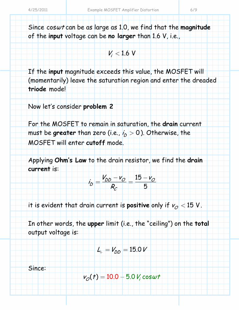
Since cosωt can be as large as 1.0, we find that the magnitude of the input voltage can be no larger than 1.6 V, i.e.,
1.6 ViV <
If the input magnitude exceeds this value, the MOSFET will (momentarily) leave the saturation region and enter the dreaded triode mode! Now let’s consider problem 2 For the MOSFET to remain in saturation, the drain current must be greater than zero (i.e., 0Di > ). Otherwise, the MOSFET will enter cutoff mode. Applying Ohm’s Law to the drain resistor, we find the drain current is:
155
DD O OD
C
V v viR− −
= =
it is evident that drain current is positive only if 15 VOv < . In other words, the upper limit (i.e., the “ceiling”) on the total output voltage is:
15.0DDL V V+ = = Since:
10.0 5.( ) 0 cosO iV ωtv t −=

4/25/2011 Example MOSFET Amplifier Distortion 7/9
we can conclude that in order for the MOSFET to remain in saturation mode:
10 5.0 cos 15.0iV ωt− > Therefore, we find:
5.0cos 1.05.0sV ωt −
> = −
Since cos 1ωt ≥− , the above equation means that the input signal magnitude Vi can be no larger than:
1.0 ViV <
If the input magnitude exceeds 1.0 V, the MOSFET will (momentarily) leave the saturation and enter the cutoff region! In summary:
1) If 1.6 ViV > , the MOSFET will at times enter triode, and distortion will occur! 2) If 1.0 ViV > , the MOSFET will at times enter cutoff, and even more distortion will occur!

4/25/2011 Example MOSFET Amplifier Distortion 8/9
To demonstrate this, let’s consider three examples: 1. 1.0 ViV <
The output signal in this case remains between 15.0DDV = and
2.0G tV V− = V for all time t. Therefore, the output signal is not distorted.
2. 1.6 V 1.0 ViV> >
The output signal in this case remains greater than 2G tL V V− = =− for all time t. However, the small-signal output is now large enough so that the total output voltage at times tries to exceed
15DDL V+ = = . For these times, the MOSFET will enter cutoff, and the output signal will be distorted.
15DDL V+ = =
10OV =
t
( )Ov t
2G tL V V− = =−

4/25/2011 Example MOSFET Amplifier Distortion 9/9
3. 1.6iV V> In this case, the small-signal input signal is sufficiently large so that the total output will attempt to exceed both limits (i.e.,
15.0VDDV = and 2.0VG tV V− = ). Therefore, there are periods of time when the MOSFE will be in cutoff, and periods when the MOSFET will be in saturation.
15DDL V+ = =
10OV =
t
( )Ov t
2G tL V V− = =−
15DDL V+ = =
10OV =
t
( )Ov t
2G tL V V− = =−

4/25/2011 MOSFET Biasing using a Single Power Supply 1/9
MOSFET Biasing using a Single Power Supply
The general form of a single-supply MOSFET amplifier biasing circuit is: Just like BJT biasing, we typically attempt to satisfy three main bias design goals: 1) Maximize Gain Typically, the small-signal voltage gain of a MOSFET amplifier will be proportional to transconductance mg :
1R
2R
DR
SR
DDV DDV
DI
+
DSV -
+ GSV
-

4/25/2011 MOSFET Biasing using a Single Power Supply 2/9
vo mA g∝
Thus, to maximize the amplifier voltage gain, we must maximize the MOSFET transconductance. Q: What does this have to do with D.C. biasing? A: Recall that the transconductance depends on the DC excess gate voltage:
( )2m GS tg K V V= −
Another way to consider transconductance is to express it in terms of DC drain current DI . Recall this DC current is related to the DC excess gate voltage (in satureation!) as:
( ) ( )2 DD GS t GS t
II K V V V VK
= − ⇒ − =
And so transconductance can be alternatively expressed as:
( )2 2 2Dm GS t D
Ig K V V K K IK
= − = =
Therefore, the amplifier voltage gain is typically proportional to the square-root of the DC drain current:
vo DA I∝

4/25/2011 MOSFET Biasing using a Single Power Supply 3/9
To maximize voA , maximize DI 2) Maximize Voltage Swing Recall that if the DC drain voltage DV is biased too close to DDV , then even a small small-signal drain voltage ( )dv t can result in a total drain voltage that is too large, i.e.:
( ) ( ) D D DDdv t V v t V= + ≥
In other words, the MOSFET enters cutoff, and the result is a distorted signal! To avoid this (to allow ( )dv t to be as large as possible without MOSFET entering cutoff), we need to bias our MOSFET such that the DC drain voltage DV is as small as possible. Note that the drain voltage is:
D DD D DV V R I= −
Therefore DV is minimized by designing the bias circuit such that the DC drain current DI is as large as possible.

4/25/2011 MOSFET Biasing using a Single Power Supply 4/9
However, we must also consider the signal distortion that occurs when the MOSFET enters triod. This of course is avoided if the total voltage drain-to-source remains greater than the excess gate voltage, i.e.:
( )( ) ( ) GS tDS DS ds V Vv t V v t −= + >
Thus, to avoid the MOSFET triode mode—and the resulting signal distortion—we need to bias our MOSFET such that the DC voltage DSV is as large as possible.
To minimize signal distortion, maximize DSV
3) Minimize Sensitivity to changes in , tK V We find that MOSFETs are sensitive to temperature—specifically, the value of K is a function of temperature. Likewise, the values of K and threshold voltage tV are not particularly constant with regard to the manufacturing process. Both of these facts lead to the requirement that our bias design be insensitive to the values of K and tV . Specifically, we want to design the bias network such that the DC bias current does not change values when K and/or tV does.

4/25/2011 MOSFET Biasing using a Single Power Supply 5/9
Mathematically, we can express this requirement as minimizing the value:
Dd IdK
and D
t
d IdV
Similar to the BJT, we find that these derivatives are minimized by maximizing the value of source resistor SR .
To minimize Dd I dK , maximize SR
So, let’s recap what we have learned about designing our bias network:
1. Make DI as large as possible.
2. Make DSV as large as possible.
3. Make SR as large as possible.
Again analogous to BJT biasing, we find that these three goals are conflicting, as they are constrained by the KVL equation of the bias circuit:

4/25/2011 MOSFET Biasing using a Single Power Supply 6/9
0DD D D DS D SV I R V I R− − − =
or
D D DS D S DDI R V I R V+ + =
Maximize Avo by maximizing this term.
Minimize distortion by maximizing this term.
Minimize sensitivity by maximizing this term.
But the total of the three terms must equal this!
1R
2R
DR
SR
DDV DDV
DI
+
DSV -
+ GSV
-

4/25/2011 MOSFET Biasing using a Single Power Supply 7/9
Resolving this conflict is a subject choice of the amplifier designer. However, here is a “rule-of-thumb” procedure. However, verify that these results satisfy your design requirements (or the requirements assigned to you by your boss and/or professor!). 1. Given the desired value of ID, make source voltage
4S DDV V= , i.e. set the source resistor SR to:
4DDs
SD D
VVRI I
= = (1)
This value reduces the sensitivity Dd I dK ! 2. Now determine the required value of GSV . Since
2( )tGSDI K V V= − , we find that GSV should be:
DtGS
IV VK
= +
3. Set the required value of gate voltage GV . Note that:
SG GSV V V= +
Thus, we can add the results of the previous two steps to find the required value of the gate voltage GV .

4/25/2011 MOSFET Biasing using a Single Power Supply 8/9
To set the gate voltage to this value, we must select the proper values of resistors 1 2 and R R . Since the gate current is zero ( 0Gi = ), we find from voltage division that:
2
11 22
1DD
G DDVRV V RR RR
⎛ ⎞= =⎜ ⎟+ ⎛ ⎞⎝ ⎠ +⎜ ⎟
⎝ ⎠
(2)
Note this equation determines the ratio of resistors 1 2 and R R , but not the resistors themselves. We need a second equation to explicitly determine the resistors values—the sum of the two resistances, for example. We find that making the resistances 1 2 and R R as large as possible is very desirable! This will typically maximize the amplifier input resistance, as well as result in minimum power dissipation. As a result, we make the resistors as large a practicable. For example:
1 2 250 KR R+ = (3)
4. Set the required value of DC drain voltage DV . Recall that:
a) we require D DDV V L+= to avoid cutoff mode.

4/25/2011 MOSFET Biasing using a Single Power Supply 9/9
b) and, we require that D G tV V V L−− = to avoid triode mode.
Solution: set the drain voltage DV to a value half-way between
DDV and tGV V− ! In other words, set the DC drain voltage to be:
( )2
tGDDD
V V VV
+ −=
To achieve this, we must select the drain resistor DR so that:
( )2
DD G tDD DD
D D
V V VV VRI I
− −−= = (4)
Thus, use equations (1), (2), (3), and (4) to determine the standard DC bias design (i.e., 1 2, , , and S DR R R R ) for MOSFET amplifiers.
If I were you, I’d make sure I understood this material well enough that I could also bias a non-standard MOSFET amplifier problem. It’s not enough to simply know how, you must also know why!
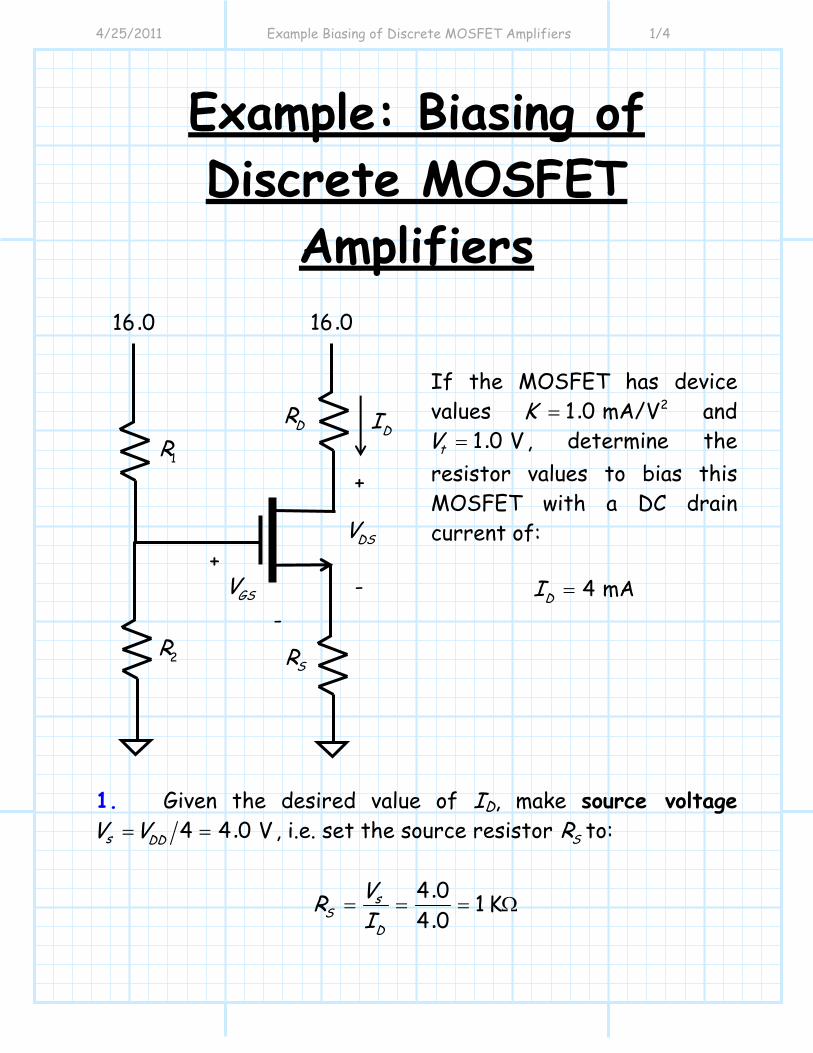
4/25/2011 Example Biasing of Discrete MOSFET Amplifiers 1/4
Example: Biasing of Discrete MOSFET
Amplifiers
If the MOSFET has device values 21 0 mA/V.K = and
1 0 V.tV = , determine the resistor values to bias this MOSFET with a DC drain current of:
4 mADI =
1. Given the desired value of ID, make source voltage
4 4 0 V.s DDV V= = , i.e. set the source resistor SR to:
4 0 1 K4 0..
sS
D
VRI
= = = Ω
1R
2R
DR
SR
16 0. 16 0.
DI
+
DSV -
+ GSV
-

4/25/2011 Example Biasing of Discrete MOSFET Amplifiers 2/4
2. Now determine the required value of GSV . Since 2( )tGSDI K V V= − , we find that GSV should be:
4 0 1 01 0
3 0 V
. ..
.
DtGS
IV VK
= +
= +
=
3. Set the required value of gate voltage GV .
3 0 4 07 0 V. ..
SG GSV V V= +
= +
=
Since the gate current is zero ( 0Gi = ), we find from voltage division that:
1
21
DDG
VV RR
=⎛ ⎞ +⎜ ⎟⎝ ⎠
Therefore:
1
21
16 0 17 097
..
DD
G
VRR V
= −
= −
=

4/25/2011 Example Biasing of Discrete MOSFET Amplifiers 3/4
We need a second equation to explicitly determine the resistors values—the sum of the two resistances, for example. We make the resistors as large a practicable. For example:
1 2 240 KR R+ = Therefore:
2 2
2
9 2407
16 2407
R R
R
+ =
=
and thus:
1 2135 K and 105 KR R= Ω = Ω
4. Set the required value of DC drain voltage DV . Set the drain voltage DV to a value half-way between DDV and
tGV V− ! In other words, set the DC drain voltage to be:
( )
( )2
16 7 0 1 02
11 0 V
. .
.
tGDDD
V V VV
+ −=
+ −=
=
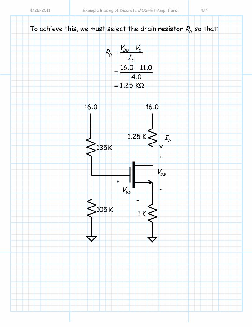
4/25/2011 Example Biasing of Discrete MOSFET Amplifiers 4/4
To achieve this, we must select the drain resistor DR so that:
16 0 11 04 0
1 25 K
. ..
.
DD DD
D
V VRI−
=
−=
= Ω
135K
105 K
1 25 K.
1 K
16 0. 16 0.
DI
+
DSV -
+ GSV
-
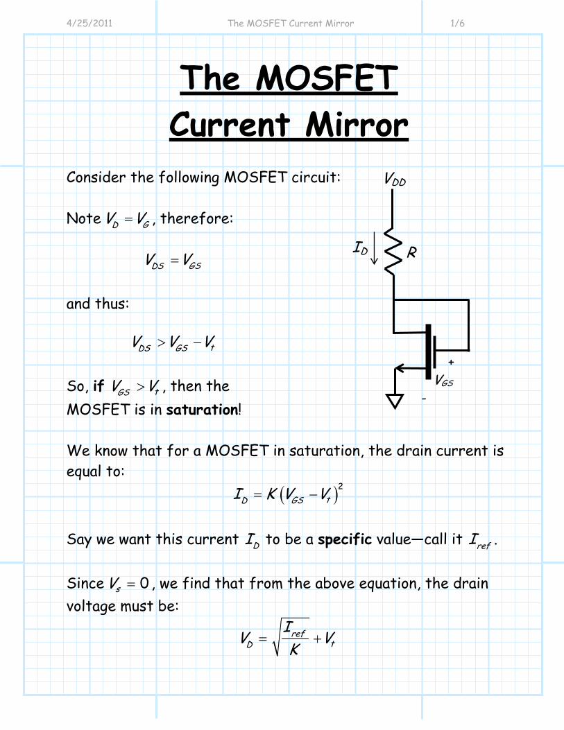
4/25/2011 The MOSFET Current Mirror 1/6
The MOSFET Current Mirror
Consider the following MOSFET circuit: Note GDV V= , therefore:
GSDSV V=
and thus:
tGSDSV V V> −
So, if tGSV V> , then the MOSFET is in saturation! We know that for a MOSFET in saturation, the drain current is equal to:
( )2tGSDI K V V= −
Say we want this current DI to be a specific value—call it refI . Since 0sV = , we find that from the above equation, the drain voltage must be:
reftD
IV VK
= +
VDD
R ID
+ VGS -

4/25/2011 The MOSFET Current Mirror 2/6
Likewise, from KVL we find that:
DD Dref
V VIR−
=
And thus the resistor value to achieve the desired drain current
refI is: DD D
ref
V VRI−
=
where: ref
tDI
V VK
= +
Q: Why are we doing this?
A: Say we now add another component to the circuit, with a second MOSFET that is identical to the first :
VDD
RL IL
+ VGS2 -
VDD
R Iref
+ VGS1 -

4/25/2011 The MOSFET Current Mirror 3/6
Q: So what is current IL ? A: Note that the gate voltage of each MOSFET is the same (i.e., 1 2GS GSV V= ), and if the MOSFETS are the same (i.e.,
1 2 1 2, t tK K V V= = ), and if the second MOSFET is likewise in saturation, its drain current LI is:
( )( )
22 2 2
21 1 1
L GS t
GS t ref
I K V V
K V V I
= −
= − =
Therefore, the drain current of the second MOSFET is equal to the current of the first!
LrefI I=
Q: Wait a minute! You mean to say that the current through the resistor RL is independent of the value of resistor RL ? A: Absolutely! As long as the second MOSFET is in saturation, the current through RL is equal to Iref—period. The current through RL is independent on the value of RL (provided that the MOSFET remains in saturation). Think about what this means—this device is a current source !
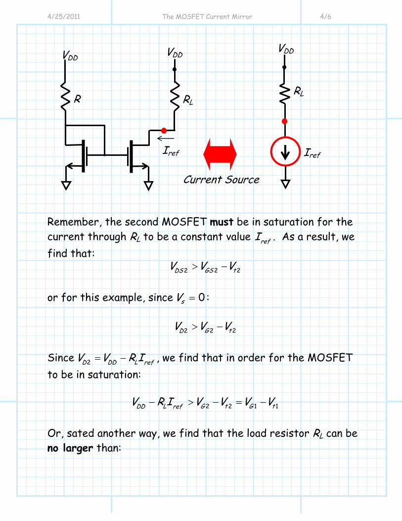
4/25/2011 The MOSFET Current Mirror 4/6
Remember, the second MOSFET must be in saturation for the current through RL to be a constant value refI . As a result, we find that:
2 22 GS tDSV V V> −
or for this example, since 0sV = :
2 22 G tDV V V> −
Since 2 LD DD refV V R I= − , we find that in order for the MOSFET to be in saturation:
2 2 1 1L G t G tDD refV R I V V V V− > − = −
Or, sated another way, we find that the load resistor RL can be no larger than:
Current Source
RL
VDD
R
Iref
VDD
Iref
RL
VDD

4/25/2011 The MOSFET Current Mirror 5/6
1 1G tDD
Lref
V V VRI− +
<
Where we know that:
1G DD refV V R I= −
and thus we can alternatively write the above equation as:
1tL
ref
VR RI
< +
If the load resistor becomes larger than 1t refR V I+ , the voltage 2DSV will drop below the excess gate voltage 2 2GS tV V− , and thus the second MOSFET will enter the triode region. As a result, the drain current will not equal refI —the current source will stop working!
Although the circuit presented here is sometimes referred to as a current sink, understand that the circuit is clearly a way of designing a current source.

4/25/2011 The MOSFET Current Mirror 6/6
We can also use PMOS devices to construct a current mirror!
VSS
RL IL
+ VGS2 -
VSS
R Iref
+ VGS1 -
This better be in saturation!
L refI I= , regardless of the value of RL!!!

4/27/2011 Current Steering Circuits 1/3
Current Steering Circuits A current mirror may consist of many MOSFET current sources! This circuit is particularly useful in integrated circuit design, where one resistor R is used to make multiple current sources. Q: What if we want to make the sources have different current values? Do we need to make additional current mirrors? A: NO!!
Recall that the current mirror simply ensures that the gate to source voltages of each transistor is equal to the gate to source voltage of the reference:
IL1 =Iref
VDD
R Iref
VDD VDD VDD
Qref Q1 Q2 Q3
RL1 RL2 RL3 IL2=Iref
IL3=Iref

4/27/2011 Current Steering Circuits 2/3
1 2 3ref
GS GS GS GSV V V V= = = =
Therefore, if each transistor is identical (i.e., 1refK K= = , and
1 2ref
t t tV V V= = = ) then:
( )( )
2
2
ref reftGSref ref
n tnGSn Dn
I K V V
K V V I
= −
= − =
In other words, if each transistor nQ is identical to refQ , then each current DnI will equal reference current refI . But, consider what happens if the MOSFETS are not identical. Specifically, consider the case where n refK K≠ (but ref
tn tV V= ). Remember, we know that ref
GSn GSV V= still, even when n refK K≠ . Thus, the drain current DnI will now be:
( )
( )
2
2
n tnGSnDn
ref refn tGS
refn
ref
nref
ref
I K V V
K V V
IKK
K IK
= −
= −
⎛ ⎞= ⎜ ⎟⎜ ⎟
⎝ ⎠⎛ ⎞
= ⎜ ⎟⎜ ⎟⎝ ⎠
The drain current is a scaled value of refI !

4/27/2011 Current Steering Circuits 3/3
For example, if 1K is twice that of refK (i.e., 1 2 refK K= ), then 1DI will be twice as large as refI (i.e., 1 2 refI I= ). From the standpoint of integrated circuit design, we can change the value of K by modifying the MOSFET channel width-to-length ratio (W/L) for each transistor.
( )( )
( )( )
12
12
n n n
refref ref
W WkK L LW WK k L L
′= =
′
1
1L ref
ref
KI I
K=
VDD
R Iref
VDD VDD VDD
Qref Q1 Q2 Q3
RL1 RL2 RL3
2
2L ref
ref
KI I
K=
3
3L ref
ref
KI I
K=
4/27/2011 MOSFET Biasing using a Current Mirror 1/5
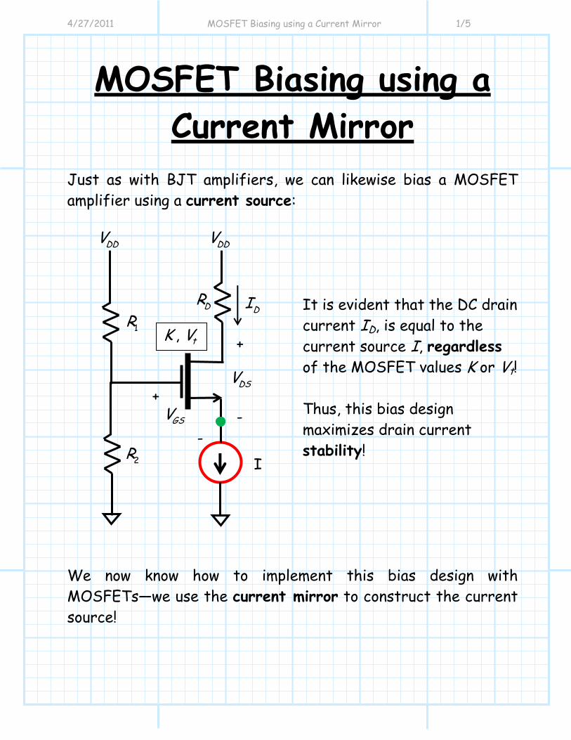
MOSFET Biasing using a Current Mirror
Just as with BJT amplifiers, we can likewise bias a MOSFET amplifier using a current source:
It is evident that the DC drain current ID, is equal to the current source I, regardless of the MOSFET values K or Vt! Thus, this bias design maximizes drain current stability!
We now know how to implement this bias design with MOSFETs—we use the current mirror to construct the current source!
, tK V 1R
2R
DR
DDV DDV
DI
+
DSV -
+ GSV
- I

4/27/2011 MOSFET Biasing using a Current Mirror 2/5
Since DI I= , it is evident that GSV must be equal to:
tGSIV VK
= +
and since the DC gate voltage is:
2
1 2G DD
RV VR R⎛ ⎞
= ⎜ ⎟+⎝ ⎠
It is evident that the DC source voltage SV is thus:
, tK V
Q1 Q2
DDV
1R
2R
DR
DDV
DI
+
DSV -
+ GSV
-
VDD
R I
+ VGS1 -
+ VGS2 -

4/27/2011 MOSFET Biasing using a Current Mirror 3/5
2
1 2
S G GS
tDD
V V VR IV V
R R K
= −
⎛ ⎞⎛ ⎞= − +⎜ ⎟⎜ ⎟+⎝ ⎠ ⎝ ⎠
Since we are biasing with a current source, we do not need to worry about drain current stability—the current source will determine the DC drain current for all conditions (i.e., DI I= ). We might conclude therefore, that we should make DC source voltage VS as small as possible. After all, this would allow us to maximize the output voltage swing (i.e., maximize D DI R and DSV ). Note however, that the source voltage SV of the MOSFET is numerically equal to the drain voltage 2DV (and thus 2DSV ) of the second MOSFET of the current mirror. Q: So what?! A: The voltage 2 SDSV V= must be greater than:
( )2 2 1 1
1
GS t GS t
tDD ref
V V V VV I R V
− = −
= − −
in order for the second MOSFET to remain in saturation. There is a minimum voltage across the current source in order for the current source to properly operate!

4/27/2011 MOSFET Biasing using a Current Mirror 4/5
Thus, to maximize output swing, we might wish to set:
1 1S GS tV V V= − (although to be practical, we should make SV slightly greater than this to allow for some design margin). Q: How do we “set” the DC source voltage SV ?? A: By setting the DC gate voltage GV !!
Recall that the DC voltage GSV is determined by the DC current source value I:
tGSIV VK
= +
and the DC gate voltage is determined by the two resistors
1 2 and R R :
2
1 2G DD
RV VR R⎛ ⎞
= ⎜ ⎟+⎝ ⎠
1R
2R
DR
DDV DDV
DI
+
DSV -
+ GSV
-
I + V > VGS1-Vt1
-
4/27/2011 MOSFET Biasing using a Current Mirror 5/5
Thus, we should select these resistors such that:
( )1 1
SG GS
t GS t
V V VI V V VK
= +
⎛ ⎞= + + −⎜ ⎟⎝ ⎠
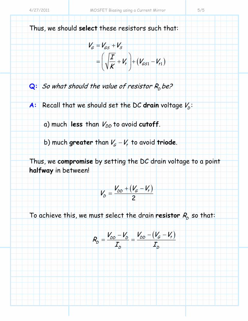
Q: So what should the value of resistor DR be? A: Recall that we should set the DC drain voltage DV :
a) much less than VDD to avoid cutoff.
b) much greater than tGV V− to avoid triode.
Thus, we compromise by setting the DC drain voltage to a point halfway in between!
( )2
tGDDD
V V VV
+ −=
To achieve this, we must select the drain resistor DR so that:
( )tGDDDD DD
D D
V V VV VRI I
− −−= =
4/27/2011 Example MOSFET Biasing using a Current Mirror 1/3
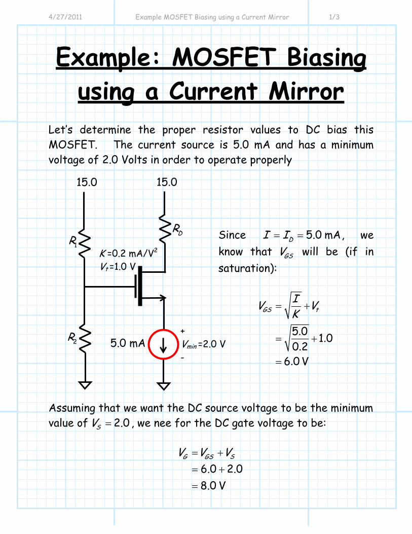
Example: MOSFET Biasing using a Current Mirror
Let’s determine the proper resistor values to DC bias this MOSFET. The current source is 5.0 mA and has a minimum voltage of 2.0 Volts in order to operate properly
Since 5.0 mADI I= = , we know that GSV will be (if in saturation):
. .
..
5 0 1 00 2
6 0 V
GS tIV VK
= +
= +
=
Assuming that we want the DC source voltage to be the minimum value of 2.0SV = , we nee for the DC gate voltage to be:
6.0 2.08.0 V
SG GSV V V= +
= +
=
1R
2R
DR
.15 0 .15 0
5.0 mA + Vmin =2.0 V -
K =0.2 mA/V2 Vt =1.0 V

4/27/2011 Example MOSFET Biasing using a Current Mirror 2/3
Thus, we need to select resistors 1 2 and R R so that:
. 2
1 2
8 0G DDRV V
R R⎛ ⎞
= = ⎜ ⎟+⎝ ⎠
or in other words, we want:
..
2
1 2
8 015 0
RR R⎛ ⎞
=⎜ ⎟+⎝ ⎠
Since we can make 1 2 and R R large, let’s assume that we want:
1 2 300KR R+ =
So that 1 140 KR = Ω and 2 160 KR = Ω . Finally, we want the DC drain voltage to be:
( )
( ). . .
.
215 0 8 0 1 0
211 0 V
DD G tD
V V VV + −=
+ −=
=
So that the resistor DR is:
. ..
.
15 0 11 05 0
0 8K
DD DD
D
V VRI−
=
−=
= Ω

4/27/2011 Example MOSFET Biasing using a Current Mirror 3/3
1 140KR =
.0 8KDR =
.15 0 .15 0
5.0 mA + Vmin =2.0 V -
K =0.2 mA/V2 Vt =1.0 V
2 160KR =