433 mhz Tx and Rx
8
DS337_2 June 01 ©2001 REG No 277 4001, England. Page 1 433MHz Narrow Band Radio Transmitter & Receivers Features • Miniature Module • FM Narrow Band Modulation • Optimal Range 400m • Operates Within 433 Licence Free Band • 34 Channels Available • Single Supply Voltage Applications • In Vehicle Telemetry Systems • Wireless Networking • Domestic And Commercial Wireless Security Systems • Panic Attack Facility Transmitter • Analogue And Digital Inputs • 10mw RF Output Power (100mw Optional) • Narrow Band Crystal Stabilised • Small Form Factor General Description The QBT37-XXX and QBR37-XXX are miniature narrow band transmitter and receiver UHF radio modules, which enable the implementation of a simple telemetry link at data rates up to 20Kbits/s. Available for operation between 433.075 and 434.725 MHz in 50KHz steps these modules give the possibility of 34 different frequency channels and are able to transmit at distances of up to 400m. Receiver • Data & Af Out • CD Implemented On Data Output • RSSI Output • Selective Ceramic If Filters The QBT37-XXX and QBR37-XXX modules will suit one-to-one and multi-node wireless links in applications including building and car security, remote industrial process monitoring and computer networking. Because of their small size and low power requirements, both modules are ideal for use in portable battery powered wireless applications
-
Upload
nair-krishna-raveendran -
Category
Documents
-
view
229 -
download
0
Transcript of 433 mhz Tx and Rx
8/7/2019 433 mhz Tx and Rx
http://slidepdf.com/reader/full/433-mhz-tx-and-rx 1/7
DS337_2 June 01 ©©2001 REG No 277 4001, England. Page 1
433MHz Narrow Band Radio Transmitter & Receivers
Features
• Miniature Module
• FM Narrow Band Modulation
• Optimal Range 400m
• Operates Within 433 Licence Free Band
• 34 Channels Available
• Single Supply Voltage
Applications
• In Vehicle Telemetry Systems
• Wireless Networking
• Domestic And Commercial Wireless SecuritySystems
• Panic Attack Facility
Transmitter• Analogue And Digital Inputs
• 10mw RF Output Power (100mw Optional)
• Narrow Band Crystal Stabilised
• Small Form Factor
General DescriptionThe QBT37-XXX and QBR37-XXX are miniaturenarrow band transmitter and receiver UHF radio
modules, which enable the implementation of asimple telemetry link at data rates up to 20Kbits/s.
Available for operation between 433.075 and434.725 MHz in 50KHz steps these modules givethe possibility of 34 different frequency channelsand are able to transmit at distances of up to400m.
Receiver
• Data & Af Out
• CD Implemented On Data Output
• RSSI Output
• Selective Ceramic If Filters
The QBT37-XXX and QBR37-XXX modules will
suit one-to-one and multi-node wireless links inapplications including building and car security,remote industrial process monitoring andcomputer networking. Because of their small sizeand low power requirements, both modules areideal for use in portable battery powered wirelessapplications

8/7/2019 433 mhz Tx and Rx
http://slidepdf.com/reader/full/433-mhz-tx-and-rx 2/7
DS337_2 June 01 ©©2001 REG No 277 4001, England. Page 2
433MHz Narrow Band Radio Transmitter & Receivers
Absolute Maximum Ratings: TransmitterOperating temperature: -10°C to +55°C
Storage temperature: -40°C to +100°C
Supply Voltage (pin 3) 10VData input (pin 5) 10V
Electrical Characteristics: Transmitter
pin min. typ. max. units notes
DC LEVELS
Supply voltage 4.5 5.0 5.5 Volts
Current & RF POWER
Supply current @ VCC = 5V (data low/high) 22 mA 1RF output power @ VCC = 5V 10 mW 1
RF & Data
Channel separation 50 KHzMax Modulation frequency 10 KHz
2nd
harmonic 66 dBc 1Harmonics @ > 1GHz 46 dBc 1Initial frequency accuracy 1 KHzOverall frequency accuracy 5 KHz
FM deviation (±) 7 KHz
Modulation bandwidth @ -3dB 10 KHzModulation distortion (THD) %Power up time to full RF 10 µs
Data rate 20000 bits/sData pulse width 50 10000 µs
Note 1: measured into a 50Ω impedance
8/7/2019 433 mhz Tx and Rx
http://slidepdf.com/reader/full/433-mhz-tx-and-rx 3/7
DS337_2 June 01 ©©2001 REG No 277 4001, England. Page 3
433MHz Narrow Band Radio Transmitter & Receivers
Absolute Maximum Ratings: ReceiverOperating temperature: -10°C to +55°C
Storage temperature: -40°C to +100°C
Supply Voltage 10VData input 10V
Electrical Characteristics: Receiver
pin min. typ. max. units notes
DC LEVELS Supply voltage 5 V
Supply current 14 mASupply ripple - - 10 mVP-P
Data output high =>4.5 VData output low <= 0.5 V
RF
RF sensitivity -107 DBmIF Bandwidth 40 KHzInitial frequency accuracy 1 KHzMax R.F. input -20 DBm
E.M.C.
Spurious responses upto 1GHz 36 dB
LO leakage, conducted 57 dBmLO leakage, radiated 57 dBm
DYNAMIC TIMING Power up to stable data (With RF signal present
5 mS
Signal to stable data (With power supply already on)
3 mS
Mark:space ratio 50 %Bit rate 20 20000 bps
8/7/2019 433 mhz Tx and Rx
http://slidepdf.com/reader/full/433-mhz-tx-and-rx 4/7
DS337_2 June 01 ©©2001 REG No 277 4001, England. Page 4
433MHz Narrow Band Radio Transmitter & Receivers
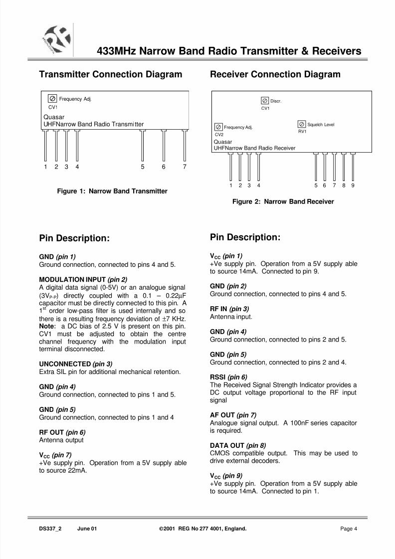
Transmitter Connection Diagram
QuasarUHFNarrow Band Radio Transmitter
1 2 3 4 5 6 7
CV1
Frequency Adj.
Figure 1: Narrow Band Transmitter
Pin Description:
GND (pin 1) Ground connection, connected to pins 4 and 5.
MODULATION INPUT (pin 2) A digital data signal (0-5V) or an analogue signal
(3VP-P) directly coupled with a 0.1 – 0.22µFcapacitor must be directly connected to this pin. A1
storder low-pass filter is used internally and so
there is a resulting frequency deviation of ±7 KHz.Note: a DC bias of 2.5 V is present on this pin.CV1 must be adjusted to obtain the centrechannel frequency with the modulation inputterminal disconnected.
UNCONNECTED (pin 3) Extra SIL pin for additional mechanical retention.
GND (pin 4) Ground connection, connected to pins 1 and 5.
GND (pin 5) Ground connection, connected to pins 1 and 4
RF OUT (pin 6) Antenna output
VCC (pin 7) +Ve supply pin. Operation from a 5V supply ableto source 22mA.
Receiver Connection Diagram
QuasarUHFNarrow Band Radio Receiver
1 2 3 4 5 6 7 8 9
CV1
CV2RV1
Frequency Adj.
Discr.
Squelch Level
Figure 2: Narrow Band Receiver
Pin Description:
VCC (pin 1) +Ve supply pin. Operation from a 5V supply ableto source 14mA. Connected to pin 9.
GND (pin 2)
Ground connection, connected to pins 4 and 5.
RF IN (pin 3) Antenna input.
GND (pin 4) Ground connection, connected to pins 2 and 5.
GND (pin 5) Ground connection, connected to pins 2 and 4.
RSSI (pin 6) The Received Signal Strength Indicator provides a
DC output voltage proportional to the RF inputsignal
AF OUT (pin 7) Analogue signal output. A 100nF series capacitoris required.
DATA OUT (pin 8) CMOS compatible output. This may be used todrive external decoders.
VCC (pin 9) +Ve supply pin. Operation from a 5V supply able
to source 14mA. Connected to pin 1.

8/7/2019 433 mhz Tx and Rx
http://slidepdf.com/reader/full/433-mhz-tx-and-rx 5/7
DS337_2 June 01 ©©2001 REG No 277 4001, England. Page 5
433MHz Narrow Band Radio Transmitter & Receivers
Functional DescriptionThe QBT37-XXX FM narrow band transmittermodule consists of a low frequency directlymodulated crystal oscillator and multiplier andfilter circuits. Baseband data directly modulatesthe low frequency crystal oscillator, the output ofwhich is applied to the first of three frequencymultipliers to achieve the final output frequencyafter being processed by interstage band passfilter circuits.
The QBR37-XXX FM narrow band receivermodule uses the single conversion super-hetprinciple. The applied RF signal is amplified andapplied to the RF mixer. Using a 10.7 MHz IFfrequency at 50KHz channel spacing enables useof ceramic filters to provide good adjacent channelrejection. Baseband demodulation is recoveredfrom this IF and applied to a squelch circuit.Therefore, data is only available when a RF signalis present.
Q1 Q2 Q3 Q4
X1
D1CV1.FREQ.ADJ.
10k ΩΩ
470pF100kΩΩ
100kΩΩ
15kΩΩ
AUX
1 2 3 4
3V ANALOGUE MODULATION
0.1 µµF
5V
0V
DIGITAL MODULATION
2.5VDC +5V
RF OUTPUTZ = 50ΩΩ
5 6 7
+5V
X1 XF1 XF2
CV2FREQ.
Q1
Q2 Q3
+5V RF ANT 50ΩΩ
RSSI
+5V IF
100mV
5V
0V
ANALOGUE OUTPUT
DIGITAL OUTPUT20Hz - 10KHz
22KΩΩ
0.1µµ F
1 2 3 4 5 6 7 8 9
IC1+5V
+5V
Figure 3: Narrow Band Transmitter andReceiver Block Diagrams
Frequency ChannelsThe QBT37-XXX and QBR37-XXX are availablein 34 discrete frequency channels from 433.075 to434.725 MHz in 50KHz steps. The table belowshows the list of possible frequency channels.
CH. FREQ/MHz CH. FREQ/MHz
1 433.075 18 433.9252 433.125 19 433.9753 433.175 20 434.0254 433.225 21 434.075 (1)5 433.275 22 434.1256 433.325 23 434.1757 433.375 24 434.225
8 433.425 25 434.2759 433.475 26 434.325 (1)
10 433.525 27 434.37511 433.575 28 434.42512 433.625 29 434.47513 433.675 30 434.525 (1)14 433.725 31 434.57515 433.775 32 434.62516 433.825 33 434.67517 433.875 34 434.725
(1) Stock Item
8/7/2019 433 mhz Tx and Rx
http://slidepdf.com/reader/full/433-mhz-tx-and-rx 6/7
DS337_2 June 01 ©©2001 REG No 277 4001, England. Page 6
433MHz Narrow Band Radio Transmitter & Receivers
Antenna DesignThe design and positioning of the antenna is ascrucial as the module performance itself inachieving a good wireless system range. Thefollowing will assist the designer in maximisingsystem performance.
The antenna should be kept as far away fromsources of electrical interference as physicallypossible. If necessary, additional power linedecoupling capacitors should be placed close tothe module.
The antenna ‘hot end’ should be kept clear of anyobjects, especially any metal as this can severelyrestrict the efficiency of the antenna to receivepower. Any earth planes restricting the radiationpath to the antenna will also have the same effect.
Best range is achieved with either a straight pieceof wire, rod or PCB track @ ¼ wavelength(15.5cm @ 433.92MHz). Further range may beachieved if the ¼ wave antenna is placedperpendicular in the middle of a solid earth planemeasuring at least 16cm radius. In this case, theantenna should be connected to the module viasome 50 ohm characteristic impedance coax
RF
RF
Helical Antenna
Whip Antenna
34mm @ 433MHz
17 turns equally spaced∅
= 5mm (inside)
15.5cm @ 433MHz
Figure 4: Antenna Configurations To Be UsedWith The FM Narrow Band Transmitter &
Receiver Modules
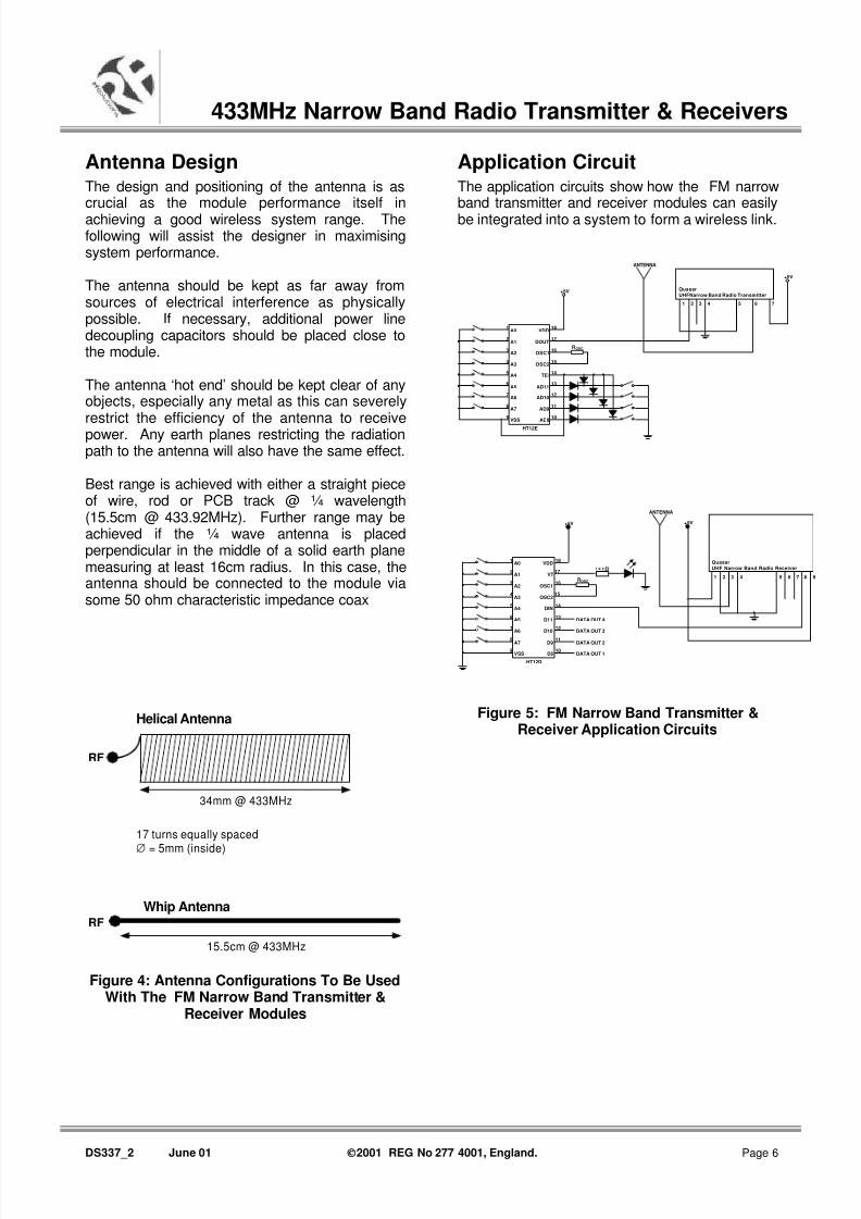
Application CircuitThe application circuits show how the FM narrowband transmitter and receiver modules can easilybe integrated into a system to form a wireless link.
QuasarUHFNarrow Band Radio Transmitter
A0
A1
A2
A3
A4
A5
A6
A7
VSS AD8
AD9
AD10
AD11
TE\
OSC2
OSC1
DOUT
VDD1
2
3
4
5
6
7
8
9 10
11
12
13
14
15
16
17
18
HT12E
ROSC
+5V
4 51 2 3
+5V
ANTENNA
6 7
A0
A1
A2
A3
A4
A5
A6
A7
VSS D8
D9
D10
D11
DIN
OSC2
OSC1
VT
VDD1
2
3
4
5
6
7
8
9 10
11
12
13
14
16
18
HT12D
+5V
15
ROSC
DATA OUT 1
DATA OUT 2
DATA OUT 3
DATA OUT 4
171 K 5 ΩΩ
QuasarUHF Narrow Band Radio Receiver
1 2 3 4 5 6 7
+5V
ANTENNA
8 9
Figure 5: FM Narrow Band Transmitter &Receiver Application Circuits

8/7/2019 433 mhz Tx and Rx
http://slidepdf.com/reader/full/433-mhz-tx-and-rx 7/7
DS337_2 June 01 ©©2001 REG No 277 4001, England. Page 7
433MHz Narrow Band Radio Transmitter & Receivers
Mechanical Dimensions
QuasarUHFNarrow Band Radio Transmitter
1 2 3 4 5 6 7
17.78mm
41.9mm
11.68mm
2.54mm 5.08mm
7mm
pin Dia is max 0.75mm. recommended mounting hole diameter is 1mm
QuasarUHFNarrow Band Radio Receiver
1 2 3 4 5 6 7 8 9
17.78mm
pin spacing 2.54mm
50mm
21mm
7.5mm
6.5mm 6.5mm
Figure 6: FM Narrow Band Transmitter and Receiver
Ordering InformationStandard Product;
Part No Description
QBT37-434.075 SIL Narrow Band Transmitter
QBT37-434.325 SIL Narrow Band TransmitterQBT37-434.525 SIL Narrow Band Transmitter
QBR37-434.075 SIL Narrow Band ReceiverQBR37-434.325 SIL Narrow Band ReceiverQBR37-434.525 SIL Narrow Band Receiver
Custom Product;Any frequency between 433.075MHz – 434.725MHz is available in steps of 50KHz.This gives 34 channels of module possibility.Please consult our sales department for further information.
R F Solutions Ltd.,
Unit 21, Cliffe Industrial Estate,
South Street, Lewes,
E. Sussex. BN8 6JL, England
Tel: +44 (0)1273 898 000 Fax: +44 (0)1273 480 661
Email : [email protected] http://www.rfsolutions.co.uk
Information contained in this document is believed to be accurate , however no representation or warranty is given and no liability is assumed by R.F. Solutions Ltd. Withrespect to the accuracy of such information. Use of R.F.Solutions as critical components in life support systems is not authorised except with express written approval from R.F.Solutions Ltd.