40 W (46 dBm), 9 GHz to 10.5 GHz, GaN Power Amplifier Data ... · 40 W (46 dBm), 9 GHz to 10.5 GHz,...
23
40 W (46 dBm), 9 GHz to 10.5 GHz, GaN Power Amplifier Data Sheet HMC8415LP6GE Rev. A Document Feedback Information furnished by Analog Devices is believed to be accurate and reliable. However, no responsibility is assumed by Analog Devices for its use, nor for any infringements of patents or other rights of third parties that may result from its use. Specifications subject to change without notice. No license is granted by implication or otherwise under any patent or patent rights of Analog Devices. Trademarks and registered trademarks are the property of their respective owners. One Technology Way, P.O. Box 9106, Norwood, MA 02062-9106, U.S.A. Tel: 781.329.4700 ©2018–2019 Analog Devices, Inc. All rights reserved. Technical Support www.analog.com FEATURES High output power: 46 dBm typical at PIN = 23 dBm High small signal gain: 32.5 dB typical High power gain: 23 dB typical at PIN = 23 dBm Frequency range: 9 GHz to 10.5 GHz High power added efficiency: 40% typical at PIN = 23 dBm Supply voltage: VDDxA/VDDxB = 28 V at 1000 mA 6 mm × 6 mm, 40-lead LFSCP APPLICATIONS Weather radars Marine radars Military radars FUNCTIONAL BLOCK DIAGRAM GND HMC8415LP6GE GND PACKAGE BASE RFOUT GND GND RFIN GND V GG1B V GG2B V GG3B V DD1B V DD2B V DD3B V DD3B V GG1A V GG2A V GG3A V DD1A V DD2A V DD3A V DD3A 16688-001 Figure 1. GENERAL DESCRIPTION The HMC8415LP6GE is a gallium nitride (GaN), power amplifier, delivering 40 W (46 dBm) with more than 37.5% power added efficiency (PAE) across a bandwidth of 9 GHz to 10.5 GHz. The HMC8415LP6GE is ideal for pulsed applications, such as wireless weather, marine, and military radar applications.
Transcript of 40 W (46 dBm), 9 GHz to 10.5 GHz, GaN Power Amplifier Data ... · 40 W (46 dBm), 9 GHz to 10.5 GHz,...

40 W (46 dBm), 9 GHz to 10.5 GHz, GaN Power Amplifier
Data Sheet HMC8415LP6GE
Rev. A Document Feedback Information furnished by Analog Devices is believed to be accurate and reliable. However, no responsibility is assumed by Analog Devices for its use, nor for any infringements of patents or other rights of third parties that may result from its use. Specifications subject to change without notice. No license is granted by implication or otherwise under any patent or patent rights of Analog Devices. Trademarks and registered trademarks are the property of their respective owners.
One Technology Way, P.O. Box 9106, Norwood, MA 02062-9106, U.S.A. Tel: 781.329.4700 ©2018–2019 Analog Devices, Inc. All rights reserved. Technical Support www.analog.com
FEATURES High output power: 46 dBm typical at PIN = 23 dBm High small signal gain: 32.5 dB typical High power gain: 23 dB typical at PIN = 23 dBm Frequency range: 9 GHz to 10.5 GHz High power added efficiency: 40% typical at PIN = 23 dBm Supply voltage: VDDxA/VDDxB = 28 V at 1000 mA 6 mm × 6 mm, 40-lead LFSCP
APPLICATIONS Weather radars Marine radars Military radars
FUNCTIONAL BLOCK DIAGRAM
GNDHMC8415LP6GE
GND
PACKAGEBASE
RFOUTGND
GNDRFINGND
V GG
1B
V GG
2B
V GG
3B
V DD1
BV D
D2B
V DD3
B
V DD3
B
V GG
1A
V GG
2 A
V GG
3A
V DD1
AV D
D2A
V DD3
A
V DD3
A
1668
8-00
1
Figure 1.
GENERAL DESCRIPTION The HMC8415LP6GE is a gallium nitride (GaN), power amplifier, delivering 40 W (46 dBm) with more than 37.5% power added efficiency (PAE) across a bandwidth of 9 GHz to 10.5 GHz.
The HMC8415LP6GE is ideal for pulsed applications, such as wireless weather, marine, and military radar applications.

HMC8415LP6GE Data Sheet
Rev. A | Page 2 of 23
TABLE OF CONTENTS Features .............................................................................................. 1 Applications ....................................................................................... 1 Functional Block Diagram .............................................................. 1 General Description ......................................................................... 1 Revision History ............................................................................... 2 Specifications ..................................................................................... 3
Electrical Specifications ............................................................... 3 Total Target Quiescent Current by VDDxA/VDDxB ....................... 4
Absolute Maximum Ratings ............................................................ 5 Thermal Resistance ...................................................................... 5 ESD Caution .................................................................................. 5
Pin Configuration and Function Descriptions ............................. 6 Interface Schematics..................................................................... 7
Typical Performance Characteristics ..............................................8 Theory of Operation ...................................................................... 14 Applications Information .............................................................. 15
Typical Application Circuit and Pulsor Circuit ..................... 17 Using the EV1HMC8415LP6G with the Drain Bias Pulsor Board ................................................................................................ 19
Recommended Bias Sequence .................................................. 20 Making Average to Pulsed Approximations ............................... 21 Evaluation PCB ............................................................................... 22
Bill of Materials ........................................................................... 22 Outline Dimensions ....................................................................... 23
Ordering Guide .......................................................................... 23
REVISION HISTORY 4/2019—Rev. 0 to Rev. A Change to Table 5 ............................................................................. 5 Updated Outline Dimensions ....................................................... 23 Changes to Ordering Guide .......................................................... 23 9/2018—Revision 0: Initial Version

Data Sheet HMC8415LP6GE
Rev. A | Page 3 of 23
SPECIFICATIONS ELECTRICAL SPECIFICATIONS TA = 25°C, VDDxA/VDDxB = 28 V, target quiescent current (IDQ) = 1000 mA, drain bias pulse width = 100 µs, 10% duty cycle, and the frequency range = 9 GHz to 10 GHz, unless otherwise noted.
Table 1. Parameter Symbol Min Typ Max Unit Test Conditions/Comments FREQUENCY RANGE 9 10 GHz GAIN
Small Signal 30 32.5 dB Small Signal Flatness 1 dB Power Gain 23 dB Input power (PIN) = 23 dBm 24 dB PIN = 21 dBm
RETURN LOSS Input 20 dB Output 10 dB
POWER Output Power POUT 46 dBm PIN = 23 dBm 45 dBm PIN = 21 dBm Power Added Efficiency PAE 40 % PIN = 23 dBm 37.5 % PIN = 21 dBm
TARGET QUIESCENT CURRENT IDQ 1000 mA Adjust the VGG (VGGxA/VGGxB) between −4.0 V and −1.5 V to achieve an IDQ = 1000 mA typical, VGG (VGGxA/VGGxB) = −2.5 V typical to achieve IDQ = 1000 mA
TA = 25°C, VDDxA/VDDxB = 28 V, IDQ = 1000 mA, drain bias pulse width = 100 µs, 10% duty cycle, and the frequency range = 10 GHz to 10.5 GHz, unless otherwise noted.
Table 2. Parameter Symbol Min Typ Max Unit Test Conditions/Comments FREQUENCY RANGE 10 10.5 GHz GAIN
Small Signal 25.5 28 dB Small Signal Flatness 5 dB Power Gain 22 dB PIN = 23 dBm 23.5 dB PIN = 21 dBm
RETURN LOSS Input 17 dB Output 8 dB
POWER Output Power POUT 45 dBm PIN = 23 dBm 44.5 dBm PIN = 21 dBm Power Added Efficiency PAE 37.5 % PIN = 23 dBm 37.5 % PIN = 21 dBm
TARGET QUIESCENT CURRENT IDQ 1000 mA Adjust the VGG (VGGxA/VGGxB) between −4.0 V and −1.5 V to achieve an IDQ = 1000 mA typical, VGG (VGGxA/VGGxB) = −2.5 V typical to achieve IDQ = 1000 mA

HMC8415LP6GE Data Sheet
Rev. A | Page 4 of 23
TOTAL TARGET QUIESCENT CURRENT BY VDDxA/VDDxB
Table 3. Parameter Symbol Min Typ Max Unit Test Conditions/Comments TARGET QUIESCENT CURRENT IDQ Adjust the VGG (VGGxA/VGGxB) from −4.0 V to −1.5 V to achieve an
IDQ = 1000 mA typical VDDxA/VDDxB = 24 V 1000 mA VDDxA/VDDxB = 28 V 1000 mA VDDxA/VDDxB = 32 V 1000 mA

Data Sheet HMC8415LP6GE
Rev. A | Page 5 of 23
ABSOLUTE MAXIMUM RATINGS Table 4. Parameter Rating Bias Voltage
Drain (VDDxA/VDDxB) 35 V dc Gate (VGGxA/VGGxB) −8 V dc to −1 V dc
Radio Frequency Input Power (RFIN) 30 dBm Maximum Drain Bias
Pulse Width (PW) 500 µs Duty Cycle 20%
Maximum Pulsed Power Dissipation, PDISS (TBASE = 85°C, Derate 752 mW/°C Above 85°C), Drain Bias Pulse Width = 200 µs at 20% Duty Cycle
105.3 W
Nominal Pulsed Peak Channel Temperature, Drain Bias Pulse Width = 200 µs at 20% Duty Cycle, PIN = 23 dBm, PDISS = 58 W at 9.0 GHz
162°C
Maximum Channel Temperature 225°C Maximum Peak Reflow Temperature for
Moisture Sensitivity Level 3 (MSL3)1 260°C
Storage Temperature Range −65°C to +150°C Operating Temperature Range −40°C to +85°C Electrostatic Discharge (ESD) Sensitivity
Human Body Model (HBM) Class 1A, Passed 250 V
1 See the Ordering Guide section for additional information.
Stresses at or above those listed under Absolute Maximum Ratings may cause permanent damage to the product. This is a stress rating only; functional operation of the product at these or any other conditions above those indicated in the operational section of this specification is not implied. Operation beyond the maximum operating conditions for extended periods may affect product reliability.
THERMAL RESISTANCE Thermal performance is directly linked to printed circuit board (PCB) design and operating environment. Careful attention to PCB thermal design is required.
θJC is the junction to case thermal resistance.
Table 5. Thermal Resistance Package Type1, 2 θJC Unit CP-40-7 1.33 °C/W
1 The thermal resistance (θJC) was determined by measuring θJC under the following conditions: the heat transfer is due solely to the thermal conduction from the channel through the ground pad to the PCB, and the ground pad is held constant at the operating temperature of 85°C.
2 Drain bias pulse width = 200 µs at 20% duty cycle.
ESD CAUTION

HMC8415LP6GE Data Sheet
Rev. A | Page 6 of 23
PIN CONFIGURATION AND FUNCTION DESCRIPTIONS
1
34
2NICNICNIC
GND56
RFINGND
7NIC8NIC9NIC
21 NIC22 NIC
11V G
G1B
12V G
G2B
13
V GG
3B
14
NIC
15
V DD1
B
16
V DD2
B
17
NIC
18
NIC
19
V DD3
B
20
V DD3
B
31
V DD3
A
HMC8415LP6GETOP VIEW
(Not to Scale)
23 NIC24 NIC25 GND26 RFOUT27 GND28 NIC29 NIC30 NIC
NOTES1. NIC = NO INTERNAL CONNECTION.2. EXPOSED PAD. THE EXPOSED PAD MUST BE CONNECTED TO RF AND DC GROUND.
10NIC
32
V DD3
A
33
NIC
34
NIC
35
V DD2
A
36
V DD1
A
37
NIC
38
V GG
3A
39
V GG
2A
40
V GG
1A
1668
8-00
2
Figure 2. Pin Configuration
Table 6. Pin Function Descriptions Pin No. Mnemonic Description 1 to 3, 7 to 10, 14, 17, 18, 21 to 24,
28 to 30, 33, 34, 37 NIC No Internal Connection. These pins must be connected to RF and dc ground.
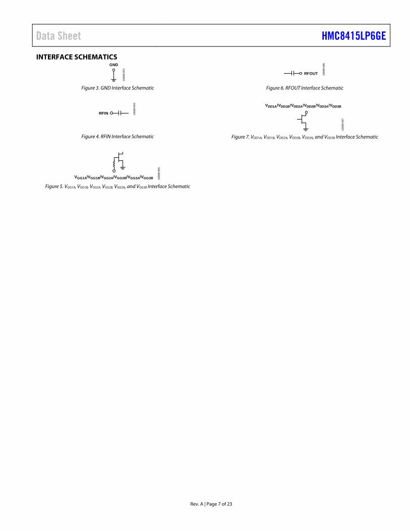
4, 6, 25, 27 GND Ground. These pins must be connected to RF and dc ground. See Figure 3 for the GND interface schematic.
5 RFIN RF Input. This pin is ac-coupled and matched to 50 Ω. See Figure 4 for the RFIN interface schematic.
11 to13, 38 to 40 VGG1B, VGG2B, VGG3B, VGG1A, VGG2A, VGG3A
Gate Control Voltage Pins. External bypass capacitors of 1 µF, 100 pF, and 2.2 nF are required. See Figure 5 for the VGG1B, VGG2B, VGG3B, VGG1A, VGG2A, and VGG3A interface schematic.
15, 16, 19, 20, 31, 32, 35, 36 VDD1B, VDD2B, VDD3B, VDD1A, VDD2A, VDD3A
Drain Bias Pins for the Amplifier. External bypass capacitors of 1 nF and 3.3 Ω resistors are required. See Figure 7 for the VDD1B, VDD2B, VDD3B, VDD1A, VDD2A, and VDD3A interface schematic.
26 RFOUT RF Output. This pin is ac-coupled and matched to 50 Ω. See Figure 6 for the RFOUT interface schematic.
EPAD Exposed Pad. The exposed pad must be connected to RF and dc ground.
Data Sheet HMC8415LP6GE
Rev. A | Page 7 of 23
INTERFACE SCHEMATICS GND
1668
8-00
3
Figure 3. GND Interface Schematic
RFIN 1668
8-00
4
Figure 4. RFIN Interface Schematic
VGG1A/VGG1B/VGG2A/VGG2B/VGG3A/VGG3B 1668
8-00
5
Figure 5. VGG1A, VGG1B, VGG2A, VGG2B, VGG3A, and VGG3B Interface Schematic
RFOUT 1668
8-00
6
Figure 6. RFOUT Interface Schematic
VDD1A/VDD1B/VDD2A/VDD2B/VDD3A/VDD3B
1668
8-00
7
Figure 7. VDD1A, VDD1B, VDD2A, VDD2B, VDD3A, and VDD3B Interface Schematic

HMC8415LP6GE Data Sheet
Rev. A | Page 8 of 23
TYPICAL PERFORMANCE CHARACTERISTICS
–30
–20
–10
0
10
20
30
40
8.5 9.0 9.5 10.0 10.5 11.0
RESP
ONS
E (d
B)
FREQUENCY (GHz) 1668
8-00
8
SMALL SIGNAL GAINOUTPUT RETURN LOSSINPUT RETURN LOSS
Figure 8. Small Signal Gain and Return Loss (Response) vs. Frequency
–30
–25
–20
–15
–10
–5
0
8.5 9.0 9.5 10.0 10.5 11.0
INPU
T RE
TURN
LO
SS (d
B)
FREQUENCY (GHz)
–40°C +25°C +85°C
1668
8-00
9
Figure 9. Input Return Loss vs. Frequency at Various Temperatures
10
15
20
25
30
35
40
8.5 9.0 9.5 10.0 10.5 11.0
SMAL
L SI
GNA
L G
AIN
(dB)
FREQUENCY (GHz)
24V28V32V
1668
8-01
0
Figure 10. Small Signal Gain vs. Frequency at Various Supply Voltages at
IDQ = 1000 mA
8.5 9.0 9.5 10.0 10.5 11.0FREQUENCY (GHz)
10
15
20
25
30
35
40
SMAL
L SI
GNA
L G
AIN
(dB)
–40°C +25°C +85°C
1668
8-01
1
Figure 11. Small Signal Gain vs. Frequency at Various Temperatures
8.5 9.0 9.5 10.0 10.5 11.0FREQUENCY (GHz)
–25
–20
–15
–10
–5
0
OUT
PUT
RETU
RN L
OSS
(dB)
–40°C +25°C +85°C
1668
8-01
2
Figure 12. Output Return Loss vs. Frequency at Various Temperatures
8.5 9.0 9.5 10.0 10.5 11.0FREQUENCY (GHz)
10
15
20
25
30
35
40
SMAL
L SI
GNA
L G
AIN
(dB)
1000mA500mA200mA
1668
8-01
3
Figure 13. Small Signal Gain vs. Frequency at Various Quiescent Currents at
VDDxA/VDDxB = 28 V

Data Sheet HMC8415LP6GE
Rev. A | Page 9 of 23
30
32
34
36
38
40
42
44
46
48
8.5 9.0 9.5 10.0 11.010.5
P OUT
(dBm
)
FREQUENCY (GHz)
25dBm23dBm21dBm19dBm17dBm15dBm
1668
8-01
4
Figure 14. Output Power (POUT) vs. Frequency at Various Input Power (PIN) Levels
8.5 9.0 9.5 10.0 11.010.5FREQUENCY (GHz)
30
32
34
36
38
40
42
44
46
50
48
P OUT
(dBm
)
–40°C +25°C +85°C
1668
8-01
5
Figure 15. POUT vs. Frequency at Various Temperatures at PIN = 23 dBm
8.5 9.0 9.5 10.0 10.5 11.0
P OUT
(dBm
)
FREQUENCY (GHz)
30
32
34
36
38
40
42
44
46
50
48
1668
8-01
6
24V28V32V
Figure 16. POUT at PIN = 23 dBm vs. Frequency at Various Supply Voltages at
IDQ = 1000 mA
8.5 9.0 9.5 10.0 11.010.5FREQUENCY (GHz)
0
5
10
15
20
25
30
35
40
50
45
POW
ERAD
DED
EFFI
CIEN
CY
(%)
25dBm23dBm21dBm19dBm17dBm15dBm
1668
8-01
7
Figure 17. Power Added Efficiency vs. Frequency at Various PIN Levels
8.5 9.0 9.5 10.0 11.010.5FREQUENCY (GHz)
30
32
34
36
38
40
42
44
46
50
48
–40°C +25°C +85°C
P OUT
(dBm
)
1668
8-01
8
Figure 18. POUT vs. Frequency at Various Temperatures at PIN = 21 dBm
8.5 9.0 9.5 10.0 11.010.5FREQUENCY (GHz)
30
32
34
36
38
40
42
44
46
48
P OUT
(dBm
)
24V28V32V
1668
8-01
9
Figure 19. POUT at PIN = 21 dBm vs. Frequency at Various Supply Voltages at
IDQ = 1000 mA

HMC8415LP6GE Data Sheet
Rev. A | Page 10 of 23
8.5 9.0 9.5 10.0 11.010.5
P OUT
(dBm
)
FREQUENCY (GHz)
30
32
34
36
38
40
42
44
46
50
48
1668
8-02
0
1000mA500mA300mA
Figure 20. POUT at PIN = 23 dBm vs. Frequency at Various Quiescent Currents
at VDDxA/VDDxB = 28 V
8.5 9.0 9.5 10.0 11.010.5FREQUENCY (GHz)
0
10
20
30
40
50
60
POW
ERAD
DED
EFFI
CIEN
CY
(%)
–40°C +25°C +85°C
1668
8-02
1
Figure 21. Power Added Efficiency at PIN = 23 dBm vs. Frequency at Various
Temperatures
8.5 9.0 9.5 10.0 11.010.5FREQUENCY (GHz)
0
5
10
15
20
25
30
35
40
45
50
POW
ERAD
DED
EFFI
CIEN
CY
(%)
1668
8-02
2
24V28V32V
Figure 22. Power Added Efficiency at PIN = 23 dBm vs. Frequency at Various
Supply Voltages at IDQ = 1000 mA
8.5 9.0 9.5 10.0 11.010.5FREQUENCY (GHz)
30
32
34
36
38
40
42
44
46
50
48
P OUT
(dBm
)
1668
8-02
3
1000mA500mA300mA
Figure 23. POUT at PIN = 21 dBm vs. Frequency at Various Quiescent Currents
at VDDxA/VDDxB = 28 V
POW
ERAD
DED
EFFI
CIEN
CY
(%)
8.5 9.0 9.5 10.0 11.010.5FREQUENCY (GHz) 16
688-
0240
10
20
30
40
50
60 –40°C +25°C +85°C
Figure 24. Power Added Efficiency at PIN = 21 dBm vs. Frequency at Various
Temperatures
0
5
10
15
20
25
30
35
40
45
50
8.5 9.0 9.5 10.0 11.010.5
POW
ERAD
DED
EFFI
CIEN
CY
(%)
FREQUENCY (GHz) 1668
8-02
5
24V28V32V
Figure 25. Power Added Efficiency at PIN = 21 dBm vs. Frequency at Various
Supply Voltages at IDQ = 1000 mA

Data Sheet HMC8415LP6GE
Rev. A | Page 11 of 23
0
5
10
15
20
25
30
35
40
45
50
8.5 9.0 9.5 10.0 10.5 11.0
POW
ERAD
DED
EFFI
CIEN
CY
(%)
FREQUENCY (GHz)
1000mA500mA200mA
1668
8-02
6
Figure 26. Power Added Efficiency at PIN = 23 dBm vs. Frequency at Various
Quiescent Currents, VDDxA/VDDxB = 28 V
FREQUENCY (GHz)
0
1000
2000
3000
4000
5000
0
10
20
30
40
50I D
D (m
A)
POW
ER G
AIN
(dB)
, PO
UT (d
Bm),
PAE
(%)
8.5 9.0 9.5 10.0 10.5 11.0
1668
8-02
7
500
1500
2500
3500
4500
POWER GAINPOUTPAEIDD
Figure 27. Power Gain, POUT, PAE, and Supply Current (IDD) vs. Frequency at
PIN = 23 dBm
30
32
34
36
38
40
42
44
46
50
48
P OUT
(dBm
)
8.5 9.0 9.5 10.0 11.010.5FREQUENCY (GHz)
PW = 20µs, DC = 2%PW = 50µs, DC = 5%PW = 100µs, DC = 10%PW = 200µs, DC = 20%PW = 1000µs, DC = 20%
1668
8-02
8
Figure 28. POUT vs. Frequency at Various Pulse Widths (PW) and Duty Cycles
(DC) at PIN = 23 dBm
0
5
10
15
20
25
30
35
40
45
50
8.5 9.0 9.5 10.0 11.010.5
POW
ERAD
DED
EFFI
CIEN
CY
(%)
FREQUENCY (GHz) 1668
8-02
9
1000mA300mA500mA
Figure 29. Power Added Efficiency at PIN = 21 dBm vs. Frequency at Various
Quiescent Currents, VDDxA/VDDxB = 28V
FREQUENCY (GHz)
0
1000
2000
3000
4000
5000
0
10
20
30
40
50
I DD
(mA)
POW
ER G
AIN
(dB)
, PO
UT (d
Bm),
PAE
(%)
8.5 9.0 9.5 10.0 10.5 11.0
1668
8-03
0
500
1500
2500
3500
4500
5
15
25
35
45
POWER GAINPOUTPAEIDD
Figure 30. Power Gain, POUT, PAE, and IDD vs. Frequency at PIN = 21 dBm
30
32
34
36
38
40
42
44
46
50
48
8.5 9.0 9.5 10.0 11.010.5
P OUT
(dBm
)
FREQUENCY (GHz) 1668
8-03
1
PW = 20µs, DC = 2%PW = 50µs, DC = 5%PW = 100µs, DC = 10%PW = 200µs, DC = 20%PW = 1000µs, DC = 20%
Figure 31. POUT vs. Frequency at Various Pulse Widths (PW) and Duty Cycles
(DC) at PIN = 21 dBm

HMC8415LP6GE Data Sheet
Rev. A | Page 12 of 23
0
5
10
15
20
25
30
35
40
50
45
8.5 9.0 9.5 10.0 11.010.5
POW
ERAD
DED
EFFI
CIEN
CY
(%)
FREQUENCY (GHz)
PW = 20µs, DC = 2%PW = 50µs, DC = 5%PW = 100µs, DC = 10%PW = 200µs, DC = 20%PW = 1000µs, DC = 20%
1668
8-03
2
Figure 32. Power Added Efficiency vs. Frequency at Various Pulse Widths (PW)
and Duty Cycles (DC) at PIN = 23 dBm
0
5
10
15
20
25
30
35
40
50
45
0
500
1000
1500
2000
2500
3000
3500
4000
5000
4500
P OUT
(dBm
), PO
WER
GAI
N (d
B),P
AE (%
)
I DD
(mA)
INPUT POWER (dBm) 1668
8-03
3
5 7 9 11 13 15 17 19 21 23 25 27
POUTPOWER GAINPAEIDD
Figure 33. POUT, Power Gain, PAE, and IDD vs. Input Power at 9.0 GHz
P OUT
(dBm
), PO
WER
GAI
N (d
B),P
AE (%
)
I DD
(mA)
1668
8-03
40
500
1000
1500
2000
2500
3000
3500
4000
4500
5000
0
5
10
15
20
25
30
35
40
45
50
5 7 9 11 13 15 17 19 21 23 25 27INPUT POWER (dBm)
POUTPOWER GAINPAEIDD
Figure 34. POUT, Power Gain, PAE, and IDD vs. Input Power at 10 GHz
1668
8-03
50
5
10
15
20
25
30
35
40
45
50
8.50 8.75 9.00 9.25 9.50 9.75 10.00 10.25 10.50 10.75 11.00
POW
ERAD
DED
EFFI
CIEN
CY
(%)
FREQUENCY (GHz)
PW = 20µs, DC = 2%PW = 50µs, DC = 5%PW = 100µs, DC = 10%PW = 200µs, DC = 20%PW = 1000µs, DC = 20%
Figure 35. Power Added Efficiency vs. Frequency at Various Pulse Widths (PW)
and Duty Cycles (DC) at PIN = 21 dBm
P OUT
(dBm
), PO
WER
GAI
N (d
B),P
AE (%
)
1668
8-03
60
500
1000
1500
2000
2500
3000
3500
4000
4500
5000
0
5
10
15
20
25
30
35
40
45
50
5 7 9 11 13 15 17 19 21 23 25 27
I DD
(mA)
INPUT POWER (dBm)
POUTPOWER GAINPAEIDD
Figure 36. POUT, Power Gain, PAE, and IDD vs. Input Power at 9.5 GHz
0
5
10
15
20
25
30
35
40
50
45
0
500
1000
1500
2000
2500
3000
3500
4000
5000
4500
P OUT
(dBm
), PO
WER
GAI
N (d
B),P
AE (%
)
I DD
(mA)
1668
8-03
7
5 7 9 11 13 15 17 19 21 23 25 27INPUT POWER (dBm)
POUTPOWER GAINPAEIDD
Figure 37. POUT, Power Gain, PAE, and IDD vs. Input Power at 10.5 GHz

Data Sheet HMC8415LP6GE
Rev. A | Page 13 of 23
0
20
40
60
80
100
120
5.0 7.5 10.0 12.5 15.0 17.5 20.0 22.5 25.0 27.5 30.0
POW
ER D
ISSI
PATI
ON
(W)
INPUT POWER (dBm)
9GHz9.3GHz9.5GHz9.8GHz10GHz10.3GHz10.5GHz
1668
8-13
8
Figure 38. Power Dissipation vs. Input Power, Drain Bias Pulse Width = 100 µs
at 10% Duty Cycle
0
20
40
60
80
100
120
5.0 7.5 10.0 12.5 15.0 17.5 20.0 22.5 25.0 27.5 30.0
POW
ER D
ISSI
PATI
ON
(W)
INPUT POWER (dBm)
9GHz9.3GHz9.5GHz9.8GHz10GHz10.3GHz10.5GHz
1668
8-13
9
Figure 39. Power Dissipation vs. Input Power, Drain Bias Pulse Width = 20 µs
at 2% Duty Cycle
0
20
40
60
80
100
120
5.0 7.5 10.0 12.5 15.0 17.5 20.0 22.5 25.0 27.5 30.0
POW
ER D
ISSI
PATI
ON
(W)
INPUT POWER (dBm)
9GHz9.3GHz9.5GHz9.8GHz10GHz10.3GHz10.5GHz
1668
8-14
0
Figure 40. Power Dissipation vs. Input Power, Drain Bias Pulse Width = 50 µs at 5% Duty Cycle
0
20
40
60
80
100
120
5.0 7.5 10.0 12.5 15.0 17.5 20.0 22.5 25.0 27.5 30.0
POW
ER D
ISSI
PATI
ON
(W)
INPUT POWER (dBm)
MAXIMUM PDISS AT 85°C
9GHz9.3GHz9.5GHz9.8GHz10GHz10.3GHz10.5GHz
1668
8-14
1
Figure 41. Power Dissipation (PDISS) vs. Input Power, Drain Bias Pulse Width =
100 µs at 10% Duty Cycle, Base Temperature (TBASE) = 85°C
0
20
40
60
80
100
120
5.0 7.5 10.0 12.5 15.0 17.5 20.0 22.5 25.0 27.5 30.0
POW
ER D
ISSI
PATI
ON
(W)
INPUT POWER (dBm)
9GHz9.3GHz9.5GHz9.8GHz10GHz10.3GHz10.5GHz
1668
8-14
2
Figure 42. Power Dissipation vs. Input Power, Drain Bias Pulse Width = 200 µs
at 20% Duty Cycle
–100
0
100
200
300
400
500
600
700
800
900
1000
1100
–3.00 –2.95 –2.90 –2.85 –2.80 –2.75 –2.70 –2.65 –2.60 –2.55
I DQ
(mA)
VGG (V) 1668
8-14
3
Figure 43. IDQ vs. VGG (VGGxA/VGGxB), VDDxA/VDDxB = 28 V,
Representative of a Typical Device

HMC8415LP6GE Data Sheet
Rev. A | Page 14 of 23
THEORY OF OPERATION The HMC8415LP6GE is a gallium nitride (GaN) power amplifier capable of delivering 40 W (46 dBm) of pulsed power. The device consists of three cascaded gain stages and is configured with near mirror symmetry about the axis from RFIN to RFOUT. A simplified view of this architecture is shown in Figure 44.
The recommended dc bias conditions put the device into deep Class AB operation, allowing a moderate PIN of 23 dBm to produce a typical pulsed POUT and PAE of 46 dBm and 40%, respectively, in the lower specified operating frequency range of 9 GHz to 10 GHz. The pulsed bias applied to the VDD1A/VDD1B, VDD2A/VDD2B, and VDD3A/VDD3B pins bias the drains of the first, second, and third gain stages, respectively. The dc voltages
applied to the VGG1A/VGG1B, VGG2A/VGG2B, and VGG3A/VGG3B pins bias the gates of the first, second, and third gain stages, respectively, allowing control of the drain currents for each stage.
The HMC8415LP6GE has single-ended RFIN and RFOUT ports that are dc blocked, and whose impedances are nominally 50 Ω over the 9 GHz to 10.5 GHz operating frequency range. Consequently, the HMC8415LP6GE can be directly inserted into a 50 Ω system without the need for external impedance matching components. Multiple HMC8415LP6GE amplifiers can be cascaded together without the need for external matching components or dc blocking capacitors.
VGG1ARFIN RFOUT
VGG1B
VGG1A
VGG1B
VGG1A
VGG1B
1668
8-03
8
VDD1A
VDD1B
VDD2A
VDD2B
VDD3A
VDD3B Figure 44. Basic Block Diagram
Data Sheet HMC8415LP6GE
Rev. A | Page 15 of 23
APPLICATIONS INFORMATION Figure 47 shows the basic connections required for pulsed bias operation of the HMC8415LP6GE. To ensure stable operation, it is critical to provide the package base and all ground pins with low inductance connections to ground. Individually, bypass the six VDDxx pins using the 1 nF capacitors and 3.3 Ω resistors shown in Figure 47, then connect the pins to the drain bias supply farther away from the device. Similarly, individually bypass the six VGGxx pins capacitively, then connect the pins to the gate bias supply farther away from the device.
To achieve the specified performance and rated operating life, proper thermal management is critical. Thermal management is assisted by pulsed bias operation, which helps limit the average power dissipated, and thus, minimizing the channel temperature. Decreasing channel temperature corresponds with increasing the mean time to fail (MTTF). To better understand pulsed bias thermal parameters and the calculation of the resulting channel temperature, adjust the concept of thermal resistance from that of usual continuous bias conditions.
First, consider a continuous bias case (see Figure 45). When bias is applied, the channel temperature (TCHAN) of the device rises through a turn-on transient interval and eventually settles to a steady state value. Calculate the thermal resistance of the device as the rise in TCHAN above the starting base temperature (TBASE) divided by the total power dissipated by the device.
θJC = tRISE/PDISS
where: θJC is the channel to base thermal resistance (°C/W) of the device. tRISE is the rise in the TCHAN of the device above the TBASE (°C). PDISS is the power dissipation (W) of the device.
TRISE = θJC × PDISS
TCHAN
TBASE
TIME 1668
8-04
5
Figure 45. Continuous Bias
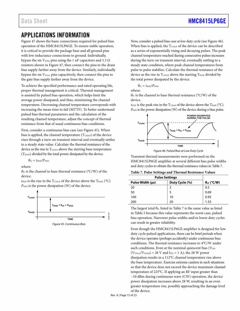
Now, consider a pulsed bias case at low duty cycle (see Figure 46). When bias is applied, the TCHAN of the device can be described as a series of exponentially rising and decaying pulses. The peak channel temperature reached during consecutive pulses increases during the turn-on transient interval, eventually settling to a steady state condition, where peak channel temperatures from pulse to pulse stabilize. Calculate the thermal resistance of the device as the rise in TCHAN above the starting TBASE divided by the total power dissipated by the device.
θJC = tRISE/PDISS where: θJC is the channel to base thermal resistance (°C/W) of the device. tRISE is the peak rise in the TCHAN of the device above the TBASE (°C). PDISS is the power dissipation (W) of the device during a bias pulse.
TRISE = θJC × PDISS
TCHAN
TBASE
POWER DISSIPATEDDURING THE PULSE
TIME 1668
8-04
6
Figure 46. Pulsed Bias at Low Duty Cycle
Transient thermal measurements were performed on the HMC8415LP6GE amplifier at several different bias pulse widths and duty cycles to obtain the thermal resistance values in Table 7.
Table 7. Pulse Settings and Thermal Resistance Values Pulse Settings
Pulse Width (µs) Duty Cycle (%) θJC (°C/W) 20 2 0.5 50 5 0.69 100 10 0.95 200 20 1.33
The largest total θJC listed in Table 7 is the same value as listed in Table 5 because this value represents the worst case, pulsed bias operation. Narrower pulse widths and/or lower duty cycles can result in greater reliability.
Even though the HMC8415LP6GE amplifier is designed for low duty cycle pulsed applications, there can be brief periods when the device operates (perhaps accidently) under continuous bias conditions. The thermal resistance increases to 4°C/W under such conditions. Even at the nominal quiescent bias (VDD (VDDxA/VDDxB) = 28 V and IDD = 1 A), the 28 W power dissipation results in a 112°C channel temperature rise above the base temperature. Exercise extreme caution in such situations so that the device does not exceed the device maximum channel temperature of 225°C. If applying an RF input greater than −10 dBm during continuous wave (CW) operation, the device power dissipation increases above 28 W, resulting in an even greater temperature rise, possibly approaching the damage level of the device.

HMC8415LP6GE Data Sheet
Rev. A | Page 16 of 23
Pulsed bias can be achieved in different ways. However, typical applications hold the gate bias constant, pulse the drain bias on (28 V) when amplification is required, and pulse the drain bias off (0 V) when the drain bias is no longer required. Drain bias pulsing typically requires implementation of a pulsor circuit that consists of heavy duty power components, such as power metal-oxide semiconductor field effect transistors (MOSFETs), MOSFET drivers, and power rectifiers. Large capacitors are also required because these capacitors serve as local reservoirs of charge, helping to provide the drain current demanded by the HMC8415LP6GE while maintaining a steady drain voltage during the on time of the pulse.
An example of such a pulsor is the Analog Devices, Inc., custom drain pulsor board shown in Figure 48. The pulsor board was developed specifically for this application and is included with the HMC8415LP6GE evaluation kit, EV1HMC8415LP6G. The HMC8415LP6GE characterization was performed on the
evaluation board, with VDD pulsing achieved through use of the pulsor board in combination with external dc voltage supplies for VDDxx and VGGxx and a pulse generator for triggering the VDD pulses. The dc connectors of both boards allow the boards to connect directly together without the need for extraneous flexible cabling. This rigid connection between the boards helps maintain a low inductance and low resistance connection, minimizing the occurrence of ringing and voltage drop. To help simplify the implementation of the HMC8415LP6GE with a drain bias pulsor circuit into customer applications, the complete drawing packages and bill of materials for both boards are available by submitting a Technical Support Request.
Before attempting to connect the EV1HMC8415LP6G to the pulsor board, closely review the schematics of both boards (see Figure 47 and Figure 48).

Data Sheet HMC8415LP6GE
Rev. A | Page 17 of 23
TYPICAL APPLICATION CIRCUIT AND PULSOR CIRCUIT Figure 47 shows the typical application circuit, and Figure 48 shows the drain bias typical pulsor circuit.
1
3
4
2
5
6
7
8
9
21
22
11
V GG
1B
12
V GG
2B
13
V GG
3B
14 15
V DD1
B
16
V DD2
B
17 18 19
V DD3
B
20
V DD3
B31
V DD3
A
23
24
25
26 J2RFOUT
GROUNDPADDLE
J1RFIN
27
28
29
30
10
32V D
D3A
333435
V DD2
A
36
V DD1
A
3738
V GG
3A
39
V GG
2A
40
V GG
1A
C7100pF
R270Ω
R40Ω+
+
+
C192.2nF
R260Ω
C311µF
R250Ω
C9100pF
R210Ω
R50Ω
C212.2nF
R200Ω
C331µF
R190Ω
C11100pF
R150Ω
R60Ω
C232.2nF
R140Ω
C351µF
R130Ω
C1100pF
R90Ω
R10Ω+
+
+
C132.2nF
R80Ω
C251µF
R70Ω
C3100pF
R330Ω
R20Ω
C152.2nF
R320Ω
C271µF
R310Ω
C5100pF
R390Ω
C21nF
R103.3Ω
C41nF
R343.3Ω
C61nF
R403.3Ω
C81nF
R283.3Ω
C101nF
R223.3Ω
C121nF
R163.3Ω
R30Ω
C172.2nF
R380Ω
C291µF
R370Ω
23 21 19 17 15 13 11 9 7 5 3 1J3
J4
24 22 20 18 16 14 12 10 8 6 4 2
2321191715131197531
24222018161412108642
1668
8-03
9
Figure 47. Typical Application Circuit

HMC8415LP6GE Data Sheet
Rev. A | Page 18 of 23
23 21 19 17 15 13 11 9 7 5 3 1J2
J3
24 22 20 18 16 14 12 10 8 6 4 2
2321191715131197531
24222018161412108642
J1
INPUTSFROM USER
30V DRAIN BIAS PULSER BOARDSIMPLIFIED SCHEMATIC
23
21
19
17
15
13
11
9
7
5
3
1
24
OPROBE
PULSE
GND
VG1
SENSE
VDD
OPROBE
CAPACITIVEBYPASSING
CAPACITIVEBYPASSING
POWERMOSFET
J4PULSED_VDDFOR MONITORING WITH HIGH-ZOSCILLOSCOPE PROBE
CONNECTSDIRECTLY TOEVAL BOARD J3
CONNECTSDIRECTLY TOEVAL BOARD J4
PULSED_VDD
PULSED_VDD
VG1
VG1
MOSFETDRIVER
GND
0Ω
GNDGND VBOOST
TANSIENTPROTECTION
PULSE INPUT SENSE+
GATE
SENSE–VDD
VG1
SENSE
VDD
2526
22
20
18
16
14
12
10
8
6
4
2
0Ω
1kΩ
1668
8-04
0
Figure 48. Typical Pulsor Circuit

Data Sheet HMC8415LP6GE
Rev. A | Page 19 of 23
USING THE EV1HMC8415LP6G WITH THE DRAIN BIAS PULSOR BOARD The following description assumes that pulsed measurements were made and that a current probe was used to measure IDD. When neither is possible with the equipment available, approximations must be made as described in the Making Average to Pulsed Approximations section.
The connections required for using the EV1HMC8415LP6G with the drain bias pulsor board are shown in Figure 49. Before applying any bias or signals, the pulsor board must interconnect with the EV1HMC8415LP6G so that the pulsor board (J2) mates with the EV1HMC8415LP6G (J3) and the pulsor board (J3) mates with the EV1HMC8415LP6G (J4). The
only externally wired connections needed are to the J1 connector of the pulsor board: VDD, SENSE (from the +S VDD supply), VG1, PULSE, and all signal GNDs, including the –S VDD supply. VG1 passes from the Pulsor J1-VG1 directly through the pulsor board to the gate pins of the evaluation board. For the Pulsor J1-VDD and its GND connections, the use of heavy gauge twister pair wires is recommended to minimize voltage drop. The J4 coaxial connector of the pulsor board allows the convenient monitoring of the VDD_PULSE signal by using an oscilloscope.
PULSE GENERATOR
SYNC OUT PULSE OUT
DRAIN PULSERBOARD
HMC8415 EVAL BOARD
J2J3
RFOUTRFINATTENUATOR
INPUT OUTPUT
POWER METER
TRIGGER IN CH 1 CH 2
DIRECTIONALCOUPLER
INPUTCOUPLED
OUTPUT
DIRECTIONALCOUPLER
INPUTCOUPLED
OUTPUT
RF SIGNALGENERATOR
TRIGGER IN RF OUT
AMPLIFIEROUTPUTINPUT
ATTENUATORPOWER
SENSOR 1OUTPUTINPUT
50ΩTERMINATIONINPUT
AMPLIFIEROUTPUT INPUT
OSCILLOSCOPECH 1 CH 3CH 2
VDD AND IDDMONITORING
TRIGGER
TEKTRONIXTCPA300
CURRENTPROBE
TEKTRONIXTCPA312A
DC SUPPLY
VDD
–S +S–V +V
DC SUPPLY
VGG
–S +S–V +V
J4VDD_PULSE
VDD VG1 GNDSENSE PULSE
J3
J1
J4
ATTENUATORPOWER
SENSOR 2OUTPUTINPUT
16688-041
Figure 49. Setup Block Diagram

HMC8415LP6GE Data Sheet
Rev. A | Page 20 of 23
RECOMMENDED BIAS SEQUENCE Power-Up Bias Concept for the EV1HMC8415LP6G with the Pulsor
A proper set of dc bias conditions always requires that the gate be biased to a voltage that does not result in excessive drain current, regardless of whether the drain bias is constant or pulsed. For this reason, always apply a gate bias voltage to Pulsor J1-VG1 prior to the application of a voltage to Pulsor J1-VDD. VG1 = −6 V is considered a safe starting value. With a pulsed logic signal applied to Pulsor J1-PULSE and 28 V applied to Pulsor J1-VDD, a pulsed voltage between 0 V (for PULSE = logic low) and VDD = 28 V (for PULSE = logic high) becomes available at Pulsor J2-VDD_PULSE and Pulsor J3-VDD_PULSE and, therefore, at the drains of the device under test (DUT). When the gate bias voltage (applied to Pulsor J1-VG1) is available at the gates simultaneously with VDD_PULSE at the
drains, a drain current proportional to VG1 flows. VG1 can be adjusted until the target pulsed IDQ is achieved. With this pulsor board, J1-VDD has a 35 V maximum above which damage can occur to the pulsor.
The J1-PULSE and VDD_PULSE pulse width and duty cycle limits for reliable operation are as follows:
Pulse width = 500 μs maximum Duty cycle = 20% maximum
Power-Down Bias Concept for the EV1HMC8415LP6G with the Pulsor
The power-down bias sequence follows from the power-up bias sequence. Bring Pulsor J1-PULSE to logic low to remove VDD_PULSE, and then power down Pulsor J1-VDD followed by powering down Pulsor J1-VG1.

Data Sheet HMC8415LP6GE
Rev. A | Page 21 of 23
MAKING AVERAGE TO PULSED APPROXIMATIONS To measure RF power, IDD, and PAE accurately in a pulsed manner, use instruments offering pulse triggered measurements. When pulse triggered instruments are not available but simpler instruments with adequate averaging capabilities are, approximations can be made with the understanding that the approximations can result in lower accuracy of measurement. The most common approximations involve measuring the average values of parameters and then adjusting those values to account for the duty cycle of operation. Approximating in this manner can result in errors due to the limited measurement bandwidths of the instruments and/or the inclusion of on/off transients and/or partial periods in the measurement. So that partial periods do not contribute significant errors to the measurements, perform the averaging over a large number of pulse periods. The results of such approximations can vary with the instruments and settings used. Therefore, experimentation can be necessary to achieve credible and repeatable results. When it is not possible to make pulse triggered measurements, the only pulse connection required is the one from the pulse generator to the J1 connector of the pulsor (see Figure 49).
Depending on the implementation of the HMC8415LP6GE and the pulsor into customer applications, adjustments of the pulse circuit may be desired if the on and off transitions are accompanied by excessive drain supply ringing. Synchronous with the drain pulses, the VGGxx bias and RFIN signal can also be pulsed.
Unless otherwise noted, all measurement data shown within this data sheet was taken using the typical application circuit (see Figure 47) as implemented on the evaluation board (see Figure 50), with the drain bias pulsed at 28 V by the pulsor board (see Figure 48) to achieve the nominal IDQ of 1000 mA at a pulse width of 100 µs, and 10% duty cycle. Operating at different drain voltages or different drain quiescent currents affects performance, as shown in the Typical Performance Characteristics section. For applications having lower power and gain requirements, operation at lower VDDxx and IDQ can help reduce power consumption. Due to thermal considerations, the use of lower duty cycles and shorter pulse widths can sometimes result in improved power and PAE.

HMC8415LP6GE Data Sheet
Rev. A | Page 22 of 23
EVALUATION PCB The EV1HMC8415LP6G (600-01639-00-2) evaluation PCB is shown in Figure 50.
BILL OF MATERIALS Use RF circuit design techniques for the circuit board used in the application. Provide 50 Ω impedance for the signal lines and directly connect the package ground leads and exposed pad to the ground plane, similar to that shown in Figure 50. Use a sufficient number of via holes to connect the top and bottom ground planes. The evaluation PCB shown in Figure 50 is available from Analog Devices upon request.
1668
8-04
2
Figure 50. Evaluation PCB
Table 8. Bill of Materials for the Evaluation PCB EV1HMC8415LP6G (600-01639-00-2) Item Description J1, J2 SMA connectors J3, J4 DC pins R1 to R9, R13 to R15, R19 to R21, R25 to R27, R31 to
R33, R37 to R39 0 Ω resistors, 0402 package
C2, C4, C6, C8, C10, C12 1000 pF capacitors, 0402 package C1, C3, C5, C7, C9, C11 100 pF capacitors, 0402 package C13, C15, C17, C19, C21, C23 2200 pF capacitors, 0603 package C25, C27, C29, C31, C33, C35 1 µF capacitors, 0603 package U1 HMC8415LP6GE PCB 600-01639-00-2 evaluation PCB; circuit board material: Rogers 4350 or Arlon 25FR

Data Sheet HMC8415LP6GE
Rev. A | Page 23 of 23
OUTLINE DIMENSIONS
10-0
8-20
18-A
0.50BSC
BOTTOM VIEWTOP VIEW
0.05 MAX0.02 NOM
0.203 REF
COPLANARITY0.08
0.300.250.18
6.106.00 SQ5.90
0.800.750.70
FOR PROPER CONNECTION OFTHE EXPOSED PAD, REFER TOTHE PIN CONFIGURATION ANDFUNCTION DESCRIPTIONSSECTION OF THIS DATA SHEET.
0.450.400.35
0.20 MIN
4.704.60 SQ4.50
COMPLIANT TO JEDEC STANDARDS MO-220-WJJD-5
401
1110
2021
3031
END VIEW
EXPOSEDPAD
PKG
-005
131
P IN 1IN D ICATO R AR E A OP TIO N S(SEE DETAIL A)
DETAIL A(JEDEC 95)
SEATINGPLANE
PIN 1INDICATOR
AREA
Figure 51. 40-Lead Lead Frame Chip Scale Package [LFCSP]
6 mm × 6 mm Body and 0.75 mm Package Height (CP-40-7)
Dimensions shown in millimeters
ORDERING GUIDE Model1 Temperature Range MSL Rating2 Package Description3 Package Option HMC8415LP6GE −40°C to +85°C 3 40-Lead Lead Frame Chip Scale Package [LFCSP] CP-40-7 HMC8415LP6GETR −40°C to +85°C 3 40-Lead Lead Frame Chip Scale Package [LFCSP] CP-40-7 EV1HMC8415LP6G Evaluation Board 1 The HMC8415LP6GE and HMC8415LP6GETR are RoHS compliant parts. 2 See the Absolute Maximum Ratings section for additional information. 3 The HMC8415LP6GE and the HMC8415LP6GETR are low stress injection molded plastic and their lead finish is 100% matte Sn.
©2018–2019 Analog Devices, Inc. All rights reserved. Trademarks and registered trademarks are the property of their respective owners. D16688-0-4/19(A)