3D X-Ray Microscopy: A Non Destructive High … X-Ray Microscopy: A Non Destructive High Resolution...
8
3D X-Ray Microscopy: A Non Destructive High Resolution Imaging Technology That Replaces Physical Cross-Sectioning For 3DIC Packaging Yuri Sylvester, Bruce Johnson, Raleigh Estrada, Luke Hunter, Kevin Fahey Xradia, Inc.* 4385 Hopyard Rd. Suite 100 Pleasanton, CA 94588, U.S.A Tulip Chou, Y.L. Kuo Product Failure Analysis Department (PFA) Taiwan Semiconductor Manufacturing Company, Ltd. No. 9, Creation Rd I, Science-Based Industrial Park, Hsinchu, Taiwan [email protected] resolution and high contrast) side-view images give enough detail to measure critical structures and defects. Despite these advantages, physical cross-sectioning is far from an optimal solution to address the increasing requirements of 3DIC packages because it is destructive and time consuming. Also, stress relief produced by cross-sectioning may in fact obfuscate clues—by introducing debris or damaging soft layers—about the original root cause of the defect of interest. Furthermore, defects can be completely missed if the incorrect polishing orientation is chosen. XRM, a powerful 3D X-Ray variant technique, has demonstrated success in replacing physical cross-sections in FA labs and shows great potential to bridge the gaps in 3DIC production metrology [1]-[2]. Unlike 2D X-Ray and conventional MicroCT techniques that rely exclusively in geometric magnification with low signal-to- noise flat panel detectors, XRM employs geometric and optical image magnification to achieve higher spatial resolution, even for large package sizes. In this way XRM is being used to collect high-quality non-destructive images that are comparable in quality to the ones obtained from Scanning Electron Microscope (SEM) and optical micrographs, enabling an unparalleled imaging capability to the FA and process development workflows (see Fig 1) [3]. Fig. 1. Proposed use of non-destructive X-Ray Microscopy (XRM) to improve the units per hour (UPH) of intact samples requiring inspection in the Failure Analysis Workflow and to shorten the time-to-market of 3DIC process development [3]. The traditional non-destructive techniques found in most FA labs today are becoming unsuitable to address the increasingly complex multilayered architectures of 3DIC packages. X-Ray Radiography (which includes “2D X-Ray” and “3D X-Ray MicroCT”) and Scanning Acoustic Abstract—In this paper, we describe the novel technique of using leading edge X-Ray Microscopy (XRM) technology to replace physical cross-sectioning in Failure Analysis (FA) and 3- Dimensional Integrated Circuit (3DIC) process development. Contrary to general consensus that 3D X-Ray is too slow, we explain how XRM can be used to obtain high quality cross-section images within 5-300min per measurement depending on the physical properties (materials, feature sizes, and outer dimensions) of the sample and the minimum tolerable image quality needed to visualize a defect. The specifics of the inspection technique itself and how X-rays interact with the sample to achieve high-quality images will be discussed and contrasted with conventional 3D MicroCT technology. Furthermore, understanding the effects that imaging parameters, such as voltage, power, exposure time, resolution, number of projections, etc, have in the quality of an image, can help the user reduce the 3D X-Ray inspection time considerably. A TSMC test vehicle package is used to illustrate the effects of inspection time in image quality, and to compare and contrast the quality of an optical image taken from a physical cross-section and a virtual cross-section image taken from an XRM tomography. Keywords—3D X-Ray Microscopy, TSV, 3DIC, metrology, non- destructive inspection, Failure Analysis, Computed Tomography, underfill, cracks, voids, non-contact open, interposer I. INTRODUCTION 2D X-Ray and conventional Micro Computed Tomography (MicroCT) technologies used in the development of ball grid array, thermal compression bonding, and flip chip technologies cannot be extended to provide the image quality needed for the development of 3DIC packages. While the resolution provided by these techniques is useful to image large voids, rough misalignments, and non-contact opens from top-views of first- and second-level interconnects, conventional X-Ray techniques quickly become inadequate as more layers with smaller feature sizes are stacked on top of each other as it is in the case of multi-chip packages, interposers, and through-silicon vias [1]. Physical cross- sectioning is still the most widely used technique for 3DIC package development because the high quality (high As published in the Proceedings of the 24th Annual IEEE/SEMI Advanced Semiconductors Manufacturing Conference (ASMC 2013) May 14-16, 2013, Saratoga Springs, New York. *Xradia was acquired by Carl Zeiss in 2013. 1
Transcript of 3D X-Ray Microscopy: A Non Destructive High … X-Ray Microscopy: A Non Destructive High Resolution...
3D X-Ray Microscopy: A Non Destructive High Resolution Imaging Technology That Replaces Physical Cross-Sectioning For 3DIC Packaging
Yuri Sylvester, Bruce Johnson, Raleigh Estrada, Luke Hunter,
Kevin Fahey Xradia, Inc.*
4385 Hopyard Rd. Suite 100 Pleasanton, CA 94588, U.S.A
Tulip Chou, Y.L. Kuo Product Failure Analysis Department (PFA)
Taiwan Semiconductor Manufacturing Company, Ltd. No. 9, Creation Rd I, Science-Based Industrial Park,
Hsinchu, Taiwan [email protected]
resolution and high contrast) side-view images give enough detail to measure critical structures and defects. Despite these advantages, physical cross-sectioning is far from an optimal solution to address the increasing requirements of 3DIC packages because it is destructive and time consuming. Also, stress relief produced by cross-sectioning may in fact obfuscate clues—by introducing debris or damaging soft layers—about the original root cause of the defect of interest. Furthermore, defects can be completely missed if the incorrect polishing orientation is chosen. XRM, a powerful 3D X-Ray variant technique, has demonstrated success in replacing physical cross-sections in FA labs and shows great potential to bridge the gaps in 3DIC production metrology [1]-[2]. Unlike 2D X-Ray and conventional MicroCT techniques that rely exclusively in geometric magnification with low signal-to-noise flat panel detectors, XRM employs geometric and optical image magnification to achieve higher spatial resolution, even for large package sizes. In this way XRM is being used to collect high-quality non-destructive images that are comparable in quality to the ones obtained from Scanning Electron Microscope (SEM) and optical micrographs, enabling an unparalleled imaging capability to the FA and process development workflows (see Fig 1) [3].
Fig. 1. Proposed use of non-destructive X-Ray Microscopy (XRM) to improve the units per hour (UPH) of intact samples requiring inspection in the Failure Analysis Workflow and to shorten the time-to-market of 3DIC process development [3]. The traditional non-destructive techniques found in most FA labs today are becoming unsuitable to address the increasingly complex multilayered architectures of 3DIC packages. X-Ray Radiography (which includes “2D X-Ray” and “3D X-Ray MicroCT”) and Scanning Acoustic
Abstract—In this paper, we describe the novel technique of using leading edge X-Ray Microscopy (XRM) technology to replace physical cross-sectioning in Failure Analysis (FA) and 3-Dimensional Integrated Circuit (3DIC) process development. Contrary to general consensus that 3D X-Ray is too slow, we explain how XRM can be used to obtain high quality cross-section images within 5-300min per measurement depending on the physical properties (materials, feature sizes, and outer dimensions) of the sample and the minimum tolerable image quality needed to visualize a defect. The specifics of the inspection technique itself and how X-rays interact with the sample to achieve high-quality images will be discussed and contrasted with conventional 3D MicroCT technology. Furthermore, understanding the effects that imaging parameters, such as voltage, power, exposure time, resolution, number of projections, etc, have in the quality of an image, can help the user reduce the 3D X-Ray inspection time considerably. A TSMC test vehicle package is used to illustrate the effects of inspection time in image quality, and to compare and contrast the quality of an optical image taken from a physical cross-section and a virtual cross-section image taken from an XRM tomography.
Keywords—3D X-Ray Microscopy, TSV, 3DIC, metrology, non-destructive inspection, Failure Analysis, Computed Tomography, underfill, cracks, voids, non-contact open, interposer
I. INTRODUCTION
2D X-Ray and conventional Micro Computed Tomography (MicroCT) technologies used in the development of ball grid array, thermal compression bonding, and flip chip technologies cannot be extended to provide the image quality needed for the development of 3DIC packages. While the resolution provided by these techniques is useful to image large voids, rough misalignments, and non-contact opens from top-views of first- and second-level interconnects, conventional X-Ray techniques quickly become inadequate as more layers with smaller feature sizes are stacked on top of each other as it is in the case of multi-chip packages, interposers, and through-silicon vias [1]. Physical cross-sectioning is still the most widely used technique for 3DIC package development because the high quality (high
As published in the Proceedings of the 24th Annual IEEE/SEMI Advanced Semiconductors Manufacturing Conference (ASMC 2013)May 14-16, 2013, Saratoga Springs, New York. *Xradia was acquired by Carl Zeiss in 2013.
1
Microscopy techniques have been the standard non-destructive techniques for locating and identifying failure causes. However, the resolution that they deliver is no longer able to meet the requirements of advanced packages, forcing users to resort to destructive techniques.
Recent advances in XRM obtain near-SEM quality images with reasonable data collection times. TO appreciate the capabilities and limitations of this novel technique as it applies to 3DIC packaging, it is important to understand the differences between MicroCT and XRM techniques and the way X-rays interact with the sample in XRM to achieve high quality images.
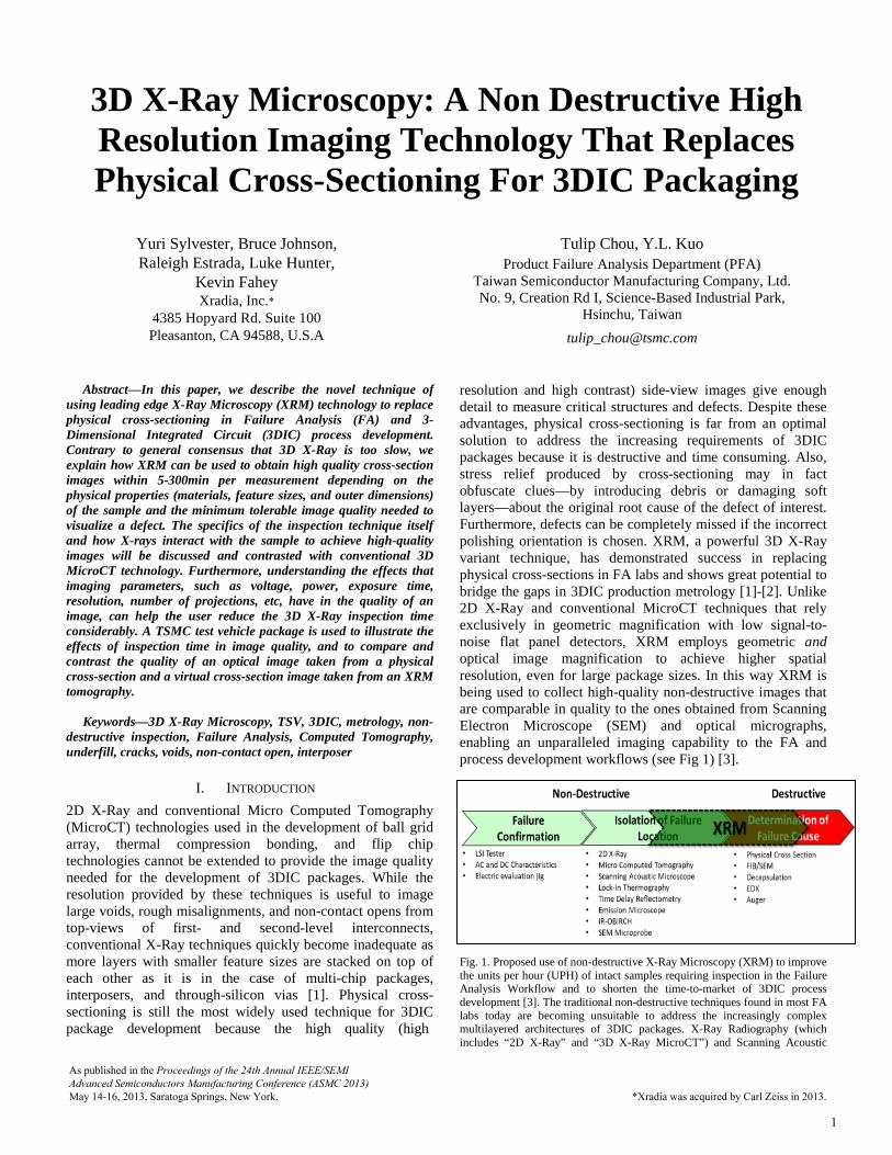
II. MICROCT VS. XRM3D X-Ray data is a virtual volumetric region in space that is reconstructed from many 2D X-Ray projections passing through a sample as it rotates about an axis. The two most known 3D data collection techniques to the semiconductor industry are Laminography and Computed Tomography (CT). Despite being fast, Laminography has physical limitations—2D projections are collected at higher incident angles, causing image artifacts—that fundamentally limit its ability to achieve high spatial resolution. CT, on the other hand, uses a filtered-back projection reconstruction technique to generate 3D virtual models of internal structures from 2D X-ray projections that are collected in small intervals over a range of angles, typically 180° or 360°. MicroCT was developed to achieve micrometer voxel (the 3D analog of a 2D pixel) resolution. However, this technique is subject to tradeoffs between sample size and achievable spatial resolution. The relationship can be modeled by (1),
(1)
where dtotal is the total spatial resolution, rD is detector pixel size, S is X-ray spot size, M is geometric magnification, rso is source-to-object distance, and rod is object-to-detector distance, respectively and graphically represented in Fig 2 [2].
Furthermore, to maximize spatial resolution, MicroCT relies on maximizing geometric magnification, M, which is described by (2) below.
(2)
Thus, in order to maximize geometric magnification, the source-to-object distance must be made very small, limiting the working distance available for high-resolution analysis. As a result, high-resolution imaging of larger samples is not possible. To improve on this limitation, MicroCT can continue to develop in three main ways:
a) Increase the equipment footprint: This increasesthe sample-to-detector distance, thus achieving higher geometric magnification for larger samples. However, the impact of this leads to not only a larger equipment, but also degrades the image quality because having the source and detector so far apart reduces the signal-to-noise ratio of the image.
b) Reduce the source spot size: The X-ray beam isgenerated by focusing an electron beam onto a target material (typically Tungsten or Diamond). In order to achieve a small spot size, high densities of energy need to be focused onto a very small region, where heat dissipation becomes an important challenge that can cause short filament lifetimes and/or unstable X-ray power output. Commercially available sources with spot sizes down to ~0.25µm are available, but they are limited to low power levels (2-5W) only and thus lower energies (up to ~90kV). At this energy range (0-90kV) the effective penetration of highly attenuating materials (as it is typical in materials found in 3DIC packages, like SAC305 solders, Cu, Au, fiber glass, etc.) is minimal, making these sources unsuitable for a wide range of semiconductor samples. In contrast, XRM does not rely on small source spot sizes to achieve high resolution, since magnification is mostly achieved by optical means as opposed to geometric means. For his reason, higher power sources can be used in these systems, allowing for higher voltages that can penetrate
Mrr
Srd so
odD
total
22
+
=
so
odso
rrrM +
=
Fig. 2. The red region shows the tradeoff between resolution and sample size in conventional MicroCT. The green line shows “resolution-at-distance” achievable with XRM enhanced optics. The image on the right illustrates how geometric magnification is decreased in a full-angle CT scan as the sample size increases.
2
through denser materials. A typical X-ray source used in XRM equipment can achieve stable 10W output at 150kV with spot sizes of 1-3µm and achieve higher spatial resolution than MicroCT with a source spot size of 0.25µm.
c) Reduce the pixel size of flat panel detectors:Current detector technologies being used in X-ray systems include flat panel detectors and charge-coupled detectors (CCD). Flat panel detectors are able to obtain larger fields of view (FOV) at the expense of lower signal and larger pixel sizes (typically 200-300µm) whereas CCDs offer smaller FOVs at a gain in quantum efficiency and pixel size (typically ~35µm). Increasing the size of a flat panel detector (e.g. going from a 4Mp to a 16Mp) only increases the FOV and digital magnification, not spatial resolution. Digital magnification does not lead to better image detail; it only gives the ability to zoom-in further in the display screen.
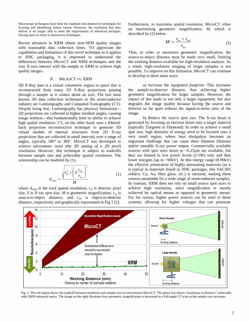
XRM takes advantage of state-of-the-art detectors (optics with enhanced scintillators) developed for synchrotron facilities to achieve high spatial resolution. Spatial resolution of an image is not only achieved by having high pixel resolution, but also by having high contrast and a high signal-to-noise ratio, so as to be able to distinguish between two neighboring features, in space, with high fidelity. In XRM, the physical and crystallographic properties of state-of-the-art scintillators are tuned for objectives of varying magnifications, allowing the useful part of the target energy spectrum to be converted into visible light with higher quantum efficiencies than in conventional flat panel detectors. These photons are then further magnified in the objectives, which are subsequently registered with a CCD. It is precisely this feature—optical magnification with enhanced spectral properties—which allows XRM to achieve high spatial resolution and high contrast even at large working distances (see Fig 3).
A. Effects of imaging parameters to image quality and scantimes
All CT reconstructed scans are subject to various imaging artifacts that can affect overall image quality. Generally speaking, 3DIC packages require better image quality (higher spatial resolution and higher contrast) than its 2DIC counterparts, so understanding artifacts and their reduction techniques is essential to achieve SEM-like images non-
destructively. Although not discussed here, among the most common types of CT artifacts affecting semiconductor samples are beam hardening, under sampling, and photon starvation [4]. Likewise, understanding the effects that imaging parameters have on the reconstructed data can help understand the capabilities and limitations of XRM as it applies to replacing physical cross-sections in specific applications in 3DIC packages and as the technology evolves to address gaps in in-line metrology.
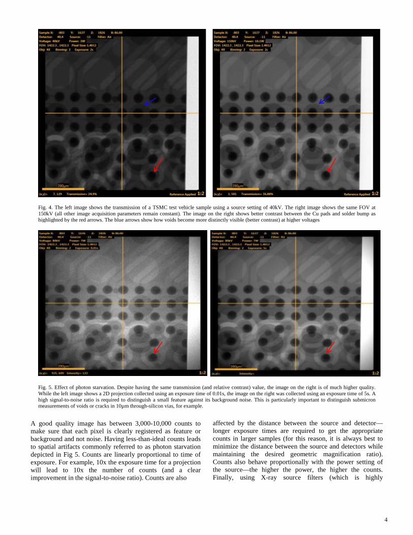
a) Energy (kV): The energy of the source determines theextent to which the X-rays penetrate through the sample, which in turn determines the percent absorption and percent transmission through the sample. If a sample is highly attenuating—composed of high-atomic number (Z) materials or if it is thick—then higher energy X-rays are needed to penetrate through the sample and obtain acceptable values of transmission. During reconstruction, a grey scale value is assigned to each voxel based on the percent transmission of X-rays passing through each voxel at each angle of projection in the tomography. These grey scale values determine the relative contrast that distinct features and/or materials will display in the virtual cross-section image. An ideal tomography has transmission values between 25% and 35% through all the angle projections through the feature of interest. For example, low energy is required to generate absorption contrast between air bubbles and low-attenuating underfill layers. If high energies are used instead, the transmission through the underfill layer would be too high (<90%), creating very little contrast in the air bubbles. Alternatively, high energy is needed to generate contrast between voids and solder in solder bumps (see Fig 4). If low energies are used, the transmission will be too low and little signal will go through the sample. Filters that absorb the lower energies from the x-ray spectrum are commonly used to boost
the transmission through high-attenuating materials by making the average energy of the X-ray beam higher. Filters are also used in the same way to reduce beam hardening artifacts [4].
b) Signal-to-noise ratio:After the X-rays are convertedinto photons by the scintillator, they are condensed by the objectives and registered in the CCD. The number of photons that hit each pixel of the scintillator is referred to as counts.
Fig. 3. XRM does not depend on geometric magnification to achieve high spatial resolution.
3
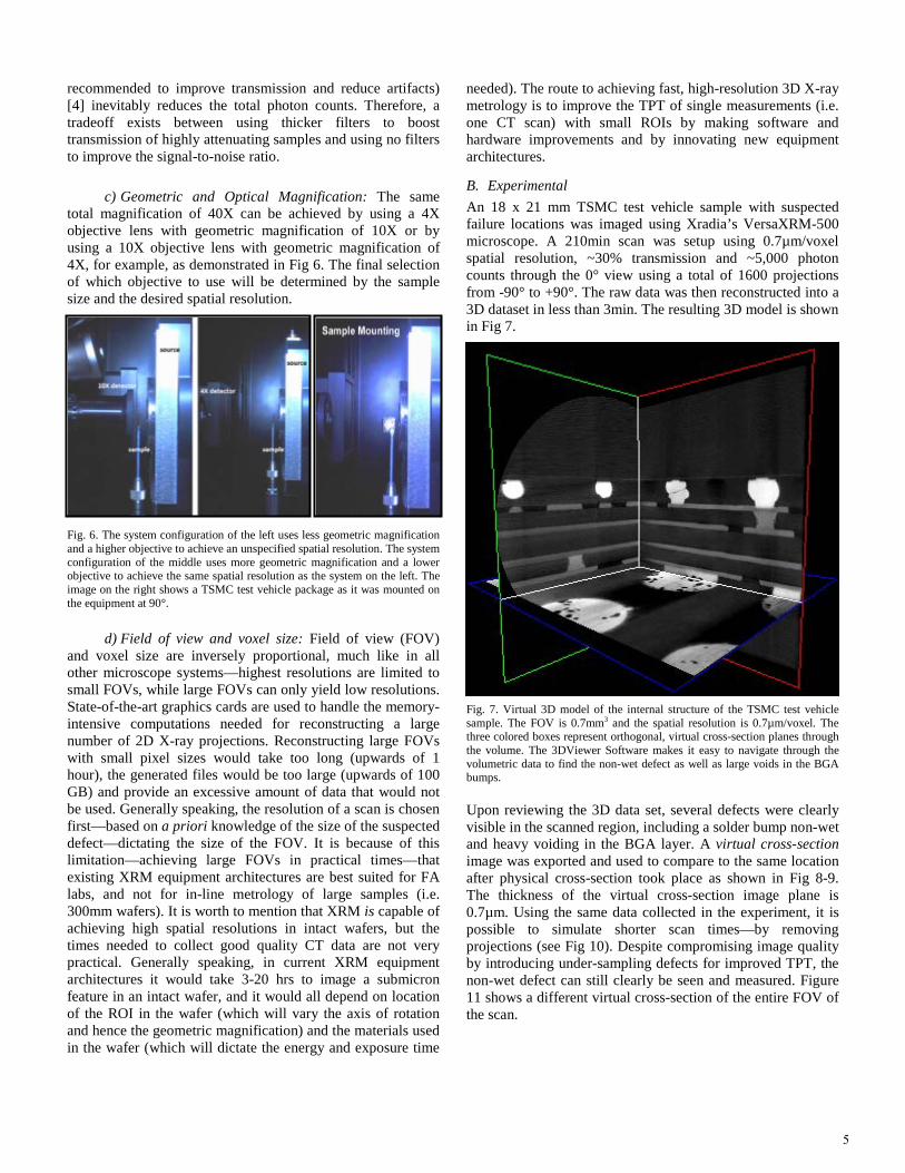
A good quality image has between 3,000-10,000 counts to make sure that each pixel is clearly registered as feature or background and not noise. Having less-than-ideal counts leads to spatial artifacts commonly referred to as photon starvation depicted in Fig 5. Counts are linearly proportional to time of exposure. For example, 10x the exposure time for a projection will lead to 10x the number of counts (and a clear improvement in the signal-to-noise ratio). Counts are also
affected by the distance between the source and detector—longer exposure times are required to get the appropriate counts in larger samples (for this reason, it is always best to minimize the distance between the source and detectors while maintaining the desired geometric magnification ratio). Counts also behave proportionally with the power setting of the source—the higher the power, the higher the counts. Finally, using X-ray source filters (which is highly
Fig. 4. The left image shows the transmission of a TSMC test vehicle sample using a source setting of 40kV. The right image shows the same FOV at 150kV (all other image acquisition parameters remain constant). The image on the right shows better contrast between the Cu pads and solder bump as highlighted by the red arrows. The blue arrows show how voids become more distinctly visible (better contrast) at higher voltages
Fig. 5. Effect of photon starvation. Despite having the same transmission (and relative contrast) value, the image on the right is of much higher quality. While the left image shows a 2D projection collected using an exposure time of 0.01s, the image on the right was collected using an exposure time of 5s. A high signal-to-noise ratio is required to distinguish a small feature against its background noise. This is particularly important to distinguish submicron measurements of voids or cracks in 10µm through-silicon vias, for example.
4
recommended to improve transmission and reduce artifacts) [4] inevitably reduces the total photon counts. Therefore, atradeoff exists between using thicker filters to boosttransmission of highly attenuating samples and using no filtersto improve the signal-to-noise ratio.
c) Geometric and Optical Magnification: The sametotal magnification of 40X can be achieved by using a 4X objective lens with geometric magnification of 10X or by using a 10X objective lens with geometric magnification of 4X, for example, as demonstrated in Fig 6. The final selection of which objective to use will be determined by the sample size and the desired spatial resolution.
Fig. 6. The system configuration of the left uses less geometric magnification and a higher objective to achieve an unspecified spatial resolution. The system configuration of the middle uses more geometric magnification and a lower objective to achieve the same spatial resolution as the system on the left. The image on the right shows a TSMC test vehicle package as it was mounted on the equipment at 90°.
d) Field of view and voxel size: Field of view (FOV)and voxel size are inversely proportional, much like in all other microscope systems—highest resolutions are limited to small FOVs, while large FOVs can only yield low resolutions. State-of-the-art graphics cards are used to handle the memory-intensive computations needed for reconstructing a large number of 2D X-ray projections. Reconstructing large FOVs with small pixel sizes would take too long (upwards of 1 hour), the generated files would be too large (upwards of 100 GB) and provide an excessive amount of data that would not be used. Generally speaking, the resolution of a scan is chosen first—based on a priori knowledge of the size of the suspected defect—dictating the size of the FOV. It is because of this limitation—achieving large FOVs in practical times—that existing XRM equipment architectures are best suited for FA labs, and not for in-line metrology of large samples (i.e. 300mm wafers). It is worth to mention that XRM is capable of achieving high spatial resolutions in intact wafers, but the times needed to collect good quality CT data are not very practical. Generally speaking, in current XRM equipment architectures it would take 3-20 hrs to image a submicron feature in an intact wafer, and it would all depend on location of the ROI in the wafer (which will vary the axis of rotation and hence the geometric magnification) and the materials used in the wafer (which will dictate the energy and exposure time
needed). The route to achieving fast, high-resolution 3D X-ray metrology is to improve the TPT of single measurements (i.e. one CT scan) with small ROIs by making software and hardware improvements and by innovating new equipment architectures.
B. ExperimentalAn 18 x 21 mm TSMC test vehicle sample with suspected failure locations was imaged using Xradia’s VersaXRM-500 microscope. A 210min scan was setup using 0.7µm/voxel spatial resolution, ~30% transmission and ~5,000 photon counts through the 0° view using a total of 1600 projections from -90° to +90°. The raw data was then reconstructed into a 3D dataset in less than 3min. The resulting 3D model is shown in Fig 7.
Fig. 7. Virtual 3D model of the internal structure of the TSMC test vehicle sample. The FOV is 0.7mm3 and the spatial resolution is 0.7µm/voxel. The three colored boxes represent orthogonal, virtual cross-section planes through the volume. The 3DViewer Software makes it easy to navigate through the volumetric data to find the non-wet defect as well as large voids in the BGA bumps.
Upon reviewing the 3D data set, several defects were clearly visible in the scanned region, including a solder bump non-wet and heavy voiding in the BGA layer. A virtual cross-section image was exported and used to compare to the same location after physical cross-section took place as shown in Fig 8-9. The thickness of the virtual cross-section image plane is 0.7µm. Using the same data collected in the experiment, it is possible to simulate shorter scan times—by removing projections (see Fig 10). Despite compromising image quality by introducing under-sampling defects for improved TPT, the non-wet defect can still clearly be seen and measured. Figure 11 shows a different virtual cross-section of the entire FOV of the scan.
5
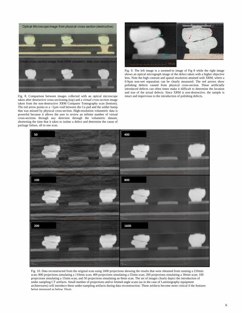
Fig. 8. Comparison between images collected with an optical microscope taken after destructive cross-sectioning (top) and a virtual cross-section image taken from the non-destructive XRM Computer Tomography scan (bottom). The red arrow points to a ~2µm void between the Cu pad and the solder bump that was missed by physical cross-section. High-resolution volumetric data is powerful because it allows the user to review an infinite number of virtual cross-sections through any direction through the volumetric dataset, shortening the time that it takes to isolate a defect and determine the cause of package failure, all in one scan.
Fig. 9. The left image is a zoomed-in image of Fig 8 while the right image shows an optical micrograph image of the defect taken with a higher objective lens. Note the high contrast and spatial resolution attained with XRM, where a 0.9µm non-wet separation can be clearly measured. The red arrows show polishing defects caused from physical cross-section. These artificially introduced defects can often times make it difficult to determine the location and size of the actual defects. Since XRM is non-destructive, the sample is intact and impervious to the introduction of polishing defects.
50 400
100 800
200 1600
Fig. 10. Data reconstructed from the original scan using 1600 projections showing the results that were obtained from running a 210min scan; 800 projections simulating a 110min scan; 400 projections simulating a 55min scan; 200 projections simulating a 30min scan; 100 projections simulating a 15min scan; and 50 projections simulating an 8min scan. The set of images clearly depict the introduction of under sampling CT artifacts. Small number of projections and/or limited angle scans (as in the case of Laminography equipment architectures) will introduce these under-sampling artifacts during data reconstruction. These artifacts become more critical if the features being measured as below 10µm.
6
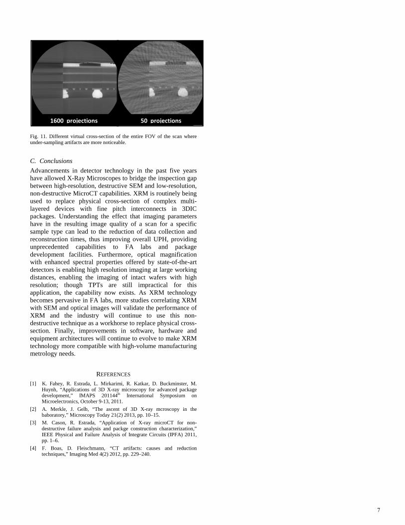
Fig. 11. Different virtual cross-section of the entire FOV of the scan where under-sampling artifacts are more noticeable.
C. ConclusionsAdvancements in detector technology in the past five years have allowed X-Ray Microscopes to bridge the inspection gap between high-resolution, destructive SEM and low-resolution, non-destructive MicroCT capabilities. XRM is routinely being used to replace physical cross-section of complex multi-layered devices with fine pitch interconnects in 3DIC packages. Understanding the effect that imaging parameters have in the resulting image quality of a scan for a specific sample type can lead to the reduction of data collection and reconstruction times, thus improving overall UPH, providing unprecedented capabilities to FA labs and package development facilities. Furthermore, optical magnification with enhanced spectral properties offered by state-of-the-art detectors is enabling high resolution imaging at large working distances, enabling the imaging of intact wafers with high resolution; though TPTs are still impractical for this application, the capability now exists. As XRM technology becomes pervasive in FA labs, more studies correlating XRM with SEM and optical images will validate the performance of XRM and the industry will continue to use this non-destructive technique as a workhorse to replace physical cross-section. Finally, improvements in software, hardware and equipment architectures will continue to evolve to make XRM technology more compatible with high-volume manufacturing metrology needs.
REFERENCES [1] K. Fahey, R. Estrada, L. Mirkarimi, R. Katkar, D. Buckminster, M.
Huynh, “Applications of 3D X-ray microscopy for advanced packagedevelopment,” IMAPS 201144th International Symposium onMicroelectronics, October 9-13, 2011.
[2] A. Merkle, J. Gelb, “The ascent of 3D X-ray mcroscopy in thebaboratory,” Microscopy Today 21(2) 2013, pp. 10–15.
[3] M. Cason, R. Estrada, “Application of X-ray microCT for non-destructive failure analysis and packge construction characterization,”IEEE Physical and Failure Analysis of Integrate Circuits (IPFA) 2011,pp. 1–6.
[4] F. Boas, D. Fleischmann, “CT artifacts: causes and reductiontechniques,” Imaging Med 4(2) 2012, pp. 229–240.
50 projections 1600 projections
7

Carl ZEISS SMT PCS Group4385 Hopyard RoadPleasanton, CA 94588 USA www.zeiss.com/pcs
Repr
inte
d by
Car
l Zei
ss S
MT
with
per
mis
sion
per
mis
sion
fro
m S
EMI.