3526 IEEE JOURNAL OF SOLID-STATE CIRCUITS, …spalermo/ecen689/dfe_iir_highz_rx_kim...3526 IEEE...
13
3526 IEEE JOURNAL OF SOLID-STATE CIRCUITS, VOL. 44, NO. 12, DECEMBER 2009 A 10-Gb/s Compact Low-Power Serial I/O With DFE-IIR Equalization in 65-nm CMOS Byungsub Kim, Student Member, IEEE, Yong Liu, Member, IEEE, Timothy O. Dickson, Member, IEEE, John F. Bulzacchelli, Member, IEEE, and Daniel J. Friedman, Member, IEEE Abstract—A compact and power-efficient serial I/O targeting dense silicon carrier interconnects is reported. Based on expected channel characteristics, the proposed I/O features low-impedance transmitter termination, high-impedance receiver termination, and a receiver with modified DFE with IIR filter feedback (DFE-IIR). The DFE-IIR receiver uses a single additional IIR filter feedback tap to compensate many postcursors without paying the power and area penalty that would be incurred with a conventional high tap-count DFE. Equalization capabilities of the compact I/O at 10 Gb/s are demonstrated over various channels including conventional chip-to-chip and backplane links with half-baud losses of up to 27 dB. Finally, a transmitter-receiver pair operating over a 40-mm on-chip emulated silicon carrier channel was demonstrated to 8.9 Gb/s, at a link power efficiency of 1.9 mW/Gb/s. Index Terms—Backplane channel communication, chip-to-chip communication, compact I/O, continuous-time IIR filter, decision feedback equalizer, serial link, silicon carrier links. I. INTRODUCTION T HE design of compact low-power I/O transceivers continues to be a challenge for both chip-to-chip and backplane communication applications. The introduction of dense, fine-pitch silicon packaging technologies, in principle capable of supporting tens of thousands of high data rate I/O for local chip-to-chip interconnect, will make I/O area and power requirements even more stringent. An example of such a dense packaging technology is silicon carrier, in which chips to be packaged are mounted on a silicon substrate and inter-chip signaling is supported with dense back end of line (BEOL) copper wires. Because silicon carrier technology offers not only fine pitch wiring but also good thermal coefficient of expansion matching with active chips, microbumps can be used to join active chips with a silicon carrier [1]. Fig. 1 depicts two chips mounted on a silicon carrier, connected to each other using dense BEOL wires. Signals are transmitted and received by the I/O circuits on the two chips; the two chips communicate to the Manuscript received April 27, 2009; revised June 13, 2009. Current version published December 11, 2009. This paper was approved by Guest Editor Michael Green. B. Kim is with the Department of Electrical Engineering and Computer Science, Massachusetts Institute of Technology, Cambridge, MA 02139 USA (e-mail: [email protected]). Y. Liu, T. O. Dickson, J. F. Bulzacchelli, and D. J. Friedman are with the IBM Research Division, T. J. Watson Research Center, Yorktown Heights, NY 10598 USA (e-mail: [email protected]). Digital Object Identifier 10.1109/JSSC.2009.2031015 Fig. 1. Conceptual silicon carrier link. outside world via through-silicon vias. To capitalize on the po- tential advantages of the silicon carrier packaging technology, however, compact and low-power I/O circuitry suited to the silicon carrier’s channel characteristics must be developed. Note that the BEOL wires used in fine-pitch silicon carrier interconnect are very narrow and thin. Silicon carrier channels therefore have significant channel losses at high data rates ( 5 Gb/s), leading to significant inter-symbol interference (ISI). Therefore, channel equalization is needed to compensate the channel loss for these channels. Among the various channel equalization methods that have been developed, nonlinear decision feedback equalizer (DFE) [2]–[7] has been widely recognized as an effective approach because it reduces signal distortion without amplifying noise or crosstalk. In order to apply DFE techniques to silicon carrier channels, the DFE design must address the fact that long silicon carrier channels exhibit a very long pulse response tail, suggesting that a high tap-count DFE receiver is required. However, the power and area usage of such a high tap-count DFE receiver would be prohibitive in the context of compact and low-power silicon carrier links. Therefore, the challenge of compact I/O in silicon carrier links is achieving the performance of a high tap-count DFE without paying an unacceptable area and power penalty. To meet this challenge, this paper reports a modified DFE with IIR filter feedback (DFE-IIR), which takes advantage of silicon carrier channel characteristics to enable efficient equalization of carrier channel loss [8]. The paper is organized as follows. Section II introduces the silicon carrier channel characteristics and the challenges of compact low-power I/O for such channels. The compact I/O architecture of this work is presented in Section III, including termination and equalization strategies. Section IV presents the circuit design details of the transmitter and receiver in the proposed compact I/O. To verify the proposed I/O scheme and evaluate its performance over silicon carrier channels, prototype test sites were implemented. These test sites and associated measurement results are presented in Section V and 0018-9200/$26.00 © 2009 IEEE Authorized licensed use limited to: Texas A M University. Downloaded on May 17,2010 at 20:21:39 UTC from IEEE Xplore. Restrictions apply.
Transcript of 3526 IEEE JOURNAL OF SOLID-STATE CIRCUITS, …spalermo/ecen689/dfe_iir_highz_rx_kim...3526 IEEE...

3526 IEEE JOURNAL OF SOLID-STATE CIRCUITS, VOL. 44, NO. 12, DECEMBER 2009
A 10-Gb/s Compact Low-Power Serial I/O WithDFE-IIR Equalization in 65-nm CMOS
Byungsub Kim, Student Member, IEEE, Yong Liu, Member, IEEE, Timothy O. Dickson, Member, IEEE,John F. Bulzacchelli, Member, IEEE, and Daniel J. Friedman, Member, IEEE
Abstract—A compact and power-efficient serial I/O targetingdense silicon carrier interconnects is reported. Based on expectedchannel characteristics, the proposed I/O features low-impedancetransmitter termination, high-impedance receiver termination,and a receiver with modified DFE with IIR filter feedback(DFE-IIR). The DFE-IIR receiver uses a single additional IIRfilter feedback tap to compensate many postcursors withoutpaying the power and area penalty that would be incurred with aconventional high tap-count DFE. Equalization capabilities of thecompact I/O at 10 Gb/s are demonstrated over various channelsincluding conventional chip-to-chip and backplane links withhalf-baud losses of up to 27 dB. Finally, a transmitter-receiverpair operating over a 40-mm on-chip emulated silicon carrierchannel was demonstrated to 8.9 Gb/s, at a link power efficiencyof 1.9 mW/Gb/s.
Index Terms—Backplane channel communication, chip-to-chipcommunication, compact I/O, continuous-time IIR filter, decisionfeedback equalizer, serial link, silicon carrier links.
I. INTRODUCTION
T HE design of compact low-power I/O transceiverscontinues to be a challenge for both chip-to-chip and
backplane communication applications. The introduction ofdense, fine-pitch silicon packaging technologies, in principlecapable of supporting tens of thousands of high data rate I/Ofor local chip-to-chip interconnect, will make I/O area andpower requirements even more stringent. An example of such adense packaging technology is silicon carrier, in which chips tobe packaged are mounted on a silicon substrate and inter-chipsignaling is supported with dense back end of line (BEOL)copper wires. Because silicon carrier technology offers not onlyfine pitch wiring but also good thermal coefficient of expansionmatching with active chips, microbumps can be used to joinactive chips with a silicon carrier [1]. Fig. 1 depicts two chipsmounted on a silicon carrier, connected to each other usingdense BEOL wires. Signals are transmitted and received by theI/O circuits on the two chips; the two chips communicate to the
Manuscript received April 27, 2009; revised June 13, 2009. Current versionpublished December 11, 2009. This paper was approved by Guest EditorMichael Green.
B. Kim is with the Department of Electrical Engineering and ComputerScience, Massachusetts Institute of Technology, Cambridge, MA 02139 USA(e-mail: [email protected]).
Y. Liu, T. O. Dickson, J. F. Bulzacchelli, and D. J. Friedman are with theIBM Research Division, T. J. Watson Research Center, Yorktown Heights, NY10598 USA (e-mail: [email protected]).
Digital Object Identifier 10.1109/JSSC.2009.2031015
Fig. 1. Conceptual silicon carrier link.
outside world via through-silicon vias. To capitalize on the po-tential advantages of the silicon carrier packaging technology,however, compact and low-power I/O circuitry suited to thesilicon carrier’s channel characteristics must be developed.
Note that the BEOL wires used in fine-pitch silicon carrierinterconnect are very narrow and thin. Silicon carrier channelstherefore have significant channel losses at high data rates( 5 Gb/s), leading to significant inter-symbol interference(ISI). Therefore, channel equalization is needed to compensatethe channel loss for these channels. Among the various channelequalization methods that have been developed, nonlineardecision feedback equalizer (DFE) [2]–[7] has been widelyrecognized as an effective approach because it reduces signaldistortion without amplifying noise or crosstalk. In order toapply DFE techniques to silicon carrier channels, the DFEdesign must address the fact that long silicon carrier channelsexhibit a very long pulse response tail, suggesting that a hightap-count DFE receiver is required. However, the power andarea usage of such a high tap-count DFE receiver would beprohibitive in the context of compact and low-power siliconcarrier links. Therefore, the challenge of compact I/O in siliconcarrier links is achieving the performance of a high tap-countDFE without paying an unacceptable area and power penalty.To meet this challenge, this paper reports a modified DFE withIIR filter feedback (DFE-IIR), which takes advantage of siliconcarrier channel characteristics to enable efficient equalizationof carrier channel loss [8].
The paper is organized as follows. Section II introduces thesilicon carrier channel characteristics and the challenges ofcompact low-power I/O for such channels. The compact I/Oarchitecture of this work is presented in Section III, includingtermination and equalization strategies. Section IV presentsthe circuit design details of the transmitter and receiver in theproposed compact I/O. To verify the proposed I/O schemeand evaluate its performance over silicon carrier channels,prototype test sites were implemented. These test sites andassociated measurement results are presented in Section V and
0018-9200/$26.00 © 2009 IEEE
Authorized licensed use limited to: Texas A M University. Downloaded on May 17,2010 at 20:21:39 UTC from IEEE Xplore. Restrictions apply.

KIM et al.: A 10-Gb/s COMPACT LOW-POWER SERIAL I/O WITH DFE-IIR EQUALIZATION IN 65-nm CMOS 3527
Fig. 2. Cross section of an example silicon carrier channel.
Section VI, respectively. Finally, the conclusions are given inSection VII.
II. SILICON CARRIER CHANNEL
A. Characteristics of Silicon Carrier Channel
A key goal of the I/O circuits in the silicon carrier links isachieving low power and area costs. To achieve this goal, theproperties of the silicon carrier channel must be understood,enabling optimization of the I/O circuits for this packagingmedium.
Fig. 2 shows the cross section of a representative silicon car-rier channel, here realized as a differential stripline structure.To support ultrahigh aggregate bandwidth between chips, sil-icon carrier channels must have very high wiring density. Con-sequently, fine-pitch carrier wiring is required. In the depictedchannel, the two signal wires are 1.2 m wide, 1.2 m high, andspaced apart by 1.2 m. These wiring dimensions result in sig-nificant resistive losses when the on-carrier channel is long, e.g.,over 5 mm. Furthermore, just as is the case for traditional back-plane channels, silicon carrier channels have limited channelbandwidth, so the silicon carrier channel demonstrates higherlosses at higher frequencies. Therefore, when high-frequencydata is transmitted over long carrier channels, channel lossesand limited channel bandwidth make the recovery of receiveddata difficult. Fig. 3 shows simulated eye diagrams (observedafter the channel) of data transmitted over silicon carrier chan-nels with lengths ranging from 2.5 mm to 20 mm. As can beseen in the figure, the data eye opening is clearly reduced whenthe channel length increases from 2.5 mm to 10 mm, and the eyeis completely closed at 20 mm. This result shows that equaliza-tion is generally required for transmission over long channels( 10 mm) at high data rates ( 5 Gb/s). The typical range ofthe single-ended characteristic impedance and the effective rel-ative permittivity of the silicon channels are 50 to 110 and4 respectively.
Simulated characteristics of a 20-mm silicon carrier channelbuilt using the wire dimensions of Fig. 2 are shown in Fig. 4.The measured frequency response for this line shows 6 dB of dcattenuation (Fig. 4(a)), with loss rising to 17 dB at 5 GHz. Note,however, that since the silicon carrier channel is built from mi-crobumps and on-carrier transmission lines, signal reflectionsdue to impedance discontinuities are not expected. The S21transfer function of the 20-mm carrier channel therefore variessmoothly with frequency, in contrast to the equivalent transferfunction of a typical backplane link, where elements such asvia stubs produce a more structured S21 response. In the time
Fig. 3. Simulated eye diagrams of 5-Gb/s data transmitted over various siliconcarrier channels. (a) 2.5-mm channel. (b) 7.5-mm channel. (c) 10-mm channel.(d) 20-mm channel.
domain, the channel transfer function corresponds to a long de-caying pulse response tail [Fig. 4(b), derived from the measuredS21 transfer function in Fig. 4(a) and normalized to make thepeak amplitude to 1]. This long decaying tail creates a challengeand an opportunity for the equalizer design, as discussed below.
B. Challenges of Compact Low-Power I/O for Silicon CarrierChannel
The normalized pulse response curve of Fig. 4(b) shows thatan isolated ‘1’ sent over the silicon carrier channel results in re-ceived data with significant postcursor content. As discussed inSection I, DFE is preferred to equalize the ISI from the postcur-sors since it does not amplify noise or crosstalk [2]–[7]. Toequalize a silicon carrier channel with such a long pulse re-sponse tail, a conventional DFE would require many DFE taps tobe effective. However, in the context of compact and low-powersilicon carrier links, the power and area penalty would be pro-hibitive. The challenge of equalizers for silicon carrier channelsis to achieve the performance of a high tap-count DFE withoutpaying an unacceptable area and power penalty.
Another question associated with compact low-power I/O forthe silicon carrier channel is the selection of the proper ter-mination strategy. Conventionally, the best link performance isachieved when both transmitter and receiver are terminated with50 , and matched with the channel impedance. However, 50-termination in the receiver introduces significant power dissipa-tion and thus may not be the optimal choice for compact I/O de-signed for silicon carrier links. Analyzing the power dissipationof a simple termination network provides quantitative insightregarding this issue. Fig. 5 illustrates a conceptual differentialsignaling termination network. To achieve a required differen-tial voltage amplitude on the receiver differential termina-tion resistor to meet certain signal to noise ratio (SNR),the static current flowing through the transmitter, channel, andreceiver is . Note that the current direc-tion depends on the transmitter output . Then for 50-
Authorized licensed use limited to: Texas A M University. Downloaded on May 17,2010 at 20:21:39 UTC from IEEE Xplore. Restrictions apply.

3528 IEEE JOURNAL OF SOLID-STATE CIRCUITS, VOL. 44, NO. 12, DECEMBER 2009
Fig. 4. Simulated characteristics of a 20-mm silicon carrier channel.(a) Transfer function. (b) Normalized pulse response sampled at 100-ps UI.
Fig. 5. Conceptual differential signaling termination network.
single-ended receiver termination, to get a 0.8-V peak-to-peakdifferential signal swing at the receiver, it re-sults in 4 mA of static current. In the total power budget ofthe silicon carrier compact I/O application, this represents ex-cessive overhead. Reducing the signal static power dissipationdemands the use of a high impedance termination of the re-ceiver. This approach risks introducing signal reflections dueto the mismatch of receiver termination impedance and channelimpedance, adversely affecting signal integrity. Joint optimiza-tion of power and performance for the receiver termination istherefore necessary.
Fig. 6. Comparison of simulated output eye diagrams of transmitters drivingsilicon carrier channels. (a) Transmitter terminated with 50 � driving a 10-mmchannel at 5 Gb/s. (b) Transmitter terminated with 10 � driving a 40-mmchannel at 10 Gb/s.
III. COMPACT I/O ARCHITECTURE
A successful compact I/O architecture operating over siliconcarrier channels must tackle the termination and equalizationchallenges discussed in Section II. The approach taken to meetthese challenges is to leverage the characteristics of the siliconcarrier channel itself, as follows [8].
A. Termination Strategy: Low-Impedance Transmitter andHigh-Impedance Receiver
While the focus in the previous section was on the receivertermination, it is also important to consider the transmitter ter-mination strategy as part of the overall I/O design. The trans-mitter output impedance determines the drive strength and slewrate. To achieve high drive capability for to incrrease the systemSNR, a low impedance termination was chosen for the compact,carrier-optimized I/O transmitter. Fig. 6 shows the simulateddifferential transmitter output eye diagrams (observed at thetransmitter output) with different source impedances driving sil-icon carrier channels of different lengths. When the transmitterterminated with 50 drives a 10-mm silicon carrier channel at5 Gb/s, the output signal eye diagram has very small opening[Fig. 6(a)]. In contrast, when the transmitter output impedanceis 10 , it can drive a 40-mm channel at 10 Gb/s with a muchwider data eye opening [Fig. 6(b)]. The better performance ofthe low-impedance transmitter as compared to the 50- trans-mitter, even driving a longer channel at a higher data rate, drovethe selection of a low-impedance transmitter.
On the receiver side, as discussed in Section II, 50- termi-nation results in significant, undesirable signal power dissipa-tion. If, instead, the receiver is terminated with high impedance,significant signal power can be saved. For example, a 1-k re-ceiver termination results in only 0.2 mA of static signal currentfor 0.8-V peak-to-peak differential signal swing, much less thanthe 4 mA drawn if a 50- termination network is chosen. Asan additional benefit, the high receiver impedance gives largesignal swing.
From the discussion presented to this point, it appears thatto achieve large signal swing, high slew rate and low power
Authorized licensed use limited to: Texas A M University. Downloaded on May 17,2010 at 20:21:39 UTC from IEEE Xplore. Restrictions apply.

KIM et al.: A 10-Gb/s COMPACT LOW-POWER SERIAL I/O WITH DFE-IIR EQUALIZATION IN 65-nm CMOS 3529
dissipation from the termination network, the combination of alow-impedance transmitter and a high-impedance receiver is de-sired. Because silicon carrier channels have typical single-endedcharacteristic impedances ranging from 50 to 110 , such atermination strategy leads to impedance mismatches at both thetransmitter and the receiver. Therefore, the signal integrity im-pact due to this impedance mismatch must also be evaluated toassess whether the performance penalty these mismatches willcreate is acceptable.
Practical lengths of silicon carrier channels range from acouple of millimeters to tens of millimeters. Long carrierchannels show very large signal loss, as was shown in thetransfer function of the 20-mm channel [Fig. 4(a)]. Whenconsidering the impact of signal reflections, this large channelloss is beneficial as it attenuates the reflected signal. Whilethis impedance mismatch scheme does not create significantperformance penalties for long links, it could be problematicfor shorter channels, where the channel loss is too low to effec-tively suppress reflections. Therefore, to study the short channelcase, detailed channel simulations are needed. Fig. 7 showssimulated receiver eye diagrams of 10-Gb/s data transmittedover silicon carrier channels at various lengths. The transmitteris terminated with less than 50 and the receiver is terminatedwith 1 k .1 Three short carrier channels, with lengths 2.5 mm,5 mm, and 7.5 mm, were simulated and found to introducepropagation delays of 17 ps, 33 ps, and 50 ps, respectively. At a10-Gb/s data rate, these delays correspond to 0.17 UI, 0.33 UI,and 0.5 UI. Note that 0.5-UI channel delay is the worst case forreflections; since the reflected signal has a round-trip delay of1 UI, it has the greatest impact on the next received bit. For allthree short channels, despite clear signal integrity impact fromthe termination choice, in the center of the received data eyes,voltage margin is more than 450 mV.
B. Equalization Strategy: DFE-IIR Receiver
In order to understand the DFE-IIR design, it is first im-portant to understand a typical DFE-based wireline receiver.Fig. 8 shows a conceptual wireline communication system witha bandwidth-limited channel and its response to a single “1”bit transmitted over the channel. The received bit is spread overmultiple unit intervals in the time domain due to the dispersivechannel. Consequently, intersymbol interference (ISI) from thisbit will affect subsequent bit decisions by the receiver. One ap-proach used to overcome this postcursor ISI is to add a DFEin the receiver. In such a receiver, previous bit decisions arefed back with appropriately weighted tap coefficients to sub-tract ISI from the current bit. In Fig. 8, a 2-tap DFE is shown,here enabling cancellation of the inter-symbol interference fromthe preceding two bits. Note that because DFE relies on deci-sions made about previous data bits, it can only cancel the inter-ference from postcursors. To cancel the interference from pre-cursors (ISI affecting preceding bits), feed-forward equalization(FFE), typically realized in the transmitter, is commonly used.
1The transmitter (Section IV-A) has single-ended output impedances of 6 �and 34 � at high (1 V) and low (0.5 V) levels, respectively. Due to this unde-sired transmitter output impedance difference, the eye diagrams in Fig. 7 are notsymmetric vertically.
Fig. 7. Simulated receiver eye diagrams of 10 Gb/s data transmitted over chan-nels at various lengths with�50-� terminated transmitter and 1-k� terminatedreceiver. (a) 2.5-mm channel. (b) 5-mm channel. (c) 7.5-mm channel.
Fig. 8. Conceptual wireline communication system with a conventional 2-tapDFE receiver.
The pulse response curve of the channel to be equalized deter-mines the specification of DFE and FFE. The normalized pulseresponse curve of the 20-mm silicon carrier channel is shownagain on the left side of Fig. 9. It is observed that there is min-imal precursor content, implying that no FFE is required. How-ever, the postcursor content is significant. With conventionalDFE architecture, a high tap-count DFE with substantial powerand area overhead would be needed in the receiver.
A more efficient equalization solution can be found bystudying the silicon carrier channel characteristics. Specifically,as shown in Fig. 9, a significant portion of the pulse responsetail can be mathematically represented by an exponentiallydecaying function, enabling the overall channel pulse responsecurve to be well modeled by the combination of one discretetap and one continuous-time filter. Based on this observation,we propose a DFE with one discrete tap and one adjustablecontinuous-time IIR filter-driven tap [8]–[10]. In this architec-ture, the pulse response of the continuous-time IIR filter modelsthe behavior of the exponentially decaying tail in the channelresponse. The first discrete tap is kept because it does not fall
Authorized licensed use limited to: Texas A M University. Downloaded on May 17,2010 at 20:21:39 UTC from IEEE Xplore. Restrictions apply.

3530 IEEE JOURNAL OF SOLID-STATE CIRCUITS, VOL. 44, NO. 12, DECEMBER 2009
Fig. 9. Modified DFE receiver with continuous-time IIR filter feedback tap for silicon carrier links.
Fig. 10. Half-rate DFE-IIR receiver.
in the exponentially decaying tail. This approach enables onesingle additional feedback tap in the DFE to compensate theeffects of multiple postcursors while consuming far less powerand area than realizing a conventional DFE with many taps.
To implement this concept at the target data rate of 10 Gb/s,a half rate DFE implementation is more practical than a full-rate one [5]–[7]. Fig. 10 shows the half-rate DFE-IIR receiverarchitecture [8]. Full-rate input data are sampled by half-rateclock and then half-rate data are equalized in even and odd datapaths. Since the channel acts on the full-rate data, a full-rate IIRfilter is needed; this requirement implies that both even and odddata be fed to the IIR filter.
The implementation of this proposed DFE-IIR receiver fea-tures three key circuit elements. The first of these is a DFEsummer with integrated signal slicing function; this summersupports high speed operation at low power. The second key cir-cuit element is a full-rate continuous-time adjustable IIR filterwith multiplexer, where the chosen full-rate approach greatlysimplifies filter design as compared to alternatives based onhalf-rate structures. The third key circuit element is a double-re-generating latch enabling high-speed operation. The details ofthese three circuit blocks will be discussed in the following sec-tion.
IV. COMPACT I/O CIRCUITS
A. Transmitter
Fig. 11 depicts the transmitters adopted in the compact I/O forsilicon carrier links. Based upon the discussion in Section III,the output impedance of the transmitters is designed to be lessthan 50 to improve the driving strength. Full-rate data areretimed by a full-rate clock and sent to the channel by CMOS
Fig. 11. Transmitter with full-swing and reduced-swing drivers.
Fig. 12. Receiver termination network. (a) Reduced-swing input. (b) Full-swing input.
drivers. Based on silicon carrier channel characteristics, twodriver options were designed. For long channels, a full-swingdriver with rail-to-rail output (0 to ) is used to maximizesignal strength. For short channels, a reduced-swing driverwith output ranging from to is used to save outputswitching power [11]. In this design, is set to be ,although its value can be increased closer to for moreaggressive power savings.
B. Receiver: Termination Network
As discussed in Section III, a high-impedance terminationin the receiver is desired to save termination power dissipa-tion. Fig. 12 shows the adopted termination networks in thecompact I/O. To accommodate the two types of transmitters(Fig. 11), two types of receiver termination network structureswere designed as drawn in Fig. 12. In the receiver terminationnetwork for the reduced-swing transmitter [Fig. 12(a)], two re-sistors, and , set an appropriate common-mode voltagefor the input stage of the receiver (DFE summer), which is setto be to match the transmitter output common-mode
Authorized licensed use limited to: Texas A M University. Downloaded on May 17,2010 at 20:21:39 UTC from IEEE Xplore. Restrictions apply.
KIM et al.: A 10-Gb/s COMPACT LOW-POWER SERIAL I/O WITH DFE-IIR EQUALIZATION IN 65-nm CMOS 3531
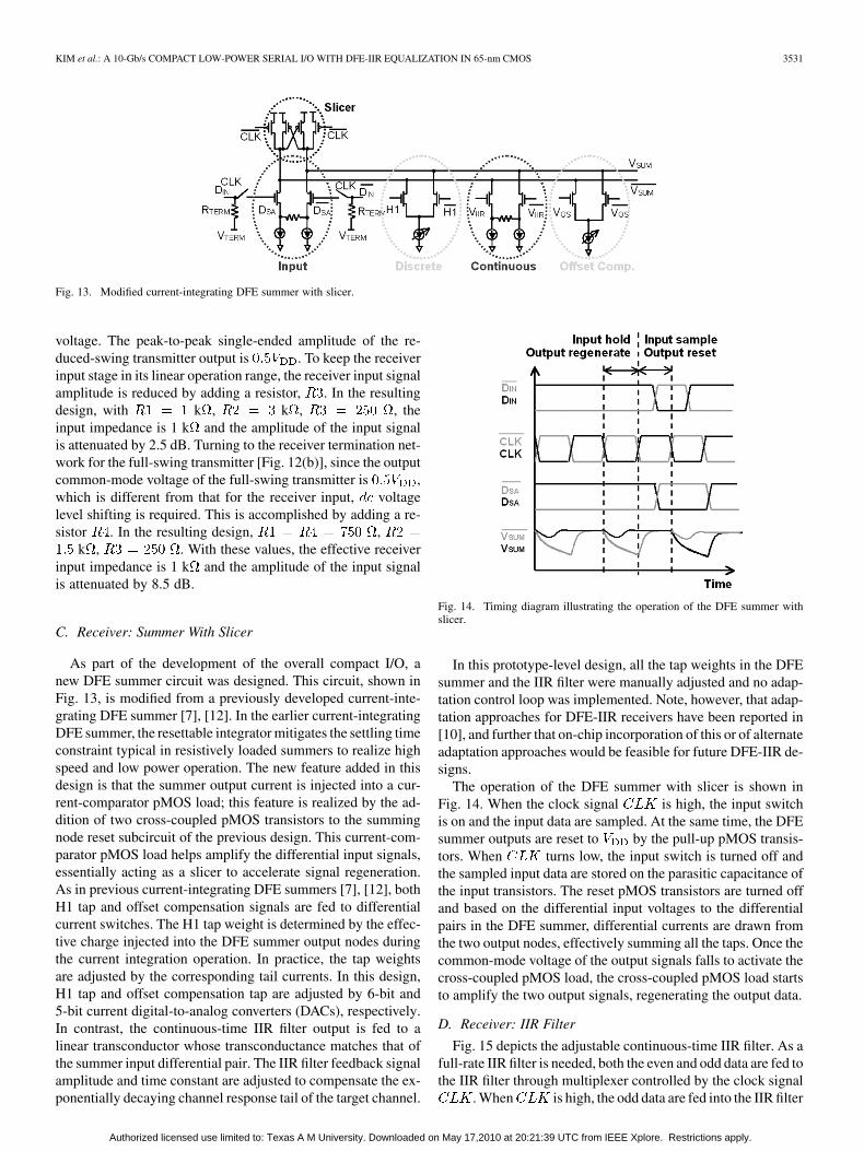
Fig. 13. Modified current-integrating DFE summer with slicer.
voltage. The peak-to-peak single-ended amplitude of the re-duced-swing transmitter output is . To keep the receiverinput stage in its linear operation range, the receiver input signalamplitude is reduced by adding a resistor, . In the resultingdesign, with k , k , , theinput impedance is 1 k and the amplitude of the input signalis attenuated by 2.5 dB. Turning to the receiver termination net-work for the full-swing transmitter [Fig. 12(b)], since the outputcommon-mode voltage of the full-swing transmitter is ,which is different from that for the receiver input, voltagelevel shifting is required. This is accomplished by adding a re-sistor . In the resulting design, ,
k , . With these values, the effective receiverinput impedance is 1 k and the amplitude of the input signalis attenuated by 8.5 dB.
C. Receiver: Summer With Slicer
As part of the development of the overall compact I/O, anew DFE summer circuit was designed. This circuit, shown inFig. 13, is modified from a previously developed current-inte-grating DFE summer [7], [12]. In the earlier current-integratingDFE summer, the resettable integrator mitigates the settling timeconstraint typical in resistively loaded summers to realize highspeed and low power operation. The new feature added in thisdesign is that the summer output current is injected into a cur-rent-comparator pMOS load; this feature is realized by the ad-dition of two cross-coupled pMOS transistors to the summingnode reset subcircuit of the previous design. This current-com-parator pMOS load helps amplify the differential input signals,essentially acting as a slicer to accelerate signal regeneration.As in previous current-integrating DFE summers [7], [12], bothH1 tap and offset compensation signals are fed to differentialcurrent switches. The H1 tap weight is determined by the effec-tive charge injected into the DFE summer output nodes duringthe current integration operation. In practice, the tap weightsare adjusted by the corresponding tail currents. In this design,H1 tap and offset compensation tap are adjusted by 6-bit and5-bit current digital-to-analog converters (DACs), respectively.In contrast, the continuous-time IIR filter output is fed to alinear transconductor whose transconductance matches that ofthe summer input differential pair. The IIR filter feedback signalamplitude and time constant are adjusted to compensate the ex-ponentially decaying channel response tail of the target channel.
Fig. 14. Timing diagram illustrating the operation of the DFE summer withslicer.
In this prototype-level design, all the tap weights in the DFEsummer and the IIR filter were manually adjusted and no adap-tation control loop was implemented. Note, however, that adap-tation approaches for DFE-IIR receivers have been reported in[10], and further that on-chip incorporation of this or of alternateadaptation approaches would be feasible for future DFE-IIR de-signs.
The operation of the DFE summer with slicer is shown inFig. 14. When the clock signal is high, the input switchis on and the input data are sampled. At the same time, the DFEsummer outputs are reset to by the pull-up pMOS transis-tors. When turns low, the input switch is turned off andthe sampled input data are stored on the parasitic capacitance ofthe input transistors. The reset pMOS transistors are turned offand based on the differential input voltages to the differentialpairs in the DFE summer, differential currents are drawn fromthe two output nodes, effectively summing all the taps. Once thecommon-mode voltage of the output signals falls to activate thecross-coupled pMOS load, the cross-coupled pMOS load startsto amplify the two output signals, regenerating the output data.
D. Receiver: IIR Filter
Fig. 15 depicts the adjustable continuous-time IIR filter. As afull-rate IIR filter is needed, both the even and odd data are fed tothe IIR filter through multiplexer controlled by the clock signal
. When is high, the odd data are fed into the IIR filter
Authorized licensed use limited to: Texas A M University. Downloaded on May 17,2010 at 20:21:39 UTC from IEEE Xplore. Restrictions apply.

3532 IEEE JOURNAL OF SOLID-STATE CIRCUITS, VOL. 44, NO. 12, DECEMBER 2009
Fig. 15. Continuous-time IIR filter with adjustable time constant and signalamplitude.
and when is low, the even data are fed into the IIR filter. Tomatch the IIR filter response function with the exponentially de-caying channel response tail (Fig. 9), both the output amplitudeand the filter time constant of the IIR filter need to be adjusted.This tunability is implemented using adjustable resistor , ad-justable capacitor and adjustable current . More specif-ically, the filter’s time constant is adjusted using and .Filter differential output amplitude is adjusted using and
. When the differential output amplitude is changed, the filteroutput common-mode voltage remains constant. In this design,
and are implemented by on-chip components and have1-bit and 5-bit resolution respectively. The 3 most significantbits (MSBs) and 2 least significant bits (LSBs) of are imple-mented with thick-oxide decoupling capacitors and higher-res-olution vertical metal-insulator-metal capacitors, respectively.With the parasitic effects, the time constant covers atuning range of 0.5 UI to 10 UI. The adjustable current isachieved with off-chip current supply, but of course could beimplemented with on-chip DAC in a future design. The outputcommon-mode voltage is maintained at the same level as theinput stage of the DFE summer, namely .
E. Receiver: Double-Regenerating Latch
The output from the DFE summer with slicer is furtherregenerated by a high-speed double-regenerating latch shownin Fig. 16. This latch has two cascaded differential regeneratingstages that achieve higher speed and sensitivity than a staticCMOS latch. Fig. 17 depicts its operation. When the clocksignal is high, the output signals of the first stage areprecharged to . In the second stage, the pMOS transistorsare turned off, so this stage just retains its output at levels in-dicative of the previous bit decision. When goes low, thefirst stage is turned on and begins to regenerate the input signalby the cross-coupled pMOS load. At the same time, the outputcommon-mode voltage of the first stage falls, which then turnson the input transistors of the second stage. When the outputof the first stage is regenerated to a sufficiently high level, thelogical state of second stage is switched. Since the second stagehas cross-coupled nMOS transistors, its output is amplified withadditional regeneration. This latch is particularly useful whenreceiving a weakly regenerating signal from the summer withslicer. In such a case, the first stage of the latch regenerates at
Fig. 16. Double-regenerating latch.
Fig. 17. Timing diagram illustrating the operation of the double-regeneratinglatch.
the same time as the summer with slicer so that the regenerationspeed is improved. The transistors in the second stage are sizedsuch that its rail-to-rail CMOS output has a crossing voltagelevel appropriate for driving nMOS differential current switchesin the current-mode logic (CML) DFE feedback circuits, whicheliminates the need for a CMOS-to-CML converter.
V. IMPLEMENTATIONS
The compact I/O with the DFE-IIR receiver described inSection IV was designed and fabricated in IBM’s 65-nm bulkCMOS technology. To evaluate the performance, stand-alonetransmitters and receivers were implemented, includingfull-swing and reduced-swing transmitters, 5-Gb/s and 10-Gb/sDFE-IIR receivers, as well as 5-Gb/s and 10-Gb/s conventional2-tap DFE receivers. To improve testability, 50- input termi-nation was used for all receiver stand-alone sites instead of thehigh-impedance termination discussed in Section III. In addi-tion to stand-alone receivers and transmitters, a large integratedtransmitter-channel-receiver test site was also implemented.The goal of the integrated test site was to evaluate the compactI/O design in the context of channels emulating those of thetarget silicon carrier application. The die micrograph of thisintegrated test site is shown in Fig. 18. In this site, the channelsconnecting the transmitters and receivers were realized usingon-chip back-end wire, and were designed to match the mea-sured channel characteristics of silicon carrier transmissionlines. Due to lack of thick metals in the CMOS back-endprocess, the emulated channels are differential microstrip struc-tures with parameters designed to match the frequency rolloffcharacteristics of the silicon carrier channels. In total, the largetest site included 12 individual transmitters (some full-swingand some reduced-swing) and 12 individual receivers (splitbetween DFE-IIR and conventional 2-tap DFE instances, withsome of each targeting 5 Gb/s and some 10 Gb/s operation),
Authorized licensed use limited to: Texas A M University. Downloaded on May 17,2010 at 20:21:39 UTC from IEEE Xplore. Restrictions apply.

KIM et al.: A 10-Gb/s COMPACT LOW-POWER SERIAL I/O WITH DFE-IIR EQUALIZATION IN 65-nm CMOS 3533
Fig. 18. Die micrograph of the integrated transmitter-channel-receiver test site.
connected by a variety of channels with lengths ranging from2 mm to 40 mm. In this site, the transmitters and receivers areterminated with low impedance and high impedance, respec-tively, as presented in Section IV. In this prototype, half-ratereceiver clock signals are from off chip and no on-chip eyemonitor was implemented. Five 25-mm channels are groupedtogether so that crosstalk effects can be measured and studied.The full-swing transmitter layout and the DFE-IIR receiverlayout are shown as insets in Fig. 18. The transmitter core,consisting of buffers, latches, and drivers, occupies an area of
m m. The DFE-IIR receiver core, consisting oftermination network, DFE summers, IIR filter, latches, currentDACs, and buffers, occupies an area of m m. Theinclusion of 2-tap DFE receiver blocks enables direct compar-ison between a conventional DFE approach and the DFE-IIRapproach. Finally, an on-chip test structure was also added toallow characterization of the BEOL channel characteristics toenable assessment of the match between the characteristicsof the on-chip channels and those of the target silicon carrierchannels.
VI. EXPERIMENTAL RESULTS
A. Measurements of Stand-Alone Receivers
The measurement of the stand-alone DFE-IIR receiver showsthat it has an input sensitivity of 64 mVppd at 10 Gb/s for abit-error rate (BER) of better than . It operates error-freeup to 13 Gb/s with clean input data.
The equalization capabilities of the DFE-IIR receiver werefirst tested over 30 , 40 , and 50 traces on a high-qualityboard made from Nelco4000-13SI material. Fig. 19(a) and (b)shows the frequency responses and normalized pulse responsesof the channels, respectively. The channels have smoothfrequency rolloff characteristics and exponentially decayinglong response tails similar to those expected in silicon carrierchannels (Fig. 4). Including 2 dB of loss from the test setup,the channels losses are 15.5 dB, 19.6 dB and 23.2 dB at 5 GHz,respectively. Fig. 20 shows the measured receiver bathtubcurves when equalizing 10-Gb/s PRBS7 data transmitted withan amplitude of 600 mVppd over these carrier-like channels[8]. For the 30 , 40 , and 50 channels, at a BER ,the DFE-IIR receiver produced 71%, 57%, and 45% horizontaleye openings, respectively. Note that these measurements do
Fig. 19. Channel characteristics of 30 , 40 , and 50 traces on a Nelco4000-13SI board. (a) Transfer functions. (b) Normalized pulse responses.
Fig. 20. Measured BER bathtub curve after equalizing 10-Gb/s PRBS7 datapassed over the 30 , 40 , and 50 traces characterized in Fig. 19. Horizontaleye openings at BER � �� are reported.
not include recovered clock jitter from a CDR, which was notimplemented in this work. In the center of the eye, data errorrate much less than is achieved. The power consump-tion of the DFE-IIR receiver was 6.8 mA from a 1-V supply(0.68 mW/Gb/s). The power breaks down as follows: 20% fromthe DFE summers with slicers, 25% from the latches, 50% fromthe clock buffers, and 5% from the IIR filter, current DACs andbiasing circuitry.
In a second equalization experiment, 700 mVppd data wastransmitted over a 16 Tyco legacy backplane channel with twodaughter cards. Fig. 21 illustrates the channel characteristics,including frequency response and normalized pulse response.Compared to silicon carrier channels, this 16 Tyco legacybackplane channel has much less smooth frequency rolloff and
Authorized licensed use limited to: Texas A M University. Downloaded on May 17,2010 at 20:21:39 UTC from IEEE Xplore. Restrictions apply.

3534 IEEE JOURNAL OF SOLID-STATE CIRCUITS, VOL. 44, NO. 12, DECEMBER 2009
Fig. 21. Channel characteristics of a 16 Tyco legacy backplane with twodaughter cards. (a) Transfer function. (b) Normalized pulse response.
Fig. 22. Measured BER bathtub curve after equalizing 10-Gb/s PRBS7 datapassed over the 16 Tyco backplane characterized in Fig. 21.
pulse response characteristics, mainly due to significant signalreflections from via stubs in the channel. Again including
2 dB of loss from the test setup, this channel shows 27 dBof loss at 5 GHz. The measured bathtub curve of Fig. 22shows that the DFE-IIR receiver recovers 10-Gb/s PRBS7 datatransmitted over the Tyco backplane channel with a horizontaleye opening of 28% at a BER of . In this experiment, thepower consumption of the DFE-IIR receiver was approximately7 mW from a 1-V supply. This demonstrates the potential ofthe DFE-IIR receiver for low-power backplane equalization inaddition to silicon carrier applications.
Besides equalizing the aforementioned channels with theDFE-IIR receiver, equalization experiments over the same
TABLE ISUMMARY OF STAND-ALONE RECEIVER TEST RESULTS
channels were also performed with a conventional 2-tap DFEreceiver. To allow clear comparisons to be made, the con-ventional 2-tap DFE was implemented using the same basecomponents and power consumption level as the DFE-IIRreceiver. Table I summarizes 10-Gb/s equalization results of theDFE-IIR receiver and 2-tap DFE receiver over various chan-nels [8]. The addition of the IIR filter improved performanceover all tested channels, highlighting the effectiveness of thisequalization scheme.
The stand-alone full-swing and reduced-swing transmitterswere demonstrated to be fully functional up to 10.8 Gb/s.
B. Measurements of Transmitter-Channel-Receiver Test Site
Before equalization experiments on the integrated trans-mitter-channel-receiver test site were performed, the on-chipchannel measurement test structure, whose die micrographis shown on the left side of Fig. 23, was measured. This teststructure, which includes de-embedding structures and BEOLtransmission lines, yielded data enabling extrapolation of S21characteristics for the 25-mm and 40-mm BEOL channelsrealized in the transmitter-channel-receiver test site. Theseextrapolated values are compared with their measured siliconcarrier counterparts in Fig. 23. It can be seen that the emulatedand silicon carrier channels exhibit similar frequency rolloffbehavior, though the carrier channels exhibit a few more dBinsertion loss than the BEOL channels.
Fig. 24 shows the experimental setup. All measurementswere performed on-wafer using high-speed probes. Full-ratedata were generated using a pulse pattern generator and passedto the transmitters on the test site chip. The same full-rate clockused to time the pulse pattern generator was divided to producethe half-rate clock required for the receivers. Adjustable delaylines were used to compensate for skew in the data and clockpaths to optimize the receiver performance. On the integratedtest site chip, the transmitters send full-rate data through theon-chip channels, and the received data are equalized by thehalf-rate receivers. Both half-rate outputs from the receiverwere monitored using error detectors. Serial data providedfrom a computer and controlled through a GUI, are used toprogram the DFE tap weights and offset compensation and
Authorized licensed use limited to: Texas A M University. Downloaded on May 17,2010 at 20:21:39 UTC from IEEE Xplore. Restrictions apply.

KIM et al.: A 10-Gb/s COMPACT LOW-POWER SERIAL I/O WITH DFE-IIR EQUALIZATION IN 65-nm CMOS 3535
Fig. 23. Die micrograph of on-chip channel characterization macro and extrapolated channel data compared with silicon carrier data.
Fig. 24. Test setup for the integrated transmitter-channel-receiver test site.
to select transmitter and receiver from the twelve individualtransmitter-channel-receiver sites.
The equalization results of a PRBS7 data pattern for allthe individual sites are summarized in Fig. 25, which showsmeasured maximum data rates for 15% horizontal eye openingat a BER and the I/O power efficiency (includingtransmitter and receiver) at maximum data rate. This integratedtest site has various combinations of transmitter, channel, ESDand receiver. Successful equalization has been demonstratedacross wide range of channels. Over a 40-mm link with 19-dBrolloff at 4.45 GHz, the 1-V transmitter-receiver pair operatesat 8.9 Gb/s with a 15% eye opening while consuming 17 mW(5.4 mW from the receiver and 11.6 mW from the transmitter)yielding a 1.9-mW/Gb/s power efficiency. When equalizingdata transmitted over a 25-mm link, the DFE-IIR achieves9.5-Gb/s maximum data rate, higher than the 6.7-Gb/s max-imum data rate achieved by a 2-tap DFE, validating DFE-IIR’ssuperior performance as compared to conventional DFE. Addi-tionally, a DFE-IIR receiver with a 550-fF input ESD protectiondevice is shown to equalize a 17-mm channel with a 35% eyeopening at 10 Gb/s. These results demonstrate the feasibility ofthe DFE-IIR for use in low-power compact silicon carrier linkreceivers.
C. Crosstalk Measurements
Crosstalk experiments were performed on the group of five25-mm channels shown on the top of the test site micrograph inFig. 18. The crosstalk experiment setup is depicted in Fig. 26.The channel under test is surrounded by two aggressor channels.
The aggressor channels can be individually turned on and offby the enable signals, ( 1, 2, 3). The two aggressorchannels share clock and data inputs while the channel undertest has independent clock and data. For crosstalk experiments,to remove signal correlations between aggressor channels andthe channel under test, two aggressor channels and the channelunder test are fed with a PRBS31 data pattern and a PRBS7 datapattern, respectively. The relative clock phase between the twoclock signals to aggressor channels and channel under test canbe tuned so that the crosstalk effect under various relative clockskews can be studied.
By measuring and comparing the maximum data rates of thechannel under test with aggressor channels turned on and off,the effect of crosstalk can be evaluated and studied. However,when aggressor channels are turned on, effects like clock cou-pling, data coupling, and supply ripple can also influence themaximum data rate achievable for the channel under test, andthus must be evaluated to determine whether or not measure-ment results reflect true crosstalk-driven impairment. Controlexperiments were performed on the test site to explore this ques-tion, with the results showing only slight impact from these ef-fects on the link performance. The wire-to-wire crosstalk fromadjacent channels is therefore the primary source of the perfor-mance degradation observed in the crosstalk experiments.
Table II summarizes measured maximum data rates of fourchannels with various aggressor channels. With aggressorchannels turned on, the measured channel maximum data ratesdecrease, with the amount of the decrease depending on thenumber of aggressor channels and the amplitudes of data trans-mitted on the channels. For instance, without any aggressorchannels turned on, Channel I, which transmits full-swingdata and is equalized by a DFE-IIR receiver, can operate upto 9 Gb/s. The maximum data rate drops to 8.8 Gb/s with onereduced-swing aggressor channel turned on and further drops to8.6 Gb/s with two reduced-swing aggressor channels turned on.In another crosstalk experiment, Channel II, which transmitsreduced-swing data and is equalized by a DFE-IIR receiver,can operate up to 6.9 Gb/s without any aggressor channelsturned on. With one full-swing aggressor channel turned on,the maximum data rate drops to 6 Gb/s and further drops to4.8 Gb/s with two full-swing aggressor channels turned on,demonstrating more crosstalk effects than the first experiments.Note that in this test site, no extra shielding between adjacentchannels was added so that the crosstalk effects measured here
Authorized licensed use limited to: Texas A M University. Downloaded on May 17,2010 at 20:21:39 UTC from IEEE Xplore. Restrictions apply.

3536 IEEE JOURNAL OF SOLID-STATE CIRCUITS, VOL. 44, NO. 12, DECEMBER 2009
Fig. 25. Summary of integrated transmitter-channel-receiver test site results.
Fig. 26. Crosstalk experiment setup.
Fig. 27. Measured horizontal eye opening of the channel under test with var-ious aggressor clock delays.
reflect worst-case carrier routing; clearly, such shielding in thecarrier channels could be introduced to ameliorate crosstalk-in-duced degradation.
Crosstalk effects depend not only on aggressor channelsignal amplitude but also on relative phase difference betweenaggressor and test channel data. Fig. 27 shows the horizontaleye openings of 4.8-Gb/s data transmitted over channel IIIwith two aggressor channels turned on at various aggressorclock delays. With a 0.5-UI aggressor clock delay, the dataeye is closed and the data eye is increased to 14.5% when theaggressor clock is delayed by 1 UI. Since the skew betweenchannels is expected to be small in the target application, thedata presented in Table II were measured with zero aggressorclock delay.
TABLE IISUMMARY OF MEASURED CHANNEL MAXIMUM DATA RATES
WITH VARIOUS AGGRESSOR CHANNELS
VII. CONCLUSION
A compact I/O with a power-efficient DFE-IIR receivertargeting high-speed serial I/O for dense silicon carrier linksis reported. Based on silicon carrier channel characteristics,low-impedance transmitter and high-impedance receiver ter-minations and DFE-IIR based receiver equalization approachare adopted. In the receiver, a modified DFE with a contin-uous-time IIR feedback was developed for lossy channels withlong pulse response tail requiring multi-tap DFE for ISI cancel-lation. Because it does not include a high tap-count DFE, thisequalizer consumes less area and power than would be requiredwith a conventional approach. Equalization capabilities ofthis DFE-IIR receiver were successfully demonstrated over arange of channels, including smoothly varying PCB channelswith more than 20-dB losses and a legacy backplane channelwith 27-dB loss. Furthermore, the compact I/O operates overvarious on-chip emulated silicon carrier channels ranging from2 mm to 40 mm; for example, over a 40-mm on-chip emulatedchannel, a transmitter-receiver pair operates at 8.9 Gb/s with1.9 mW/Gb/s power efficiency. These results validate the useof the DFE-IIR for serial I/O in advanced silicon packagingtechnologies.
Authorized licensed use limited to: Texas A M University. Downloaded on May 17,2010 at 20:21:39 UTC from IEEE Xplore. Restrictions apply.

KIM et al.: A 10-Gb/s COMPACT LOW-POWER SERIAL I/O WITH DFE-IIR EQUALIZATION IN 65-nm CMOS 3537
ACKNOWLEDGMENT
The authors would like to thank C. Patel, M. Beakes, D.Beisser, K. Jenkins, B. Parker, A. Rylyakov, D. Kuchta, A.Natarajan, X. Gu, D. Kam, and Z. Deniz for technical support,and S. Gowda and M. Soyuer for managerial support.
REFERENCES
[1] J. Knickerbocker, C. Patel, P. Andry, C. Tsang, B. Paivikki, E. Sprogis,G. Hua, R. Horton, R. Polastre, S. Wright, and J. Cotte, “3-D silicon in-tegration and silicon packaging technology using silicon through-vias,”IEEE J. Solid-State Circuits, vol. 41, no. 8, pp. 1718–1725, Aug. 2006.
[2] T. Beukema, M. Sorna, K. Selander, S. Zier, B. L. Ji, P. Murfet, J.Mason, W. Rhee, H. Ainspan, B. Parker, and M. Beakes, “A 6.4-Gb/sCMOS SerDes core with feed-forward and decision-feedback equal-ization,” IEEE J. Solid-State Circuits, vol. 40, no. 12, pp. 2633–2645,Dec. 2005.
[3] R. Payne, P. Landman, B. Bhakta, S. Ramaswamy, S. Wu, J. D. Powers,M. U. Erdogan, A. L. Yee, R. Gu, L. Wu, Y. Xie, B. Parthasarathy,K. Brouse, W. Mohammed, K. Heragu, V. Gupta, L. Dyson, and W.Lee, “A 6.25-Gb/s binary transceiver in 0.13-�m CMOS for serialdata transmission across high loss legacy backplane channels,” IEEEJ. Solid-State Circuits, vol. 40, no. 12, pp. 2646–2657, Dec. 2005.
[4] K. Krishna, D. A. Yokoyama-Martin, A. Caffee, C. Jones, M.Loikkanen, J. Parker, R. Segelken, J. L. Sonntag, J. Stonick, S. Titus,D. Weinlader, and S. Wolfer, “A multigigabit backplane transceivercore in 0.13-�m CMOS with a power-efficient equalization architec-ture,” IEEE J. Solid-State Circuits, vol. 40, no. 12, pp. 2658–2666,Dec. 2005.
[5] J. Bulzacchelli, M. Meghelli, S. Rylov, W. Rhee, A. Rylyakov, H.Ainspan, B. Parker, M. Beakes, A. Chung, T. Beukema, P. Pepelju-goski, L. Shan, Y. Kwark, S. Gowda, and D. Friedman, “A 10-Gb/s5-tap DFE/4-tap FFE transceiver in 90-nm CMOS technology,” IEEEJ. Solid-State Circuits, vol. 41, no. 12, pp. 2885–2900, Dec. 2006.
[6] A. Rylyakov, “An 11 Gb/s 2.4 mW half-rate sampling 2-tap DFE re-ceiver in 65 nm CMOS,” in Symp. VLSI Circuits Dig. Tech. Papers, Jun.2007, pp. 272–273.
[7] T. Dickson, J. Bulzacchelli, and D. Friedman, “A 12-Gb/s 11-mW half-rate sampled 5-tap decision feedback equalizer with current-integratingsummers in 45-nm SOI CMOS technology,” IEEE J. Solid-State Cir-cuits, vol. 44, no. 4, pp. 1298–1305, Apr. 2009.
[8] Y. Liu, B. Kim, T. Dickson, J. Bulzacchelli, and D. Friedman, “A10 Gb/s compact low-power serial I/O with DFE-IIR equalization in65 nm CMOS,” in IEEE ISSCC Dig. Tech. Papers, Feb. 2009, pp.182–183.
[9] E. Mensink, D. Schinkel, E. Klumperink, E. van Tuijl, and B. Nauta,“A 0.28 pJ/b 2 Gb/s/ch transceiver in 90 nm CMOS for 10 mm on-chipinterconnects,” in IEEE ISSCC Dig. Tech. Papers, Feb. 2007, pp.414–415.
[10] P. Crespo and M. Honig, “Pole-zero decision feedback equalizationwith a rapidly converging adaptive IIR algorithm,” IEEE J. Sel. AreasCommun., vol. 9, pp. 817–829, Aug. 1991.
[11] K. Wong, H. Hatamkhani, M. Mansuri, and C. Yang, “A 27-mW 3.6Gb/s I/O transceiver,” IEEE J. Solid-State Circuits, vol. 39, no. 4, pp.602–612, Apr. 2004.
[12] M. Park, J. Bulzacchelli, M. Beakes, and D. Friedman, “A 7 Gb/s 9.3mW 2-tap current-integrating DFE receiver,” in IEEE ISSCC Dig. Tech.Papers, Feb. 2007, pp. 230–231.
Byungsub Kim (S’06) was born in Busan, Korea. Hereceived the B.S. degree in electronic and electricalengineering from Pohang University of Science andTechnology, and the M.S. degree in electrical engi-neering and computer science from the Massachu-setts Institute of Technology, Cambridge, where heis currently pursuing the Ph.D. degree.
In the summers of 2006 and 2007, he was an internat the IBM T. J. Watson Research Center, YorktownHeights, NY, where he developed DFE-IIR architec-tures and circuits for a compact I/O.
Mr. Kim was a co-recipient of the Beatrice Winner Award for Editorial Ex-cellence at the 2009 IEEE International Solid-State Circuits Conference.
Yong Liu (S’03–M’07) received the B.S. and M.S.degrees in electrical engineering from TsinghuaUniversity, Beijing, China, in 2000 and 2003,respectively, and the Ph.D. degree from HarvardUniversity, Cambridge, MA, in 2007. His Ph.D. workexamined applications of CMOS ICs in medicineand biotechnology by directly interfacing CMOS ICswith biological systems. Specifically, he developedCMOS ICs in conjunction with microfluidic systemsto magnetically manipulate individual biologicalcells for cell sorting applications and a CMOS RF
biosensor utilizing NMR for medical diagnostics in a portable platform.He is currently with the IBM T. J. Watson Research Center, Yorktown
Heights, NY. In 2001, he was with Tsinghua Tongfang Microelectronics Co.,working on the second-generation Chinese RF ID card. In 2005 and 2006, hewas with the Mixed-Signal Communications IC Group at IBM T. J. WatsonResearch Center as a summer intern. In November 2007, he joined the IBMT. J. Watson Research Center, where he is involved with the development ofhigh-speed and low-power data links for conventional wireline communicationsystems as well as emerging silicon packaging technologies (silicon carrierlinks and 3-D silicon integration). He has 16 publications, three U.S. patents,and three patents filed.
Dr. Liu was the recipient of the Seagate Scholarship, Motorola Scholarship,Second Prize in the China National Graduate EDA Competition, and AnalogDevices Outstanding Student Designer Award. He was a co-recipient of theBeatrice Editorial Excellence Award in the 2009 IEEE International Solid-StateCircuits Conference.
Timothy O. Dickson (S’01–M’06) received dualB.Sc. degrees in electrical and computer engineeringwith highest honors from the University of Floridain 1999. He completed the M.Eng. degree at theUniversity of Florida in 2002 and the Ph.D. degree atthe University of Toronto in 2006, both in electricalengineering. His Ph.D. work was in the area ofserial transceivers operating up to 80 Gb/s in SiGeBiCMOS technologies, focusing on the developmentof low-noise and low-power design methodologies.
In September 2006, he joined the IBM T. J. WatsonResearch Center in Yorktown Heights, NY, where he is involved with the devel-opment of low-power serial transceivers. He is also an Adjunct Assistant Pro-fessor at Columbia University where he teaches graduate level courses in analogand RF circuit design. His research interests include circuits and semiconductortechnologies for high-speed wireline and mm-wave applications.
Dr. Dickson was named an undergraduate University Scholar by the Univer-sity of Florida in 1999, and was an Edward S. Rogers, Sr Scholar during hisdoctoral work at the University of Toronto. He received the Best Student PaperAward at the 2004 VLSI Circuits Symposium in Honolulu, HI, and was a co-re-cipient of the Beatrice Winner Award for Editorial Excellence at the 2009 IEEEInternational Solid-State Circuits Conference. He is currently a member of theTechnical Programming Committee for the IEEE Compound Semiconductor In-tegrated Circuit Symposium.
John F. Bulzacchelli (S’92–M’02) was born inNew York, NY, in 1966. He received the S.B., S.M.,and Ph.D. degrees in electrical engineering fromthe Massachusetts Institute of Technology (MIT),Cambridge, in 1990, 1990, and 2003, respectively.
From 1988 to 1990 he was a co-op student atAnalog Devices, Wilmington, MA, where he in-vented a new type of delay-and-phase-locked loopfor high-speed clock recovery. From 1992 to 2002he conducted his doctoral research at the IBM T.J. Watson Research Center, Yorktown Heights, NY,
in a joint study program between IBM and MIT. In his doctoral work, hedesigned and demonstrated a superconducting bandpass delta-sigma modulatorfor direct A/D conversion of multi-GHz RF signals. In 2003 he became aResearch Staff Member at this same IBM location, where his primary job is thedesign of mixed-signal CMOS circuits for high-speed data communications.He also maintains strong interest in the design of circuits in more exploratorytechnologies. He holds two U.S. patents.
Authorized licensed use limited to: Texas A M University. Downloaded on May 17,2010 at 20:21:39 UTC from IEEE Xplore. Restrictions apply.
3538 IEEE JOURNAL OF SOLID-STATE CIRCUITS, VOL. 44, NO. 12, DECEMBER 2009
Dr. Bulzacchelli received the Jack Kilby Award for Outstanding StudentPaper at the 2002 IEEE International Solid-State Circuits Conference (ISSCC)and was a co-recipient of the Beatrice Winner Award for Editorial Excellenceat the 2009 ISSCC.
Daniel J. Friedman (S’91–M’92) received the Ph.D.degree in engineering science from Harvard Univer-sity, Cambridge, MA, in 1992.
After completing consulting work at MIT LincolnLabs and postdoctoral work at Harvard in imagesensor design, he joined the IBM Thomas J. WatsonResearch Center, Yorktown Heights, NY, in 1994.His initial work at IBM was the design of analogcircuits and air interface protocols for field-poweredRFID tags. In 1999, he turned his focus to analogcircuit design for high-speed serializer/deserializer
macros. Since June 2000, he has managed a team of mixed-signal circuitdesigners, with recent focus on serial data communication and clock synthesisapplications. In addition to circuits papers on serial links and PLLs, he haspublished articles on imagers and RFID, and he holds more than 20 patents.His current research interests include high-speed I/O design, PLL design, andcircuit/system approaches for variability compensation.
Authorized licensed use limited to: Texas A M University. Downloaded on May 17,2010 at 20:21:39 UTC from IEEE Xplore. Restrictions apply.