
3498 IEEE TRANSACTIONS ON MICROWAVE …users.ece.gatech.edu/etentze/TMTT_2005_Canceller.pdffering...
11
3498 IEEE TRANSACTIONS ONMICROWAVE THEORY AND TECHNIQUES,VOL. 53, NO. 11, NOVEMBER 2005 Analysis and Design of an Interference Canceller for Collocated Radios Anand Raghavan, Student Member, IEEE, Edward Gebara, Member, IEEE, Emmanouil M. Tentzeris, Senior Member, IEEE, and Joy Laskar, Fellow, IEEE Abstract—An active interference cancellation scheme is pre- sented to mitigate interference between Bluetooth and wireless local area network (IEEE 802.11 b) radios operating in close proximity. This method is extensible to other mutually inter- fering radio devices. A reference signal correlated to the original interferer is used to generate a cancellation signal by means of amplitude and phase alignment, and filtration. The filter employed emulates the coupling channel responsible for interference. An implementation of this procedure in 0.18- m Si-complementary metal–oxide–semiconductor (CMOS) integrated-circuit (IC) tech- nology is also presented. The circuits fabricated are tunable and are controlled by a closed-loop adaptive process including an error minimization method. The cancellation system designed achieves 15–30 dB of interference suppression for different cases. A total power of 14 mW is dissipated by the CMOS ICs designed. Index Terms—Active circuits, adaptive control, band-limited signals, interference suppression, phase shifters, spread-spectrum communication. I. INTRODUCTION A STEADY growth in the assimilation of wireless net- working devices into the corporate and personal environ- ment has been seen in recent years. The increased utilization of the industrial, scientific, and medical (ISM) bands is no coincidence since most of these devices rely on the unlicensed portion of the spectrum. While sharing of the spectrum and unlicensed access benefits the end-user, thereby facilitating increased services; it raises questions about network perfor- mance in a densely populated frequency space. Lately, these questions have received recognition, and mechanisms that deter interoperability are better understood. The existence of a wide range of commercial products based on wireless local area networks (WLANs) and wireless personal area networks (WPANs) calls the authors’ attention to their co- existence concerns. Short-range remote signaling devices using the Bluetooth standard [1] and longer range wireless data de- vices adhering to the IEEE 802.11 b/g standard [2] are numerous and present an example of this problem. Their functions are complementary in nature, and they both use spread-spectrum communication techniques, yet, their deployment in close prox- imity can and often does result in mutual performance degrada- tion. The Bluetooth environment, for instance, is analyzed and Manuscript received April 7, 2005; revised August 30, 2005. The authors are with the Georgia Electronic Design Center, Department of Electrical and Computer Engineering, Georgia Institute of Technology, Atlanta, GA 30308 USA and also with Quellan Inc., Atlanta, GA 30308 USA (e-mail: [email protected]). Digital Object Identifier 10.1109/TMTT.2005.859042 simulated with models of the medium access control (MAC) and physical layer (PHY) to predict such a performance loss in [3]. The impairment of IEEE 802.11 devices in the presence of Bluetooth interference is quantified in [4]. Bluetooth systems conforming to the specifications of IEEE 802.15 and WLAN systems utilizing IEEE 802.11 b standards both operate in the 2.4-GHz ISM band. While the former relies on a frequency-hop- ping spread-spectrum (FHSS) scheme, the latter may use either an FHSS or a direct-sequence spread-spectrum (DSSS) tech- nique. Often, when operating under closely spaced conditions, the transmitted signals from these devices may collide in both time and frequency causing a reduction in the signal-to-interfer- ence ratio (SIR) at the receiver of either system. Early findings [5] indicate that performance degradation of both systems in terms of throughput is severe when the interferers are physically located within 2 m of each other, insignificant beyond 10 m, and moderate for intermediate ranges. Naturally, this is undesirable, and methods to understand and mitigate such interference form the focus of this paper. Various methods have been suggested to combat the coexis- tence problem in the 2.4-GHz band, as outlined in [6]. These range from complex time-division multiple-access (TDMA) schemes that involve load-dependent queuing and scheduling algorithms to other MAC or driver layer solutions. However, most software layer approaches disallow simultaneous opera- tion or otherwise compromise the performance capabilities of one of the transmitting systems. Since interference is a physical phenomenon associated with the wireless RF channel and is characterized and measured in the PHY layer, a solution consti- tuted in the PHY addresses the problem nearest the source. The methods proposed in this paper are entirely PHY layer driven and do not impair the inherent abilities of either system. The cost to be paid is manifested as increased silicon and higher power consumption in the reception and decoding circuitry. In Section II, the theoretical underpinnings of the problem are examined in brief. This, in conjunction with measured results, helps formulate the goal of this study. Subsequently, in Section III, the interference suppression system is developed by analysis of noise mechanisms. System control issues are also addressed. An implementation of this procedure using 0.18- m Si-complementary metal–oxide–semiconductor (CMOS) in- tegrated-circuit (IC) technology is presented in Section IV, along with results from their measurement. Alternative circuit solutions are discussed wherever feasible. Finally, in Section V, possible extensions of the proposed interference cancellation scheme to other applications are summarily discussed. 0018-9480/$20.00 © 2005 IEEE
-
Upload
nguyentuong -
Category
Documents
-
view
225 -
download
4
Transcript of 3498 IEEE TRANSACTIONS ON MICROWAVE …users.ece.gatech.edu/etentze/TMTT_2005_Canceller.pdffering...

3498 IEEE TRANSACTIONS ON MICROWAVE THEORY AND TECHNIQUES, VOL. 53, NO. 11, NOVEMBER 2005
Analysis and Design of an InterferenceCanceller for Collocated Radios
Anand Raghavan, Student Member, IEEE, Edward Gebara, Member, IEEE,Emmanouil M. Tentzeris, Senior Member, IEEE, and Joy Laskar, Fellow, IEEE
Abstract—An active interference cancellation scheme is pre-sented to mitigate interference between Bluetooth and wirelesslocal area network (IEEE 802.11 b) radios operating in closeproximity. This method is extensible to other mutually inter-fering radio devices. A reference signal correlated to the originalinterferer is used to generate a cancellation signal by means ofamplitude and phase alignment, and filtration. The filter employedemulates the coupling channel responsible for interference. Animplementation of this procedure in 0.18- m Si-complementarymetal–oxide–semiconductor (CMOS) integrated-circuit (IC) tech-nology is also presented. The circuits fabricated are tunable andare controlled by a closed-loop adaptive process including an errorminimization method. The cancellation system designed achieves15–30 dB of interference suppression for different cases. A totalpower of 14 mW is dissipated by the CMOS ICs designed.
Index Terms—Active circuits, adaptive control, band-limitedsignals, interference suppression, phase shifters, spread-spectrumcommunication.
I. INTRODUCTION
ASTEADY growth in the assimilation of wireless net-working devices into the corporate and personal environ-
ment has been seen in recent years. The increased utilizationof the industrial, scientific, and medical (ISM) bands is nocoincidence since most of these devices rely on the unlicensedportion of the spectrum. While sharing of the spectrum andunlicensed access benefits the end-user, thereby facilitatingincreased services; it raises questions about network perfor-mance in a densely populated frequency space. Lately, thesequestions have received recognition, and mechanisms that deterinteroperability are better understood.
The existence of a wide range of commercial products basedon wireless local area networks (WLANs) and wireless personalarea networks (WPANs) calls the authors’ attention to their co-existence concerns. Short-range remote signaling devices usingthe Bluetooth standard [1] and longer range wireless data de-vices adhering to the IEEE 802.11 b/g standard [2] are numerousand present an example of this problem. Their functions arecomplementary in nature, and they both use spread-spectrumcommunication techniques, yet, their deployment in close prox-imity can and often does result in mutual performance degrada-tion. The Bluetooth environment, for instance, is analyzed and
Manuscript received April 7, 2005; revised August 30, 2005.The authors are with the Georgia Electronic Design Center, Department of
Electrical and Computer Engineering, Georgia Institute of Technology, Atlanta,GA 30308 USA and also with Quellan Inc., Atlanta, GA 30308 USA (e-mail:[email protected]).
Digital Object Identifier 10.1109/TMTT.2005.859042
simulated with models of the medium access control (MAC)and physical layer (PHY) to predict such a performance lossin [3]. The impairment of IEEE 802.11 devices in the presenceof Bluetooth interference is quantified in [4]. Bluetooth systemsconforming to the specifications of IEEE 802.15 and WLANsystems utilizing IEEE 802.11 b standards both operate in the2.4-GHz ISM band. While the former relies on a frequency-hop-ping spread-spectrum (FHSS) scheme, the latter may use eitheran FHSS or a direct-sequence spread-spectrum (DSSS) tech-nique. Often, when operating under closely spaced conditions,the transmitted signals from these devices may collide in bothtime and frequency causing a reduction in the signal-to-interfer-ence ratio (SIR) at the receiver of either system. Early findings[5] indicate that performance degradation of both systems interms of throughput is severe when the interferers are physicallylocated within 2 m of each other, insignificant beyond 10 m, andmoderate for intermediate ranges. Naturally, this is undesirable,and methods to understand and mitigate such interference formthe focus of this paper.
Various methods have been suggested to combat the coexis-tence problem in the 2.4-GHz band, as outlined in [6]. Theserange from complex time-division multiple-access (TDMA)schemes that involve load-dependent queuing and schedulingalgorithms to other MAC or driver layer solutions. However,most software layer approaches disallow simultaneous opera-tion or otherwise compromise the performance capabilities ofone of the transmitting systems. Since interference is a physicalphenomenon associated with the wireless RF channel and ischaracterized and measured in the PHY layer, a solution consti-tuted in the PHY addresses the problem nearest the source. Themethods proposed in this paper are entirely PHY layer drivenand do not impair the inherent abilities of either system. Thecost to be paid is manifested as increased silicon and higherpower consumption in the reception and decoding circuitry.
In Section II, the theoretical underpinnings of the problemare examined in brief. This, in conjunction with measuredresults, helps formulate the goal of this study. Subsequently, inSection III, the interference suppression system is developed byanalysis of noise mechanisms. System control issues are alsoaddressed. An implementation of this procedure using 0.18- mSi-complementary metal–oxide–semiconductor (CMOS) in-tegrated-circuit (IC) technology is presented in Section IV,along with results from their measurement. Alternative circuitsolutions are discussed wherever feasible. Finally, in Section V,possible extensions of the proposed interference cancellationscheme to other applications are summarily discussed.
0018-9480/$20.00 © 2005 IEEE

RAGHAVAN et al.: ANALYSIS AND DESIGN OF INTERFERENCE CANCELLER FOR COLLOCATED RADIOS 3499
II. PROBLEM FORMULATION
A. Theoretical Description
Bluetooth uses a Gaussian frequency-shift keying (GFSK)continuous phase modulation scheme with a modulation indexof 0.3 and a bandwidth bit-period product of 0.5. A symbol rateof 1 MS/s over any of 79 RF channels in the 2.4–2.4835 GHzband makes it effectively narrow band for the purposes of ourproblem. The pseudorandom hopping sequence that defines thechannel has a maximum hop rate of 1600 hops/s. The trans-mitter Gaussian filter spreads each data bit over two symboldurations, causing intersymbol interference (ISI). The trans-mitted power level is usually 0 dBm (1 mW), though as muchas 20 dBm is allowed. WLAN devices using the IEEE 802.11b standard operate by various modulation schemes, dependingon the data rate. They may use differential binary phase-shiftkeying (DBPSK), differential quaternary phase-shift keying(DQPSK), or complementary code keying (CCK). The mod-ulated data is spread by an 11-bit Barker sequence entailing a22-MHz channel bandwidth. The transmission channel may beone of three nonoverlapping channels over the same 2.4-GHzband. A maximum transmit power of 20 dBm (100 mW) ispossible. Channel overlap in time is, thus, likely. MAC layermechanisms in each system are well documented, and furtherdescriptions are available from various sources, such as [7].
The theory surrounding the performance criteria of an IEEE802.11 network in the presence of Bluetooth interferers is vast,and a few key results quantifying this effect are reproduced here.Packet error rate (PER) and number of retransmissions (RT) aretaken as performance parameters, and the probability of a col-lision is denoted as . A collision is said to occur when anIEEE 802.11 b packet is unrecoverable because of a Bluetoothinterferer. If packets are transmitted and represents aPER threshold, it may be shown, as in [8], that
(1)
where is one of and denotes probability.Using the standard error function when is very large, we mayapproximate the binomial distribution. An expected PER lessthan 8% is required by IEEE 802.11 b. Therefore, the probabilitythat the network is free of impairment may be calculated by set-ting the PER threshold at 0.08 in (1). The threshold condition forwhich the WLAN network is said to be significantly impaired issomewhat arbitrary and has been previously assumed to be 0.2.As noted before, a number of RTs may be required to success-fully transmit an IEEE 802.11 b packet from the access point tothe station. If is a threshold for RT, the probability that thisis not exceeded is calculated as the geometric distribution [9]
(2)
The mean and standard deviation of RT are easily calculated.In evaluating the coexistence scenario, a WLAN station and
access point separated by distance are considered with uni-formly distributed Bluetooth piconets surrounding the station.If is the interference-to-signal power ratio threshold beyond
Fig. 1. Bluetooth and WLAN packet transmission timing diagram.
which the WLAN signal is jammed, and and are theIEEE 802.11 and Bluetooth transmit powers, then
(3)
is the normalized interference-to-signal threshold. Further, thearea around the station within a radius whereinterference occurs, is determined by methods similar to Jakes’multipath fading calculations [10]. Some mathematical deliber-ation is necessary [8] to show that
(4)
This is valid in the limiting case where is very large. Here,is the standard deviation of a log-normally distributed
random variable representing the interference-to-signal ratioand is the path loss exponent of the shadowing model used toperform the calculation. Therefore, given typical values of var-ious parameters, interference areas can be found. For instance,
dBm, dBm, m, an acceptableinterference-to-signal ratio threshold dB [11], officebuilding conditions of , and dB [12]yield m .
A simple timing diagram for packet transmission in Bluetoothand WLAN networks is shown is Fig. 1. If is the timeslot duration for Bluetooth, is the packet transmissionduration for WLAN ( s, s),is the transmission time for Bluetooth, and is the offsetbetween the two transmissions, the probability of overlaps intime between the two interfering systems is given by
(5)
The probability of frequency collisions is similarly calcu-lable. Finally, if the probability of activity in a single Bluetoothpiconet is assumed to be independent and identicallydistributed for all piconets, and is the expected number ofBluetooth interferers with an interference level , then the totalprobability of time–frequency collisions is derived [8] as
(6)
(7)

3500 IEEE TRANSACTIONS ON MICROWAVE THEORY AND TECHNIQUES, VOL. 53, NO. 11, NOVEMBER 2005
Fig. 2. Coupling characteristics between closely spaced antennas.
where is a loading factor for the Bluetooth piconets. Hence,we may infer that for typical values of parameters noted beforeand path loss exponent of 4, the probability of collision isgreater than 10% for networks with light Bluetooth traffic andgreater than 40% for networks with heavy Bluetooth traffic. In-terference is, thus, a pressing concern.
B. Measurement and Characterization
Since the goal of this paper is separate from the derivation ofclosed-form analytical solutions to the interference problem, apractical case will be examined. Situations where multiple radiotransceivers are located on the same platform in communica-tion products are increasingly prevalent. In the special case thatboth radios are collocated and required to operate simultane-ously from the same device, the Bluetooth transmitters are wellwithin the interference area of the WLAN receiver as describedin the previous analytical treatment of the problem. To demon-strate this, various paired patch antenna structures were fabri-cated on FR-4 material. These were characterized for operationin the 2.4-GHz band and able to transmit IEEE 802.11 b/g andBluetooth data. The antennas were separated on the board bydistances ranging from to , where is the wavelengthof the carrier radiation. These correspond to distances less than0.1 m at 2.4 GHz, implying that the likelihood of interferenceis very high and the severity enough to compromise the suc-cessful recovery of desired data. The characteristics of the elec-tromagnetic radiation between the antennas were measured andthe -parameters are plotted in Fig. 2. The plot shows the cou-pling between the two antennas for different spacing conditions.
As evidenced by the graph, the coupling (or relative interfer-ence level) varies from 13 to 27 dB. Maximum couplingoccurs at the spacing as expected. Such interferencelevels are formidable and reduce the SIR at the target receiver.A WLAN receiver has a recommended sensitivity of 75 dBm,and numbers from 85 to 95 dBm are typical. Considering
that the transmit level from a Bluetooth radio can be as high as20 dBm (with power control) or 0 dBm, signal levels at the re-ceiver may be drowned in a sea of noise under these conditions.For receive systems with extreme sensitivity requirements suchas global positioning system (GPS), a lower power radiator inits vicinity may act as an aggressor if transmitting in the samefrequency band, or even by spectral fallout.
An understanding of the nature of interference in the con-text of our problem is necessary for achieving any success insuppressing it. We may loosely refer to the undesired energy inthe receive antenna of the victim (i.e., WLAN) system as noise.Based on this definition, the noise may be separately treatedas in-band and out-of-band noise. Since the transmission fre-quency band of 83.5 MHz width is identical for the two ra-dios, the in-band noise pours energy into frequencies that eithertransmitter may use. Whereas out-of-band noise also degradesradio performance, it may be rejected by appropriately filteringat the transmit or receive end. This is possible owing to the factthat no desired information is contained in the spectrum outsidethe band of interest. However, out-of-band noise is not entirelytrivial for the following two reasons.
• Though a transmit channel is precisely defined, it is physi-cally impossible to limit radiation without spreading noiseinto sidebands, depending on the transmit spectral mask.Sideband signals, thus, are a potential source of interfer-ence.
• Out-of-band noise at the boundary of a band is as impor-tant as noise in-band because of the nonrectangular natureof filters.
Out-of-band noise, being a minor cause for concern andperipheral to our problem, will be ignored. The nature of a PHYlayer solution, therefore, depends squarely on the behavior ofin-band noise. Successful negotiation of in-band noise requiresfurther categorization of noise as broad-band (white) andband-limited (colored). Broad-band noise in the time domain isa random process of statistically uncorrelated impulse energies.This implies nondeterministic behavior and no coordinationwith any identifiable source. Band-limited noise, on the otherhand, is deterministic in nature. It is statistically correlated intime to a particular source. Since the aggressing transmitteris the source, and the coupling channel is the means of timecorrelation, this deterministic noise is clearly the offshoot ofan intentional signal radiation. Furthermore, the in-band noisemay be modeled as the superposition of a broad-band and aband-limited component.
Traditionally, most high-frequency radio systems are plaguedonly by broad-band noise. As such, their circuit implementa-tions are designed to alleviate white noise only. To minimizeconfusion, the band-limited component of in-band noise willhenceforth be referred to as the “interferer.” The interferencecancellation scheme suggested in this paper allows us tosuppress the above-mentioned interferer while maintainingadequate broad-band noise performance. The analytical back-ground of the scheme along with the description of a system toimplement it is discussed in the following section.

RAGHAVAN et al.: ANALYSIS AND DESIGN OF INTERFERENCE CANCELLER FOR COLLOCATED RADIOS 3501
Fig. 3. Adaptive noise suppression scheme processing discrete-time signalsand noise.
III. SYSTEM ANALYSIS
A. Cancellation Approach
The interference cancellation method employed by us relieson subtracting an internally generated interferer from the signalreceived at the victim antenna. When the subtraction and in-termediate filtration is done adaptively, superior signal-to-noiseratio (SNR) may be obtained compared to direct filtration ofthe received signal [13]. As such, it is a dual-input closed-loopadaptive noise suppression scheme. A schematic, representativeof the cancellation process, is shown in Fig. 3.
Referring to the figure, the victim antenna receives a signal
(8)
where is the information-bearing signal of interest,is a narrow-band interferer, and is broad-band noise. Thetwo noise terms are not correlated to the signal or to each other.Specifically, the expectation
(9)
for all .The cancellation unit receives another input that is
given by
(10)
where and are narrow-band and broad-band noiseterms, respectively. Whereas, the two broad-band noise termsare uncorrelated to any source by definition, and is un-correlated to the signal , the two narrow-band noise termsare correlated to each other. All signals under consideration arewide-sense stationary. In general, the cross correlation betweenthe two narrow-band noise terms is unknown and given by
(11)
for a lag . Traditionally, is processed by an adaptive filterto produce an output signal
(12)
where represents the adaptable weights of the filter. Theoutput of the cancellation unit is, thus, the error signal
(13)
where is the narrow-band correlated noise contribution ofto the output, and is the total broad-band noise at
the victim antenna. If the control mechanism is able to dynam-ically converge and achieve cancellation, the condition
(14)
will ensure success.The implementation described here differs from the general
case above in that the cross correlation of (11) is not completelyunknown. Since the aggressor antenna, which is the source ofcorrelated noise, is assumed to be located in the immediate prox-imity of the victim, the cancellation unit has access to a scaledand delayed version of . Though this approach may slightlyaffect the aggressor, it obviates the need for large and complextapped-delay finite impulse response (FIR) filters. However, itmust be noted that is defined not only by the source an-tenna but also by the wireless coupling channel. This channel isnot expressible analytically in closed form and, therefore, stillneeds to be emulated in order to process . Under the oper-ating conditions considered above, measurements show that thecoupling channel is largely stationary in its characteristics for agiven configuration of the interferers, forming the basis for thedesign of a simple emulation filter. The filter is endowed withlimited tunability to combat dynamic environments.
In either case discussed above, the only correlation among theinputs to the canceller being between and , we maywrite the mean power of the output as
(15)
Maximizing the output SNR, therefore, requires minimizingthe left-hand side of (15). Usually, this is accomplished in adap-tive filtering schemes by using gradient-descent- or random-search-based control algorithms [14]. This study utilizes a gra-dient descent procedure for adaptation.
Examining the above correlation chain in continuous time,and preserving the same notations as in (8)–(15), we may write
(16)
where is the Fourier transform of the filter and isthat of the narrow-band noise input to the cancellation unit. Thisis possible only when the filter is linear and the coupling channelemulated by the filter is assumed linear time invariant. When thefilter output is sampled at time , this yields
(17)

3502 IEEE TRANSACTIONS ON MICROWAVE THEORY AND TECHNIQUES, VOL. 53, NO. 11, NOVEMBER 2005
Fig. 4. Physical sources of correlated noise in a radio system and itssuppression.
as the output power due to the interferer. In addition, the av-erage power of the total broad-band noise at the victim antennais given by
(18)
where is the power spectral density of . Therefore,the SNR before and after cancellation may be expressed as
(19)
Here, the powers are measured at a time , the numeratorsare constant, and the frequency domain representation ofis obtained from (17).
B. Proposed Canceller Unit
The cancellation technique employed, outlined earlier in [15],is schematically represented in Fig. 4. Shown here are sourcesof deterministic interferers acting by various physical mecha-nisms. The primary media responsible for crosstalk are a sharedconductive substrate and air acting as a channel for antennaradiation.
A downscaled replica of the signal at the aggressing antennais tapped off by the cancellation unit and used as the inputas in (10). The feed-in lines shown in Fig. 4 represent the trans-mission lines from the aggressor and victim antennas, to whichthe alignment/correlation chain interfaces. The alignment/cor-relation chain itself is responsible for emulating the aggressorsignal by appropriately transforming the tapped-off input; thiswill be explained later. This reference input is always accompa-nied by the white noise present in the aggressor and else-where. As long as is very small compared to the transmitlevel in the aggressor, any effect on the Bluetooth transmissionis insignificant. Coupling levels to the victim antenna being lessthan 13 dB, and the voltage level of the tapped-off signal
needs to be less than 2.5% of the Bluetooth transmit level to ac-complish cancellation with a system of unity maximum gain. Acancellation signal is generated by the unit, which is governedby external controls. Combining this signal with the receivedsignal at the victim (i.e.., WLAN) antenna at a 180 phase dif-ferential affects the suggested interference suppression. Loopcancellation methods that are different from our method havebeen used before [16] to generate narrow-band nulls at specificfrequencies to achieve isolation in full-duplex radios. Correla-tion and the generation of a cancellation signal within the unitare performed by gain and phase alignment of the input ,and filtration through defined in (12) and (16). An issueof significance requiring remark here is that our method cre-ates a cancellation notch in-band that is wider compared to theabove-mentioned narrow-band nulls. The method used in [16]is targeted at an adaptive duplexer in a frequency division du-plex (FDD) system. In that method, two separate and indepen-dent nulls are created in the spectrum at the transmit and re-ceive center frequencies. The two nulls separated by a 45-MHzoffset are very narrow single-tone nulls. Besides, there is nooverlap between the transmit and receive frequencies. How-ever, the approach proposed in this study addresses a problemwhere the aggressor and source occupy exactly the same 83.5-MHz-wide band. The cancellation notch can be created overthe whole band and is, thus, independent of both carrier mod-ulation and the aggressor frequency channel in use at any giventime. This is important because very-narrow-band nulls are im-practical in spread-spectrum communication systems owing totheir hopping nature. Furthermore, band limiting through theemulation filter helps prevent the coupled noise from decorre-lating for a larger time interval, allowing easier cancellation,as suggested in [17]. Besides, as noted in [18], some applica-tions may necessitate the use of noncausal filters in the adap-tation path. Deriving the correlated input directly from the ag-gressor, however, negates this requirement since the interfererdoes not reach the victim before it does the cancellation unit.The importance of this stems from the fact that delays cannotbe placed in the primary interference mechanism (air) betweenthe Bluetooth and WLAN radios, thus, making it difficult to vi-olate causality. This, in conjunction with the fact that the carrierfrequencies are much higher than the data rates in our applica-tion, implies that interference suppression may be adequatelyaccomplished by means of gain and phase adjustments, and fil-tration alone.
A prototype of the canceller was constructed on FR-4 mate-rial in keeping with the principles discussed above. A schematicis shown in Fig. 5.
The paired patch antennas of our earlier measurements act astransmitter and receiver in the problem, as illustrated in Fig. 5.Inputs to and outputs from the canceller unit are processed bypower splitting and combining elements along the feed lines.The board shown is constituted of discrete components, thoughthe IC equivalents are also described subsequently. With refer-ence to Fig. 5, the phase aligner, variable gain amplifier (VGA),and bandpass emulation filter form the alignment/correlationchain mentioned earlier. The primary emulation filter serves asa coarse scale model of the coupling/interference channel. This

RAGHAVAN et al.: ANALYSIS AND DESIGN OF INTERFERENCE CANCELLER FOR COLLOCATED RADIOS 3503
Fig. 5. Simplified schematic of the interference cancellation unit.
model is refined by the VGA and phase aligner to accuratelymatch the reference input signal to the source aggressor signal,thereby correlating the two and emulating the channel.
The emulation filter is implemented as an inductance–capaci-tance ( ) filter with a bandpass response, so that the pass bandcoincides with the 83.5-MHz band of interest. It uses a varactordiode in shunt with a high- discrete inductor. The pass bandbeing rather narrow in comparison with the center frequency(2441.75 MHz) necessitates the use of a high- inductor. Fur-ther, the varactor diode implementation of the capacitor allowsvoltage-controlled tunability of the filter characteristic to adjustfor slight channel mismatches. Gain control is through a VGAable to provide voltage gain from 0 to 1 or greater. A 360 con-tinuously variable phase shifter is used to align the phase of thecorrelated sample signal with the interferer.
External control circuitry includes a power detector to esti-mate the energy of the error signal, which is minimized usinga feedback control loop, as indicated by the power detect andnoise minimize control blocks in Fig. 5. The control loop drivesseveral digital-to-analog converters (DACs) that adjust all thevariable components. Since minimizing the error signal is equiv-alent to finding a minimum for the mean output signal energyas shown in (15), a relatively simple procedure is employed.Known pilot signals generated by the VCO in Fig. 5 are in-jected into the canceller unit along with the reference interferer.These pilots occupy extremely narrow bandwidths and are situ-ated outside the edges of the 2.4-GHz band. Not being in-band,they do not affect canceller performance in the region of interest.It is surmised that the spectrum of the coupled signal after can-cellation being smooth, a lowering of energy in-band will corre-spond with energy reduction at the band edge also. Hence, moni-toring and minimizing the energy in the pilot signal at the outputof the canceller is equivalent to minimizing coupling within the
Fig. 6. Out-of-band pilot tones used for cancellation in-band by varying phaseadjustment controls.
band. This, however, does not mean that the cancellation notchis wide enough to cover the whole 2.4-GHz band. Generating awide enough notch requires simultaneously minimizing the en-ergy of both pilots. Precise knowledge of the pilot signals andtheir higher power levels compared to the in-band signals makesthis scheme more robust and easier to implement. The result ofsuch a control mechanism was measured, and an example of thecancellation data within the 2.4-GHz band is shown in Fig. 6.
Various curves in the graph represent different states of thecontroller. As observed from the plot, a phase shift of around90 yields optimum cancellation at one band edge (governedby pilot 1), but a different phase shift optimizes cancellation atthe other edge (governed by pilot 2). The iterative error mini-mization process, however, selects a phase shift of around 70as optimal for the whole band, based on both pilots. The pilotsdepicted in the graph are representative and not exact in powerlevel or frequency.
The canceller features a feedback control mechanism thatoperates using the principle of gradient descent. Here, thecontroller is driven by the measured error energy gradientwith respect to each control variable, after the emulationchannel. During the iterative control process, the error energydescribes a nonnegative error surface along which the controlvariables travel, depending on the adaptation algorithm used[19]. In the control loop designed, a differential steepest de-scent (DSD)-type algorithm [14] was used to determine theabove-mentioned gradient. This is similar to the least meansquares (LMS) approach, except that unlike the latter, where thegradient is estimated during each iteration, the DSD algorithmactually calculates it.
IV. CMOS IC IMPLEMENTATION
The components of the canceller unit described in the pre-vious section were implemented in a standard 0.18- m CMOSIC technology, affording superior integrability into a radiodevice environment. Wireless radio front-end design migratinglargely toward Si-CMOS, this offers the best possibility of
3504 IEEE TRANSACTIONS ON MICROWAVE THEORY AND TECHNIQUES, VOL. 53, NO. 11, NOVEMBER 2005
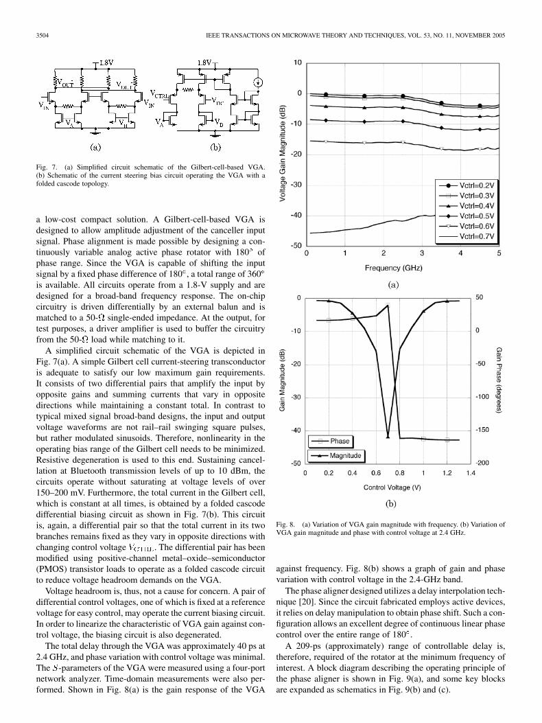
Fig. 7. (a) Simplified circuit schematic of the Gilbert-cell-based VGA.(b) Schematic of the current steering bias circuit operating the VGA with afolded cascode topology.
a low-cost compact solution. A Gilbert-cell-based VGA isdesigned to allow amplitude adjustment of the canceller inputsignal. Phase alignment is made possible by designing a con-tinuously variable analog active phase rotator with 180 ofphase range. Since the VGA is capable of shifting the inputsignal by a fixed phase difference of 180 , a total range of 360is available. All circuits operate from a 1.8-V supply and aredesigned for a broad-band frequency response. The on-chipcircuitry is driven differentially by an external balun and ismatched to a 50- single-ended impedance. At the output, fortest purposes, a driver amplifier is used to buffer the circuitryfrom the 50- load while matching to it.
A simplified circuit schematic of the VGA is depicted inFig. 7(a). A simple Gilbert cell current-steering transconductoris adequate to satisfy our low maximum gain requirements.It consists of two differential pairs that amplify the input byopposite gains and summing currents that vary in oppositedirections while maintaining a constant total. In contrast totypical mixed signal broad-band designs, the input and outputvoltage waveforms are not rail–rail swinging square pulses,but rather modulated sinusoids. Therefore, nonlinearity in theoperating bias range of the Gilbert cell needs to be minimized.Resistive degeneration is used to this end. Sustaining cancel-lation at Bluetooth transmission levels of up to 10 dBm, thecircuits operate without saturating at voltage levels of over150–200 mV. Furthermore, the total current in the Gilbert cell,which is constant at all times, is obtained by a folded cascodedifferential biasing circuit as shown in Fig. 7(b). This circuitis, again, a differential pair so that the total current in its twobranches remains fixed as they vary in opposite directions withchanging control voltage . The differential pair has beenmodified using positive-channel metal–oxide–semiconductor(PMOS) transistor loads to operate as a folded cascode circuitto reduce voltage headroom demands on the VGA.
Voltage headroom is, thus, not a cause for concern. A pair ofdifferential control voltages, one of which is fixed at a referencevoltage for easy control, may operate the current biasing circuit.In order to linearize the characteristic of VGA gain against con-trol voltage, the biasing circuit is also degenerated.
The total delay through the VGA was approximately 40 ps at2.4 GHz, and phase variation with control voltage was minimal.The -parameters of the VGA were measured using a four-portnetwork analyzer. Time-domain measurements were also per-formed. Shown in Fig. 8(a) is the gain response of the VGA
Fig. 8. (a) Variation of VGA gain magnitude with frequency. (b) Variation ofVGA gain magnitude and phase with control voltage at 2.4 GHz.
against frequency. Fig. 8(b) shows a graph of gain and phasevariation with control voltage in the 2.4-GHz band.
The phase aligner designed utilizes a delay interpolation tech-nique [20]. Since the circuit fabricated employs active devices,it relies on delay manipulation to obtain phase shift. Such a con-figuration allows an excellent degree of continuous linear phasecontrol over the entire range of 180 .
A 209-ps (approximately) range of controllable delay is,therefore, required of the rotator at the minimum frequency ofinterest. A block diagram describing the operating principle ofthe phase aligner is shown in Fig. 9(a), and some key blocksare expanded as schematics in Fig. 9(b) and (c).

RAGHAVAN et al.: ANALYSIS AND DESIGN OF INTERFERENCE CANCELLER FOR COLLOCATED RADIOS 3505
Fig. 9. (a) Simplified diagram showing phase shifter operation. (b) Circuitschematic of the modified Gilbert cell (G1 and G2). (c) Schematic of switchingmechanism used to control G1 and toggle extra delay D1.
The portion of the circuit between B and C, as shown inFig. 9(a) forms the core of the phase shifter. The modifiedGilbert cell G2, which is expanded in Fig. 9(b), is configuredsuch that each differential amplifier constituting the cell acceptsa different set of inputs. Whereas one set of inputs arrivesdirectly from B, the other is delayed by the two cascadeddifferential amplifiers (D2 and D3) between B and C. Thecell G2 further sums the currents through each of its halves atthe output node so that it effectively interpolates between thedelays of its inputs.
The exact delay desired is obtained by adjusting the currentsthrough the two halves of G2. This is done by means of a controlvoltage at the folded cascode current biasing circuit of G2 in amanner similar to the VGA.
With reference to Fig. 9(a), is the delay a signal experi-ences while propagating between B and C. This delay is vari-able and controlled by the current steering circuit that biases themodified Gilbert cell G2. It varies between andat the two extremes of the control range. Therefore, the total con-trollable delay range is
(20)
Now, the differential amplifier delay cells D2 and D3 inFig. 9(a) have fixed delays and . The cell G2 interpo-lates between the two paths from B to C so that at one extremeof the control range, the output signal at C is entirely due tothe fast path, and at the other, it is entirely due to the slow paththrough the D2 and D3. Hence, the controllable delay range in(20) above is
(21)
The total gain of D2 and D3 must be unity so that the inputs toG2 differ only in phase but not in amplitude. However, despiteensuring the unity gain criterion, the nature of the interpolatorprevents constant gain across the control range. One method ofsurmounting this is to use dynamic current biasing through thecurrent source. If the tail current through G2 is increased non-linearly through the middle of the bias range, a constant effec-tive transconductance may be obtained. With nonlinear dynamicbiasing through metal–oxide–semiconductor field-effect tran-sistor (MOSFET) devices being difficult to achieve, this methodis abandoned in favor of a simpler solution. Increasing the gainrange of the VGA enough to ascertain that the total gain ofthe system is unity at the middle of the phase control range issufficient.
The total delay range available from the above section of thecircuit was around 150 ps, which corresponds to a phase rangeof 130 at 2.4 GHz. The section of the phase rotator circuit fromA to B contributes the remainder of the phase control range.Again, this portion of the circuit consists of a modified Gilbertcell G1 that receives inputs directly from A and through thedifferential amplifier delay cell D1. G1 is different from G2 inthat each of its differential amplifier halves is constant currentbiased. It does not operate by a current steering mechanism. Theoutputs are summed across the pair of matched load resistors atB. D1 is a unity gain stage providing more than 59 ps of delay.This is a fixed delay that can be turned on or off by a switchingcontrol circuit that biases the two halves of G1. The switchingcircuit is shown expanded in Fig. 9(c) and relies on an externaldigital voltage , that takes values of 0 and 1.8 V. Therefore,if and represent the delay between A and C when D1is switched off or on
(22)
However, the controllable delay range in each case is equalto . The total delay range available over the two modes,which is also the total possible delay range of the entire circuit,is given by
(23)
which is more than the required 209 ps.Another possible approach to designing the phase aligner is
shown in Fig. 10.This involves two independently controllable VGAs andwith voltage gain ranges from 0 to 1 and a quadrature genera-
tion circuit. Assuming a sinusoidal input (ignoring modulation),if and are the gains of the two VGAs, and the frequencyof the input tone, the output is given by
(24)
The output signal can be adjusted to have any amplitude from0 to 1, and any phase shift from 0 to 360 with respect to theinput, by appropriately varying and . The difficulty in this ap-proach stems from the complexity involved in designing a pre-cise high-frequency quadrature generator that functions acrossa frequency band.

3506 IEEE TRANSACTIONS ON MICROWAVE THEORY AND TECHNIQUES, VOL. 53, NO. 11, NOVEMBER 2005
Fig. 10. Alternative scheme for the design of a variable phase shifter.
Fig. 11. Variation of the transmission phase with frequency for the phasealigner at different control voltages.
-parameter and time-domain measurements were per-formed on the phase rotator fabricated. The measured phasevariation at different frequencies as a function of control voltageis shown in Fig. 11. Phase wrapping is employed for ease ofinterpretation.
Generally speaking, for a modulated sinusoid being trans-mitted through a system with a bandpass characteristic, thecarrier is delayed by the phase delay and the modulating databy the group delay. Eliminating phase dispersion, therefore,usually translates to a constant group delay or linear phaseresponse requirement. This is reduced to a triviality in the con-text of the present problem because the bandwidth of interest(83.5 MHz) is very small compared to the center frequency(2.4 GHz). Independent control of the amplitude and phasenecessitates a roughly constant gain characteristic for the phaseshifter with varying control voltage. This, along with phasevariation in-band is illustrated by the measurements shown inFig. 12.
The bandpass emulation filter described earlier is adaptedto the coupling channel. The varactor diode provides a tuningrange of 2.1–2.6 pF controllable in steps of 0.1 pF, allowing a
Fig. 12. In-band (2.4 GHz) variation of gain magnitude and phase with acontrol parameter for the phase shifter.
Fig. 13. Schematic of on-board tunable bandpass emulation filter.
wide range of filter factors. A schematic of the filter with lim-ited tunability is shown in Fig. 13.
As the circuits that constitute the high-frequency path throughthe canceller are of a large delay type, the consequent resis-tance–capacitance time constants introduce many poles inthe alternating current (ac) transfer function. Combined with thecascading of resistively loaded differential amplifier stages, thishas the effect of reducing system ac bandwidth. Fortunately, theextremely narrow-band nature of the aggressor and the victimsignals renders this effect inconsequential. The ac 6-dB voltagegain corner frequencies of the VGA and phase shifter were ap-proximately 6 GHz and 600 MHz, respectively.
The transmission characteristics of the coupling channel,measured before and after cancellation, are shown in Fig. 14. Amaximum cancellation of 30 dB is observed in-band, therebyreducing the interference level from 18 to 48 dB. Whenthe antennas were arranged at a different distance, the couplingwas decreased from 27 to 56.6 dB, implying a total cancel-lation of 29.6 dB. The null created, as noted from the graph, isnarrower in bandwidth than may be desired. Appropriate tuningof the canceller produces a wider band null that provides alower level of cancellation throughout the band, as noted in theprevious section. These numbers directly translate to an SNRimprovement in the victim receiver front-end. The total currentconsumption of the ICs is approximately 7.8 mA.
An active cancellation result reported in [16] shows improvedisolation and reduced transmitter noise leakage into the receiveband in a 2-GHz radio duplexer operating in a FDD scheme.A noise cancellation of up to 37 dB has been reported using

RAGHAVAN et al.: ANALYSIS AND DESIGN OF INTERFERENCE CANCELLER FOR COLLOCATED RADIOS 3507
Fig. 14. Canceller performance showing magnitude of coupling before andafter cancellation for one physical configuration of the aggressor and victim.
Fig. 15. (a) Microphotograph of VGA die for testing. (b) Microphotograph ofphase aligner die for testing. (c) Photograph of canceller on evaluation board.
complex vector attenuators to establish double nulls. However,the narrow-band null created and the reference input source areat different frequencies and do not occupy the same band as inour problem. Photographs of some of the CMOS dice and theboard are shown in Fig. 15.
V. CONCLUSION
An active cancellation technique enabling the coexistence ofcollocated radios has been analyzed. A canceller that providessignificant interference mitigation at a low power cost has beendesigned. The general nature of the cancellation method pro-posed and implemented in this study suits its application to otherradio environments provided the interfering radio systems arein close proximity of each other. Their mutual physical config-uration also needs to be relatively static. These constraints areusually satisfied when the radios are situated on the same de-
vice. In the absence of the latter condition, or when the natureof correlation between the interferer and the reference signal isunknown, correlation must be established by means of an adap-tive FIR filter. Relieving the extremely high-sensitivity GPSreceiver of interference is a promising alternative application.Such interference is found to occur from the global system formobile communications (GSM) (DCS 1800 MHz) transmittersthat use power levels as high as 36 dBm operating in powerclass 3, or 30 dBm in power class 1 [21], in a frequency band200 MHz away. In other devices, high-speed wire line basebanddata transmissions in the vicinity of a GPS receiver may causenoise by spectral fallout.
ACKNOWLEDGMENT
The authors wish to acknowledge Quellan Inc., Atlanta, GA,for their collaboration and support in realizing the system.
REFERENCES
[1] B. P. Crow, I. Widjaja, L. G. Kim, and P. T. Sakai, “IEEE 802.11 wirelesslocal area networks,” IEEE Commun. Mag., vol. 35, no. 9, pp. 116–126,Sep. 1997.
[2] J. C. Haartsen, “The Bluetooth radio system,” IEEE Pers. Commun., vol.7, no. 1, pp. 28–36, Feb. 2000.
[3] Impact of Interference on the Bluetooth Access Control Performance:Preliminary Results, IEEE Standard 802.15/00-322r0, 2000.
[4] Impact of Bluetooth on 802.11 Direct Sequence, IEEE Standard 802.11-98/319, 1998.
[5] SCORT—An Alternative to the Bluetooth SCO Link for Operation in anInterference Environment, IEEE Standard 802.15-01/145r0, 2001.
[6] J. Lansford, A. Stephens, and R. Nevo, “Wi-Fi (802.11b) and Blue-tooth: Enabling coexistence,” IEEE Network, vol. 15, no. 5, pp. 20–27,Sep.–Oct. 2001.
[7] C. F. Chiasserini and R. R. Rao, “Coexistence mechanisms for inter-ference mitigation in the 2.4-GHz ISM band,” IEEE Trans. WirelessCommun., vol. 2, no. 5, pp. 964–975, Sep. 2003.
[8] I. Howitt, “WLAN and WPAN coexistence in UL band,” IEEE Trans.Veh. Technol., vol. 50, no. 4, pp. 1114–1124, Jul. 2001.
[9] R. V. Hogg and E. A. Tanis, Probability and Statistical Inference. NewYork: MacMillan, 1977.
[10] W. C. Jakes, Microwave Mobile Communications. New York: Wiley,1974.
[11] Extension of Bluetooth and 802.11 Direct Sequence Model, IEEE Stan-dard 802.11-98/378, 1998.
[12] T. S. Rappaport, Wireless Communication Principles and Prac-tice. New York: IEEE Press, 1996.
[13] B. Widrow et al., “Adaptive noise canceling: Principles and applica-tions,” Proc. IEEE, vol. 63, no. 12, pp. 1692–1716, Dec. 1975.
[14] B. Widrow and J. McCool, “A comparison of adaptive algorithms basedon the methods of steepest descent and random search,” IEEE Trans.Antennas Propag., vol. AP-24, no. 5, pp. 615–637, Sep. 1976.
[15] A. Raghavan, E. Gebara, M. M. Tentzeris, and J. Laskar, “An activeinterference canceller for multistandard collocated radio,” presented atthe IEEE MTT-S Int. Microwave Symp., Long Beach, CA, Jun. 12–17,2005.
[16] S. Kannangara and M. Faulkner, “Adaptive duplexer for multiband trans-ceiver,” in Proc. Radio Wireless Conf., Boston, MA, Aug. 2003, pp.381–384.
[17] G. Marsh and T. Sutton, “Analog active cancellation of a wireless cou-pled transmit signal,” U.S. Patent 6 539 204, Mar. 25, 2003.
[18] S. Boll and D. Pulsipher, “Suppression of acoustic noise in speech usingtwo microphone adaptive noise cancellation,” IEEE Trans. Acoust.,Speech, Signal Process., vol. ASSP-28, no. 6, pp. 752–753, Dec. 1980.
[19] B. Widrow et al., “Stationary and nonstationary learning characteristicsof the LMS adaptive filter,” Proc. IEEE, vol. 64, no. 8, pp. 1151–1162,Aug. 1976.
[20] B. Razavi, Design of Analog CMOS Integrated Circuits. New York:McGraw-Hill, 2001.
[21] Digital Cellular Telecommunications System (Phase 2+, GSM): RadioTransmission and Reception, ETSI Standard GSM05.05 Version 5.11.1ETS 300 910, 1999.

3508 IEEE TRANSACTIONS ON MICROWAVE THEORY AND TECHNIQUES, VOL. 53, NO. 11, NOVEMBER 2005
Anand Raghavan (S’01) received the B.S. degreein electrical engineering from the Indian Institute ofTechnology, Madras, India, in 2001, the M.S. degreefrom the Georgia Institute of Technology, Atlanta, in2003, and is currently working toward the Ph.D. de-gree at the Georgia Institute of Technology.
His research interests include RF IC design, devicemodeling, and IC design for high-speed and collabo-rative signal-processing applications.
Edward Gebara (M’05) received the B.S. (withhighest honors), M.S., and Ph.D. degrees in electricaland computer engineering from the Georgia Instituteof Technology, Atlanta, in 1996, 1999 and 2003,respectively.
He is currently a Member of Technical Staff withQuellan Inc., Atlanta, GA, where he develops high-performance analog semiconductors that improve thespeed and reach of communication channels in con-sumer, broadcast, enterprise, computing and wirelessmarkets. He is also a research faculty member with
the Georgia Institute of Technology, where he leads the Mixed Signal Teamresearch efforts. The team research interest is to develop the foundation for al-ternate modulation schemes (quadrature amplitude modulation (QAM), opticalsubcarrier multiplexing (OSCM), etc.), equalization techniques, and crosstalkcancellation techniques on pure CMOS applied to next-generation wired andwireless communication. He has authored or coauthored over 50 publications.
Emmanouil M. Tentzeris (SM’03) received theDiploma degree in electrical and computer engi-neering from the National Technical Universityof Athens, Athens, Greece, in 1992, and the M.S.and Ph.D. degrees in electrical engineering andcomputer science from The University of Michiganat Ann Arbor, in 1993 and 1998, respectively.
He is currently an Associate Professor with theSchool of Electrical and Computer Engineering,Georgia Institute of Technology, Atlanta. During thesummer of 2002, he was a Visiting Professor with
the Technical University of Munich, Munich, Germany. He has authored orcoauthored over 170 papers in refereed journals and conference proceedingsand eight book chapters. He has helped develop academic programs in highlyintegrated packaging for RF and wireless applications, microwave MEMS,system-on-package (SOP)-integrated antennas and adaptive numerical electro-magnetics (finite difference time domain (FDTD), multiresolution algorithms).He is the Georgia Tech National Science Foundation (NSF)-Packaging Re-search Center Associate Director for RF Research and the RF Alliance Leader.He is also the Leader of the Novel Integration Techniques Sub-Thrust of theBroadband Hardware Access Thrust of the Georgia Electronic Design Center(GEDC) of the State of Georgia.
Dr. Tentzeris is member of the Technical Chamber of Greece. He was the 1999Technical Program co-chair of the 54th ARFTG Conference, Atlanta, GA. He isthe vice-chair of the RF Technical Committee (TC16) of the IEEE Components,Packaging, and Manufacturing Technology (CPMT) Society. He was the recip-ient of the 2003 IEEE CPMT Outstanding Young Engineer Award, the 2002International Conference on Microwave and Millimeter-Wave Technology BestPaper Award (Beijing, China), the 2002 Georgia Tech-Electrical and ComputerEngineering (ECE) Outstanding Junior Faculty Award, the 2001 ACES Con-ference Best Paper Award, the 2000 NSF CAREER Award, and the 1997 BestPaper Award, International Hybrid Microelectronics and Packaging Society.
Joy Laskar (S’84–M’85–SM’02–F’05) received theB.S. degree (highest honors) in computer engineeringwith math/physics minors from Clemson University,Clemson, SC, in 1985, and the M.S. and Ph.D. de-grees in electrical engineering from the Universityof Illinois at Urbana-Champaign, in 1989 and 1991,respectively.
Prior to joining the Georgia Institute of Tech-nology, Atlanta, in 1995, he held faculty positionswith the University of Illinois at Urbana-Champaignand the University of Hawaii. At the Georgia Insti-
tute of Technology, he holds the Joseph M. Pettit Professorship of Electronicsand is currently the Chair for the Electronic Design and Applications TechnicalInterest Group, the Director of Georgia’s Electronic Design Center, and theSystem Research Leader for the National Science Foundation (NSF) PackagingResearch Center. With the Georgia Institute of Technology, he heads a researchgroup with a focus on integration of high-frequency electronics with opto-elec-tronics and integration of mixed technologies for next-generation wireless andopto-electronic systems. In July 2001, he became the Joseph M. Pettit Professorof Electronics with the School of Electrical and Computer Engineering, GeorgiaInstitute of Technology. He has authored or coauthored over 210 papers. Hehas ten patents pending. His research has focused on high-frequency IC designand their integration. His research has produced numerous patents and transferof technology to industry. Most recently, his research has resulted in theformation of two companies. In 1998, he cofounded the advanced WLAN ICcompany RF Solutions, which is now part of Anadigics. In 2001, he cofoundedthe next-generation interconnect company Quellan Inc., Atlanta, GA, whichdevelops collaborative signal-processing solutions for enterprise applications.
Dr. Laskar has presented numerous invited talks. For the 2004–2006 term, hehas been appointed an IEEE Distinguished Microwave Lecturer for his RecentAdvances in High Performance Communication Modules and Circuits seminar.He was a recipient of the 1995 Army Research Office’s Young InvestigatorAward, 1996 recipient of the National Science Foundation (NSF) CAREERAward, 1997 NSF Packaging Research Center Faculty of the Year, 1998 NSFPackaging Research Center Educator of the Year, 1999 corecipient of the IEEERappaport Award (Best IEEE Electron Devices Society journal paper), thefaculty advisor for the 2000 IEEE Microwave Theory and Techniques Society(IEEE MTT-S) International Microwave Symposium (IMS) Best Student PaperAward, 2001 Georgia Institute of Technology Faculty Graduate Student Mentorof the Year, a 2002 IBM Faculty Award, 2003 Clemson University College ofEngineering Outstanding Young Alumni Award, and 2003 Outstanding YoungEngineer of the IEEE MTT-S.


