32bit SRC with PCM/DSD conversion - Audio Design Guide · SRC Conversion PCM→PCM, DSD →DSD...
80
[AK4137] 015008606-E-00 2015/07 - 1 - 1. General Description The AK4137 is a 2ch digital sample rate converter (SRC). The input sample rate ranges from 8kHz to 768kHz. The output sample rate is from 8kHz to 768kHz. The AK4137 has an internal Oscillator. Therefore it does not need any external master clocks and simplifies a system configuration. The AK4137 is suitable for the application interfacing to different sample rates such as high-end Audio Systems and USB-DACs. It is capable of playing back various audio formats with PCM-DSD data conversion function. 2. Features 2 channels input/output Asynchronous Sample Rate Converter PCM Input Sample Rate Range (FSI): 8kHz~768kHz Output Sample Rate Range (FSO): 8kHz~768kHz Input to Output Sample Rate Ratio: FSO/FSI = 1/6 ~ 24 DSD Input Sample Rate Range (FSI): 2.8224MHz~12.288MHz Output Sample Rate Range (FSO): 2.8224MHz~12.288MHz Input to Output Sample Rate Ratio: FSO/FSI = 1/6 ~ 24 THD+N: Up to −150dB Dynamic Range: 186dB (A-weighted) I/F format: MSB justified, LSB justified, I 2 S compatible and TDM PCM/DSD converter DoP I/F Oscillator for Internal Operation Clock Clock for Master mode: 64/128/192/256/384/512/768fso On-chip X’tal oscillator Digital De-emphasis Filter (32kHz, 44.1kHz, 48kHz) Soft Mute Function SRC Bypass mode (Master/Slave, PCM, DSD) uP Interface: I2C bus/SPI 4-wire Power Supply DVDD: 3.0~3.6V (internal LDO enabled) DVDD: 1.7~1.9V (internal LDO disabled) Operating Temperature: Ta= −40 ~ +105°C Package 48-pin LQFP (0.5mm pitch) 32bit SRC with PCM/DSD conversion AK4137
Transcript of 32bit SRC with PCM/DSD conversion - Audio Design Guide · SRC Conversion PCM→PCM, DSD →DSD...
[AK4137]
015008606-E-00 2015/07 - 1 -
1. General Description
The AK4137 is a 2ch digital sample rate converter (SRC). The input sample rate ranges from 8kHz to 768kHz. The output sample rate is from 8kHz to 768kHz. The AK4137 has an internal Oscillator. Therefore it does not need any external master clocks and simplifies a system configuration. The AK4137 is suitable for the application interfacing to different sample rates such as high-end Audio Systems and USB-DACs. It is capable of playing back various audio formats with PCM-DSD data conversion function.
2. Features
2 channels input/output
Asynchronous Sample Rate Converter
PCM Input Sample Rate Range (FSI): 8kHz~768kHz Output Sample Rate Range (FSO): 8kHz~768kHz
Input to Output Sample Rate Ratio: FSO/FSI = 1/6 ~ 24
DSD Input Sample Rate Range (FSI): 2.8224MHz~12.288MHz Output Sample Rate Range (FSO): 2.8224MHz~12.288MHz
Input to Output Sample Rate Ratio: FSO/FSI = 1/6 ~ 24
THD+N: Up to −150dB
Dynamic Range: 186dB (A-weighted)
I/F format: MSB justified, LSB justified, I2S compatible and TDM
PCM/DSD converter
DoP I/F
Oscillator for Internal Operation Clock
Clock for Master mode: 64/128/192/256/384/512/768fso
On-chip X’tal oscillator
Digital De-emphasis Filter (32kHz, 44.1kHz, 48kHz)
Soft Mute Function
SRC Bypass mode (Master/Slave, PCM, DSD)
uP Interface: I2C bus/SPI 4-wire
Power Supply DVDD: 3.0~3.6V (internal LDO enabled) DVDD: 1.7~1.9V (internal LDO disabled)
Operating Temperature: Ta= −40 ~ +105°C
Package 48-pin LQFP (0.5mm pitch)
32bit SRC with PCM/DSD conversion AK4137
[AK4137]
015008606-E-00 2015/07 - 2 -
3. Table of Contents
1. General Description ............................................................................................................................ 1 2. Features .............................................................................................................................................. 1 3. Table of Contents ................................................................................................................................ 2 4. Block Diagram ..................................................................................................................................... 5 5. Pin Configurations and Functions ....................................................................................................... 6
Pin Functions ..................................................................................................................................... 7
6. Absolute Maximum Ratings ............................................................................................................... 11 7. Recommended Operation Conditions ................................................................................................ 11 8. SRC Characteristics .......................................................................................................................... 12
PCMIN → PCMOUT ...................................................................................................................... 12
PCMIN → DSDOUT ...................................................................................................................... 12
DSDIN → PCMOUT ...................................................................................................................... 13
9. Power Consumptions ........................................................................................................................ 14
Internal LDO Mode .......................................................................................................................... 14
DV18 External Supply Mode ........................................................................................................... 14
10. Filter Characteristics ...................................................................................................................... 15
Sharp Roll-Off Filter Characteristics ............................................................................................... 15
Slow Roll-Off Filter Characteristics ................................................................................................. 16
Short Delay Sharp Roll-Off Filter Characteristics ........................................................................... 17
Short Delay Slow Roll-Off Filter Characteristics ............................................................................. 18
11. DSD Mode Characteristics ............................................................................................................ 19
Sharp Roll-Off Filter Characteristics ............................................................................................... 19
Slow Roll-Off Filter Characteristics ................................................................................................. 19
Short Delay Sharp Roll-Off Filter Characteristics ........................................................................... 20
Short Delay Slow Roll-Off Filter Characteristics ............................................................................. 20
12. Input and Output Examples ........................................................................................................... 21 13. DC Characteristics......................................................................................................................... 23 14. Switching Characteristics .............................................................................................................. 23
Timing Diagrams ............................................................................................................................. 29
15. Functional Descriptions ................................................................................................................. 37
Operation Mode and Setting ........................................................................................................... 37
Power-up Sequence ........................................................................................................................ 38
SRC Bypass Mode .......................................................................................................................... 39
Slave Mode ..................................................................................................................................... 41
Master Mode ................................................................................................................................... 41
X’tal Mode ........................................................................................................................................ 41
System Clock and Audio Interface Format for Input PORT ............................................................ 42
System Clock for Output PORT ...................................................................................................... 46
Audio Interface Format for Output PORT ....................................................................................... 48
Cascade Connection in TDM Mode ................................................................................................ 53
Soft Mute Function .......................................................................................................................... 54
Dither Circuit .................................................................................................................................... 56
Digital Filter...................................................................................................................................... 57
De-emphasis Filter .......................................................................................................................... 57
Regulator ......................................................................................................................................... 57
DSD Mode ....................................................................................................................................... 58
System Reset .................................................................................................................................. 60
Internal Reset Function for Clock Change ...................................................................................... 61
When the frequency of ILRCK at input port is changed without a reset by the PDN pin or RSTN bit
.............................................................................................................................................................. 62
[AK4137]
015008606-E-00 2015/07 - 3 -
When the frequency of OLRCK at output port is changed without a reset by the PDN pin or RSTN
bit .......................................................................................................................................................... 62
Pop Noise Reduction in Sampling Rate Conversion ...................................................................... 63
Input Source Switching (PCM↔DSDI, DoP Mode) ........................................................................ 63
Internal Status Pin ........................................................................................................................... 63
Serial Control Interface ................................................................................................................... 64
Register Map ................................................................................................................................... 68
Grounding and Power Supply Decoupling ...................................................................................... 74
16. Jitter Tolerance .............................................................................................................................. 75 17. Recommended External Circuit .................................................................................................... 76 18. Package ......................................................................................................................................... 78
Outline Dimensions ......................................................................................................................... 78
Material & Lead Finish .................................................................................................................... 78
Marking ............................................................................................................................................ 79
19. Revision History ............................................................................................................................. 79 IMPORTANT NOTICE ........................................................................................................................ 80
[AK4137]
015008606-E-00 2015/07 - 4 -
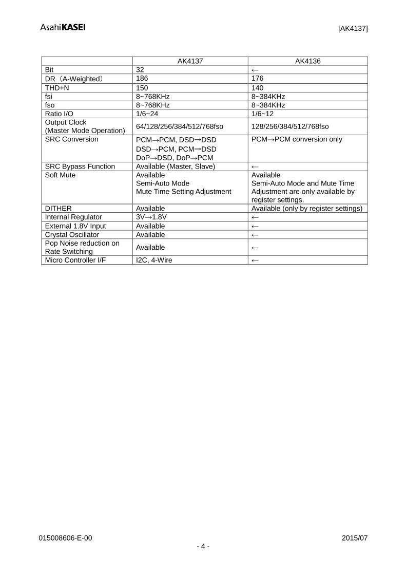
AK4137 AK4136
Bit 32 ←
DR(A-Weighted) 186 176
THD+N 150 140
fsi 8~768KHz 8~384KHz
fso 8~768KHz 8~384KHz
Ratio I/O 1/6~24 1/6~12
Output Clock (Master Mode Operation)
64/128/256/384/512/768fso 128/256/384/512/768fso
SRC Conversion PCM→PCM, DSD→DSD
DSD→PCM, PCM→DSD
DoP→DSD, DoP→PCM
PCM→PCM conversion only
SRC Bypass Function Available (Master, Slave) ←
Soft Mute Available Semi-Auto Mode Mute Time Setting Adjustment
Available Semi-Auto Mode and Mute Time Adjustment are only available by register settings.
DITHER Available Available (only by register settings)
Internal Regulator 3V→1.8V ←
External 1.8V Input Available ←
Crystal Oscillator Available ←
Pop Noise reduction on Rate Switching
Available ←
Micro Controller I/F I2C, 4-Wire ←
[AK4137]
015008606-E-00 2015/07 - 5 -
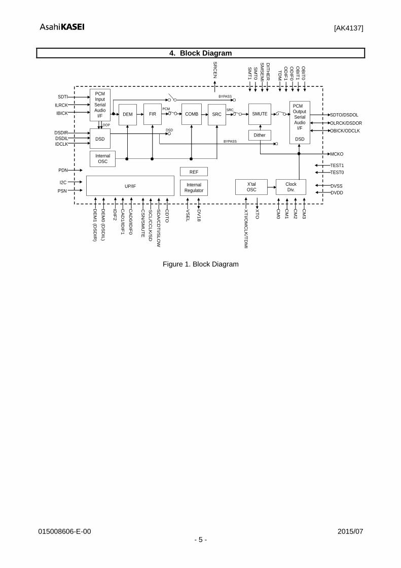
4. Block Diagram
PCM Input Serial Audio
I/F
PCM Output Serial Audio
I/F
DSD
OLRCK/DSDOR
OBICK/ODCLK
SDTO/DSDOL
MCKO
DVDD
Internal OSC
DE
M0
(DS
DIL
)
CA
D0
/IDIF
0
SMUTE
COMB
X’tal OSC
Clock Div.
UP/IF
Internal
Regulator
REF
SRC
DEM
DVSS
FIR
DSD
PCM
BYPASS
SRC
DE
M1
(DS
DIR
)
CA
D1
/IDIF
1
OD
IF0
OD
IF1
SM
SE
MI
DIT
HE
R
SM
T0
SM
T1
TD
M
SR
CE
N
TEST1
TEST0
ILRCK
IBICK
SDTI
PDN
PSN
I2C
Dither
IDIF
2
CS
N/S
MU
TE
SC
L/C
CLK
/SD
SD
A/C
DT
I/SL
OW
VS
EL
DV
18
XT
I/OM
CL
K/T
DM
I
XT
O
CM
0
CM
1
CM
2
OB
IT1
OB
IT0
CD
TO
CM
3
DSD DSDIL
IDCLK
DSDIR
BYPASS
DOP
Figure 1. Block Diagram
[AK4137]
015008606-E-00 2015/07 - 6 -
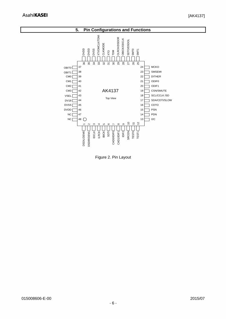
5. Pin Configurations and Functions
DV
DD
38
CM0
36
39
CM1 40
CM2 41
CM3
42
VSEL 43
DV18 44
DVSS 45
DVDD 46
NC 47
NC 48
DV
DD
35
34
TD
M
33
OLR
CK
/DS
DO
R
32
OB
ICK
/OD
CLK
31
30
SM
T1
29
28
XT
O
27
SD
TO
/DS
DO
L
26
1
DS
DIR
/DE
M1
2
IDC
LK
3
ILR
CK
4
IBIC
K
5
SD
TI
6
CA
D0/I
DIF
0
7
CA
D1/I
DIF
1
8
IDIF
2
9
SR
CE
N
10
11
23
22
21
20
19
18
17
16
15
14
13
SMSEMI
DITHER
ODIF0
ODIF1
CSN/SMUTE
SCL/CCLK /SD
SLOW
SDA/CDTI/SLOW
CDTO
PSN
PDN
I2C
AK4137
Top View
TE
ST
1
12
24 MCKO
SM
T0
25
37
DS
DIL
/DE
M0
TE
ST
0
OBIT1
OBIT0
DV
SS
XT
I/O
MC
LK
/TD
MI
CLK
MO
DE
Figure 2. Pin Layout
[AK4137]
015008606-E-00 2015/07 - 7 -
Pin Functions
No. Pin Name I/O Function
1 DSDIL I DSD Data Pin in DSD Mode
DEM0 I De-emphasis Control #0 Pin
2 DSDIR I DSD Data Pin in DSD Mode
DEM1 I De-emphasis Control #1 Pin
3 IDCLK I DSD Clock Pin in DSD Mode
4 ILRCK I L/R Clock Pin in PCM Mode
5 IBICK I Audio Serial Data Clock Pin in PCM Mode
6 SDTI I Audio Serial Data Input Pin in PCM Mode
7 CAD0 I Chip Address 0 Pin in Serial Control Mode
IDIF0 I Digital Input Format 0 Pin in Parallel Control Mode
8 CAD1 I Chip Address 1 Pin in Serial Control Mode
IDIF1 I Digital Input Format 1 Pin in Parallel Control Mode
9 IDIF2 I Digital Input Format 2 Pin in Parallel Control Mode
10 SRCEN O Unlock Status Pin
When the PDN pin= “L”, this pin outputs “H”.
11 TEST0 I Test pin 0. Must be connected to DVSS in normal use.
12 TEST1 I Test pin 1. Must be connected to DVSS in normal use.
13 I2C I Select serial mode
“L”: 4-wire serial Mode ,“H”: I2C Mode
14 PDN I
Power-Down Mode Pin
“H”: Power up,
“L”: Power down reset and initializes the control register.
The AK4137 should be reset once by bringing PDN pin = “L” upon
power-up.
15 PSN I Parallel/Serial Mode Select. “L”: Serial Mode , “H”: Parallel Mode
Note 1. All input pins must not be allowed to float. DVDD must be connected to the same power supply. Note 2. PSN, CM3-0, OBIT1-0, TDM, ODIF1-0, IDIF2-0 and CAD1-0 pin must be changed when the
PDN pin = “L”.
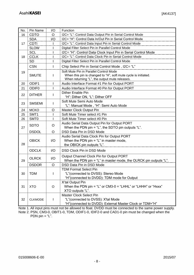
[AK4137]
015008606-E-00 2015/07 - 8 -
No. Pin Name I/O Function
16 CDTO O I2C= “L”: Control Data Output Pin in Serial Control Mode
17
SDA I/O I2C= “H”: Control Data In/Out Pin in Serial Control Mode
CDTI I I2C= “L”: Control Data Input Pin in Serial Control Mode
SLOW I Digital Filter Select Pin in Parallel Control Mode
18
SCL I I2C= “H”: Control Data Clock Input Pin in Serial Control Mode
CCLK I I2C= “L”: Control Data Clock Pin in Serial Control Mode
SD I Digital Filter Select Pin in Parallel Control Mode
19
CSN I Chip Select Pin in Serial Control Mode , I2C= “L”
SMUTE I Soft Mute Pin in Parallel Control Mode
When this pin is changed to “H”, soft mute cycle is initiated. When returning “L”, the output mute releases.
20 ODIF1 I Audio Interface Format #1 Pin for Output PORT
21 ODIF0 I Audio Interface Format #0 Pin for Output PORT
22 DITHER I Dither Enable Pin
“H”: Dither ON, “L”: Dither OFF
23 SMSEMI I Soft Mute Semi Auto Mode
“L”: Manual Mode , “H”: Semi Auto Mode
24 MCKO O Master Clock Output Pin
25 SMT1 I Soft Mute Timer select #1 Pin
26 SMT0 I Soft Mute Timer select #0 Pin
27 SDTO O
Audio Serial Data Output Pin for Output PORT
When the PDN pin = “L”, the SDTO pin outputs “L”.
DSDOL O DSD Data Pin in DSD Mode
28 OBICK I/O
Audio Serial Data Clock Pin for Output PORT
When the PDN pin = “L” in master mode,
the OBICK pin outputs “L”.
ODCLK I/O DSD Clock Pin in DSD Mode
29 OLRCK I/O
Output Channel Clock Pin for Output PORT
When the PDN pin = “L” in master mode, the OLRCK pin outputs “L”.
DSDOR O DSD Data Pin in DSD Mode
30 TDM I
TDM Format Select Pin
“L”(connected to DVSS): Stereo Mode
“H”(connected to DVDD): TDM mode for Output
31 XTO O
X’tal Output Pin
When the PDN pin = “L” or CM3-0 = “LHHL” or “LHHH” or “Hxxx”
XTO outputs “L”.
32 CLKMODE I
Master Clock Select Pin
“L”(connected to DVSS): X'tal Mode
“H”(connected to DVDD): External Master Clock or TDM=”H”
Note 1. All input pins must not be allowed to float. DVDD must be connected to the same power supply. Note 2. PSN, CM3-0, OBIT1-0, TDM, ODIF1-0, IDIF2-0 and CAD1-0 pin must be changed when the
PDN pin = “L”.
[AK4137]
015008606-E-00 2015/07 - 9 -
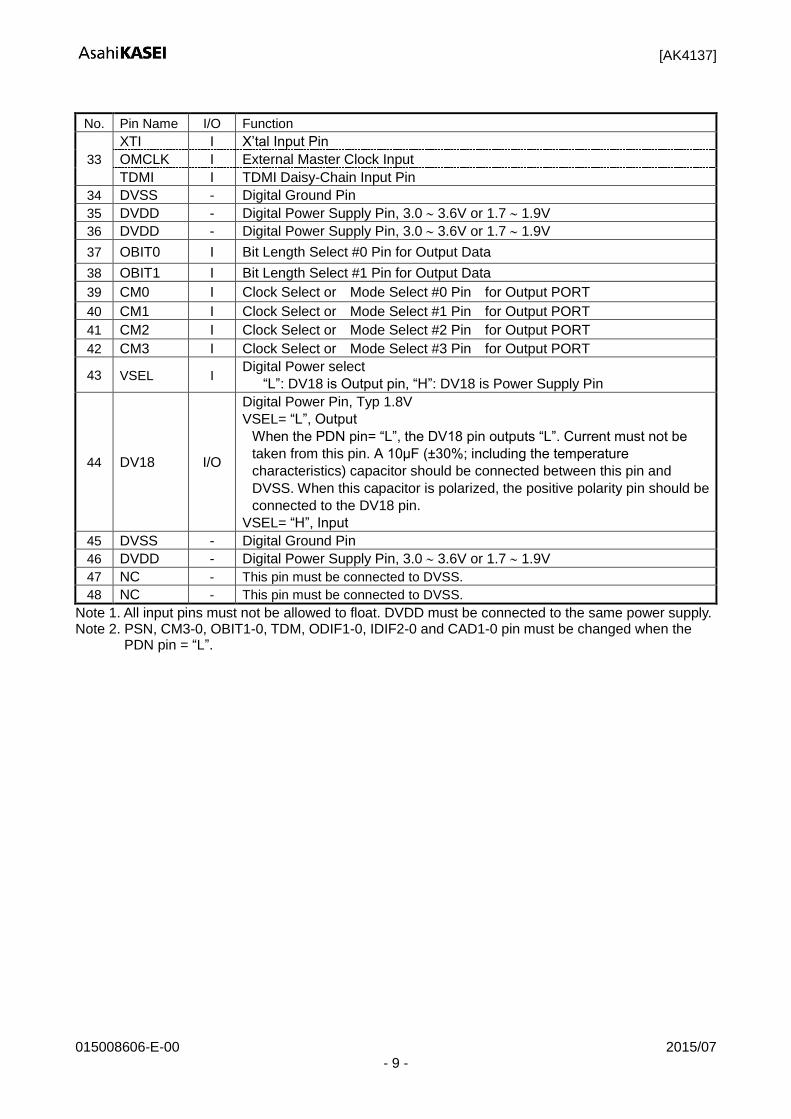
No. Pin Name I/O Function
33
XTI I X’tal Input Pin
OMCLK I External Master Clock Input
TDMI I TDMI Daisy-Chain Input Pin
34 DVSS - Digital Ground Pin
35 DVDD - Digital Power Supply Pin, 3.0 3.6V or 1.7 1.9V
36 DVDD - Digital Power Supply Pin, 3.0 3.6V or 1.7 1.9V
37 OBIT0 I Bit Length Select #0 Pin for Output Data
38 OBIT1 I Bit Length Select #1 Pin for Output Data
39 CM0 I Clock Select or Mode Select #0 Pin for Output PORT
40 CM1 I Clock Select or Mode Select #1 Pin for Output PORT
41 CM2 I Clock Select or Mode Select #2 Pin for Output PORT
42 CM3 I Clock Select or Mode Select #3 Pin for Output PORT
43 VSEL I Digital Power select
“L”: DV18 is Output pin, “H”: DV18 is Power Supply Pin
44 DV18 I/O
Digital Power Pin, Typ 1.8V
VSEL= “L”, Output
When the PDN pin= “L”, the DV18 pin outputs “L”. Current must not be
taken from this pin. A 10μF (±30%; including the temperature
characteristics) capacitor should be connected between this pin and
DVSS. When this capacitor is polarized, the positive polarity pin should be
connected to the DV18 pin.
VSEL= “H”, Input
45 DVSS - Digital Ground Pin
46 DVDD - Digital Power Supply Pin, 3.0 3.6V or 1.7 1.9V
47 NC - This pin must be connected to DVSS.
48 NC - This pin must be connected to DVSS.
Note 1. All input pins must not be allowed to float. DVDD must be connected to the same power supply. Note 2. PSN, CM3-0, OBIT1-0, TDM, ODIF1-0, IDIF2-0 and CAD1-0 pin must be changed when the
PDN pin = “L”.
[AK4137]
015008606-E-00 2015/07 - 10 -
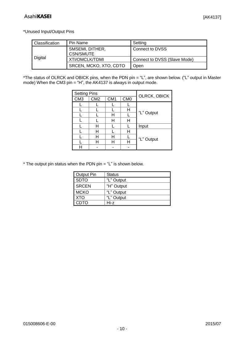
*Unused Input/Output Pins
Classification Pin Name Setting
Digital
SMSEMI, DITHER, CSN/SMUTE
Connect to DVSS
XTI/OMCLK/TDMI Connect to DVSS (Slave Mode)
SRCEN, MCKO, XTO, CDTO Open
*The status of OLRCK and OBICK pins, when the PDN pin = “L”, are shown below. (“L” output in Master mode) When the CM3 pin = “H”, the AK4137 is always in output mode.
Setting Pins OLRCK, OBICK
CM3 CM2 CM1 CM0
L L L L
“L” Output L L L H
L L H L
L L H H
L H L L Input
L H L H
“L” Output L H H L
L H H H
H - - -
* The output pin status when the PDN pin = “L” is shown below.
Output Pin Status
SDTO “L” Output
SRCEN “H” Output
MCKO “L” Output
XTO “L” Output
CDTO Hi-z
[AK4137]
015008606-E-00 2015/07 - 11 -
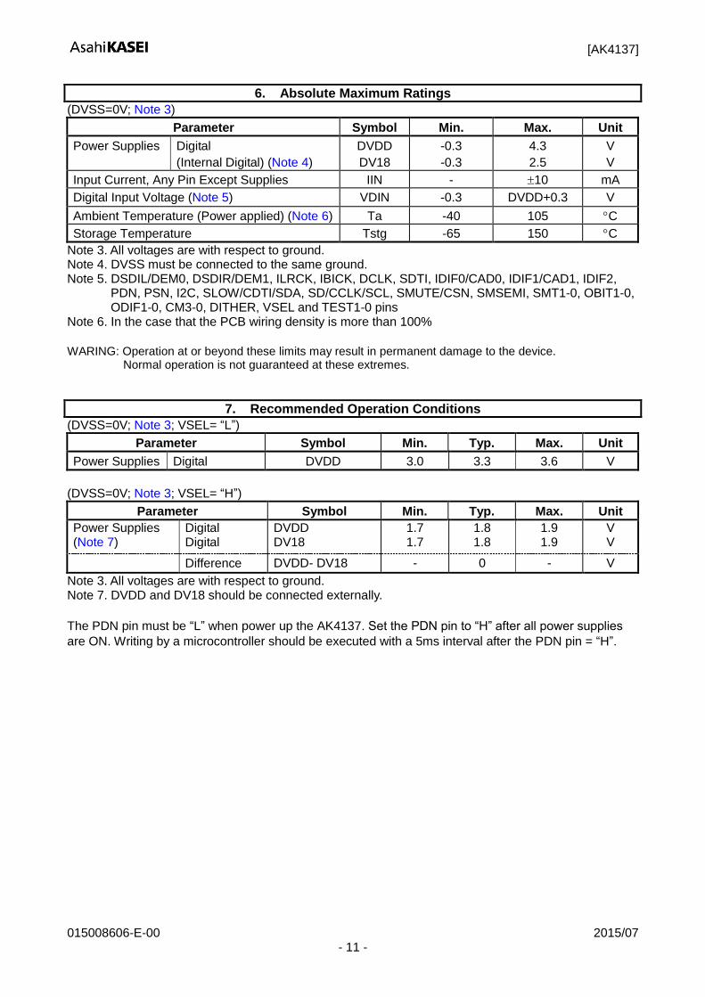
6. Absolute Maximum Ratings
(DVSS=0V; Note 3)
Parameter Symbol Min. Max. Unit
Power Supplies Digital
(Internal Digital) (Note 4)
DVDD
DV18
-0.3
-0.3
4.3
2.5
V
V
Input Current, Any Pin Except Supplies IIN - 10 mA
Digital Input Voltage (Note 5) VDIN -0.3 DVDD+0.3 V
Ambient Temperature (Power applied) (Note 6) Ta -40 105 C
Storage Temperature Tstg -65 150 C
Note 3. All voltages are with respect to ground. Note 4. DVSS must be connected to the same ground. Note 5. DSDIL/DEM0, DSDIR/DEM1, ILRCK, IBICK, DCLK, SDTI, IDIF0/CAD0, IDIF1/CAD1, IDIF2,
PDN, PSN, I2C, SLOW/CDTI/SDA, SD/CCLK/SCL, SMUTE/CSN, SMSEMI, SMT1-0, OBIT1-0, ODIF1-0, CM3-0, DITHER, VSEL and TEST1-0 pins
Note 6. In the case that the PCB wiring density is more than 100%
WARING: Operation at or beyond these limits may result in permanent damage to the device.
Normal operation is not guaranteed at these extremes.
7. Recommended Operation Conditions
(DVSS=0V; Note 3; VSEL= “L”)
Parameter Symbol Min. Typ. Max. Unit
Power Supplies Digital DVDD 3.0 3.3 3.6 V
(DVSS=0V; Note 3; VSEL= “H”)
Parameter Symbol Min. Typ. Max. Unit
Power Supplies (Note 7)
Digital Digital
DVDD DV18
1.7 1.7
1.8 1.8
1.9 1.9
V V
Difference DVDD- DV18 - 0 - V
Note 3. All voltages are with respect to ground. Note 7. DVDD and DV18 should be connected externally.
The PDN pin must be “L” when power up the AK4137. Set the PDN pin to “H” after all power supplies
are ON. Writing by a microcontroller should be executed with a 5ms interval after the PDN pin = “H”.
[AK4137]
015008606-E-00 2015/07 - 12 -
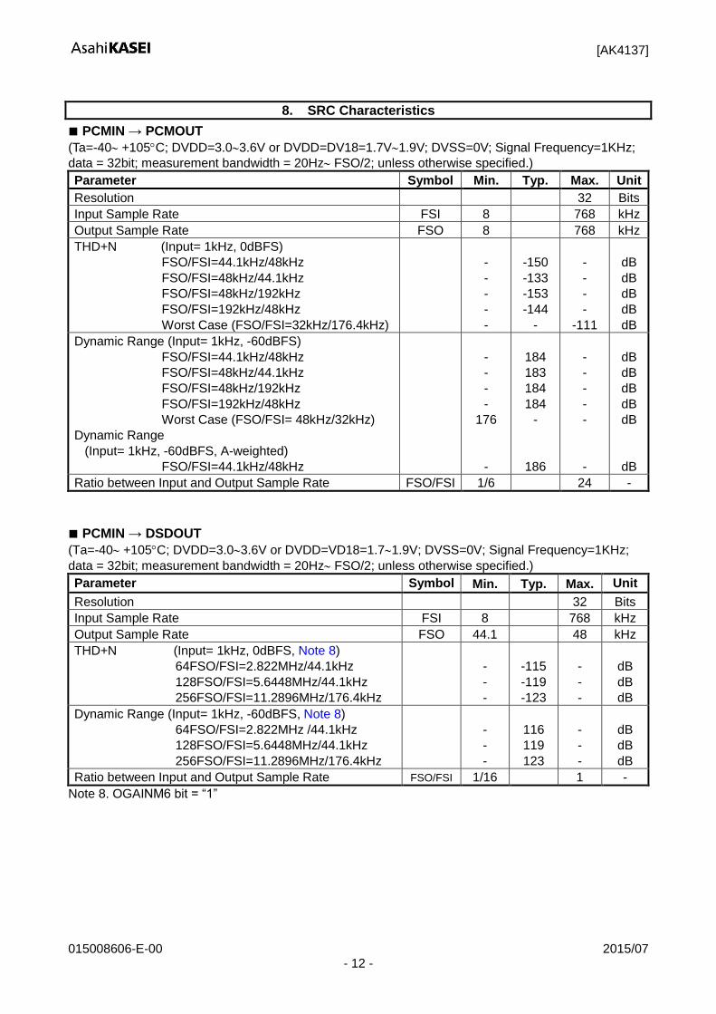
8. SRC Characteristics
PCMIN → PCMOUT
(Ta=-40 +105C; DVDD=3.03.6V or DVDD=DV18=1.7V1.9V; DVSS=0V; Signal Frequency=1KHz;
data = 32bit; measurement bandwidth = 20Hz FSO/2; unless otherwise specified.)
Parameter Symbol Min. Typ. Max. Unit
Resolution 32 Bits
Input Sample Rate FSI 8 768 kHz
Output Sample Rate FSO 8 768 kHz
THD+N (Input= 1kHz, 0dBFS)
FSO/FSI=44.1kHz/48kHz
FSO/FSI=48kHz/44.1kHz
FSO/FSI=48kHz/192kHz
FSO/FSI=192kHz/48kHz
Worst Case (FSO/FSI=32kHz/176.4kHz)
-
-
-
-
-
-150
-133
-153
-144
-
-
-
-
-
-111
dB
dB
dB
dB
dB
Dynamic Range (Input= 1kHz, -60dBFS)
FSO/FSI=44.1kHz/48kHz
FSO/FSI=48kHz/44.1kHz
FSO/FSI=48kHz/192kHz
FSO/FSI=192kHz/48kHz
Worst Case (FSO/FSI= 48kHz/32kHz)
Dynamic Range
(Input= 1kHz, -60dBFS, A-weighted)
FSO/FSI=44.1kHz/48kHz
-
-
-
-
176
-
184
183
184
184
-
186
-
-
-
-
-
-
dB
dB
dB
dB
dB
dB
Ratio between Input and Output Sample Rate FSO/FSI 1/6 24 -
PCMIN → DSDOUT
(Ta=-40 +105C; DVDD=3.03.6V or DVDD=VD18=1.71.9V; DVSS=0V; Signal Frequency=1KHz;
data = 32bit; measurement bandwidth = 20Hz FSO/2; unless otherwise specified.)
Parameter Symbol Min. Typ. Max. Unit
Resolution 32 Bits
Input Sample Rate FSI 8 768 kHz
Output Sample Rate FSO 44.1 48 kHz
THD+N (Input= 1kHz, 0dBFS, Note 8)
64FSO/FSI=2.822MHz/44.1kHz
128FSO/FSI=5.6448MHz/44.1kHz
256FSO/FSI=11.2896MHz/176.4kHz
-
-
-
-115
-119
-123
-
-
-
dB
dB
dB
Dynamic Range (Input= 1kHz, -60dBFS, Note 8)
64FSO/FSI=2.822MHz /44.1kHz
128FSO/FSI=5.6448MHz/44.1kHz
256FSO/FSI=11.2896MHz/176.4kHz
-
-
-
116
119
123
-
-
-
dB
dB
dB
Ratio between Input and Output Sample Rate FSO/FSI 1/16 1 -
Note 8. OGAINM6 bit = “1”
[AK4137]
015008606-E-00 2015/07 - 13 -
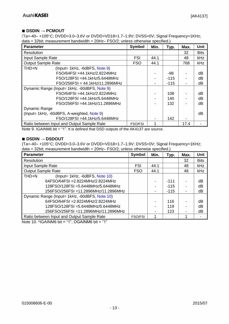
DSDIN → PCMOUT
(Ta=-40 +105C; DVDD=3.03.6V or DVDD=VD18=1.71.9V; DVSS=0V; Signal Frequency=1KHz;
data = 32bit; measurement bandwidth = 20Hz FSO/2; unless otherwise specified.)
Parameter Symbol Min. Typ. Max. Unit
Resolution 32 Bits
Input Sample Rate FSI 44.1 48 kHz
Output Sample Rate FSO 44.1 768 kHz
THD+N (Input= 1kHz, -6dBFS, Note 9)
FSO/64FSI =44.1kHz/2.8224MHz
FSO/128FSI =44.1kHz/5.6448MHz
FSO/256FSI = 44.1kHz/11.2896MHz
-
-
-
-98
-115
-115
-
-
-
dB
dB
dB
Dynamic Range (Input= 1kHz, -60dBFS, Note 9)
FSO/64FSI =44.1kHz/2.8224MHz
FSO/128FSI =44.1kHz/5.6448MHz
FSO/256FSI =44.1kHz/11.2896MHz
Dynamic Range
(Input= 1kHz, -60dBFS, A-weighted, Note 9)
FSO/128FSI =44.1kHz/5.6448MHz
-
-
-
-
108
140
132
142
-
-
-
-
dB
dB
dB
dB
Ratio between Input and Output Sample Rate FSO/FSI 1 17.4 -
Note 9. IGAINM6 bit = “1”. It is defined that DSD outputs of the AK4137 are source.
DSDIN → DSDOUT
(Ta=-40 +105C; DVDD=3.03.6V or DVDD=VD18=1.71.9V; DVSS=0V; Signal Frequency=1KHz;
data = 32bit; measurement bandwidth = 20Hz FSO/2; unless otherwise specified.)
Parameter Symbol Min. Typ. Max. Unit
Resolution 32 Bits
Input Sample Rate FSI 44.1 48 kHz
Output Sample Rate FSO 44.1 48 kHz
THD+N (Input= 1kHz, -6dBFS, Note 10)
64FSO/64FSI =2.8224MHz/2.8224MHz
128FSO/128FSI =5.6448MHz/5.6448MHz
256FSO/256FSI =11.2896MHz/11.2896MHz
-
-
-
-111
-115
-115
-
-
-
dB
dB
dB
Dynamic Range (Input= 1kHz, -60dBFS, Note 10)
64FSO/64FSI =2.8224MHz/2.8224MHz
128FSO/128FSI =5.6448MHz/5.6448MHz
256FSO/256FSI =11.2896MHz/11.2896MHz
-
-
-
116
119
123
-
-
-
dB
dB
dB
Ratio between Input and Output Sample Rate FSO/FSI 1 1 -
Note 10. *IGAINM6 bit = “1”, OGAINM6 bit = “1”
[AK4137]
015008606-E-00 2015/07 - 14 -
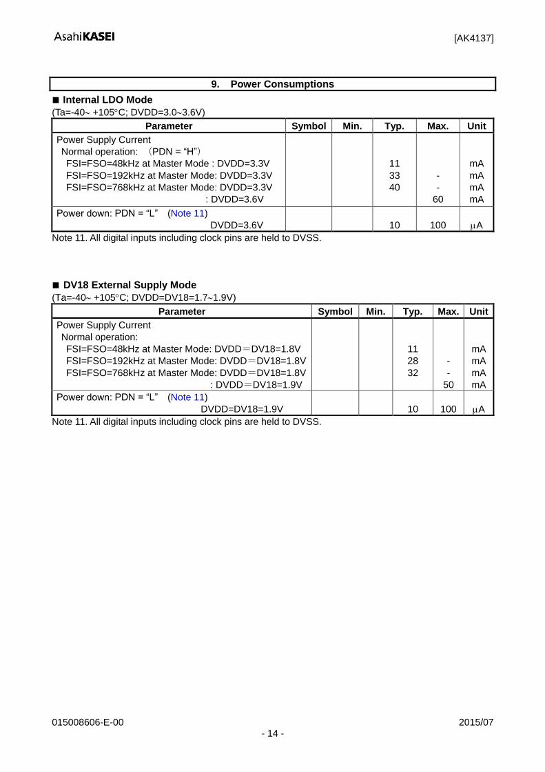
9. Power Consumptions
Internal LDO Mode
(Ta=-40 +105C; DVDD=3.03.6V)
Parameter Symbol Min. Typ. Max. Unit
Power Supply Current
Normal operation: (PDN = “H”)
FSI=FSO=48kHz at Master Mode : DVDD=3.3V
FSI=FSO=192kHz at Master Mode: DVDD=3.3V
FSI=FSO=768kHz at Master Mode: DVDD=3.3V
: DVDD=3.6V
11
33
40
-
-
60
mA
mA
mA
mA
Power down: PDN = “L” (Note 11)
DVDD=3.6V
10
100
A
Note 11. All digital inputs including clock pins are held to DVSS.
DV18 External Supply Mode
(Ta=-40 +105C; DVDD=DV18=1.71.9V)
Parameter Symbol Min. Typ. Max. Unit
Power Supply Current
Normal operation:
FSI=FSO=48kHz at Master Mode: DVDD=DV18=1.8V
FSI=FSO=192kHz at Master Mode: DVDD=DV18=1.8V
FSI=FSO=768kHz at Master Mode: DVDD=DV18=1.8V
: DVDD=DV18=1.9V
11
28
32
-
-
50
mA
mA
mA
mA
Power down: PDN = “L” (Note 11)
DVDD=DV18=1.9V
10
100
A
Note 11. All digital inputs including clock pins are held to DVSS.
[AK4137]
015008606-E-00 2015/07 - 15 -
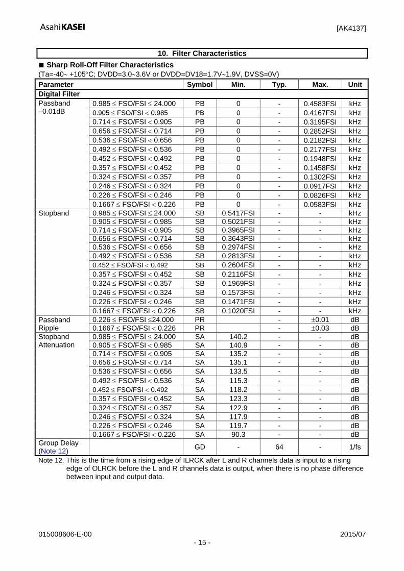
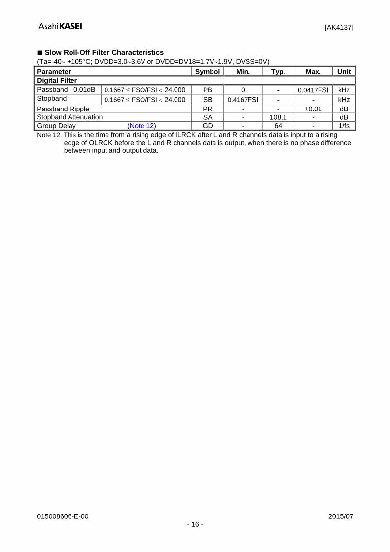
10. Filter Characteristics
Sharp Roll-Off Filter Characteristics
(Ta=-40 +105C; DVDD=3.03.6V or DVDD=DV18=1.7V1.9V, DVSS=0V)
Parameter Symbol Min. Typ. Max. Unit
Digital Filter
Passband 0.01dB
0.985 FSO/FSI 24.000 PB 0 - 0.4583FSI kHz
0.905 FSO/FSI 0.985 PB 0 - 0.4167FSI kHz
0.714 FSO/FSI 0.905 PB 0 - 0.3195FSI kHz
0.656 FSO/FSI 0.714 PB 0 - 0.2852FSI kHz
0.536 FSO/FSI 0.656 PB 0 - 0.2182FSI kHz
0.492 FSO/FSI 0.536 PB 0 - 0.2177FSI kHz
0.452 FSO/FSI 0.492 PB 0 - 0.1948FSI kHz
0.357 FSO/FSI 0.452 PB 0 - 0.1458FSI kHz
0.324 FSO/FSI 0.357 PB 0 - 0.1302FSI kHz
0.246 FSO/FSI 0.324 PB 0 - 0.0917FSI kHz
0.226 FSO/FSI 0.246 PB 0 - 0.0826FSI kHz
0.1667 FSO/FSI 0.226 PB 0 - 0.0583FSI kHz
Stopband 0.985 FSO/FSI 24.000 SB 0.5417FSI - - kHz
0.905 FSO/FSI 0.985 SB 0.5021FSI - - kHz
0.714 FSO/FSI 0.905 SB 0.3965FSI - - kHz
0.656 FSO/FSI 0.714 SB 0.3643FSI - - kHz
0.536 FSO/FSI 0.656 SB 0.2974FSI - - kHz
0.492 FSO/FSI 0.536 SB 0.2813FSI - - kHz
0.452 FSO/FSI 0.492 SB 0.2604FSI - - kHz
0.357 FSO/FSI 0.452 SB 0.2116FSI - - kHz
0.324 FSO/FSI 0.357 SB 0.1969FSI - - kHz
0.246 FSO/FSI 0.324 SB 0.1573FSI - - kHz
0.226 FSO/FSI 0.246 SB 0.1471FSI - - kHz
0.1667 FSO/FSI 0.226 SB 0.1020FSI - - kHz
Passband Ripple
0.226 FSO/FSI 24.000 PR - 0.01 dB
0.1667 FSO/FSI 0.226 PR - 0.03 dB
Stopband Attenuation
0.985 FSO/FSI 24.000 SA 140.2 - - dB
0.905 FSO/FSI 0.985 SA 140.9 - - dB
0.714 FSO/FSI 0.905 SA 135.2 - - dB
0.656 FSO/FSI 0.714 SA 135.1 - - dB
0.536 FSO/FSI 0.656 SA 133.5 - - dB
0.492 FSO/FSI 0.536 SA 115.3 - - dB
0.452 FSO/FSI 0.492 SA 118.2 - - dB
0.357 FSO/FSI 0.452 SA 123.3 - - dB
0.324 FSO/FSI 0.357 SA 122.9 - - dB
0.246 FSO/FSI 0.324 SA 117.9 - - dB
0.226 FSO/FSI 0.246 SA 119.7 - - dB
0.1667 FSO/FSI 0.226 SA 90.3 - - dB
Group Delay (Note 12)
GD - 64 - 1/fs
Note 12. This is the time from a rising edge of ILRCK after L and R channels data is input to a rising edge of OLRCK before the L and R channels data is output, when there is no phase difference between input and output data.
[AK4137]
015008606-E-00 2015/07 - 16 -
Slow Roll-Off Filter Characteristics
(Ta=-40 +105C; DVDD=3.03.6V or DVDD=DV18=1.7V1.9V, DVSS=0V)
Parameter Symbol Min. Typ. Max. Unit
Digital Filter
Passband 0.01dB 0.1667 FSO/FSI 24.000 PB 0 - 0.0417FSI kHz
Stopband 0.1667 FSO/FSI 24.000 SB 0.4167FSI - - kHz
Passband Ripple PR - - 0.01 dB
Stopband Attenuation SA - 108.1 - dB
Group Delay (Note 12) GD - 64 - 1/fs
Note 12. This is the time from a rising edge of ILRCK after L and R channels data is input to a rising edge of OLRCK before the L and R channels data is output, when there is no phase difference between input and output data.
[AK4137]
015008606-E-00 2015/07 - 17 -
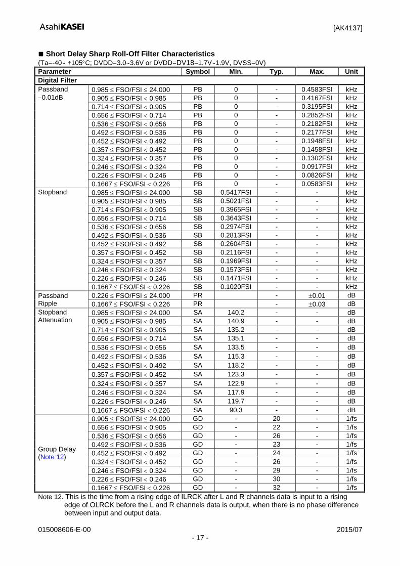
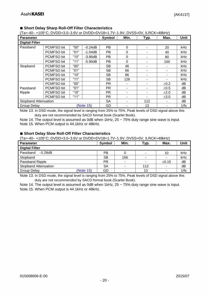
Short Delay Sharp Roll-Off Filter Characteristics
(Ta=-40 +105C; DVDD=3.03.6V or DVDD=DV18=1.7V1.9V, DVSS=0V)
Parameter Symbol Min. Typ. Max. Unit
Digital Filter
Passband
0.01dB 0.985 FSO/FSI 24.000 PB 0 - 0.4583FSI kHz
0.905 FSO/FSI 0.985 PB 0 - 0.4167FSI kHz
0.714 FSO/FSI 0.905 PB 0 - 0.3195FSI kHz
0.656 FSO/FSI 0.714 PB 0 - 0.2852FSI kHz
0.536 FSO/FSI 0.656 PB 0 - 0.2182FSI kHz
0.492 FSO/FSI 0.536 PB 0 - 0.2177FSI kHz
0.452 FSO/FSI 0.492 PB 0 - 0.1948FSI kHz
0.357 FSO/FSI 0.452 PB 0 - 0.1458FSI kHz
0.324 FSO/FSI 0.357 PB 0 - 0.1302FSI kHz
0.246 FSO/FSI 0.324 PB 0 - 0.0917FSI kHz
0.226 FSO/FSI 0.246 PB 0 - 0.0826FSI kHz
0.1667 FSO/FSI 0.226 PB 0 - 0.0583FSI kHz
Stopband 0.985 FSO/FSI 24.000 SB 0.5417FSI - - kHz
0.905 FSO/FSI 0.985 SB 0.5021FSI - - kHz
0.714 FSO/FSI 0.905 SB 0.3965FSI - - kHz
0.656 FSO/FSI 0.714 SB 0.3643FSI - - kHz
0.536 FSO/FSI 0.656 SB 0.2974FSI - - kHz
0.492 FSO/FSI 0.536 SB 0.2813FSI - - kHz
0.452 FSO/FSI 0.492 SB 0.2604FSI - - kHz
0.357 FSO/FSI 0.452 SB 0.2116FSI - - kHz
0.324 FSO/FSI 0.357 SB 0.1969FSI - - kHz
0.246 FSO/FSI 0.324 SB 0.1573FSI - - kHz
0.226 FSO/FSI 0.246 SB 0.1471FSI - - kHz
0.1667 FSO/FSI 0.226 SB 0.1020FSI - - kHz
Passband Ripple
0.226 FSO/FSI 24.000 PR - 0.01 dB
0.1667 FSO/FSI 0.226 PR - 0.03 dB
Stopband Attenuation
0.985 FSO/FSI 24.000 SA 140.2 - - dB
0.905 FSO/FSI 0.985 SA 140.9 - - dB
0.714 FSO/FSI 0.905 SA 135.2 - - dB
0.656 FSO/FSI 0.714 SA 135.1 - - dB
0.536 FSO/FSI 0.656 SA 133.5 - - dB
0.492 FSO/FSI 0.536 SA 115.3 - - dB
0.452 FSO/FSI 0.492 SA 118.2 - - dB
0.357 FSO/FSI 0.452 SA 123.3 - - dB
0.324 FSO/FSI 0.357 SA 122.9 - - dB
0.246 FSO/FSI 0.324 SA 117.9 - - dB
0.226 FSO/FSI 0.246 SA 119.7 - - dB
0.1667 FSO/FSI 0.226 SA 90.3 - - dB
Group Delay (Note 12)
0.905 FSO/FSI 24.000 GD - 20 - 1/fs
0.656 FSO/FSI 0.905 GD - 22 - 1/fs
0.536 FSO/FSI 0.656 GD - 26 - 1/fs
0.492 FSO/FSI 0.536 GD - 23 - 1/fs
0.452 FSO/FSI 0.492 GD - 24 - 1/fs
0.324 FSO/FSI 0.452 GD - 26 - 1/fs
0.246 FSO/FSI 0.324 GD - 29 - 1/fs
0.226 FSO/FSI 0.246 GD - 30 - 1/fs
0.1667 FSO/FSI 0.226 GD - 32 - 1/fs
Note 12. This is the time from a rising edge of ILRCK after L and R channels data is input to a rising edge of OLRCK before the L and R channels data is output, when there is no phase difference between input and output data.
[AK4137]
015008606-E-00 2015/07 - 18 -
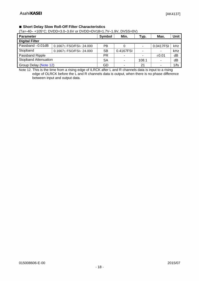
Short Delay Slow Roll-Off Filter Characteristics
(Ta=-40 +105C; DVDD=3.03.6V or DVDD=DV18=1.7V1.9V, DVSS=0V)
Parameter Symbol Min. Typ. Max. Unit
Digital Filter
Passband 0.01dB 0.1667 FSO/FSI 24.000 PB 0 - 0.0417FSI kHz
Stopband 0.1667 FSO/FSI 24.000 SB 0.4167FSI - - kHz
Passband Ripple PR - - 0.01 dB
Stopband Attenuation SA - 108.1 - dB
Group Delay (Note 12) GD - 21 - 1/fs
Note 12. This is the time from a rising edge of ILRCK after L and R channels data is input to a rising edge of OLRCK before the L and R channels data is output, when there is no phase difference between input and output data.
[AK4137]
015008606-E-00 2015/07 - 19 -
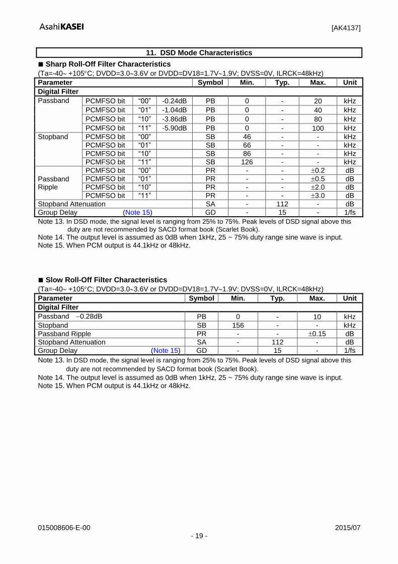
11. DSD Mode Characteristics
Sharp Roll-Off Filter Characteristics
(Ta=-40 +105C; DVDD=3.03.6V or DVDD=DV18=1.7V1.9V; DVSS=0V, ILRCK=48kHz)
Parameter Symbol Min. Typ. Max. Unit
Digital Filter
Passband
PCMFSO bit “00” -0.24dB PB 0 - 20 kHz
PCMFSO bit “01” -1.04dB PB 0 - 40 kHz
PCMFSO bit “10” -3.86dB PB 0 - 80 kHz
PCMFSO bit “11” -5.90dB PB 0 - 100 kHz
Stopband PCMFSO bit “00” SB 46 - - kHz
PCMFSO bit “01” SB 66 - - kHz
PCMFSO bit “10” SB 86 - - kHz
PCMFSO bit “11” SB 126 - - kHz
Passband Ripple
PCMFSO bit “00” PR - - 0.2 dB
PCMFSO bit “01” PR - - 0.5 dB
PCMFSO bit “10” PR - - 2.0 dB
PCMFSO bit “11” PR - - 3.0 dB
Stopband Attenuation SA - 112 - dB
Group Delay (Note 15) GD - 15 - 1/fs
Note 13. In DSD mode, the signal level is ranging from 25% to 75%. Peak levels of DSD signal above this
duty are not recommended by SACD format book (Scarlet Book).
Note 14. The output level is assumed as 0dB when 1kHz, 25 ~ 75% duty range sine wave is input. Note 15. When PCM output is 44.1kHz or 48kHz.
Slow Roll-Off Filter Characteristics
(Ta=-40 +105C; DVDD=3.03.6V or DVDD=DV18=1.7V1.9V; DVSS=0V, ILRCK=48kHz)
Parameter Symbol Min. Typ. Max. Unit
Digital Filter
Passband 0.28dB PB 0 - 10 kHz
Stopband SB 156 - - kHz
Passband Ripple PR - - 0.15 dB
Stopband Attenuation SA - 112 - dB
Group Delay (Note 15) GD - 15 - 1/fs
Note 13. In DSD mode, the signal level is ranging from 25% to 75%. Peak levels of DSD signal above this
duty are not recommended by SACD format book (Scarlet Book).
Note 14. The output level is assumed as 0dB when 1kHz, 25 ~ 75% duty range sine wave is input. Note 15. When PCM output is 44.1kHz or 48kHz.
[AK4137]
015008606-E-00 2015/07 - 20 -
Short Delay Sharp Roll-Off Filter Characteristics
(Ta=-40 +105C; DVDD=3.03.6V or DVDD=DV18=1.7V1.9V; DVSS=0V, ILRCK=48kHz)
Parameter Symbol Min. Typ. Max. Unit
Digital Filter
Passband
PCMFSO bit “00” -0.24dB PB 0 - 20 kHz
PCMFSO bit “01” -1.04dB PB 0 - 40 kHz
PCMFSO bit “10” -3.86dB PB 0 - 80 kHz
PCMFSO bit “11” -5.90dB PB 0 - 100 kHz
Stopband PCMFSO bit “00” SB 46 - - kHz
PCMFSO bit “01” SB 66 - - kHz
PCMFSO bit “10” SB 86 - - kHz
PCMFSO bit “11” SB 126 - - kHz
Passband
Ripple
PCMFSO bit “00” PR - - 0.2 dB
PCMFSO bit “01” PR - - 0.5 dB
PCMFSO bit “10” PR - - 2.0 dB
PCMFSO bit “11” PR - - 3.0 dB
Stopband Attenuation SA - 112 - dB
Group Delay (Note 15) GD - 13 - 1/fs
Note 13. In DSD mode, the signal level is ranging from 25% to 75%. Peak levels of DSD signal above this
duty are not recommended by SACD format book (Scarlet Book).
Note 14. The output level is assumed as 0dB when 1kHz, 25 ~ 75% duty range sine wave is input. Note 15. When PCM output is 44.1kHz or 48kHz.
Short Delay Slow Roll-Off Filter Characteristics
(Ta=-40 +105C; DVDD=3.03.6V or DVDD=DV18=1.7V1.9V; DVSS=0V, ILRCK=48kHz)
Parameter Symbol Min. Typ. Max. Unit
Digital Filter
Passband 0.28dB PB 0 - 10 kHz
Stopband SB 156 - - kHz
Passband Ripple PR - - 0.15 dB
Stopband Attenuation SA - 112 - dB
Group Delay (Note 15) GD - 13 - 1/fs
Note 13. In DSD mode, the signal level is ranging from 25% to 75%. Peak levels of DSD signal above this
duty are not recommended by SACD format book (Scarlet Book).
Note 14. The output level is assumed as 0dB when 1kHz, 25 ~ 75% duty range sine wave is input.
Note 15. When PCM output is 44.1kHz or 48kHz.
[AK4137]
015008606-E-00 2015/07 - 21 -
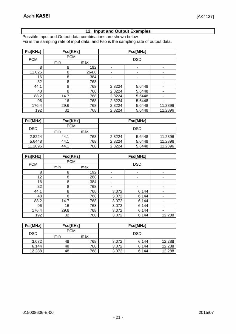
12. Input and Output Examples
Possible Input and Output data combinations are shown below. Fsi is the sampling rate of input data, and Fso is the sampling rate of output data.
Fsi[KHz] Fso[KHz] Fso[MHz]
PCM PCM
DSD min max
8 8 192 - - -
11.025 8 264.6 - - -
16 8 384 - - -
32 8 768 - - -
44.1 8 768 2.8224 5.6448 -
48 8 768 2.8224 5.6448 -
88.2 14.7 768 2.8224 5.6448 -
96 16 768 2.8224 5.6448 -
176.4 29.6 768 2.8224 5.6448 11.2896
192 32 768 2.8224 5.6448 11.2896
Fsi[MHz] Fso[KHz] Fso[MHz]
DSD PCM
DSD min max
2.8224 44.1 768 2.8224 5.6448 11.2896
5.6448 44.1 768 2.8224 5.6448 11.2896
11.2896 44.1 768 2.8224 5.6448 11.2896
Fsi[KHz] Fso[KHz] Fso[MHz]
PCM PCM
DSD min max
8 8 192 - - -
12 8 288 - - -
16 8 384 - - -
32 8 768 - - -
44.1 8 768 3.072 6.144 -
48 8 768 3.072 6.144 -
88.2 14.7 768 3.072 6.144 -
96 16 768 3.072 6.144 -
176.4 29.6 768 3.072 6.144 -
192 32 768 3.072 6.144 12.288
Fsi[MHz] Fso[KHz] Fso[MHz]
DSD PCM
DSD min max
3.072 48 768 3.072 6.144 12.288
6.144 48 768 3.072 6.144 12.288
12.288 48 768 3.072 6.144 12.288
[AK4137]
015008606-E-00 2015/07 - 22 -
With combinations shown below, in case down convert, THD+N will be degraded -80dB.
Fsi[KHz] Fso[KHz] Fso[MHz]
PCM PCM
DSD min max
384 64~384 768 2.8224 5.6448 11.2896
768 128~768 768 2.8224 5.6448 11.2896
Fsi[KHz] Fso[KHz] Fso[MHz]
PCM PCM
DSD min max
384 64~384 768 3.072 6.144 12.288
768 128~768 768 3.072 6.144 12.288
[AK4137]
015008606-E-00 2015/07 - 23 -
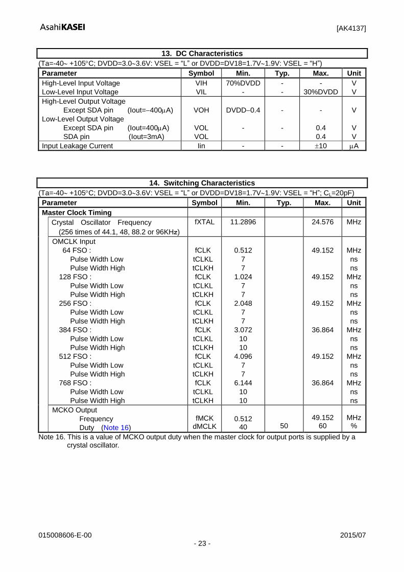
13. DC Characteristics
(Ta=-40 +105C; DVDD=3.03.6V: VSEL = “L” or DVDD=DV18=1.7V1.9V: VSEL = “H”)
Parameter Symbol Min. Typ. Max. Unit
High-Level Input Voltage
Low-Level Input Voltage
VIH
VIL
70%DVDD
-
-
-
-
30%DVDD
V
V
High-Level Output Voltage
Except SDA pin (Iout=400A)
Low-Level Output Voltage
Except SDA pin (Iout=400A)
SDA pin (Iout=3mA)
VOH
VOL
VOL
DVDD0.4
-
-
-
-
0.4
0.4
V
V
V
Input Leakage Current Iin - - 10 A
14. Switching Characteristics
(Ta=-40 +105C; DVDD=3.03.6V: VSEL = “L” or DVDD=DV18=1.7V1.9V: VSEL = “H”; CL=20pF)
Parameter Symbol Min. Typ. Max. Unit
Master Clock Timing
Crystal Oscillator Frequency
(256 times of 44.1, 48, 88.2 or 96KHz)
fXTAL 11.2896 24.576 MHz
OMCLK Input
64 FSO :
Pulse Width Low
Pulse Width High
128 FSO :
Pulse Width Low
Pulse Width High
256 FSO :
Pulse Width Low
Pulse Width High
384 FSO :
Pulse Width Low
Pulse Width High
512 FSO :
Pulse Width Low
Pulse Width High
768 FSO :
Pulse Width Low
Pulse Width High
fCLK
tCLKL
tCLKH
fCLK
tCLKL
tCLKH
fCLK
tCLKL
tCLKH
fCLK
tCLKL
tCLKH
fCLK
tCLKL
tCLKH
fCLK
tCLKL
tCLKH
0.512
7
7
1.024
7
7
2.048
7
7
3.072
10
10
4.096
7
7
6.144
10
10
49.152
49.152
49.152
36.864
49.152
36.864
MHz
ns
ns
MHz
ns
ns
MHz
ns
ns
MHz
ns
ns
MHz
ns
ns
MHz
ns
ns
MCKO Output
Frequency
Duty (Note 16)
fMCK
dMCLK
0.512 40
50
49.152
60
MHz
%
Note 16. This is a value of MCKO output duty when the master clock for output ports is supplied by a crystal oscillator.
[AK4137]
015008606-E-00 2015/07 - 24 -
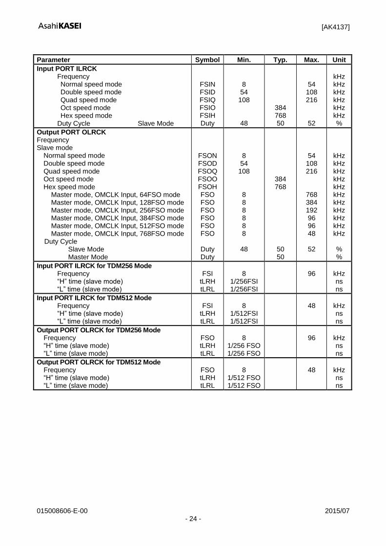
Parameter Symbol Min. Typ. Max. Unit
Input PORT ILRCK Frequency
Normal speed mode Double speed mode Quad speed mode Oct speed mode Hex speed mode
Duty Cycle Slave Mode
FSIN FSID FSIQ FSIO FSIH Duty
8 54
108
48
384 768 50
54 108 216
52
kHz kHz kHz kHz kHz kHz %
Output PORT OLRCK Frequency Slave mode Normal speed mode Double speed mode Quad speed mode Oct speed mode Hex speed mode
Master mode, OMCLK Input, 64FSO mode Master mode, OMCLK Input, 128FSO mode Master mode, OMCLK Input, 256FSO mode Master mode, OMCLK Input, 384FSO mode Master mode, OMCLK Input, 512FSO mode Master mode, OMCLK Input, 768FSO mode
Duty Cycle Slave Mode Master Mode
FSON FSOD FSOQ FSOO FSOH FSO FSO FSO FSO FSO FSO
Duty Duty
8 54
108 8 8 8 8 8 8
48
384 768
50 50
54 108 216
768 384 192 96 96 48
52
kHz kHz kHz kHz kHz kHz kHz kHz kHz kHz kHz
% %
Input PORT ILRCK for TDM256 Mode Frequency “H” time (slave mode) “L” time (slave mode)
FSI
tLRH tLRL
8
1/256FSI 1/256FSI
96
kHz ns ns
Input PORT ILRCK for TDM512 Mode Frequency “H” time (slave mode) “L” time (slave mode)
FSI
tLRH tLRL
8
1/512FSI 1/512FSI
48
kHz ns ns
Output PORT OLRCK for TDM256 Mode Frequency “H” time (slave mode) “L” time (slave mode)
FSO tLRH tLRL
8
1/256 FSO 1/256 FSO
96
kHz ns ns
Output PORT OLRCK for TDM512 Mode Frequency “H” time (slave mode) “L” time (slave mode)
FSO tLRH tLRL
8
1/512 FSO 1/512 FSO
48
kHz ns ns
[AK4137]
015008606-E-00 2015/07 - 25 -
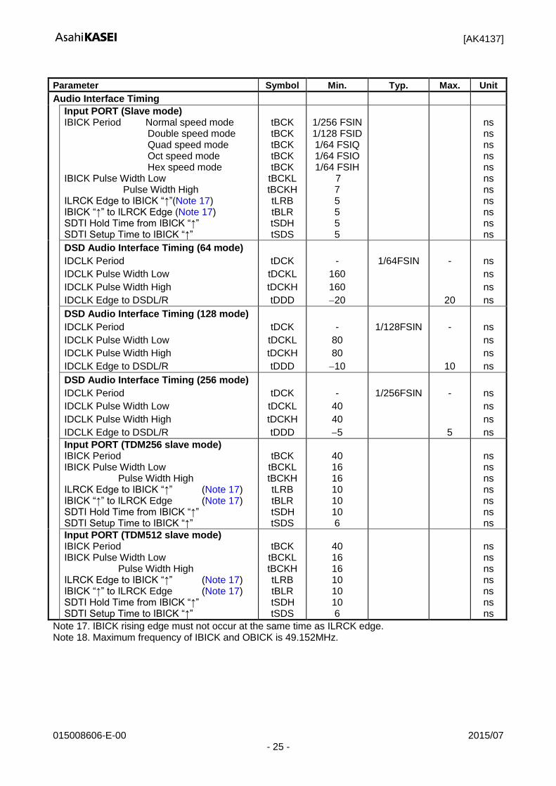
Parameter Symbol Min. Typ. Max. Unit
Audio Interface Timing
Input PORT (Slave mode) IBICK Period Normal speed mode Double speed mode Quad speed mode Oct speed mode Hex speed mode IBICK Pulse Width Low Pulse Width High ILRCK Edge to IBICK “↑”(Note 17) IBICK “↑” to ILRCK Edge (Note 17) SDTI Hold Time from IBICK “↑” SDTI Setup Time to IBICK “↑”
tBCK tBCK tBCK tBCK tBCK
tBCKL tBCKH tLRB tBLR tSDH tSDS
1/256 FSIN 1/128 FSID 1/64 FSIQ 1/64 FSIO 1/64 FSIH
7 7 5 5 5 5
ns ns ns ns ns ns ns ns ns ns ns
DSD Audio Interface Timing (64 mode)
IDCLK Period
IDCLK Pulse Width Low
IDCLK Pulse Width High
IDCLK Edge to DSDL/R
tDCK
tDCKL
tDCKH
tDDD
-
160
160
20
1/64FSIN
-
20
ns
ns
ns
ns
DSD Audio Interface Timing (128 mode)
IDCLK Period
IDCLK Pulse Width Low
IDCLK Pulse Width High
IDCLK Edge to DSDL/R
tDCK
tDCKL
tDCKH
tDDD
-
80
80
10
1/128FSIN
-
10
ns
ns
ns
ns
DSD Audio Interface Timing (256 mode)
IDCLK Period
IDCLK Pulse Width Low
IDCLK Pulse Width High
IDCLK Edge to DSDL/R
tDCK
tDCKL
tDCKH
tDDD
-
40
40
5
1/256FSIN
-
5
ns
ns
ns
ns
Input PORT (TDM256 slave mode) IBICK Period IBICK Pulse Width Low Pulse Width High ILRCK Edge to IBICK “↑” (Note 17) IBICK “↑” to ILRCK Edge (Note 17) SDTI Hold Time from IBICK “↑” SDTI Setup Time to IBICK “↑”
tBCK
tBCKL tBCKH tLRB tBLR tSDH tSDS
40 16 16 10 10 10 6
ns ns ns ns ns ns ns
Input PORT (TDM512 slave mode) IBICK Period IBICK Pulse Width Low Pulse Width High ILRCK Edge to IBICK “↑” (Note 17) IBICK “↑” to ILRCK Edge (Note 17) SDTI Hold Time from IBICK “↑” SDTI Setup Time to IBICK “↑”
tBCK
tBCKL tBCKH tLRB tBLR tSDH tSDS
40 16 16 10 10 10 6
ns ns ns ns ns ns ns
Note 17. IBICK rising edge must not occur at the same time as ILRCK edge. Note 18. Maximum frequency of IBICK and OBICK is 49.152MHz.
[AK4137]
015008606-E-00 2015/07 - 26 -
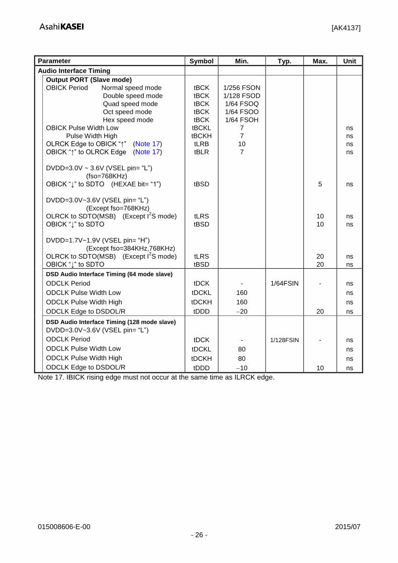
Parameter Symbol Min. Typ. Max. Unit
Audio Interface Timing
Output PORT (Slave mode)
OBICK Period Normal speed mode
Double speed mode
Quad speed mode
Oct speed mode
Hex speed mode
OBICK Pulse Width Low
Pulse Width High
OLRCK Edge to OBICK “↑” (Note 17)
OBICK “↑” to OLRCK Edge (Note 17)
DVDD=3.0V ~ 3.6V (VSEL pin= “L”)
(fso=768KHz)
OBICK “↓” to SDTO (HEXAE bit= “1”)
DVDD=3.0V~3.6V (VSEL pin= “L”)
(Except fso=768KHz)
OLRCK to SDTO(MSB) (Except I2S mode)
OBICK “↓” to SDTO
DVDD=1.7V~1.9V (VSEL pin= “H”)
(Except fso=384KHz,768KHz)
OLRCK to SDTO(MSB) (Except I2S mode)
OBICK “↓” to SDTO
tBCK
tBCK
tBCK
tBCK
tBCK
tBCKL
tBCKH
tLRB
tBLR
tBSD
tLRS
tBSD
tLRS
tBSD
1/256 FSON
1/128 FSOD
1/64 FSOQ
1/64 FSOO
1/64 FSOH
7
7
10
7
5
10
10
20
20
ns
ns
ns
ns
ns
ns
ns
ns
ns
DSD Audio Interface Timing (64 mode slave)
ODCLK Period
ODCLK Pulse Width Low
ODCLK Pulse Width High
ODCLK Edge to DSDOL/R
tDCK
tDCKL
tDCKH
tDDD
-
160
160
20
1/64FSIN
-
20
ns
ns
ns
ns
DSD Audio Interface Timing (128 mode slave)
DVDD=3.0V~3.6V (VSEL pin= “L”)
ODCLK Period
ODCLK Pulse Width Low
ODCLK Pulse Width High
ODCLK Edge to DSDOL/R
tDCK
tDCKL
tDCKH
tDDD
-
80
80
10
1/128FSIN
-
10
ns
ns
ns
ns
Note 17. IBICK rising edge must not occur at the same time as ILRCK edge.
[AK4137]
015008606-E-00 2015/07 - 27 -
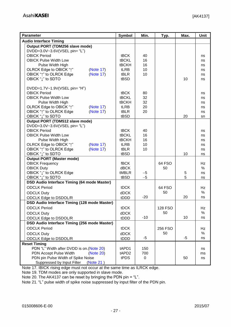
Parameter Symbol Min. Typ. Max. Unit
Audio Interface Timing
Output PORT (TDM256 slave mode)
DVDD=3.0V~3.6V(VSEL pin= “L”)
OBICK Period
OBICK Pulse Width Low
Pulse Width High
OLRCK Edge to OBICK “↑” (Note 17)
OBICK “↑” to OLRCK Edge (Note 17)
OBICK “↓” to SDTO
DVDD=1.7V~1.9V(VSEL pin= “H”)
OBICK Period
OBICK Pulse Width Low
Pulse Width High
OLRCK Edge to OBICK “↑” (Note 17)
OBICK “↑” to OLRCK Edge (Note 17)
OBICK “↓” to SDTO
tBCK
tBCKL
tBCKH
tLRB
tBLR
tBSD
tBCK
tBCKL
tBCKH
tLRB
tBLR
tBSD
40
16
16
10
10
80
32
32
20
20
10
20
ns
ns
ns
ns
ns
ns
ns
ns
ns
ns
ns
sn
Output PORT (TDM512 slave mode)
DVDD=3.0V~3.6V(VSEL pin= “L”)
OBICK Period
OBICK Pulse Width Low
Pulse Width High
OLRCK Edge to OBICK “↑” (Note 17)
OBICK “↑” to OLRCK Edge (Note 17)
OBICK “↓” to SDTO
tBCK
tBCKL
tBCKH
tLRB
tBLR
tBSD
40
16
16
10
10
10
ns
ns
ns
ns
ns
ns
Output PORT (Master mode)
OBICK Frequency
OBICK Duty
OBICK “↓” to OLRCK Edge
OBICK “↓” to SDTO
fBCK
dBCK
tMBLR
tBSD
5
5
64 FSO
50
5
5
Hz
%
ns
ns
DSD Audio Interface Timing (64 mode Master)
ODCLK Period
ODCLK Duty
ODCLK Edge to DSDOL/R
tDCK
dDCK
tDDD
-20
64 FSO
50
20
Hz
%
ns
DSD Audio Interface Timing (128 mode Master)
ODCLK Period
ODCLK Duty
ODCLK Edge to DSDOL/R
tDCK
dDCK
tDDD
-10
128 FSO
50
10
Hz
%
ns
DSD Audio Interface Timing (256 mode Master)
ODCLK Period
ODCLK Duty
ODCLK Edge to DSDOL/R
tDCK
dDCK
tDDD
-5
256 FSO
50
-5
Hz
%
ns
Reset Timing
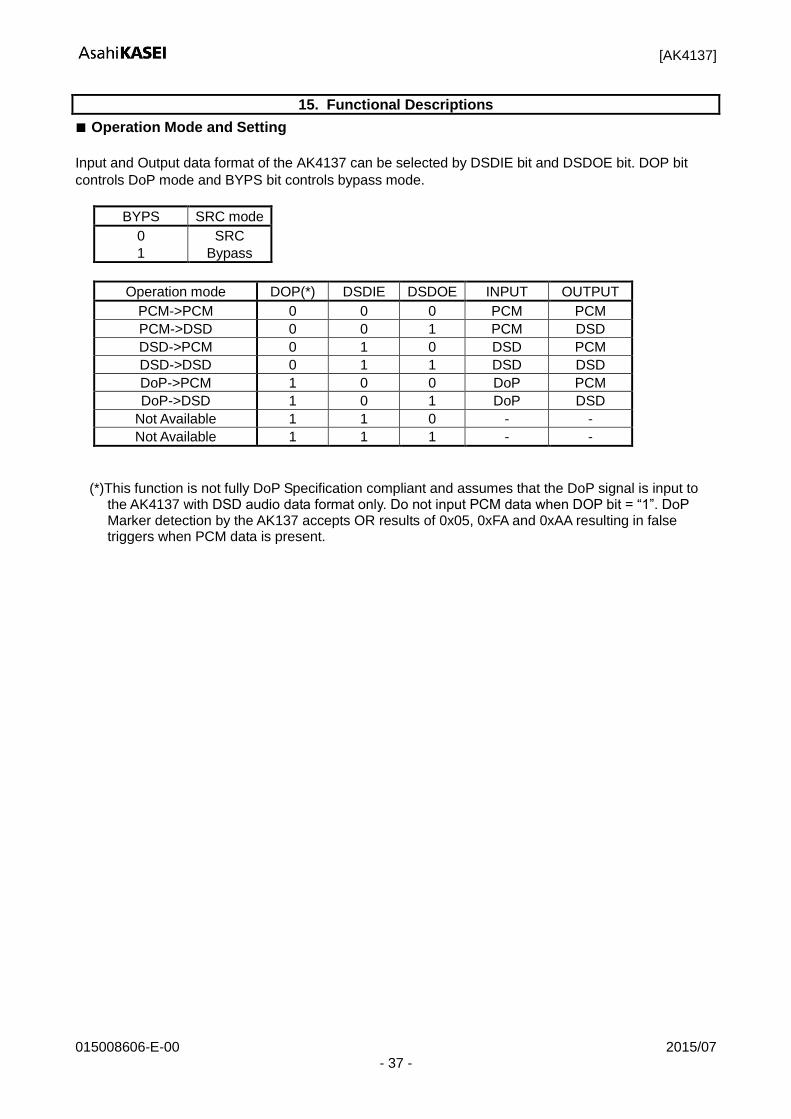
PDN “L” Width after DVDD is on.(Note 20)
PDN Accept Pulse Width (Note 20)
PDN pin Pulse Width of Spike Noise
Suppressed by Input Filter (Note 21 )
tAPD1
tAPD2
tPDS
150
700
0
50
ns
ms
ns
Note 17. IBICK rising edge must not occur at the same time as ILRCK edge. Note 19. TDM modes are only supported in slave mode. Note 20. The AK4137 can be reset by bringing the PDN pin = “L”.
Note 21. “L” pulse width of spike noise suppressed by input filter of the PDN pin.
[AK4137]
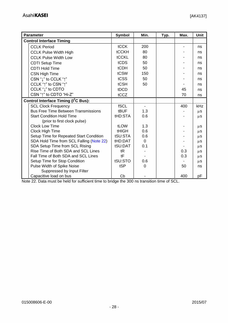
015008606-E-00 2015/07 - 28 -
Parameter Symbol Min. Typ. Max. Unit
Control Interface Timing
CCLK Period
CCLK Pulse Width High
CCLK Pulse Width Low
CDTI Setup Time
CDTI Hold Time
CSN High Time
CSN “↓” to CCLK “↑”
CCLK “↑” to CSN “↑”
CCLK “↓” to CDTO
CSN “↑” to CDTO “Hi-Z”
tCCK
tCCKH
tCCKL
tCDS
tCDH
tCSW
tCSS
tCSH
tDCD
tCCZ
200
80
80
50
50
150
50
50
-
-
-
-
-
-
-
-
45
70
ns
ns
ns
ns
ns
ns
ns
ns
ns
ns
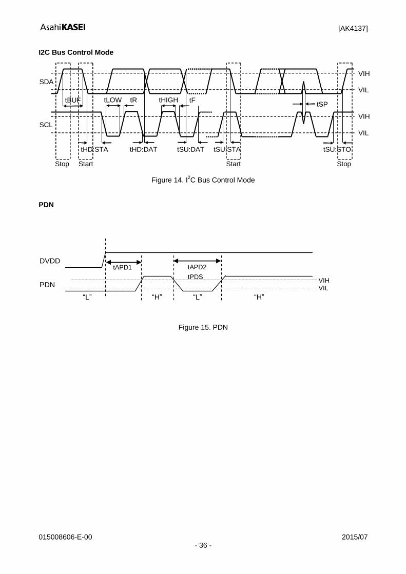
Control Interface Timing (I2C Bus):
SCL Clock Frequency
Bus Free Time Between Transmissions
Start Condition Hold Time
(prior to first clock pulse)
Clock Low Time
Clock High Time
Setup Time for Repeated Start Condition
SDA Hold Time from SCL Falling (Note 22)
SDA Setup Time from SCL Rising
Rise Time of Both SDA and SCL Lines
Fall Time of Both SDA and SCL Lines
Setup Time for Stop Condition
Pulse Width of Spike Noise
Suppressed by Input Filter
Capacitive load on bus
fSCL
tBUF
tHD:STA
tLOW
tHIGH
tSU:STA
tHD:DAT
tSU:DAT
tR
tF
tSU:STO
tSP
Cb
-
1.3
0.6
1.3
0.6
0.6
0
0.1
-
-
0.6
0
-
400
-
-
-
-
-
-
-
0.3
0.3
-
50
400
kHz
s
s
s
s
s
s
s
s
s
s
ns
pF
Note 22. Data must be held for sufficient time to bridge the 300 ns transition time of SCL.
[AK4137]
015008606-E-00 2015/07 - 29 -
Timing Diagrams
1/fCLK
tCLKL
VIH
tCLKH
XTI VIL
1/fCLK
tCLKL
VIH
tCLKH
OMCLK(I) VIL
dCLK=tCLKH(or fCKL)x fCLKx100
1/fMCK
tMCKL
50%DVDD
tMCKH
MCKO(O)
dMCK=tMCKH (or tMCKL) x fMCK X100
Figure 3. OMCLK, MCKO Clock Timing
[AK4137]
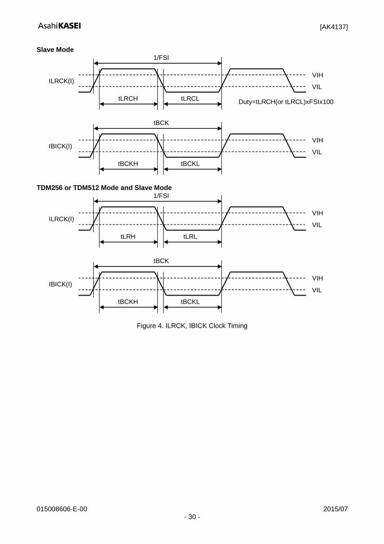
015008606-E-00 2015/07 - 30 -
Slave Mode 1/FSI
tLRCL
VIH
tLRCH
ILRCK(I) VIL
Duty=tLRCH(or tLRCL)xFSIx100
tBCK
tBCKL
VIH
tBCKH
IBICK(I) VIL
TDM256 or TDM512 Mode and Slave Mode
1/FSI
tLRL
VIH
tLRH
ILRCK(I) VIL
tBCK
tBCKL
VIH
tBCKH
IBICK(I) VIL
Figure 4. ILRCK, IBICK Clock Timing
[AK4137]
015008606-E-00 2015/07 - 31 -
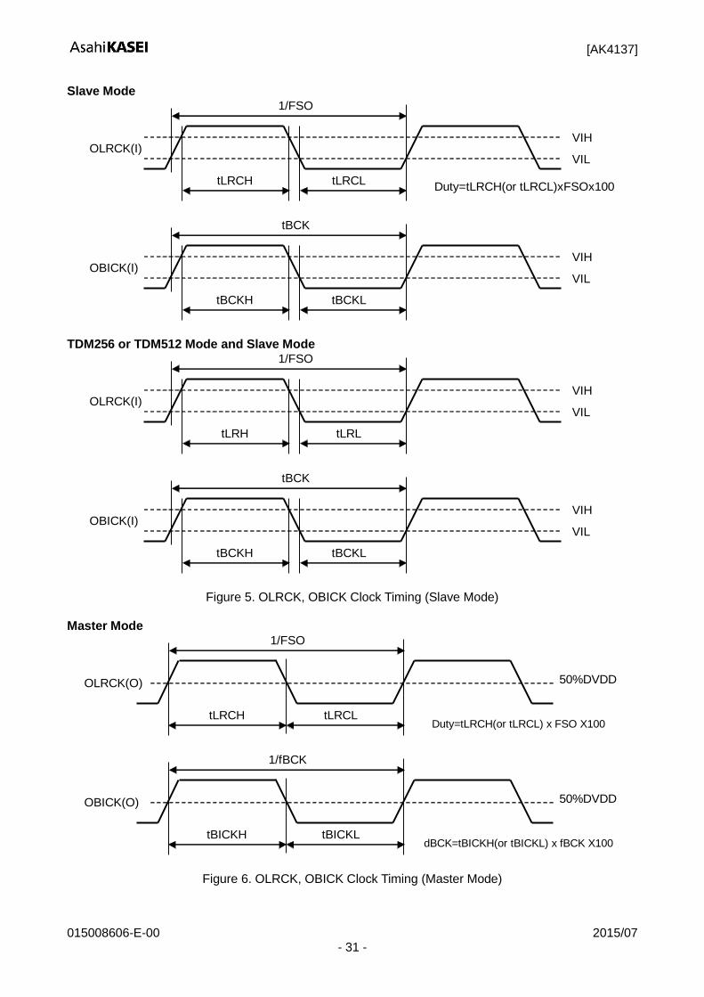
Slave Mode 1/FSO
tLRCL
VIH
tLRCH
OLRCK(I) VIL
Duty=tLRCH(or tLRCL)xFSOx100
tBCK
tBCKL
VIH
tBCKH
OBICK(I) VIL
TDM256 or TDM512 Mode and Slave Mode
1/FSO
tLRL
VIH
tLRH
OLRCK(I) VIL
tBCK
tBCKL
VIH
tBCKH
OBICK(I) VIL
Figure 5. OLRCK, OBICK Clock Timing (Slave Mode) Master Mode
1/FSO
tLRCL
50%DVDD
tLRCH
OLRCK(O)
Duty=tLRCH(or tLRCL) x FSO X100
1/fBCK
tBICKL
50%DVDD
tBICKH
OBICK(O)
dBCK=tBICKH(or tBICKL) x fBCK X100
Figure 6. OLRCK, OBICK Clock Timing (Master Mode)
[AK4137]
015008606-E-00 2015/07 - 32 -
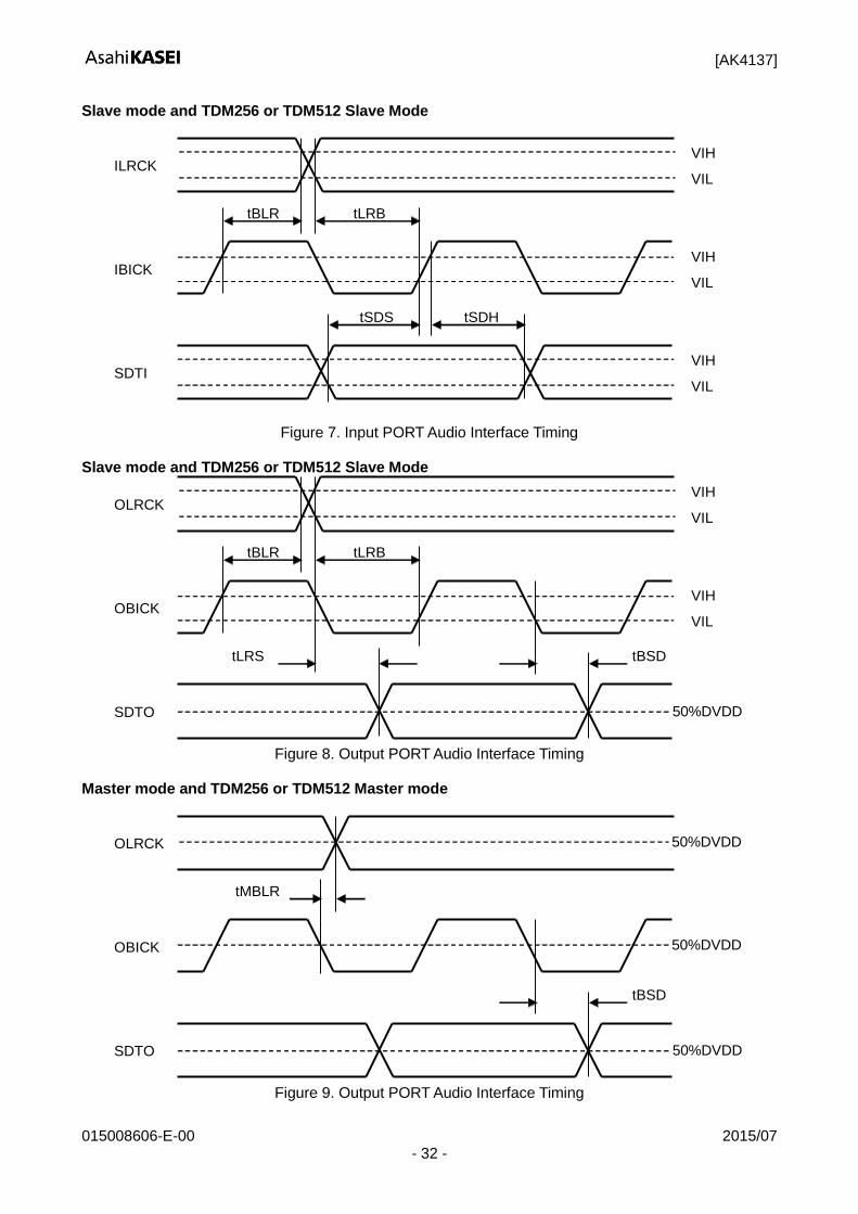
Slave mode and TDM256 or TDM512 Slave Mode
tLRB
ILRCK
VIH IBICK
VIL
tSDS
VIH SDTI
VIL
tSDH
VIH
VIL
tBLR
Figure 7. Input PORT Audio Interface Timing Slave mode and TDM256 or TDM512 Slave Mode
tLRB
OLRCK
VIH OBICK
VIL
tLRS
SDTO 50%DVDD
tBSD
VIH
VIL
tBLR
Figure 8. Output PORT Audio Interface Timing
Master mode and TDM256 or TDM512 Master mode
OLRCK
OBICK
SDTO 50%DVDD
tBSD
tMBLR
50%DVDD
50%DVDD
Figure 9. Output PORT Audio Interface Timing
[AK4137]
015008606-E-00 2015/07 - 33 -
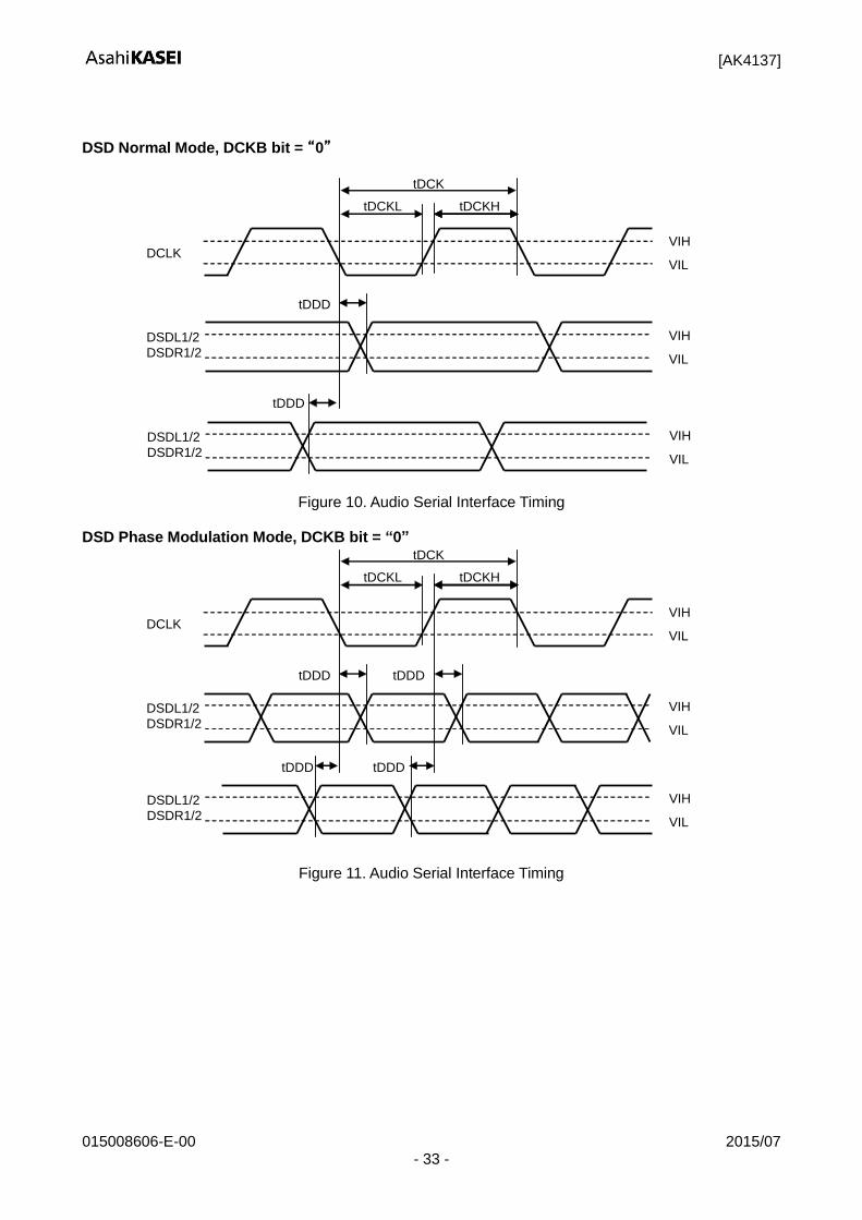
DSD Normal Mode, DCKB bit = “0”
VIH DCLK
VIL
tDDD
VIH DSDL1/2
DSDR1/2 VIL
tDCKH tDCKL
tDCK
tDDD
VIH DSDL1/2
DSDR1/2 VIL
Figure 10. Audio Serial Interface Timing
DSD Phase Modulation Mode, DCKB bit = “0”
VIH DCLK
VIL
tDDD
VIH DSDL1/2
DSDR1/2 VIL
tDCKH tDCKL
tDCK
tDDD
tDDD
VIH DSDL1/2
DSDR1/2 VIL
tDDD
Figure 11. Audio Serial Interface Timing
[AK4137]
015008606-E-00 2015/07 - 34 -
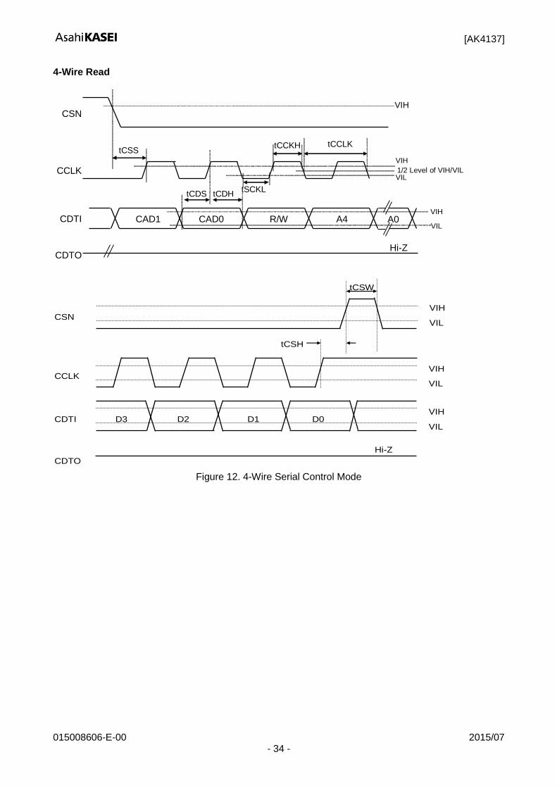
4-Wire Read
tCCKH
CSN
CAD1
VIH
CAD0 R/W A4
tCSS
CCLK
CDTI
tCDS tCDH tSCKL
CDTO
1/2 Level of VIH/VIL
tCCLK
VIH
VIL
A0
Hi-Z
VIH
VIL
tCSW
CSN
CCLK
CDTI D2 D0
tCSH
CDTO
D1 D3
VIH
VIL
VIH
VIL
VIH
VIL
Hi-Z
Figure 12. 4-Wire Serial Control Mode
[AK4137]
015008606-E-00 2015/07 - 35 -
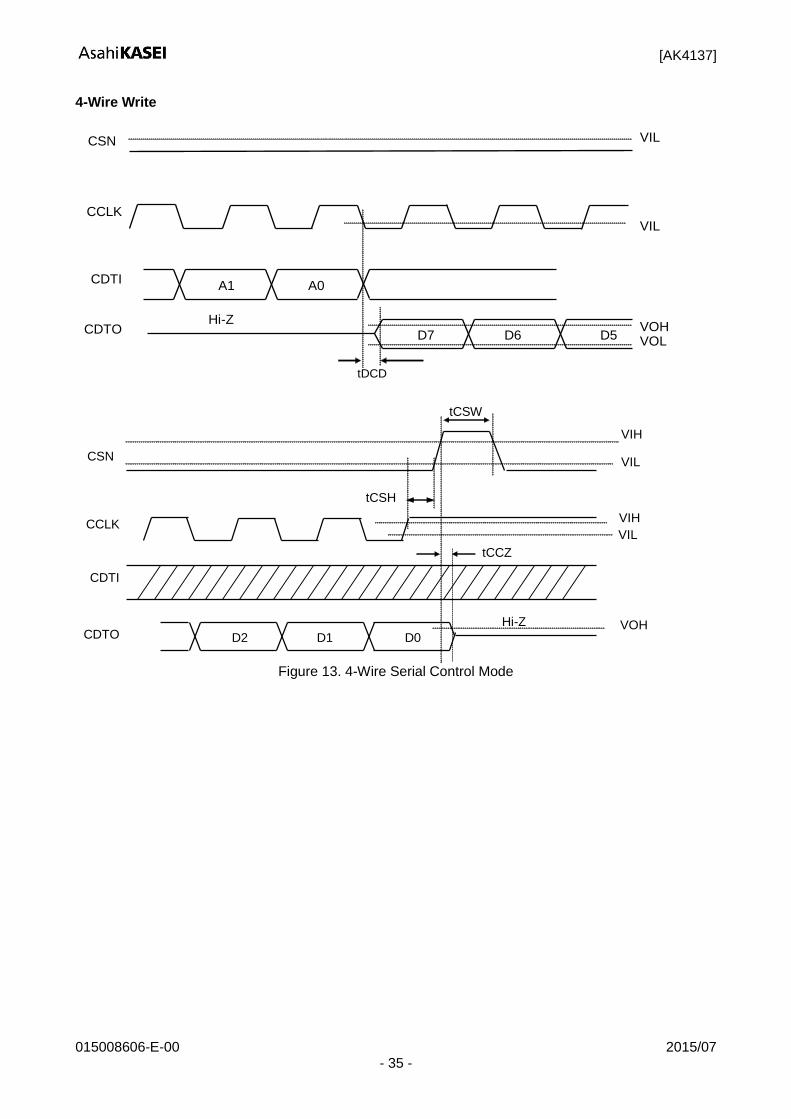
4-Wire Write
CSN
A1 A0
D7 D6
CCLK
CDTI
CDTO D5
tDCD
VIL
VIL
VOH VOL
Hi-Z
CSN VIL
tCSW
CCLK
CDTO D2 D1 D0
CDTI
tCCZ
tCSH
VIH
VIL
VOH
VIH
Hi-Z
Figure 13. 4-Wire Serial Control Mode
[AK4137]
015008606-E-00 2015/07 - 36 -
I2C Bus Control Mode
tHIGH
SCL
SDA
VIH
tLOW tBUF
tHD:STA
tR tF
tHD:DAT tSU:DAT tSU:STA
Stop Start Start Stop
tSU:STO
VIL
VIH
VIL
tSP
Figure 14. I
2C Bus Control Mode
PDN
PDN
DVDD
“L” “H”
VIL
VIH
tAPD2
tPDS
tAPD1
“L” “H”
Figure 15. PDN
[AK4137]
015008606-E-00 2015/07 - 37 -
15. Functional Descriptions
Operation Mode and Setting
Input and Output data format of the AK4137 can be selected by DSDIE bit and DSDOE bit. DOP bit
controls DoP mode and BYPS bit controls bypass mode.
BYPS SRC mode
0
1
SRC
Bypass
Operation mode DOP(*) DSDIE DSDOE INPUT OUTPUT
PCM->PCM 0 0 0 PCM PCM
PCM->DSD 0 0 1 PCM DSD
DSD->PCM 0 1 0 DSD PCM
DSD->DSD 0 1 1 DSD DSD
DoP->PCM 1 0 0 DoP PCM
DoP->DSD 1 0 1 DoP DSD
Not Available 1 1 0 - -
Not Available 1 1 1 - -
(*)This function is not fully DoP Specification compliant and assumes that the DoP signal is input to
the AK4137 with DSD audio data format only. Do not input PCM data when DOP bit = “1”. DoP Marker detection by the AK137 accepts OR results of 0x05, 0xFA and 0xAA resulting in false triggers when PCM data is present.
[AK4137]
015008606-E-00 2015/07 - 38 -
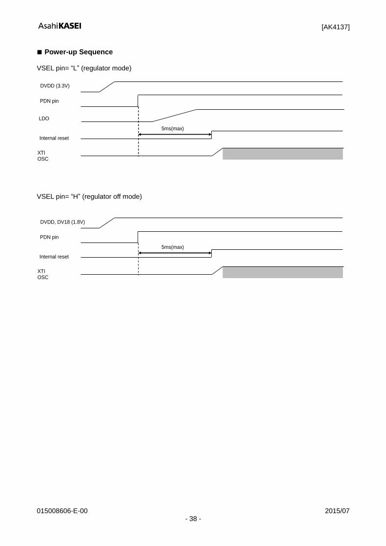
Power-up Sequence
VSEL pin= “L” (regulator mode)
PDN pin
DVDD (3.3V)
LDO
Internal reset
XTI OSC
5ms(max)
VSEL pin= “H” (regulator off mode)
PDN pin
DVDD, DV18 (1.8V)
Internal reset
XTI OSC
5ms(max)
[AK4137]
015008606-E-00 2015/07 - 39 -
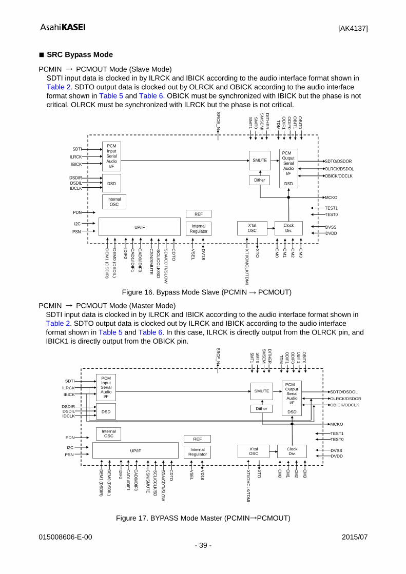
SRC Bypass Mode
PCMIN → PCMOUT Mode (Slave Mode) SDTI input data is clocked in by ILRCK and IBICK according to the audio interface format shown in
Table 2. SDTO output data is clocked out by OLRCK and OBICK according to the audio interface
format shown in Table 5 and Table 6. OBICK must be synchronized with IBICK but the phase is not
critical. OLRCK must be synchronized with ILRCK but the phase is not critical.
PCM Input Serial Audio
I/F
PCM Output Serial Audio
I/F
DSD
OLRCK/DSDOL
OBICK/ODCLK
SDTO/DSDOR
MCKO
DVDD
Internal OSC
DE
M0
(DS
DIL
)
CA
D0
/IDIF
0
SMUTE
X’tal OSC
Clock Div.
UP/IF
Internal
Regulator
REF
DVSS
DE
M1
(DS
DIR
)
CA
D1
/IDIF
1
OD
IF0
OD
IF1
SM
SE
MI
DIT
HE
R
SM
T0
SM
T1
TD
M
SR
CE
_N
TEST1
TEST0
ILRCK
IBICK
SDTI
PDN
PSN
I2C
Dither
IDIF
2
CS
N/S
MU
TE
SC
L/C
CLK
/SD
SD
A/C
DT
I/SL
OW
VS
EL
DV
18
XT
I/OM
CL
K/T
DM
I
XT
O
CM
0
CM
1
CM
2
OB
IT1
OB
IT0
CD
TO
CM
3
DSD DSDIL
IDCLK
DSDIR
Figure 16. Bypass Mode Slave (PCMIN → PCMOUT)
PCMIN → PCMOUT Mode (Master Mode) SDTI input data is clocked in by ILRCK and IBICK according to the audio interface format shown in
Table 2. SDTO output data is clocked out by ILRCK and IBICK according to the audio interface
format shown in Table 5 and Table 6. In this case, ILRCK is directly output from the OLRCK pin, and
IBICK1 is directly output from the OBICK pin.
PCM Input Serial Audio
I/F
PCM Output Serial Audio
I/F
DSD
OLRCK/DSDOR
OBICK/ODCLK
SDTO/DSDOL
MCKO
DVDD
Internal OSC
DE
M0
(DS
DIL
)
CA
D0
/IDIF
0
SMUTE
X’tal OSC
Clock Div.
UP/IF
Internal Regulator
REF
DVSS
DE
M1
(DS
DIR
)
CA
D1
/IDIF
1
OD
IF0
OD
IF1
SM
SE
MI
DIT
HE
R
SM
T0
SM
T1
TD
M
SR
CE
_N
TEST1
TEST0
ILRCK
IBICK
SDTI
PDN
PSN
I2C
Dither
IDIF
2
CS
N/S
MU
TE
SC
L/C
CLK
/SD
SD
A/C
DT
I/SLO
W
VS
EL
VD
18
XT
I/OM
CLK
/TD
MI
XT
O
CM
0
CM
1
CM
2
OB
IT1
OB
IT0
CD
TO
CM
3
DSD DSDIL
IDCLK
DSDIR
Figure 17. BYPASS Mode Master (PCMIN→PCMOUT)
[AK4137]
015008606-E-00 2015/07 - 40 -
DSDIN → DSDOUT Mode (Master Mode)
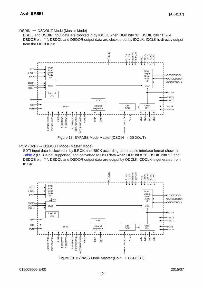
DSDIL and DSDIR input data are clocked in by IDCLK when DOP bit= “0”, DSDIE bit= “1” and DSDOE bit= “1”. DSDOL and DSDOR output data are clocked out by IDCLK. IDCLK is directly output
from the ODCLK pin.
PCM Input Serial Audio
I/F
PCM Output Serial Audio
I/F
DSD
OLRCK/DSDOR
OBICK/ODCLK
SDTO/DSDOL
MCKO
DVDD
Internal OSC
DE
M0
(DS
DIL
)
CA
D0
/IDIF
0
X’tal OSC
Clock Div.
UP/IF
Internal Regulator
REF
DVSS
DE
M1
(DS
DIR
)
CA
D1
/IDIF
1
OD
IF0
OD
IF1
SM
SE
MI
DIT
HE
R
SM
T0
SM
T1
TD
M
SR
CE
_N
TEST1
TEST0
ILRCK
IBICK
SDTI
PDN
PSN
I2C
IDIF
2
CS
N/S
MU
TE
SC
L/C
CLK
/SD
SD
A/C
DT
I/SL
OW
VS
EL
VD
18
XT
I/OM
CL
K/T
DM
I
XT
O
CM
0
CM
1
CM
2
OB
IT1
OB
IT0
CD
TO
CM
3
DSD DSDIL
IDCLK
DSDIR
Figure 18. BYPASS Mode Master (DSDIN → DSDOUT)
PCM (DoP) → DSDOUT Mode (Master Mode)
SDTI input data is clocked in by ILRCK and IBICK according to the audio interface format shown in
Table 2 (LSB is not supported) and converted to DSD data when DOP bit = “1”, DSDIE bit= “0” and
DSDOE bit= “1”. DSDOL and DSDOR output data are output by ODCLK. ODCLK is generated from
IBICK.
PCM Input Serial Audio
I/F
PCM Output Serial Audio
I/F
DSD
OLRCK/DSDOR
OBICK/ODCLK
SDTO/DSDOL
MCKO
DVDD
Internal OSC
DE
M0
(DS
DIL
)
CA
D0
/IDIF
0
X’tal OSC
Clock Div.
UP/IF
Internal Regulator
REF
DVSS
DE
M1
(DS
DIR
)
CA
D1
/IDIF
1
OD
IF0
OD
IF1
SM
SE
MI
DIT
HE
R
SM
T0
SM
T1
TD
M
SR
CE
_N
TEST1
TEST0
ILRCK
IBICK
SDTI
PDN
PSN
I2C
IDIF
2
CS
N/S
MU
TE
SC
L/C
CLK
/SD
SD
A/C
DT
I/SL
OW
VS
EL
VD
18
XT
I/OM
CL
K/T
DM
I
XT
O
CM
0
CM
1
CM
2
OB
IT1
OB
IT0
CD
TO
CM
3
DSD DSDIL
IDCLK
DSDIR
DOP
Figure 19. BYPASS Mode Master (DoP → DSDOUT)
[AK4137]
015008606-E-00 2015/07 - 41 -
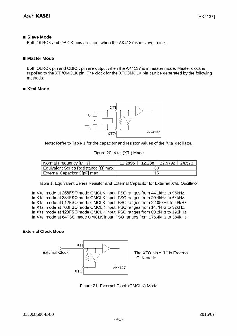
Slave Mode
Both OLRCK and OBICK pins are input when the AK4137 is in slave mode.
Master Mode
Both OLRCK pin and OBICK pin are output when the AK4137 is in master mode. Master clock is supplied to the XTI/OMCLK pin. The clock for the XTI/OMCLK pin can be generated by the following methods.
X’tal Mode
XTI
XTO AK4137
C
C
Note: Refer to Table 1 for the capacitor and resistor values of the X’tal oscillator.
Figure 20. X’tal (XTI) Mode
Normal Frequency [MHz] 11.2896 12.288 22.5792 24.576
Equivalent Series Resistance [Ω] max 60
External Capacitor C[pF] max 15
Table 1. Equivalent Series Resistor and External Capacitor for External X’tal Oscillator
In X’tal mode at 256FSO mode OMCLK input, FSO ranges from 44.1kHz to 96kHz. In X’tal mode at 384FSO mode OMCLK input, FSO ranges from 29.4kHz to 64kHz. In X’tal mode at 512FSO mode OMCLK input, FSO ranges from 22.05kHz to 48kHz. In X’tal mode at 768FSO mode OMCLK input, FSO ranges from 14.7kHz to 32kHz. In X’tal mode at 128FSO mode OMCLK input, FSO ranges from 88.2kHz to 192kHz. In X’tal mode at 64FSO mode OMCLK input, FSO ranges from 176.4kHz to 384kHz.
External Clock Mode
XTI
XTO AK4137
External Clock
Figure 21. External Clock (OMCLK) Mode
The XTO pin = “L” in External CLK mode.
[AK4137]
015008606-E-00 2015/07 - 42 -
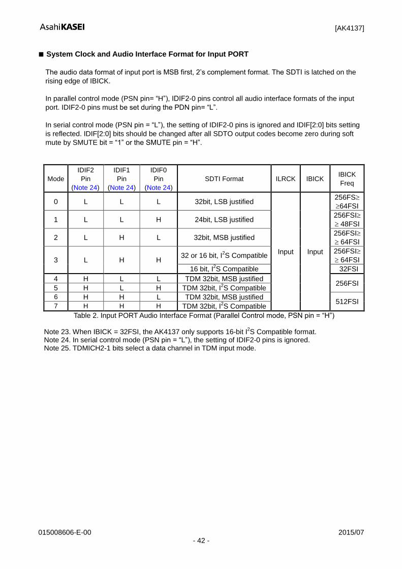
System Clock and Audio Interface Format for Input PORT
The audio data format of input port is MSB first, 2’s complement format. The SDTI is latched on the
rising edge of IBICK.
In parallel control mode (PSN pin= “H”), IDIF2-0 pins control all audio interface formats of the input
port. IDIF2-0 pins must be set during the PDN pin= “L”.
In serial control mode (PSN pin = “L”), the setting of IDIF2-0 pins is ignored and IDIF[2:0] bits setting
is reflected. IDIF[2:0] bits should be changed after all SDTO output codes become zero during soft
mute by SMUTE bit = “1” or the SMUTE pin = “H”.
Mode
IDIF2
Pin
(Note 24)
IDIF1
Pin
(Note 24)
IDIF0
Pin
(Note 24)
SDTI Format ILRCK IBICK IBICK
Freq
0 L L L 32bit, LSB justified
Input Input
256FS
64FSI
1 L L H 24bit, LSB justified 256FSI
48FSI
2 L H L 32bit, MSB justified 256FSI
64FSI
3 L H H 32 or 16 bit, I
2S Compatible
256FSI
64FSI
16 bit, I2S Compatible 32FSI
4 H L L TDM 32bit, MSB justified 256FSI
5 H L H TDM 32bit, I2S Compatible
6 H H L TDM 32bit, MSB justified 512FSI
7 H H H TDM 32bit, I2S Compatible
Table 2. Input PORT Audio Interface Format (Parallel Control mode, PSN pin = “H”) Note 23. When IBICK = 32FSI, the AK4137 only supports 16-bit I
2S Compatible format.
Note 24. In serial control mode (PSN pin = “L”), the setting of IDIF2-0 pins is ignored. Note 25. TDMICH2-1 bits select a data channel in TDM input mode.
[AK4137]
015008606-E-00 2015/07 - 43 -
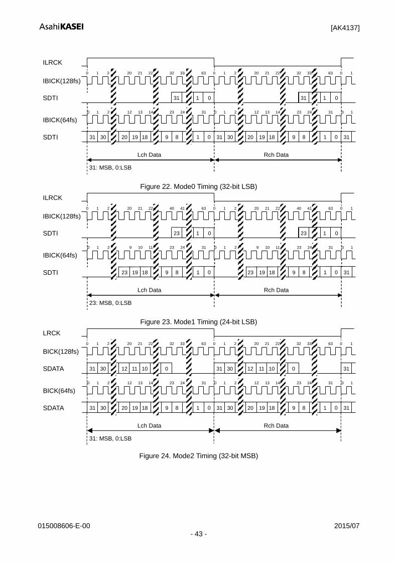
ILRCK
IBICK(128fs)
SDTI
0 1 2 20 21 22 32 33 63 0 1 2 20 21 22 32 33 63 0 1
0 31 1
IBICK(64fs)
SDTI
0 1 2 12 13 14 23 24 31 0 1 2 12 13 14 23 24 31 0
31
1
30 9 31 30 20 19 18 9 31 20 19 18
31: MSB, 0:LSB
8 0 1 8 0 1
Lch Data Rch Data
0 31 1
Figure 22. Mode0 Timing (32-bit LSB)
ILRCK
IBICK(128fs)
SDTI
0 1 2 20 21 22 40 41 63 0 1 2 20 21 22 40
9
41 63 0 1
0 23 1
IBICK(64fs)
SDTI
0 1 2 9 10 11 23 24 31 0 1 2 9 10 11 23 24 31 0 1
9 23 19 18 9 31 23 19 18
23: MSB, 0:LSB
8 0 1 8 0 1
Lch Data Rch Data
0 23 1
Figure 23. Mode1 Timing (24-bit LSB)
LRCK
BICK(128fs)
SDATA
0 1 2 20 21 22 32 33 63 0 1 2 20 21 22 32 33 63 0
31
1
30 0 31 30 12 11 10 0 31 12 11 10
BICK(64fs)
SDATA
0 1 2 12 13 14 23 24 31 0 1 2 12 13 14 23 24 31 0
31
1
30 9 31 30 20 19 18 9 31 20 19 18
31: MSB, 0:LSB
8 0 1 8 0 1
Lch Data Rch Data
Figure 24. Mode2 Timing (32-bit MSB)
[AK4137]
015008606-E-00 2015/07 - 44 -
LRCK
BICK(128fs)
SDATA
0 1 2 20 21 22 33 34 63 0 1 2 20 21 22 33 34 63 0 1
31 0 31 13 12 11 0 13 12 11
BICK(64fs)
SDATA
0 1 2 12 13 14 24 25 31 0 1 2 12 13 14 24 25 31 0
0
1
31 9 0 31 21 20 19 9 0 21 20 19
31: MSB, 0:LSB
8 1 2 8 1 2
Lch Data Rch Data
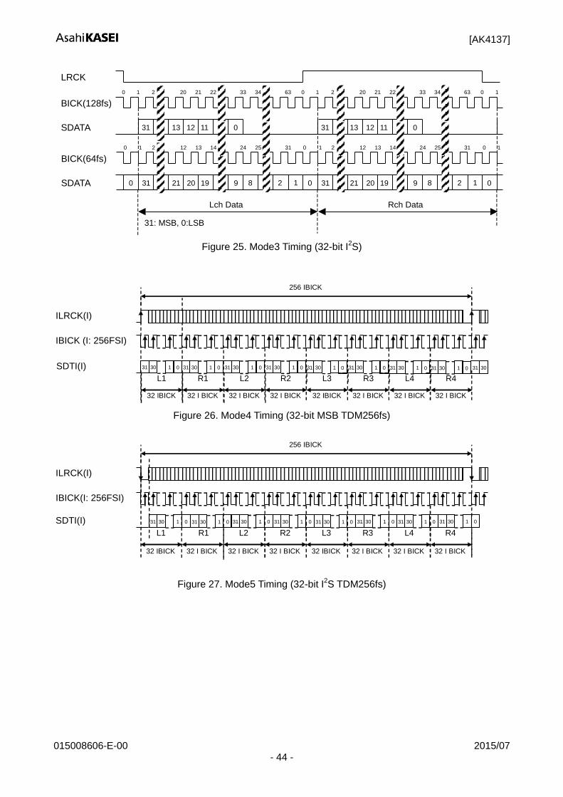
Figure 25. Mode3 Timing (32-bit I
2S)
ILRCK(I)
IBICK (I: 256FSI)
SDTI(I)
L1
32 IBICK
256 IBICK
R1
32 I BICK
L2
32 I BICK
R2
32 I BICK
L3 R3 L4 R4
32 IBICK 32 I BICK 32 I BICK 32 I BICK
31 30 1 0 31 30 1 0 31 30 1 0 31 30 1 0 31 30 1 0 31 30 1 0 31 30 1 0 31 30 1 0 31 30
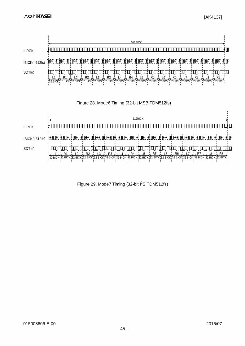
Figure 26. Mode4 Timing (32-bit MSB TDM256fs)
ILRCK(I)
IBICK(I: 256FSI)
SDTI(I)
L1
256 IBICK
R1 L2 R2 L3 R3 L4 R4
32 IBICK 32 I BICK 32 I BICK 32 I BICK 32 IBICK 32 I BICK 32 I BICK 32 I BICK
31 30 1 0 31 30 1 0 31 30 1 0 31 30 1 0 31 30 1 0 31 30 1 0 31 30 1 0 31 30 1 0
Figure 27. Mode5 Timing (32-bit I2S TDM256fs)
[AK4137]
015008606-E-00 2015/07 - 45 -
IBICK(I:512fs)
SDTI(i)
L1 32 BICK
R1 32 BICK
L2 32 BICK
R2 32 BICK
L3 32 BICK
R3 32 BICK
L4 32 BICK
R4 32 BICK 32 BICK 32 BICK 32 BICK 32 BICK 32 BICK 32 BICK
30 31
ILRCK
512BICK
30 1 31 0 30 1 31 0 30 1 31 0 30 1 31 0 30 1 31 0 30 1 31 0 30 1 31 0 30 1 31 0 30 1 31 0 30 1 31 0 30 1 31 0 30 1 31 0 30 1 31 0 30 1 31 0 30 1 31 0 30 1 31 0
32 BICK 32 BICK
L5 R5 L6 R6 L7 R7 L8 R8
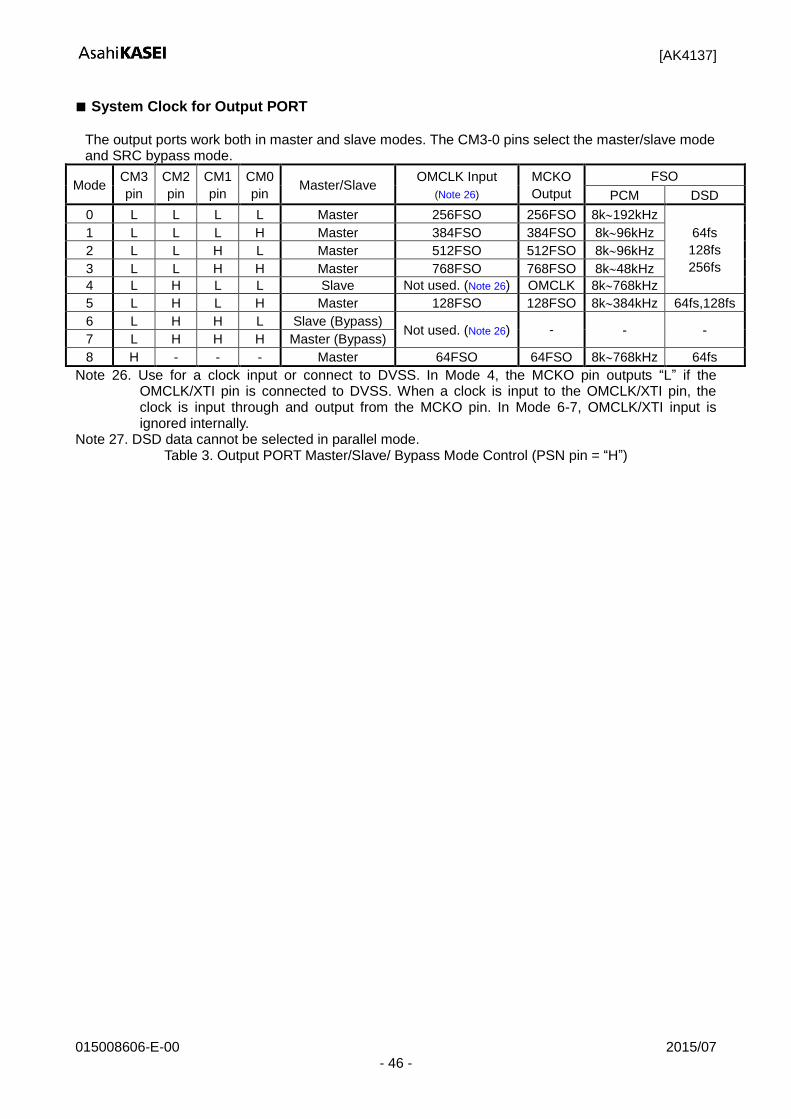
Figure 28. Mode6 Timing (32-bit MSB TDM512fs)
IBICK(I:512fs)
SDTI(i)
L1 32 BICK
R1 32 BICK
L2 32 BICK
R2 32 BICK
L3 32 BICK
R3 32 BICK
L4 32 BICK
R4 32 BICK 32 BICK 32 BICK 32 BICK 32 BICK 32 BICK 32 BICK
30 31
ILRCK
512BICK
30 1 31 0 30 1 31 0 30 1 31 0 30 1 31 0 30 1 31 0 30 1 31 0 30 1 31 0 30 1 31 0 30 1 31 0 30 1 31 0 30 1 31 0 30 1 31 0 30 1 31 0 30 1 31 0 30 1 31 0 30 1 31 0
32 BICK 32 BICK
L5 R5 L6 R6 L7 R7 L8 R8
Figure 29. Mode7 Timing (32-bit I
2S TDM512fs)
[AK4137]
015008606-E-00 2015/07 - 46 -
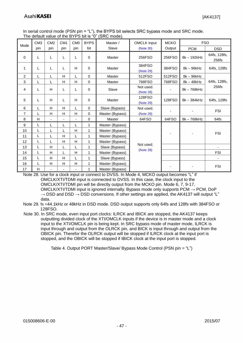
System Clock for Output PORT
The output ports work both in master and slave modes. The CM3-0 pins select the master/slave mode and SRC bypass mode.
Mode CM3
pin
CM2
pin
CM1
pin
CM0
pin Master/Slave
OMCLK Input
(Note 26)
MCKO
Output
FSO
PCM DSD
0 L L L L Master 256FSO 256FSO 8k192kHz
64fs
128fs
256fs
1 L L L H Master 384FSO 384FSO 8k96kHz
2 L L H L Master 512FSO 512FSO 8k96kHz
3 L L H H Master 768FSO 768FSO 8k48kHz
4 L H L L Slave Not used. (Note 26) OMCLK 8k768kHz
5 L H L H Master 128FSO 128FSO 8k384kHz 64fs,128fs
6 L H H L Slave (Bypass) Not used. (Note 26) - - -
7 L H H H Master (Bypass)
8 H - - - Master 64FSO 64FSO 8k768kHz 64fs
Note 26. Use for a clock input or connect to DVSS. In Mode 4, the MCKO pin outputs “L” if the OMCLK/XTI pin is connected to DVSS. When a clock is input to the OMCLK/XTI pin, the clock is input through and output from the MCKO pin. In Mode 6-7, OMCLK/XTI input is ignored internally.
Note 27. DSD data cannot be selected in parallel mode. Table 3. Output PORT Master/Slave/ Bypass Mode Control (PSN pin = “H”)
[AK4137]
015008606-E-00 2015/07 - 47 -
In serial control mode (PSN pin = “L”), the BYPS bit selects SRC bypass mode and SRC mode. The default value of the BYPS bit is “0” (SRC mode).
Mode CM3
pin
CM2
pin
CM1
pin
CM0
pin
BYPS
bit
Master /
Slave
OMCLK Input
(Note 30)
MCKO
Output
FSO
PCM DSD
0 L L L L 0 Master 256FSO 256FSO 8k 192kHz 64fs, 128fs,
256fs
1 L L L H 0 Master 384FSO
(Note 29) 384FSO 8k 96kHz 64fs, 128fs
2 L L H L 0 Master 512FSO 512FSO 8k 96kHz
64fs, 128fs,
256fs
3 L L H H 0 Master 768FSO 768FSO 8k 48kHz
4 L H L L 0 Slave Not used.
(Note 28) - 8k 768kHz
5 L H L H 0 Master 128FSO
(Note 29) 128FSO 8k 384kHz 64fs, 128fs
6 L H H L 0 Slave (Bypass) Not used.
(Note 28) - - FSI
7 L H H H 0 Master (Bypass)
8 H - - - 0 Master 64FSO 64FSO 8k 768kHz 64fs
9 L L L L 1 Master (Bypass)
Not used.
(Note 28)
- - FSI 10 L L L H 1 Master (Bypass)
11 L L H L 1 Master (Bypass)
12 L L H H 1 Master (Bypass)
13 L H L L 1 Slave (Bypass) -
14 L H L H 1 Master (Bypass) FSI
15 L H H L 1 Slave (Bypass) -
16 L H H H 1 Master (Bypass) - - FSI
17 H - - - 1 Master (Bypass)
Note 28. Use for a clock input or connect to DVSS. In Mode 4, MCKO output becomes “L” if OMCLK/XTI/TDMI input is connected to DVSS. In this case, the clock input to the OMCLK/XTI/TDMI pin will be directly output from the MCKO pin. Mode 6, 7, 9-17, OMCLK/XTI/TDMI input is ignored internally. Bypass mode only supports PCM → PCM, DoP → DSD and DSD → DSD conversions. If other settings are applied, the AK4137 will output “L” data.
Note 29. fs =44.1kHz or 48kHz in DSD mode. DSD output supports only 64fs and 128fs with 384FSO or 128FSO.
Note 30. In SRC mode, even input port clocks: ILRCK and IBICK are stopped, the AK4137 keeps outputting divided clock of the XTI/OMCLK inputs if the device is in master mode and a clock input to the XTI/OMCLK pin is being kept. In SRC bypass mode of master mode, ILRCK is input through and output from the OLRCK pin, and BICK is input through and output from the OBICK pin. Therefor the OLRCK output will be stopped if ILRCK clock at the input port is stopped, and the OBICK will be stopped if IBICK clock at the input port is stopped.
Table 4. Output PORT Master/Slave/ Bypass Mode Control (PSN pin = “L”)
[AK4137]
015008606-E-00 2015/07 - 48 -
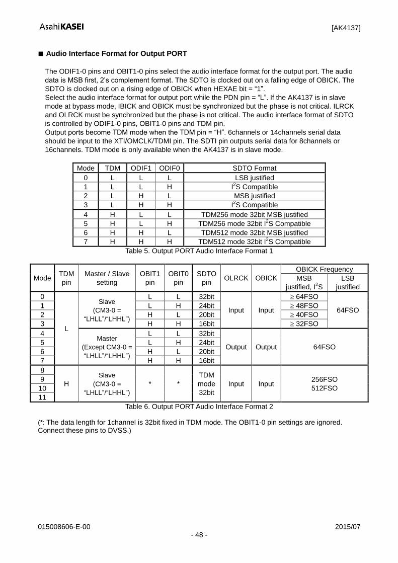
Audio Interface Format for Output PORT
The ODIF1-0 pins and OBIT1-0 pins select the audio interface format for the output port. The audio
data is MSB first, 2’s complement format. The SDTO is clocked out on a falling edge of OBICK. The
SDTO is clocked out on a rising edge of OBICK when HEXAE bit = “1”.
Select the audio interface format for output port while the PDN pin = “L”. If the AK4137 is in slave
mode at bypass mode, IBICK and OBICK must be synchronized but the phase is not critical. ILRCK
and OLRCK must be synchronized but the phase is not critical. The audio interface format of SDTO
is controlled by ODIF1-0 pins, OBIT1-0 pins and TDM pin.
Output ports become TDM mode when the TDM pin = “H”. 6channels or 14channels serial data
should be input to the XTI/OMCLK/TDMI pin. The SDTI pin outputs serial data for 8channels or
16channels. TDM mode is only available when the AK4137 is in slave mode.
Mode TDM ODIF1 ODIF0 SDTO Format
0 L L L LSB justified
1 L L H I2S Compatible
2 L H L MSB justified
3 L H H I2S Compatible
4 H L L TDM256 mode 32bit MSB justified
5 H L H TDM256 mode 32bit I2S Compatible
6 H H L TDM512 mode 32bit MSB justified
7 H H H TDM512 mode 32bit I2S Compatible
Table 5. Output PORT Audio Interface Format 1
Mode TDM
pin
Master / Slave
setting
OBIT1
pin
OBIT0
pin
SDTO
pin OLRCK OBICK
OBICK Frequency
MSB
justified, I2S
LSB
justified
0
L
Slave
(CM3-0 =
“LHLL”/“LHHL”)
L L 32bit
Input Input
64FSO
64FSO 1 L H 24bit 48FSO
2 H L 20bit 40FSO
3 H H 16bit 32FSO
4 Master
(Except CM3-0 =
“LHLL”/“LHHL”)
L L 32bit
Output Output 64FSO 5 L H 24bit
6 H L 20bit
7 H H 16bit
8
H
Slave
(CM3-0 =
“LHLL”/“LHHL”)
* *
TDM
mode
32bit
Input Input 256FSO
512FSO
9
10
11
Table 6. Output PORT Audio Interface Format 2
(*: The data length for 1channel is 32bit fixed in TDM mode. The OBIT1-0 pin settings are ignored. Connect these pins to DVSS.)
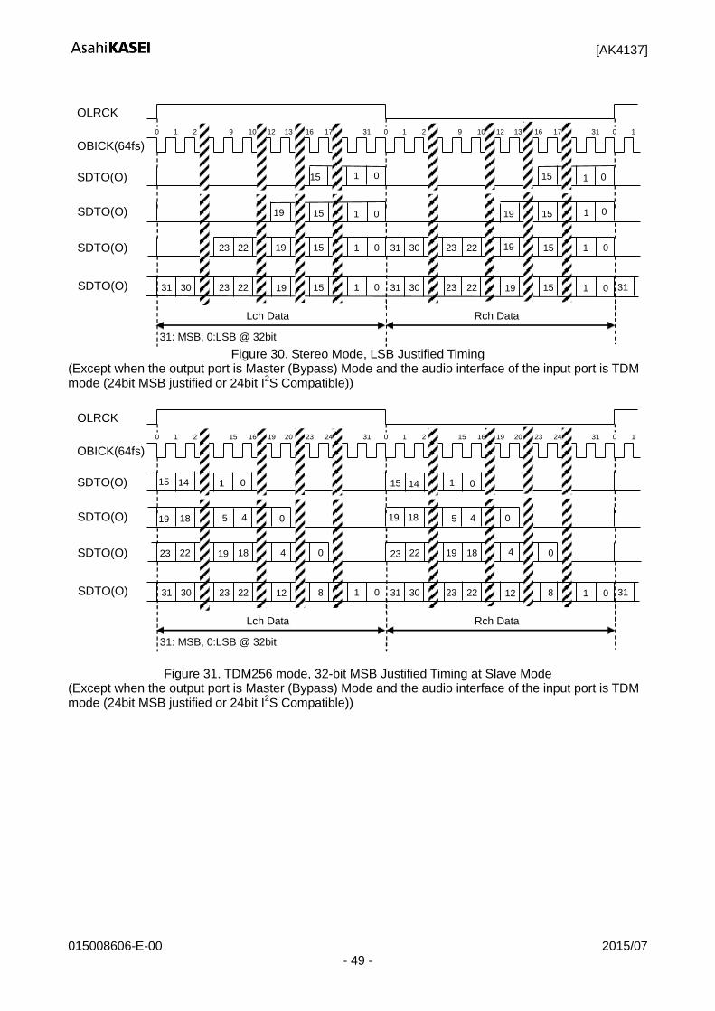
[AK4137]
015008606-E-00 2015/07 - 49 -
OLRCK
OBICK(64fs)
SDTO(O)
0 1 2 9 10 12 16 17 31 0 1 2 9 10 12 16 17 31 0 1
15
SDTO(O) 31 30 23 22
31
23 22 19
31: MSB, 0:LSB @ 32bit
0 1 15 0 1
Lch Data Rch Data
SDTO(O)
SDTO(O) 31 30 23 22 19 0 1
19 15
15
15
0 1
0 1
31 30 23 22 19 15 1 0
19 15 0 1
19
15 0 1
13 13
Figure 30. Stereo Mode, LSB Justified Timing
(Except when the output port is Master (Bypass) Mode and the audio interface of the input port is TDM mode (24bit MSB justified or 24bit I
2S Compatible))
OLRCK
OBICK(64fs)
SDTO(O)
0 1 2 15 16 19 23 24 31 0 1 2 15 16 19 23 24 31 0 1
15
SDTO(O) 23 22 19 18
31
23 18 4
31: MSB, 0:LSB @ 32bit
0
Lch Data Rch Data
SDTO(O)
SDTO(O) 31 30 23 22 12 0 1
19
0
8
0
31 30 23 22 12 8 1 0
19 18 0
4
15 0 1
20 20
22 19
18
14 1
5 4 0
14
5 4
Figure 31. TDM256 mode, 32-bit MSB Justified Timing at Slave Mode (Except when the output port is Master (Bypass) Mode and the audio interface of the input port is TDM mode (24bit MSB justified or 24bit I
2S Compatible))
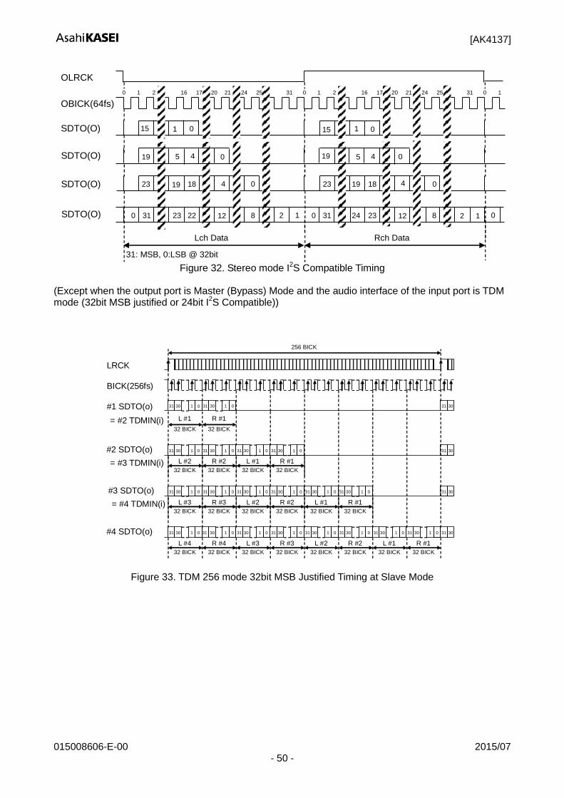
[AK4137]
015008606-E-00 2015/07 - 50 -
OLRCK
OBICK(64fs)
SDTO(O)
0 1 2 16 17 20 24 25 31 0 1 2 16 17 20 24 25 31 0 1
SDTO(O) 23 19 18
0
18 4
31: MSB, 0:LSB @ 32bit
0
Lch Data Rch Data
SDTO(O)
SDTO(O) 0 31 23 22 12 1 2
0
8
0
0 31
31
24 23 12 8 2 1
19 0
4
0 1
21 21
23 19
19
15 1
5 4 0
15
5 4
Figure 32. Stereo mode I
2S Compatible Timing
(Except when the output port is Master (Bypass) Mode and the audio interface of the input port is TDM mode (32bit MSB justified or 24bit I
2S Compatible))
LRCK
BICK(256fs)
#1 SDTO(o) 30 1
L #1
32 BICK
256 BICK
30 1
R #1
32 BICK
31 31
= #2 TDMIN(i)
30 1
L #4
32 BICK
30 1
R #4
32 BICK
30 31 31 31 30 1
L #3
32 BICK
30 1
R #3
32 BICK
31 31 30 1
L #2
32 BICK
30 1
R #2
32 BICK
31 31 30 1
L #1
32 BICK
30 1
R #1
32 BICK
31 31
#2 SDTO(o)
= #3 TDMIN(i)
#3 SDTO(o)
= #4 TDMIN(i)
#4 SDTO(o)
30 1
L #3
32 BICK
30 1
R #3
32 BICK
31 31 30 1
L #2
32 BICK
30 1
R #2
32 BICK
31 31 30 1
L #1
32 BICK
30 1
R #1
32 BICK
31 31 30 31
30 1
L #2
32 BICK
30 1
R #2
32 BICK
31 31 30 1
L #1
32 BICK
30 1
R #1
32 BICK
31 31 30 31
30 31
0
0
0 0 0 0
0 0 0 0 0
0
0 0 0 0 0 0 0 0
Figure 33. TDM 256 mode 32bit MSB Justified Timing at Slave Mode
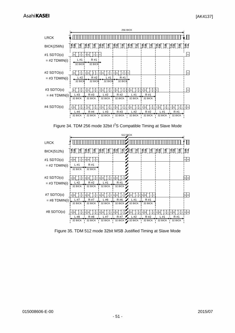
[AK4137]
015008606-E-00 2015/07 - 51 -
LRCK
BICK(256fs)
#1 SDTO(o) 31 2
L #1
32 BICK
256 BICK
31 2
R #1
32 BICK
0 0
= #2 TDMIN(i)
31 2
L #4
32 BICK
31 2
R #4
32 BICK
31 0 0 0 31 2
L #3
32 BICK
31 2
R #3
32 BICK
0 0 31 2
L #2
32 BICK
31 2
R #2
32 BICK
0 0 31 2
L #1
32 BICK
31 2
R #1
32 BICK
0 0
#2 SDTO(o)
= #3 TDMIN(i)
#3 SDTO(o)
= #4 TDMIN(i)
#4 SDTO(o)
31 2
L #3
32 BICK
31 2
R #3
32 BICK
0 0 31 2
L #2
32 BICK
31 2
R #2
32 BICK
0 0 31 2
L #1
32 BICK
31 2
R #1
32 BICK
0 0 31
31 2
L #2
32 BICK
31 2
R #2
32 BICK
0 0 31 2
L #1
32 BICK
31 2
R #1
32 BICK
0 0 31
31
1
1
1 1 1 1
1 1 1 1 1
1
1 1 1 1 1 1 1 1
Figure 34. TDM 256 mode 32bit I2S Compatible Timing at Slave Mode
LRCK
BICK(512fs)
#1 SDTO(o) 30 1
L #1
32 BICK
512 BICK
30 1
R #1
32 BICK
31 31
= #2 TDMIN(i)
30 1
L #8
32 BICK
30 1
R #8
32 BICK
30 31 31 31 30 1
L #7
32 BICK
30 1
R #7
32 BICK
31 31 30 1
L #2
32 BICK
30 1
R #2
32 BICK
31 31 30 1
L #1
32 BICK
30 1
R #1
32 BICK
31 31
#2 SDTO(o)
= #3 TDMIN(i)
#7 SDTO(o)
= #8 TDMIN(i)
#8 SDTO(o)
30 1
L #7
32 BICK
30 1
R #7
32 BICK
31 31 30 1
L #6
32 BICK
30 1
R #6
32 BICK
31 31 30 1
L #1
32 BICK
30 1
R #1
32 BICK
31 31 30 31
30 1
L #2
32 BICK
30 1
R #2
32 BICK
31 31 30 1
L #1
32 BICK
30 1
R #1
32 BICK
31 31 30 31
30 31
0
0
0 0 0 0
0 0 0 0 0
0
0 0 0 0 0 0 0 0
Figure 35. TDM 512 mode 32bit MSB Justified Timing at Slave Mode
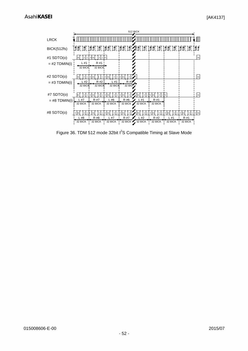
[AK4137]
015008606-E-00 2015/07 - 52 -
LRCK
BICK(512fs)
#1 SDTO(o) 31 2
L #1
32 BICK
512 BICK
31 2
R #1
32 BICK
0 0
= #2 TDMIN(i)
31 2
L #8
32 BICK
31 2
R #8
32 BICK
31 0 0 0 31 2
L #7
32 BICK
31 2
R #7
32 BICK
0 0 31 2
L #2
32 BICK
31 2
R #2
32 BICK
0 0 31 2
L #1
32 BICK
31 2
R #1
32 BICK
0 0
#2 SDTO(o)
= #3 TDMIN(i)
#7 SDTO(o)
= #8 TDMIN(i)
#8 SDTO(o)
31 2
L #7
32 BICK
31 2
R #7
32 BICK
0 0 31 2
L #6
32 BICK
31 2
R #6
32 BICK
0 0 31 2
L #1
32 BICK
31 2
R #1
32 BICK
0 0 31
31 2
L #2
32 BICK
31 2
R #2
32 BICK
0 0 31 2
L #1
32 BICK
31 2
R #1
32 BICK
0 0 31
31
1
1
1 1 1 1
1 1 1 1 1
1
1 1 1 1 1 1 1 1
Figure 36. TDM 512 mode 32bit I2S Compatible Timing at Slave Mode
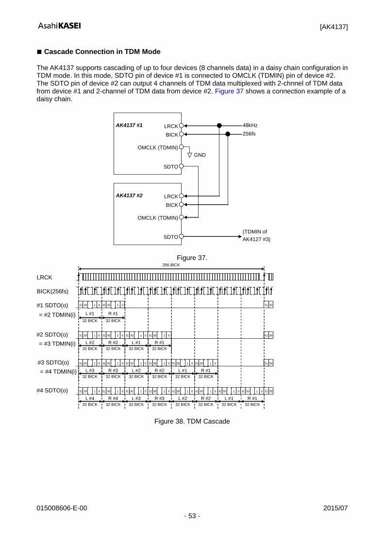
[AK4137]
015008606-E-00 2015/07 - 53 -
Cascade Connection in TDM Mode The AK4137 supports cascading of up to four devices (8 channels data) in a daisy chain configuration in TDM mode. In this mode, SDTO pin of device #1 is connected to OMCLK (TDMIN) pin of device #2. The SDTO pin of device #2 can output 4 channels of TDM data multiplexed with 2-chnnel of TDM data from device #1 and 2-channel of TDM data from device #2. Figure 37 shows a connection example of a daisy chain.
48kHz
256fs
(TDMIN of
AK4127 #3)
LRCK AK4137 #1
BICK
OMCLK (TDMIN)
SDTO
GND
LRCK AK4137 #2
BICK
OMCLK (TDMIN)
SDTO
Figure 37.
LRCK
BICK(256fs)
#1 SDTO(o) 30 1
L #1
32 BICK
256 BICK
30 1
R #1
32 BICK
31 31
= #2 TDMIN(i)
30 1
L #4
32 BICK
30 1
R #4
32 BICK
30 31 31 31 30 1
L #3
32 BICK
30 1
R #3
32 BICK
31 31 30 1
L #2
32 BICK
30 1
R #2
32 BICK
31 31 30 1
L #1
32 BICK
30 1
R #1
32 BICK
31 31
#2 SDTO(o)
= #3 TDMIN(i)
#3 SDTO(o)
= #4 TDMIN(i)
#4 SDTO(o)
30 1
L #3
32 BICK
30 1
R #3
32 BICK
31 31 30 1
L #2
32 BICK
30 1
R #2
32 BICK
31 31 30 1
L #1
32 BICK
30 1
R #1
32 BICK
31 31 30 31
30 1
L #2
32 BICK
30 1
R #2
32 BICK
31 31 30 1
L #1
32 BICK
30 1
R #1
32 BICK
31 31 30 31
30 31
0
0
0 0 0 0
0 0 0 0 0
0
0 0 0 0 0 0 0 0
Figure 38. TDM Cascade
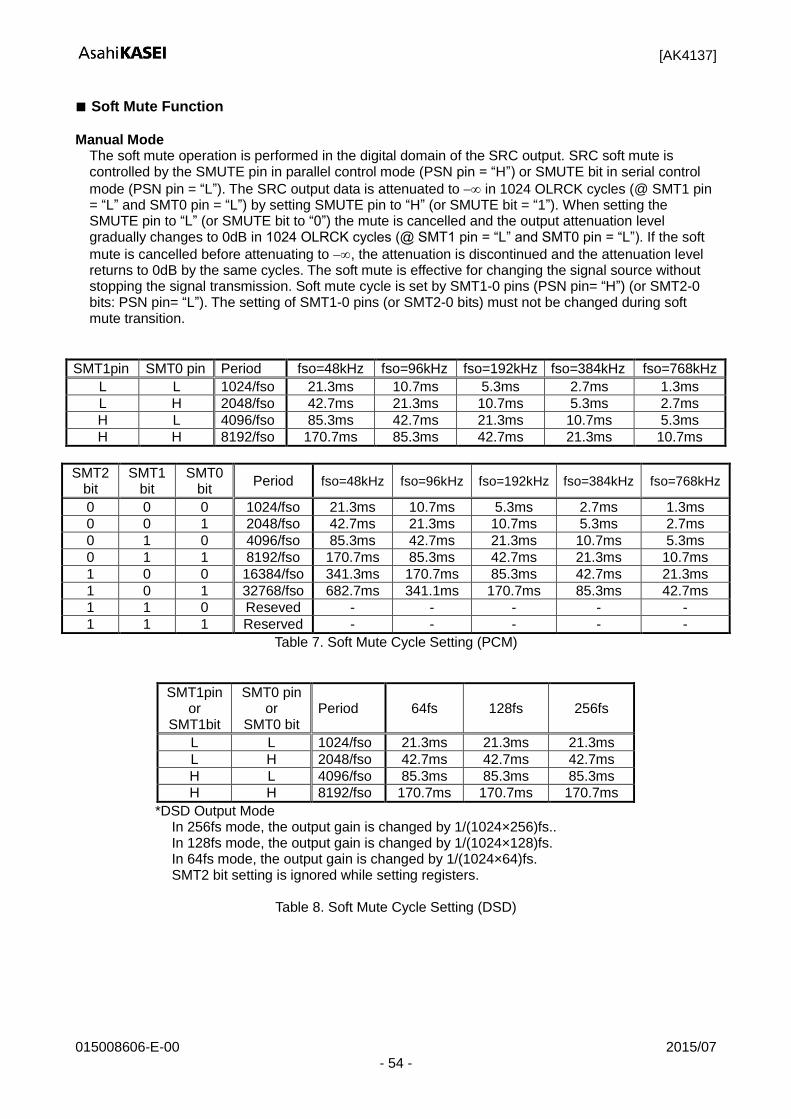
[AK4137]
015008606-E-00 2015/07 - 54 -
Soft Mute Function Manual Mode
The soft mute operation is performed in the digital domain of the SRC output. SRC soft mute is controlled by the SMUTE pin in parallel control mode (PSN pin = “H”) or SMUTE bit in serial control
mode (PSN pin = “L”). The SRC output data is attenuated to in 1024 OLRCK cycles (@ SMT1 pin = “L” and SMT0 pin = “L”) by setting SMUTE pin to “H” (or SMUTE bit = “1”). When setting the SMUTE pin to “L” (or SMUTE bit to “0”) the mute is cancelled and the output attenuation level gradually changes to 0dB in 1024 OLRCK cycles (@ SMT1 pin = “L” and SMT0 pin = “L”). If the soft
mute is cancelled before attenuating to , the attenuation is discontinued and the attenuation level returns to 0dB by the same cycles. The soft mute is effective for changing the signal source without stopping the signal transmission. Soft mute cycle is set by SMT1-0 pins (PSN pin= “H”) (or SMT2-0 bits: PSN pin= “L”). The setting of SMT1-0 pins (or SMT2-0 bits) must not be changed during soft mute transition.
SMT1pin SMT0 pin Period fso=48kHz fso=96kHz fso=192kHz fso=384kHz fso=768kHz
L L 1024/fso 21.3ms 10.7ms 5.3ms 2.7ms 1.3ms
L H 2048/fso 42.7ms 21.3ms 10.7ms 5.3ms 2.7ms
H L 4096/fso 85.3ms 42.7ms 21.3ms 10.7ms 5.3ms
H H 8192/fso 170.7ms 85.3ms 42.7ms 21.3ms 10.7ms
SMT2 bit
SMT1 bit
SMT0 bit
Period fso=48kHz fso=96kHz fso=192kHz fso=384kHz fso=768kHz
0 0 0 1024/fso 21.3ms 10.7ms 5.3ms 2.7ms 1.3ms
0 0 1 2048/fso 42.7ms 21.3ms 10.7ms 5.3ms 2.7ms
0 1 0 4096/fso 85.3ms 42.7ms 21.3ms 10.7ms 5.3ms
0 1 1 8192/fso 170.7ms 85.3ms 42.7ms 21.3ms 10.7ms
1 0 0 16384/fso 341.3ms 170.7ms 85.3ms 42.7ms 21.3ms
1 0 1 32768/fso 682.7ms 341.1ms 170.7ms 85.3ms 42.7ms
1 1 0 Reseved - - - - -
1 1 1 Reserved - - - - -
Table 7. Soft Mute Cycle Setting (PCM)
SMT1pin or
SMT1bit
SMT0 pin or
SMT0 bit Period 64fs 128fs 256fs
L L 1024/fso 21.3ms 21.3ms 21.3ms
L H 2048/fso 42.7ms 42.7ms 42.7ms
H L 4096/fso 85.3ms 85.3ms 85.3ms
H H 8192/fso 170.7ms 170.7ms 170.7ms
*DSD Output Mode In 256fs mode, the output gain is changed by 1/(1024×256)fs.. In 128fs mode, the output gain is changed by 1/(1024×128)fs. In 64fs mode, the output gain is changed by 1/(1024×64)fs. SMT2 bit setting is ignored while setting registers.
Table 8. Soft Mute Cycle Setting (DSD)
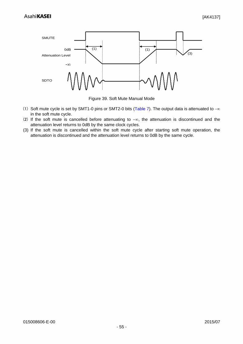
[AK4137]
015008606-E-00 2015/07 - 55 -
SMUTE
Attenuation Level
0dB
-
(1)
(3)
SDTO
(1)
Figure 39. Soft Mute Manual Mode
(1) Soft mute cycle is set by SMT1-0 pins or SMT2-0 bits (Table 7). The output data is attenuated to
in the soft mute cycle. (2) If the soft mute is cancelled before attenuating to , the attenuation is discontinued and the
attenuation level returns to 0dB by the same clock cycles. (3) If the soft mute is cancelled within the soft mute cycle after starting soft mute operation, the
attenuation is discontinued and the attenuation level returns to 0dB by the same cycle.
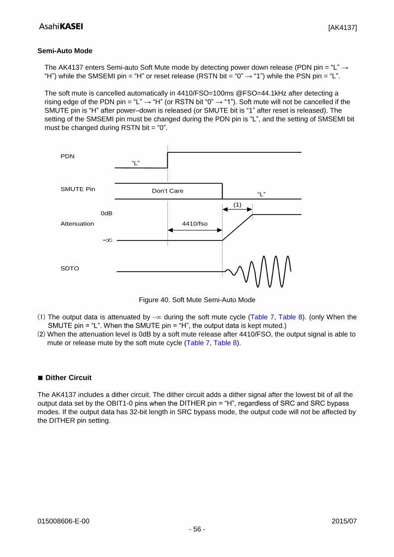
[AK4137]
015008606-E-00 2015/07 - 56 -
Semi-Auto Mode
The AK4137 enters Semi-auto Soft Mute mode by detecting power down release (PDN pin = “L” →
“H”) while the SMSEMI pin = “H” or reset release (RSTN bit = “0” → “1”) while the PSN pin = “L”.
The soft mute is cancelled automatically in 4410/FSO=100ms @FSO=44.1kHz after detecting a
rising edge of the PDN pin = “L” → “H” (or RSTN bit “0” → “1”). Soft mute will not be cancelled if the
SMUTE pin is “H” after power–down is released (or SMUTE bit is “1” after reset is released). The
setting of the SMSEMI pin must be changed during the PDN pin is “L”, and the setting of SMSEMI bit
must be changed during RSTN bit = “0”.
SMUTE Pin
Attenuation
0dB
-
SDTO
4410/fso
(1)
PDN
Don’t Care
“L”
“L”
Figure 40. Soft Mute Semi-Auto Mode
(1) The output data is attenuated by during the soft mute cycle (Table 7, Table 8). (only When the
SMUTE pin = “L”. When the SMUTE pin = “H”, the output data is kept muted.)
(2) When the attenuation level is 0dB by a soft mute release after 4410/FSO, the output signal is able to
mute or release mute by the soft mute cycle (Table 7, Table 8).
Dither Circuit
The AK4137 includes a dither circuit. The dither circuit adds a dither signal after the lowest bit of all the
output data set by the OBIT1-0 pins when the DITHER pin = “H”, regardless of SRC and SRC bypass
modes. If the output data has 32-bit length in SRC bypass mode, the output code will not be affected by
the DITHER pin setting.
[AK4137]
015008606-E-00 2015/07 - 57 -
Digital Filter
The AK4137 has four kinds of digital filters and they are selected by the SD pin (#18) and the SLOW
pin (#17) in parallel control mode (PSN pin = “H”). Different sound qualities on playback can be
selected by these filters. In serial control mode (PSN pin = “L”), the SD pin and the SLOW pin
becomes the SCLK/CCLK pin and the SDA/CDTI pin, respectively and the filter setting by these pins
are ignored.
SD pin SLOW pin Mode
L L Sharp roll-off filter
L H Slow roll-off filter
H L Short delay Sharp roll-off filter
H H Short delay Slow roll-off filter
Table 9. Digital Filter Setting (Parallel Control Mode)
SD bit SLOW bit Mode
0 0 Sharp Roll-off Filter (default)
0 1 Slow Roll-off Filter
1 0 Short delay Sharp Roll-off Filter
1 1 Short delay Slow Roll-off Filter
Table 10. Digital Filter Setting (Serial Control Mode)
De-emphasis Filter
In parallel control mode (PSN pin = “H”), de-emphasis setting of the SRC is controlled by DEM1-0
pins. In serial control mode (PSN pin = “L”), the setting of DEM1-0 pins is ignored.
DEM1pin DEM0 pin Mode
L L 44.1kHz
L H OFF
H L 48kHz
H H 32kHz
Table 11. De-emphasis Filter Setting
Regulator
The AK4137 has an internal regulator which suppresses the voltage to 1.8V from DVDD. The generated 1.8V power is used as power supply for internal circuits only. When an over-current flows into the regulator output, over-current detection circuit will work. When an over-voltage flows into the regulator output, over-voltage detection circuit will work. The regulator block is powered-down and the AK4137 becomes reset state when over-current detection or over-voltage detection is executed. The AK4137 does not return to normal operation without a reset by the PDN pin when these detection circuits are worked. When over-current or over-voltage is detected, the PDN pin should be brought into “L” at once, and set to “H” again to recover normal operation.
The SRCE_N pin indicates the internal status of the device. It outputs “L” in SRC normal operation and outputs “H” when over-current or over-voltage is detected.
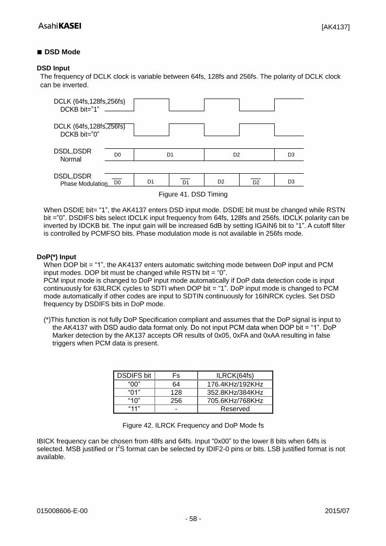
[AK4137]
015008606-E-00 2015/07 - 58 -
DSD Mode DSD Input
The frequency of DCLK clock is variable between 64fs, 128fs and 256fs. The polarity of DCLK clock
can be inverted.
DCLK (64fs,128fs,256fs) DCKB bit=”1”
DCLK (64fs,128fs,256fs) DCKB bit=”0”
DSDL,DSDR Normal
DSDL,DSDR Phase Modulation
D1
D0 D1 D2
D0 D2 D3
D1 D2 D3
Figure 41. DSD Timing
When DSDIE bit= “1”, the AK4137 enters DSD input mode. DSDIE bit must be changed while RSTN bit =”0”. DSDIFS bits select IDCLK input frequency from 64fs, 128fs and 256fs. IDCLK polarity can be inverted by IDCKB bit. The input gain will be increased 6dB by setting IGAIN6 bit to “1”. A cutoff filter is controlled by PCMFSO bits. Phase modulation mode is not available in 256fs mode.
DoP(*) Input
When DOP bit = “1”, the AK4137 enters automatic switching mode between DoP input and PCM input modes. DOP bit must be changed while RSTN bit = “0”. PCM input mode is changed to DoP input mode automatically if DoP data detection code is input continuously for 63ILRCK cycles to SDTI when DOP bit = “1”. DoP input mode is changed to PCM mode automatically if other codes are input to SDTIN continuously for 16INRCK cycles. Set DSD frequency by DSDIFS bits in DoP mode. (*)This function is not fully DoP Specification compliant and assumes that the DoP signal is input to
the AK4137 with DSD audio data format only. Do not input PCM data when DOP bit = “1”. DoP Marker detection by the AK137 accepts OR results of 0x05, 0xFA and 0xAA resulting in false triggers when PCM data is present.
DSDIFS bit Fs ILRCK(64fs)
“00” 64 176.4KHz/192KHz
“01” 128 352.8KHz/384KHz
“10” 256 705.6KHz/768KHz
“11” - Reserved
Figure 42. ILRCK Frequency and DoP Mode fs
IBICK frequency can be chosen from 48fs and 64fs. Input “0x00” to the lower 8 bits when 64fs is selected. MSB justified or I
2S format can be selected by IDIF2-0 pins or bits. LSB justified format is not
available.
[AK4137]
015008606-E-00 2015/07 - 59 -
DSD Output
The AK4137 enters DSD output mode by setting DSDOE bit = “1”. DSDOE bit must be changed while RSTN bit = “0”. 64fs, 128fs and 256fs ODCLK inputs are supported. The output frequency can be chosen by DSDOFS bits. The AK4137 is capable of outputting 64fs, 128fs or 256fs in Master mode. ODCLK polarity can be inverted by ODCKB bit. Input gain can be decreased 6dB by setting ODCKB bit = “1”. The input gain limit is -6dB. The AK4137 cannot output correct data if the input gain exceeds this limit. • Zero Pattern Output If zero input is continued for a certain period, the DSD output is fixed to zero patterns.
ODCLK Frequency Zero Input Period to Zero Patterns
64fs 1023ODCLK
128fs 2047ODCLK
256fs 4095ODCLK
In Zero pattern output, the output is fixed to “1001_0110” in 8ODCLK cycles and it is repeated until zero input is finished. The output returns to normal when zero input is finished. Zero pattern output occurs on Lch and Rch independently. • Input Clip Function Input signal will be clipped internally if a signal that exceeds the limit is input. Clipping process can be set by DSDCLP bits. • Oscillation Detection Function (Error Detection) When an oscillation is detected at the DSD output block, ERRINTL bit becomes “1” for Lch and ERRINTR bit becomes “1” for Rch. The channel that detects an oscillation will become reset state and its output pattern will be fixed to zero. Set RSTN bit to “0” to release Zero pattern fixed output. However, this error detection does not work when a full-scale (0dB) square wave is input. In this case, the output will be -∞ DC (50% duty). (Error detection works if only one code is not matched when the output is clipped.) Oscillation detection function can be ON/OFF by ERRMASK bit (default: ON). Phase modulation mode is not available when ODCLK frequency is 256fs.
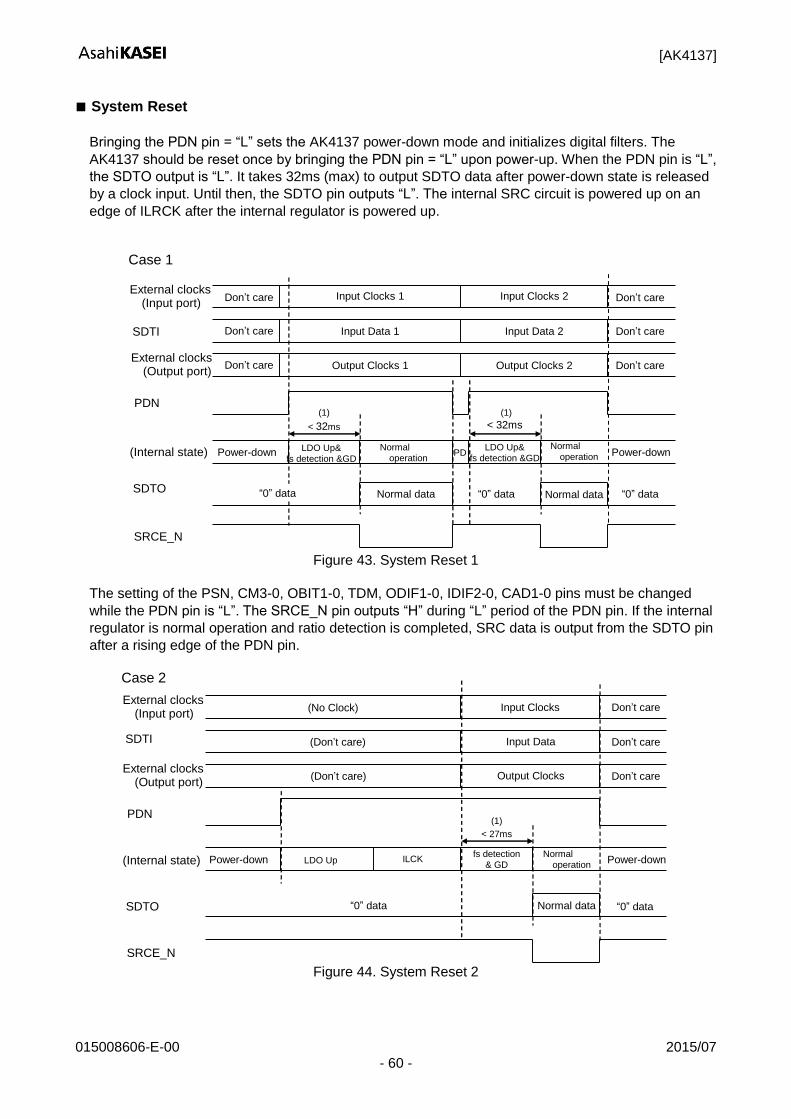
[AK4137]
015008606-E-00 2015/07 - 60 -
System Reset
Bringing the PDN pin = “L” sets the AK4137 power-down mode and initializes digital filters. The
AK4137 should be reset once by bringing the PDN pin = “L” upon power-up. When the PDN pin is “L”,
the SDTO output is “L”. It takes 32ms (max) to output SDTO data after power-down state is released
by a clock input. Until then, the SDTO pin outputs “L”. The internal SRC circuit is powered up on an
edge of ILRCK after the internal regulator is powered up.
Case 1
External clocks (Input port)
SDTI
Don’t care
SDTO
(Internal state) Power-down Normal
operation
< 32ms
Normal data
Input Clocks 1
External clocks (Output port)
Don’t care
Don’t care
PDN
Power-down
Don’t care
Don’t care
Don’t care
“0” data
Normal operation
LDO Up& fs detection &GD
< 32ms
Normal data
PD
Input Data 1
Output Clocks 1
Input Clocks 2
Input Data 2
Output Clocks 2
“0” data “0” data
SRCE_N
(1) (1)
LDO Up& fs detection &GD
Figure 43. System Reset 1
The setting of the PSN, CM3-0, OBIT1-0, TDM, ODIF1-0, IDIF2-0, CAD1-0 pins must be changed
while the PDN pin is “L”. The SRCE_N pin outputs “H” during “L” period of the PDN pin. If the internal
regulator is normal operation and ratio detection is completed, SRC data is output from the SDTO pin
after a rising edge of the PDN pin.
Case 2
External clocks (Input port)
SDTI
SDTO
(Internal state) Power-down Normal
operation
fs detection
& GD
< 27ms
Normal data
(No Clock)
External clocks (Output port)
PDN
Power-down
Don’t care
Don’t care
Don’t care
“0” data
LDO Up
Input Clocks
Input Data
Output Clocks
“0” data
(Don’t care)
(Don’t care)
SRCE_N
(1)
ILCK
Figure 44. System Reset 2
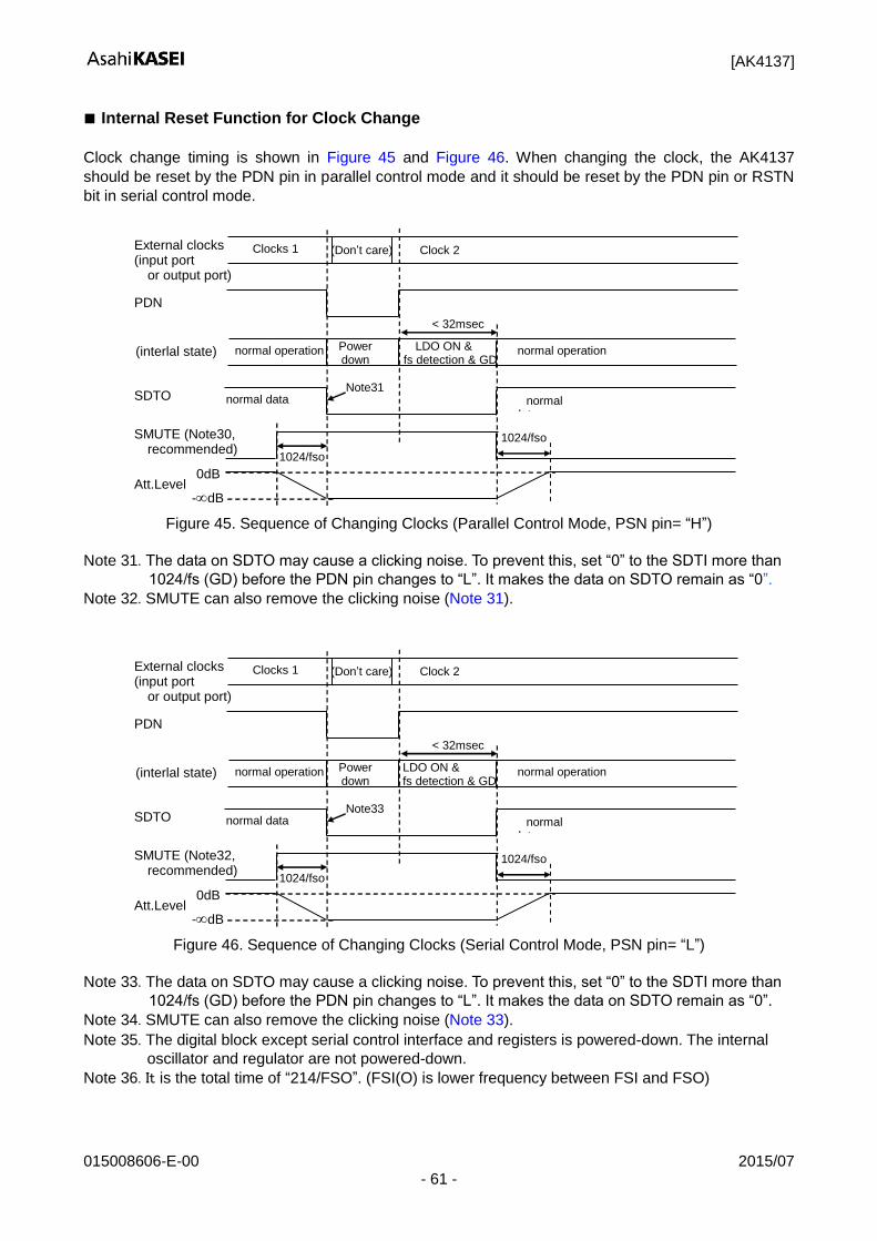
[AK4137]
015008606-E-00 2015/07 - 61 -
Internal Reset Function for Clock Change
Clock change timing is shown in Figure 45 and Figure 46. When changing the clock, the AK4137
should be reset by the PDN pin in parallel control mode and it should be reset by the PDN pin or RSTN
bit in serial control mode.
LDO ON &
fs detection & GD
Power down
External clocks (input port
or output port)
Clocks 1
SDTO
(interlal state) normal operation normal operation
Clock 2 (Don’t care)
< 32msec
SMUTE (Note30, recommended)
1024/fso
Att.Level 0dB
-dB
normal data normal data
1024/fso
PDN
Note31
Figure 45. Sequence of Changing Clocks (Parallel Control Mode, PSN pin= “H”)
Note 31. The data on SDTO may cause a clicking noise. To prevent this, set “0” to the SDTI more than
1024/fs (GD) before the PDN pin changes to “L”. It makes the data on SDTO remain as “0”. Note 32. SMUTE can also remove the clicking noise (Note 31).
LDO ON &
fs detection & GD
Power down
External clocks (input port
or output port)
Clocks 1
SDTO
(interlal state) normal operation normal operation
Clock 2 (Don’t care)
< 32msec
SMUTE (Note32, recommended)
1024/fso
Att.Level 0dB
-dB
normal data normal data
1024/fso
PDN
Note33
Figure 46. Sequence of Changing Clocks (Serial Control Mode, PSN pin= “L”)
Note 33. The data on SDTO may cause a clicking noise. To prevent this, set “0” to the SDTI more than
1024/fs (GD) before the PDN pin changes to “L”. It makes the data on SDTO remain as “0”. Note 34. SMUTE can also remove the clicking noise (Note 33).
Note 35. The digital block except serial control interface and registers is powered-down. The internal
oscillator and regulator are not powered-down. Note 36. It is the total time of “214/FSO”. (FSI(O) is lower frequency between FSI and FSO)
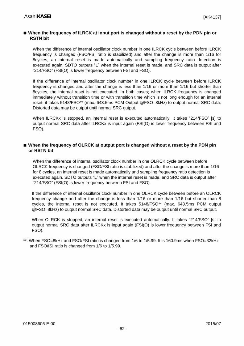
[AK4137]
015008606-E-00 2015/07 - 62 -
When the frequency of ILRCK at input port is changed without a reset by the PDN pin or
RSTN bit
When the difference of internal oscillator clock number in one ILRCK cycle between before ILRCK
frequency is changed (FSO/FSI ratio is stabilized) and after the change is more than 1/16 for
8cycles, an internal reset is made automatically and sampling frequency ratio detection is
executed again. SDTO outputs “L” when the internal reset is made, and SRC data is output after
“214/FSO” (FSI(O) is lower frequency between FSI and FSO).
If the difference of internal oscillator clock number in one ILRCK cycle between before ILRCK
frequency is changed and after the change is less than 1/16 or more than 1/16 but shorter than
8cycles, the internal reset is not executed. In both cases; when ILRCK frequency is changed
immediately without transition time or with transition time which is not long enough for an internal
reset, it takes 5148/FSO** (max. 643.5ms PCM Output @FSO=8kHz) to output normal SRC data.
Distorted data may be output until normal SRC output.
When ILRCKx is stopped, an internal reset is executed automatically. It takes “214/FSO” [s] to
output normal SRC data after ILRCKx is input again (FSI(O) is lower frequency between FSI and
FSO).
When the frequency of OLRCK at output port is changed without a reset by the PDN pin
or RSTN bit
When the difference of internal oscillator clock number in one OLRCK cycle between before
OLRCK frequency is changed (FSO/FSI ratio is stabilized) and after the change is more than 1/16
for 8 cycles, an internal reset is made automatically and sampling frequency ratio detection is
executed again. SDTO outputs “L” when the internal reset is made, and SRC data is output after
“214/FSO” (FSI(O) is lower frequency between FSI and FSO).
If the difference of internal oscillator clock number in one OLRCK cycle between before an OLRCK
frequency change and after the change is less than 1/16 or more than 1/16 but shorter than 8
cycles, the internal reset is not executed. It takes 5148/FSO** (max. 643.5ms PCM output
@FSO=8kHz) to output normal SRC data. Distorted data may be output until normal SRC output.
When OLRCK is stopped, an internal reset is executed automatically. It takes “214/FSO” [s] to
output normal SRC data after ILRCKx is input again (FSI(O) is lower frequency between FSI and
FSO).
**: When FSO=8kHz and FSO/FSI ratio is changed from 1/6 to 1/5.99. It is 160.9ms when FSO=32kHz
and FSO/fSI ratio is changed from 1/6 to 1/5.99.
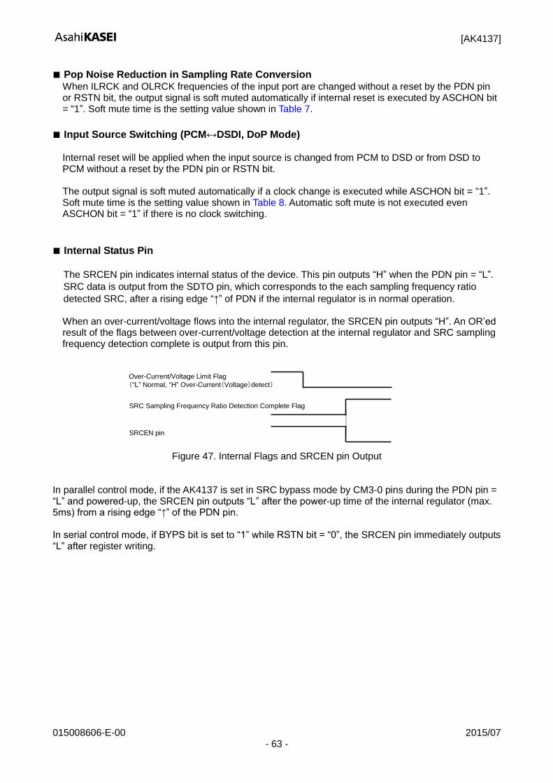
[AK4137]
015008606-E-00 2015/07 - 63 -
Over-Current/Voltage Limit Flag
(“L” Normal, “H” Over-Current(Voltage)detect)
SRC Sampling Frequency Ratio Detection Complete Flag
SRCEN pin
Pop Noise Reduction in Sampling Rate Conversion When ILRCK and OLRCK frequencies of the input port are changed without a reset by the PDN pin or RSTN bit, the output signal is soft muted automatically if internal reset is executed by ASCHON bit = “1”. Soft mute time is the setting value shown in Table 7.
Input Source Switching (PCM↔DSDI, DoP Mode)
Internal reset will be applied when the input source is changed from PCM to DSD or from DSD to PCM without a reset by the PDN pin or RSTN bit. The output signal is soft muted automatically if a clock change is executed while ASCHON bit = “1”. Soft mute time is the setting value shown in Table 8. Automatic soft mute is not executed even ASCHON bit = “1” if there is no clock switching.
Internal Status Pin
The SRCEN pin indicates internal status of the device. This pin outputs “H” when the PDN pin = “L”.
SRC data is output from the SDTO pin, which corresponds to the each sampling frequency ratio
detected SRC, after a rising edge “↑” of PDN if the internal regulator is in normal operation. When an over-current/voltage flows into the internal regulator, the SRCEN pin outputs “H”. An OR’ed result of the flags between over-current/voltage detection at the internal regulator and SRC sampling frequency detection complete is output from this pin.
Figure 47. Internal Flags and SRCEN pin Output In parallel control mode, if the AK4137 is set in SRC bypass mode by CM3-0 pins during the PDN pin = “L” and powered-up, the SRCEN pin outputs “L” after the power-up time of the internal regulator (max. 5ms) from a rising edge “↑” of the PDN pin. In serial control mode, if BYPS bit is set to “1” while RSTN bit = “0”, the SRCEN pin immediately outputs “L” after register writing.
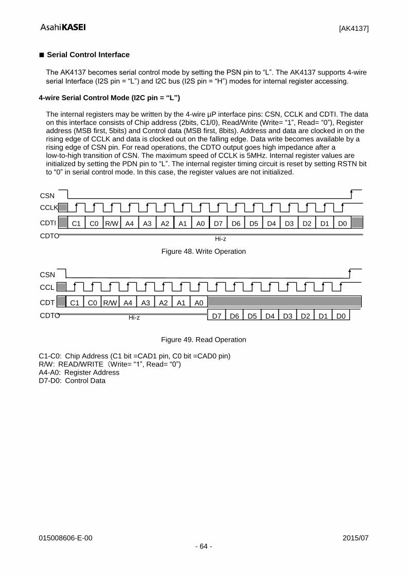
[AK4137]
015008606-E-00 2015/07 - 64 -
Serial Control Interface
The AK4137 becomes serial control mode by setting the PSN pin to “L”. The AK4137 supports 4-wire
serial Interface (I2S pin = “L”) and I2C bus (I2S pin = “H”) modes for internal register accessing. 4-wire Serial Control Mode (I2C pin = “L”)
The internal registers may be written by the 4-wire µP interface pins: CSN, CCLK and CDTI. The data on this interface consists of Chip address (2bits, C1/0), Read/Write (Write= “1”, Read= “0”), Register address (MSB first, 5bits) and Control data (MSB first, 8bits). Address and data are clocked in on the rising edge of CCLK and data is clocked out on the falling edge. Data write becomes available by a rising edge of CSN pin. For read operations, the CDTO output goes high impedance after a lowtohigh transition of CSN. The maximum speed of CCLK is 5MHz. Internal register values are initialized by setting the PDN pin to “L”. The internal register timing circuit is reset by setting RSTN bit to “0” in serial control mode. In this case, the register values are not initialized.
Figure 48. Write Operation
Figure 49. Read Operation
C1-C0: Chip Address (C1 bit =CAD1 pin, C0 bit =CAD0 pin) R/W: READ/WRITE (Write= “1”, Read= “0”) A4-A0: Register Address D7-D0: Control Data
C1
C0 R/W A4 A3 A2 A1 A0 D7 D6 D5 D4 D3 D2 D1 D0
CSN
CCLK
CDTI
CDTO Hi-z
C1 C0 R/W A4 A3 A2 A1 A0
D7 D6 D5 D4 D3 D2 D1 D0
CSN
CCL
K CDT
I CDTO Hi-z
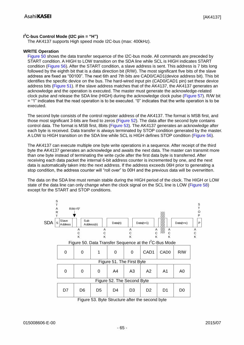
[AK4137]
015008606-E-00 2015/07 - 65 -
I2C-bus Control Mode (I2C pin = “H”) The AK4137 supports High speed mode I2C-bus (max: 400kHz).
WRITE Operation
Figure 50 shows the data transfer sequence of the I2C-bus mode. All commands are preceded by START condition. A HIGH to LOW transition on the SDA line while SCL is HIGH indicates START condition (Figure 56). After the START condition, a slave address is sent. This address is 7 bits long followed by the eighth bit that is a data direction bit (R/W). The most significant five bits of the slave address are fixed as “00100”. The next 6th and 7th bits are CAD0/CAD1(device address bit). This bit identifies the specific device on the bus. The hard-wired input pin (CAD0/CAD1 pin) set these device address bits (Figure 51). If the slave address matches that of the AK4137, the AK4137 generates an acknowledge and the operation is executed. The master must generate the acknowledge-related clock pulse and release the SDA line (HIGH) during the acknowledge clock pulse (Figure 57). R/W bit = “1” indicates that the read operation is to be executed. “0” indicates that the write operation is to be executed. The second byte consists of the control register address of the AK4137. The format is MSB first, and those most significant 3-bits are fixed to zeros (Figure 52). The data after the second byte contains control data. The format is MSB first, 8bits (Figure 53). The AK4137 generates an acknowledge after each byte is received. Data transfer is always terminated by STOP condition generated by the master. A LOW to HIGH transition on the SDA line while SCL is HIGH defines STOP condition (Figure 56).
The AK4137 can execute multiple one byte write operations in a sequence. After receipt of the third byte the AK4137 generates an acknowledge and awaits the next data. The master can transmit more than one byte instead of terminating the write cycle after the first data byte is transferred. After receiving each data packet the internal 6-bit address counter is incremented by one, and the next data is automatically taken into the next address. If the address exceeds 06H prior to generating a stop condition, the address counter will “roll over” to 00H and the previous data will be overwritten. The data on the SDA line must remain stable during the HIGH period of the clock. The HIGH or LOW state of the data line can only change when the clock signal on the SCL line is LOW (Figure 58) except for the START and STOP conditions.
SDASlave
AddressS
S
T
A
R
T
R/W="0"
A
C
K
Sub
Address(n)
A
C
K
Data(n)
A
C
K
Data(n+1)
A
C
K
A
C
K
Data(n+x)
A
C
K
P
S
T
O
P
Figure 50. Data Transfer Sequence at the I
2C-Bus Mode
0 0 1 0 0 CAD1 CAD0 R/W
Figure 51. The First Byte
0 0 0 A4 A3 A2 A1 A0
Figure 52. The Second Byte
D7 D6 D5 D4 D3 D2 D1 D0
Figure 53. Byte Structure after the second byte
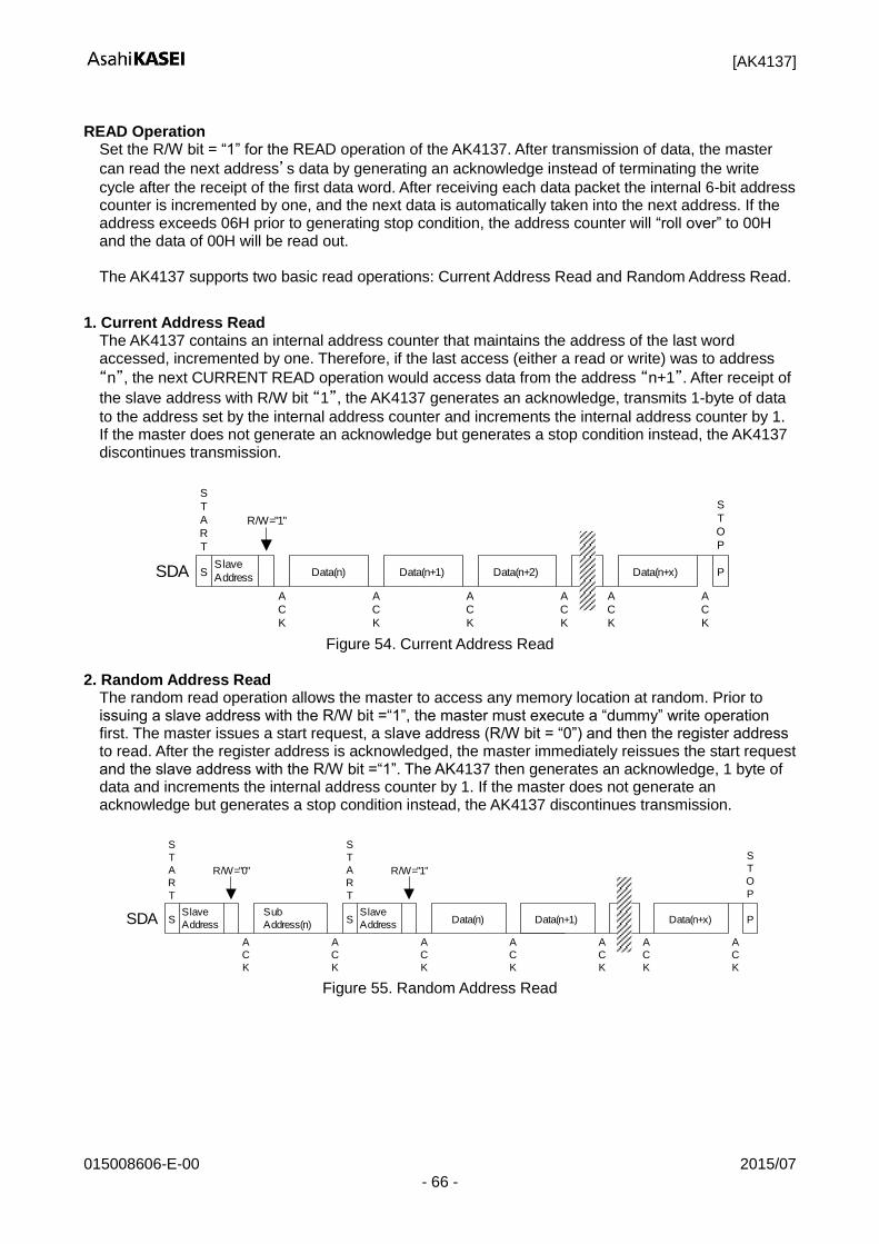
[AK4137]
015008606-E-00 2015/07 - 66 -
READ Operation
Set the R/W bit = “1” for the READ operation of the AK4137. After transmission of data, the master
can read the next address’s data by generating an acknowledge instead of terminating the write
cycle after the receipt of the first data word. After receiving each data packet the internal 6-bit address counter is incremented by one, and the next data is automatically taken into the next address. If the address exceeds 06H prior to generating stop condition, the address counter will “roll over” to 00H and the data of 00H will be read out. The AK4137 supports two basic read operations: Current Address Read and Random Address Read.
1. Current Address Read
The AK4137 contains an internal address counter that maintains the address of the last word accessed, incremented by one. Therefore, if the last access (either a read or write) was to address
“n”, the next CURRENT READ operation would access data from the address “n+1”. After receipt of
the slave address with R/W bit “1”, the AK4137 generates an acknowledge, transmits 1-byte of data
to the address set by the internal address counter and increments the internal address counter by 1. If the master does not generate an acknowledge but generates a stop condition instead, the AK4137 discontinues transmission.
SDASlave
AddressS
S
T
A
R
T
R/W="1"
A
C
K
A
C
K
Data(n+1)
A
C
K
Data(n+2)
A
C
K
A
C
K
Data(n+x)
A
C
K
P
S
T
O
P
Data(n)
Figure 54. Current Address Read
2. Random Address Read
The random read operation allows the master to access any memory location at random. Prior to issuing a slave address with the R/W bit =“1”, the master must execute a “dummy” write operation first. The master issues a start request, a slave address (R/W bit = “0”) and then the register address to read. After the register address is acknowledged, the master immediately reissues the start request and the slave address with the R/W bit =“1”. The AK4137 then generates an acknowledge, 1 byte of data and increments the internal address counter by 1. If the master does not generate an acknowledge but generates a stop condition instead, the AK4137 discontinues transmission.
SDASlave
AddressS
S
T
A
R
T
R/W="0"
A
C
K
A
C
K
A
C
K
Data(n)
A
C
K
Data(n+x)
A
C
K
P
S
T
O
P
Sub
Address(n)S
Slave
Address
R/W="1"
S
T
A
R
T
Data(n+1)
A
C
K
A
C
K
Figure 55. Random Address Read
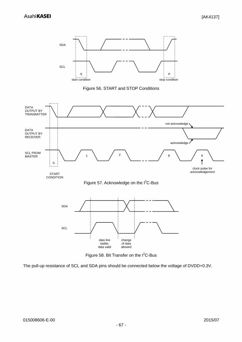
[AK4137]
015008606-E-00 2015/07 - 67 -
SCL
SDA
stop conditionstart condition
S P
Figure 56. START and STOP Conditions
SCL FROMMASTER
acknowledge
DATAOUTPUT BYTRANSMITTER
DATAOUTPUT BYRECEIVER
1 98
STARTCONDITION
not acknowledge
clock pulse foracknowledgement
S
2
Figure 57. Acknowledge on the I
2C-Bus
SCL
SDA
data linestable;
data valid
changeof dataallowed
Figure 58. Bit Transfer on the I
2C-Bus
The pull-up resistance of SCL and SDA pins should be connected below the voltage of DVDD+0.3V.
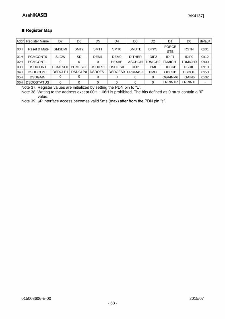
[AK4137]
015008606-E-00 2015/07 - 68 -
Register Map
Addr Register Name D7 D6 D5 D4 D3 D2 D1 D0 default
00H Reset & Mute SMSEMI SMT2 SMT1 SMT0 SMUTE BYPS FORCE
STB RSTN 0x01
01H PCMCONT0 SLOW SD DEM1 DEM0 DITHER IDIF2 IDIF1 IDIF0 0x12
02H PCMCONT1 0 0 0 HEXAE ASCHON TDMICH2 TDMICH1 TDMICH0 0x00
03H DSDICONT PCMFSO1 PCMFSO0 DSDIFS1 DSDIFS0 DOP PMI IDCKB DSDIE 0x10
04H DSDOCONT DSDCLP1 DSDCLP0 DSDOFS1 DSDOFS0 ERRMASK PMO ODCKB DSDOE 0x50
05H DSDGAIN 0 0 0 0 0 0 OGAINM6 IGAIN6 0x02
06H DSDOSTATUS 0 0 0 0 0 0 ERRINTR ERRINTL -
Note 37. Register values are initialized by setting the PDN pin to “L”. Note 38. Writing to the address except 00H ~ 06H is prohibited. The bits defined as 0 must contain a “0”
value. Note 39. µP interface access becomes valid 5ms (max) after from the PDN pin “↑”.
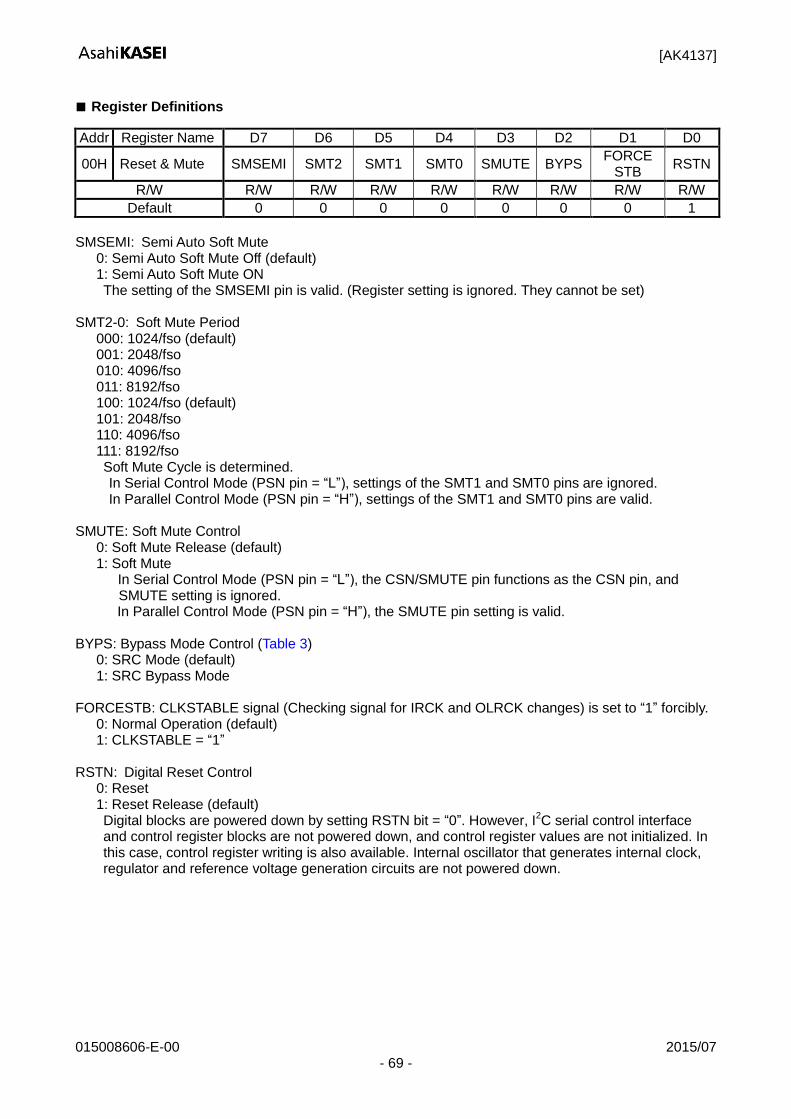
[AK4137]
015008606-E-00 2015/07 - 69 -
Register Definitions
Addr Register Name D7 D6 D5 D4 D3 D2 D1 D0
00H Reset & Mute SMSEMI SMT2 SMT1 SMT0 SMUTE BYPS FORCE
STB RSTN
R/W R/W R/W R/W R/W R/W R/W R/W R/W
Default 0 0 0 0 0 0 0 1
SMSEMI: Semi Auto Soft Mute
0: Semi Auto Soft Mute Off (default) 1: Semi Auto Soft Mute ON The setting of the SMSEMI pin is valid. (Register setting is ignored. They cannot be set)
SMT2-0: Soft Mute Period
000: 1024/fso (default) 001: 2048/fso 010: 4096/fso 011: 8192/fso 100: 1024/fso (default) 101: 2048/fso 110: 4096/fso 111: 8192/fso Soft Mute Cycle is determined. In Serial Control Mode (PSN pin = “L”), settings of the SMT1 and SMT0 pins are ignored. In Parallel Control Mode (PSN pin = “H”), settings of the SMT1 and SMT0 pins are valid.
SMUTE: Soft Mute Control
0: Soft Mute Release (default) 1: Soft Mute
In Serial Control Mode (PSN pin = “L”), the CSN/SMUTE pin functions as the CSN pin, and SMUTE setting is ignored. In Parallel Control Mode (PSN pin = “H”), the SMUTE pin setting is valid.
BYPS: Bypass Mode Control (Table 3)
0: SRC Mode (default) 1: SRC Bypass Mode
FORCESTB: CLKSTABLE signal (Checking signal for IRCK and OLRCK changes) is set to “1” forcibly.
0: Normal Operation (default) 1: CLKSTABLE = “1”
RSTN: Digital Reset Control
0: Reset 1: Reset Release (default) Digital blocks are powered down by setting RSTN bit = “0”. However, I
2C serial control interface
and control register blocks are not powered down, and control register values are not initialized. In this case, control register writing is also available. Internal oscillator that generates internal clock, regulator and reference voltage generation circuits are not powered down.
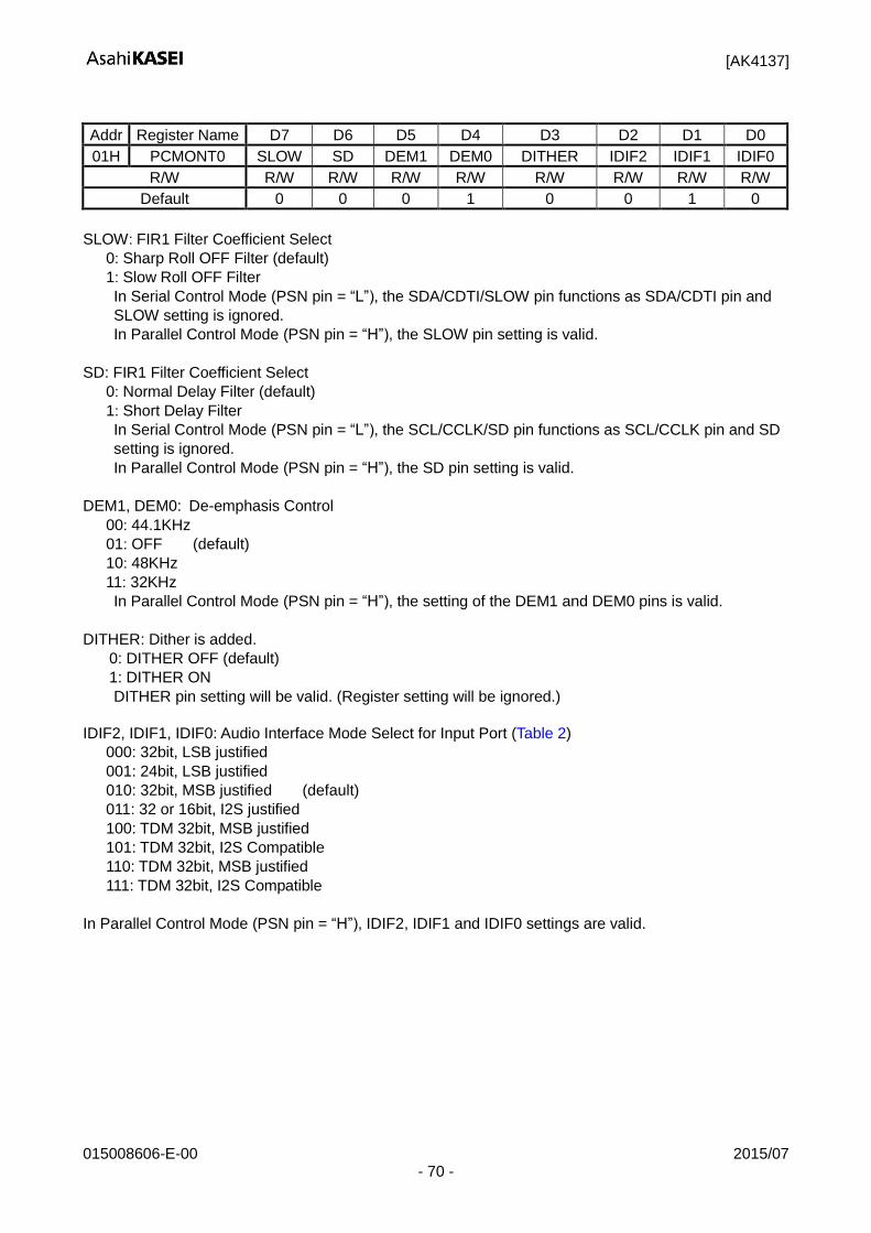
[AK4137]
015008606-E-00 2015/07 - 70 -
Addr Register Name D7 D6 D5 D4 D3 D2 D1 D0
01H PCMONT0 SLOW SD DEM1 DEM0 DITHER IDIF2 IDIF1 IDIF0
R/W R/W R/W R/W R/W R/W R/W R/W R/W
Default 0 0 0 1 0 0 1 0
SLOW: FIR1 Filter Coefficient Select
0: Sharp Roll OFF Filter (default)
1: Slow Roll OFF Filter
In Serial Control Mode (PSN pin = “L”), the SDA/CDTI/SLOW pin functions as SDA/CDTI pin and
SLOW setting is ignored.
In Parallel Control Mode (PSN pin = “H”), the SLOW pin setting is valid.
SD: FIR1 Filter Coefficient Select
0: Normal Delay Filter (default)
1: Short Delay Filter
In Serial Control Mode (PSN pin = “L”), the SCL/CCLK/SD pin functions as SCL/CCLK pin and SD
setting is ignored.
In Parallel Control Mode (PSN pin = “H”), the SD pin setting is valid.
DEM1, DEM0: De-emphasis Control
00: 44.1KHz
01: OFF (default)
10: 48KHz
11: 32KHz
In Parallel Control Mode (PSN pin = “H”), the setting of the DEM1 and DEM0 pins is valid.
DITHER: Dither is added.
0: DITHER OFF (default)
1: DITHER ON
DITHER pin setting will be valid. (Register setting will be ignored.)
IDIF2, IDIF1, IDIF0: Audio Interface Mode Select for Input Port (Table 2)
000: 32bit, LSB justified
001: 24bit, LSB justified
010: 32bit, MSB justified (default)
011: 32 or 16bit, I2S justified
100: TDM 32bit, MSB justified
101: TDM 32bit, I2S Compatible
110: TDM 32bit, MSB justified
111: TDM 32bit, I2S Compatible
In Parallel Control Mode (PSN pin = “H”), IDIF2, IDIF1 and IDIF0 settings are valid.
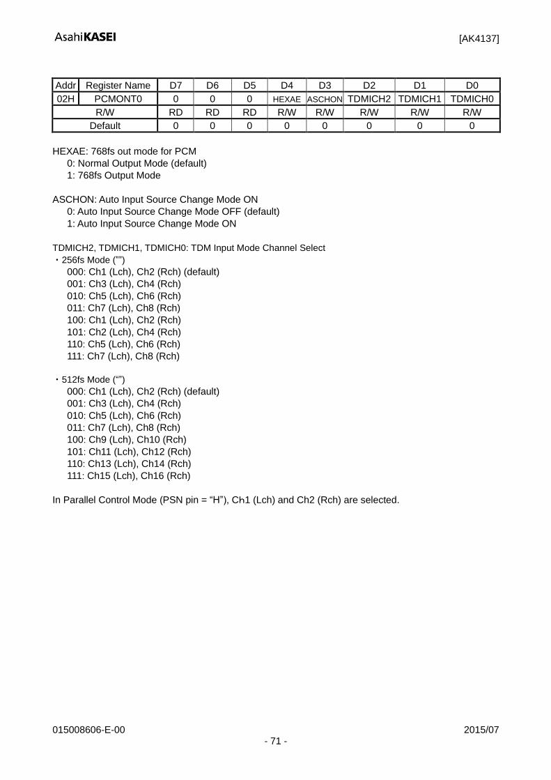
[AK4137]
015008606-E-00 2015/07 - 71 -
Addr Register Name D7 D6 D5 D4 D3 D2 D1 D0
02H PCMONT0 0 0 0 HEXAE ASCHON TDMICH2 TDMICH1 TDMICH0
R/W RD RD RD R/W R/W R/W R/W R/W
Default 0 0 0 0 0 0 0 0
HEXAE: 768fs out mode for PCM
0: Normal Output Mode (default)
1: 768fs Output Mode
ASCHON: Auto Input Source Change Mode ON
0: Auto Input Source Change Mode OFF (default)
1: Auto Input Source Change Mode ON
TDMICH2, TDMICH1, TDMICH0: TDM Input Mode Channel Select
・256fs Mode (””)
000: Ch1 (Lch), Ch2 (Rch) (default)
001: Ch3 (Lch), Ch4 (Rch)
010: Ch5 (Lch), Ch6 (Rch)
011: Ch7 (Lch), Ch8 (Rch)
100: Ch1 (Lch), Ch2 (Rch)
101: Ch2 (Lch), Ch4 (Rch)
110: Ch5 (Lch), Ch6 (Rch)
111: Ch7 (Lch), Ch8 (Rch)
・512fs Mode (“”)
000: Ch1 (Lch), Ch2 (Rch) (default)
001: Ch3 (Lch), Ch4 (Rch)
010: Ch5 (Lch), Ch6 (Rch)
011: Ch7 (Lch), Ch8 (Rch)
100: Ch9 (Lch), Ch10 (Rch)
101: Ch11 (Lch), Ch12 (Rch)
110: Ch13 (Lch), Ch14 (Rch)
111: Ch15 (Lch), Ch16 (Rch)
In Parallel Control Mode (PSN pin = “H”), Ch1 (Lch) and Ch2 (Rch) are selected.
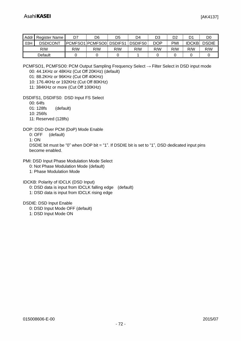
[AK4137]
015008606-E-00 2015/07 - 72 -
Addr Register Name D7 D6 D5 D4 D3 D2 D1 D0
03H DSDICONT PCMFSO1 PCMFSO0 DSDIFS1 DSDIFS0 DOP PMI IDCKB DSDIE
R/W R/W R/W R/W R/W R/W R/W R/W R/W
Default 0 0 0 1 0 0 0 0
PCMFSO1, PCMFSO0: PCM Output Sampling Frequency Select → Filter Select in DSD input mode
00: 44.1KHz or 48KHz (Cut Off 20KHz) (default)
01: 88.2KHz or 96KHz (Cut Off 40KHz)
10: 176.4KHz or 192KHz (Cut Off 80KHz)
11: 384KHz or more (Cut Off 100KHz)
DSDIFS1, DSDIFS0: DSD Input FS Select
00: 64fs
01: 128fs (default)
10: 256fs
11: Reserved (128fs)
DOP: DSD Over PCM (DoP) Mode Enable
0: OFF (default)
1: ON
DSDIE bit must be “0” when DOP bit = “1”. If DSDIE bit is set to “1”, DSD dedicated input pins
become enabled.
PMI: DSD Input Phase Modulation Mode Select
0: Not Phase Modulation Mode (default)
1: Phase Modulation Mode
IDCKB: Polarity of IDCLK (DSD Input)
0: DSD data is input from IDCLK falling edge (default)
1: DSD data is input from IDCLK rising edge
DSDIE: DSD Input Enable
0: DSD Input Mode OFF (default)
1: DSD Input Mode ON
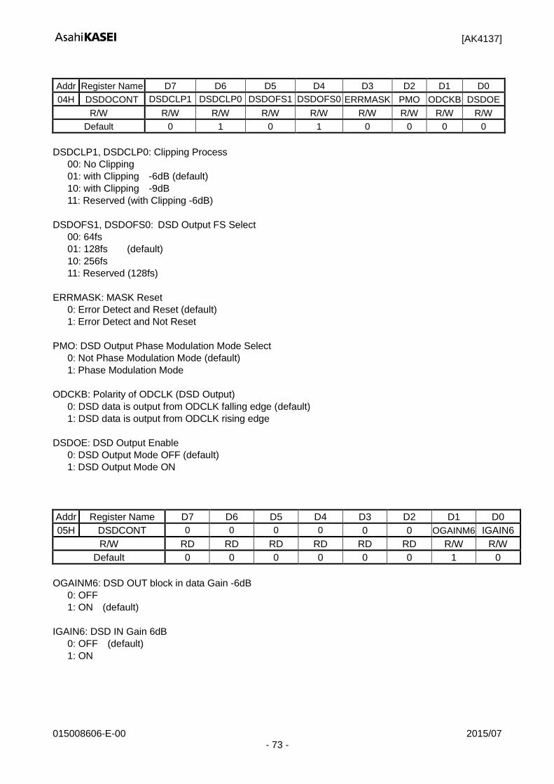
[AK4137]
015008606-E-00 2015/07 - 73 -
Addr Register Name D7 D6 D5 D4 D3 D2 D1 D0
04H DSDOCONT DSDCLP1 DSDCLP0 DSDOFS1 DSDOFS0 ERRMASK PMO ODCKB DSDOE
R/W R/W R/W R/W R/W R/W R/W R/W R/W
Default 0 1 0 1 0 0 0 0
DSDCLP1, DSDCLP0: Clipping Process
00: No Clipping
01: with Clipping -6dB (default)
10: with Clipping -9dB
11: Reserved (with Clipping -6dB)
DSDOFS1, DSDOFS0: DSD Output FS Select
00: 64fs
01: 128fs (default)
10: 256fs
11: Reserved (128fs)
ERRMASK: MASK Reset
0: Error Detect and Reset (default)
1: Error Detect and Not Reset
PMO: DSD Output Phase Modulation Mode Select
0: Not Phase Modulation Mode (default)
1: Phase Modulation Mode
ODCKB: Polarity of ODCLK (DSD Output)
0: DSD data is output from ODCLK falling edge (default)
1: DSD data is output from ODCLK rising edge
DSDOE: DSD Output Enable
0: DSD Output Mode OFF (default)
1: DSD Output Mode ON
Addr Register Name D7 D6 D5 D4 D3 D2 D1 D0
05H DSDCONT 0 0 0 0 0 0 OGAINM6 IGAIN6
R/W RD RD RD RD RD RD R/W R/W
Default 0 0 0 0 0 0 1 0
OGAINM6: DSD OUT block in data Gain -6dB
0: OFF
1: ON (default)
IGAIN6: DSD IN Gain 6dB
0: OFF (default)
1: ON
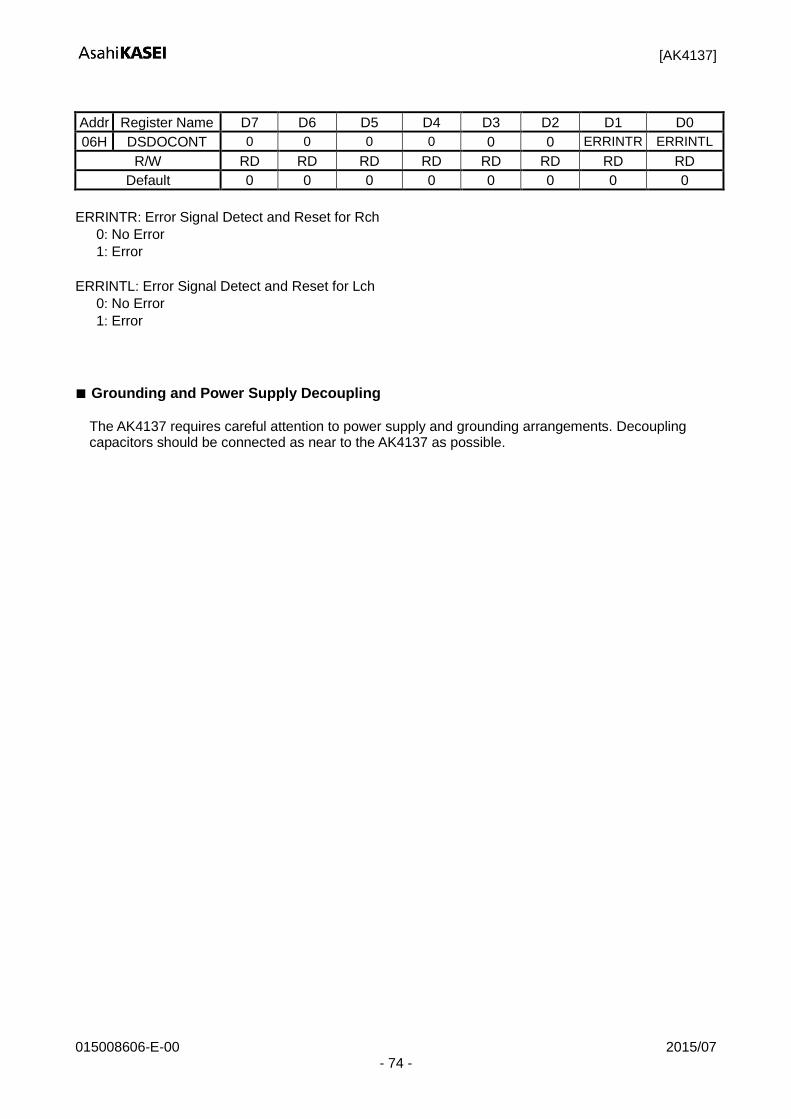
[AK4137]
015008606-E-00 2015/07 - 74 -
Addr Register Name D7 D6 D5 D4 D3 D2 D1 D0
06H DSDOCONT 0 0 0 0 0 0 ERRINTR ERRINTL
R/W RD RD RD RD RD RD RD RD
Default 0 0 0 0 0 0 0 0
ERRINTR: Error Signal Detect and Reset for Rch
0: No Error
1: Error
ERRINTL: Error Signal Detect and Reset for Lch
0: No Error
1: Error
Grounding and Power Supply Decoupling
The AK4137 requires careful attention to power supply and grounding arrangements. Decoupling capacitors should be connected as near to the AK4137 as possible.
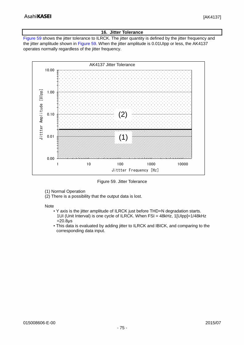
[AK4137]
015008606-E-00 2015/07 - 75 -
16. Jitter Tolerance
Figure 59 shows the jitter tolerance to ILRCK. The jitter quantity is defined by the jitter frequency and
the jitter amplitude shown in Figure 59. When the jitter amplitude is 0.01UIpp or less, the AK4137
operates normally regardless of the jitter frequency.
Figure 59. Jitter Tolerance
(1) Normal Operation (2) There is a possibility that the output data is lost. Note
Y axis is the jitter amplitude of ILRCK just before THD+N degradation starts. 1UI (Unit Interval) is one cycle of ILRCK. When FSI = 48kHz, 1[UIpp]=1/48kHz =20.8μs
This data is evaluated by adding jitter to ILRCK and IBICK, and comparing to the corresponding data input.
0.00
0.01
0.10
1.00
10.00
1 10 100 1000 10000 100000
Jittter Frequency [Hz]
Jittter Amplitude [UIpp]
(2)
(1)
AK4137 Jitter Tolerance
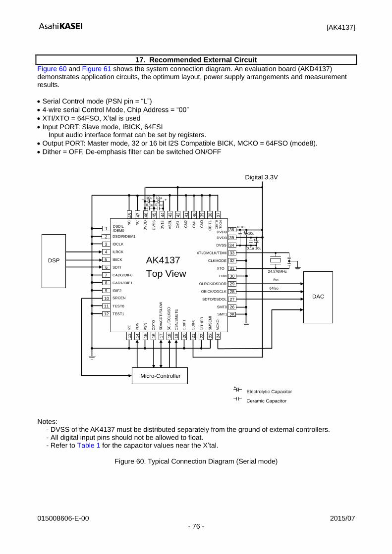
[AK4137]
015008606-E-00 2015/07 - 76 -
17. Recommended External Circuit
Figure 60 and Figure 61 shows the system connection diagram. An evaluation board (AKD4137) demonstrates application circuits, the optimum layout, power supply arrangements and measurement results.
Serial Control mode (PSN pin = “L”)
4-wire serial Control Mode, Chip Address = “00”
XTI/XTO = 64FSO, X’tal is used
Input PORT: Slave mode, IBICK, 64FSI Input audio interface format can be set by registers.
Output PORT: Master mode, 32 or 16 bit I2S Compatible BICK, MCKO = 64FSO (mode8).
Dither = OFF, De-emphasis filter can be switched ON/OFF
Ceramic Capacitor
+ Electrolytic Capacitor
Digital 3.3V
+
0.1u
10u
Micro-Controller
+ DSDIR/DEM1
NC
1
IDCLK
44
2
ILRCK
3
IBICK
4
SDTI
5
CAD0/IDIF0
6
CAD1/IDIF1
7
IDIF2
8
SRCEN
9
TEST0
10
TEST1
11
I2C
33
DVDD
13
14
15
16
17
19
20
21
22
PD
N
PS
N
CD
TO
SD
A/C
DT
I/S
LO
W
CS
N/S
MU
TE
OD
IF1
OD
IF0
DIT
HE
R
SM
SE
MI
MC
KO
32
DVSS
31
XTI/OMCLK/TDMI
30
CLKMODE
29
XTO
28
27
TDM N
26
OLRCK/DSDOR
25
OBICK/ODCLK
SDTO/DSDOL
SMT0
NC
43
DV
DD
42
DV
SS
41
DV
18
40
CM
3
39
CM
2
38
CM
1
37
CM
0
OB
IT1
DSDIL /DEM0
23
24
18
SC
L/C
CLK
/SD
SMT1
DVDD
34
35
36
48
47
46
45
VS
EL
OB
IT0
/TD
O4
12
Top View
DSP
0.1u
0.1u
10u
10u
+
DAC
64fso
fso
24.576MHz
AK4137
+ 0.1u
10u
Notes:
- DVSS of the AK4137 must be distributed separately from the ground of external controllers. - All digital input pins should not be allowed to float. - Refer to Table 1 for the capacitor values near the X’tal.
Figure 60. Typical Connection Diagram (Serial mode)
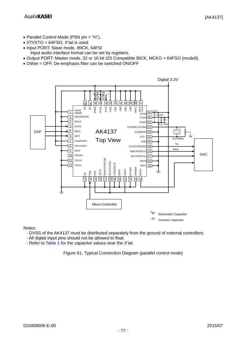
[AK4137]
015008606-E-00 2015/07 - 77 -
Parallel Control Mode (PSN pin = “H”).
XTI/XTO = 64FSO, X’tal is used
Input PORT: Slave mode, IBICK, 64FSI Input audio interface format can be set by registers.
Output PORT: Master mode, 32 or 16 bit I2S Compatible BICK, MCKO = 64FSO (mode8).
Dither = OFF, De-emphasis filter can be switched ON/OFF
Ceramic Capacitor
+ Electrolytic Capacitor
Digital 3.3V
+
0.1u
10u
Micro-Controller
+ DSDIR/DEM1
NC
1
IDCLK
44
2
ILRCK
3
IBICK
4
SDTI
5
CAD0/IDIF0
6
CAD1/IDIF1
7
IDIF2
8
SRCEN
9
TEST0
10
TEST1
11
I2C
33
DVDD
13
14
15
16
17
19
20
21
22
PD
N
PS
N
CD
TO
SD
A/C
DT
I/S
LO
W
CS
N/S
MU
TE
OD
IF1
OD
IF0
DIT
HE
R
SM
SE
MI
MC
KO
32
DVSS
31
XTI/OMCLK/TDMI
30
CLKMODE
29
XTO
28
27
TDM
26
OLRCK/DSDOR
25
OBICK/ODCLK
SDTO/DSDOL
SMT0
NC
43
DV
DD
42
DV
SS
41
DV
18
40
CM
3
39
CM
2
38
CM
1
37
CM
0
OB
IT1
DSDIL /DEM0
23
24
18
SC
L/C
CL
K/S
D
SMT1
DVDD
34
35
36
48
47
46
45
VS
EL
OB
IT0
/TD
O4
12
Top View
DSP
0.1u
0.1u
10u
10u
+
DAC
64fso
fso
24.576MHz
AK4137
0.1u
10u +
Notes:
- DVSS of the AK4137 must be distributed separately from the ground of external controllers. - All digital input pins should not be allowed to float. - Refer to Table 1 for the capacitor values near the X’tal.
Figure 61. Typical Connection Diagram (parallel control mode)
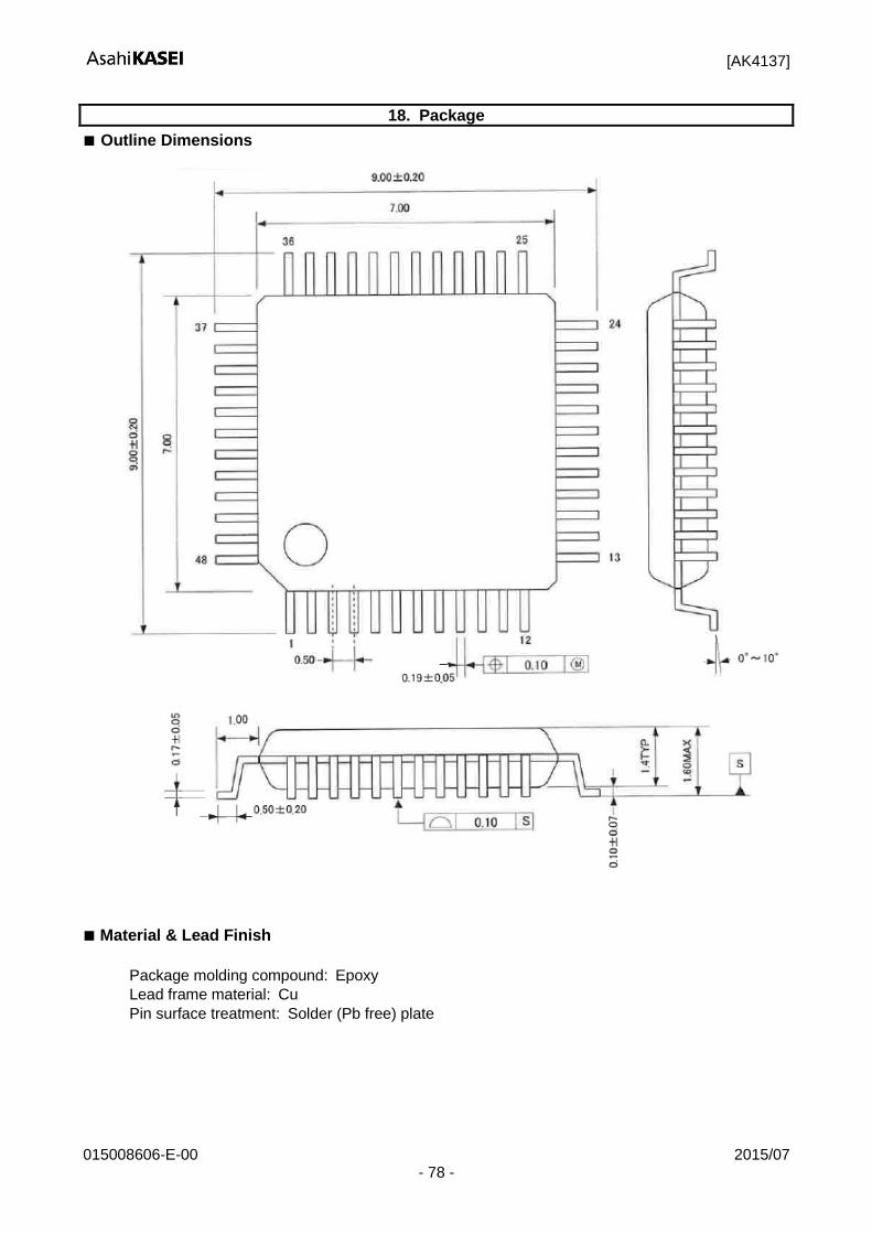
[AK4137]
015008606-E-00 2015/07 - 78 -
18. Package
Outline Dimensions
Material & Lead Finish
Package molding compound: Epoxy
Lead frame material: Cu
Pin surface treatment: Solder (Pb free) plate
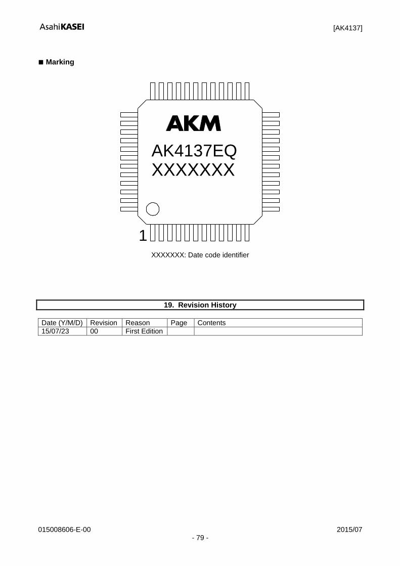
[AK4137]
015008606-E-00 2015/07 - 79 -
Marking
AK4137EQ XXXXXXX
1
XXXXXXX: Date code identifier
19. Revision History
Date (Y/M/D) Revision Reason Page Contents
15/07/23 00 First Edition
[AK4137]
015008606-E-00 2015/07 - 80 -
IMPORTANT NOTICE
0. Asahi Kasei Microdevices Corporation (“AKM”) reserves the right to make changes to the information contained in this document without notice. When you consider any use or application of AKM product stipulated in this document (“Product”), please make inquiries the sales office of AKM or authorized distributors as to current status of the Products.
1. All information included in this document are provided only to illustrate the operation and application examples of AKM Products. AKM neither makes warranties or representations with respect to the accuracy or completeness of the information contained in this document nor grants any license to any intellectual property rights or any other rights of AKM or any third party with respect to the information in this document. You are fully responsible for use of such information contained in this document in your product design or applications. AKM ASSUMES NO LIABILITY FOR ANY LOSSES INCURRED BY YOU OR THIRD PARTIES ARISING FROM THE USE OF SUCH INFORMATION IN YOUR PRODUCT DESIGN OR APPLICATIONS.
2. The Product is neither intended nor warranted for use in equipment or systems that require extraordinarily high levels of quality and/or reliability and/or a malfunction or failure of which may cause loss of human life, bodily injury, serious property damage or serious public impact, including but not limited to, equipment used in nuclear facilities, equipment used in the aerospace industry, medical equipment, equipment used for automobiles, trains, ships and other transportation, traffic signaling equipment, equipment used to control combustions or explosions, safety devices, elevators and escalators, devices related to electric power, and equipment used in finance-related fields. Do not use Product for the above use unless specifically agreed by AKM in writing.
3. Though AKM works continually to improve the Product’s quality and reliability, you are responsible for complying with safety standards and for providing adequate designs and safeguards for your hardware, software and systems which minimize risk and avoid situations in which a malfunction or failure of the Product could cause loss of human life, bodily injury or damage to property, including data loss or corruption.
4. Do not use or otherwise make available the Product or related technology or any information contained in this document for any military purposes, including without limitation, for the design, development, use, stockpiling or manufacturing of nuclear, chemical, or biological weapons or missile technology products (mass destruction weapons). When exporting the Products or related technology or any information contained in this document, you should comply with the applicable export control laws and regulations and follow the procedures required by such laws and regulations. The Products and related technology may not be used for or incorporated into any products or systems whose manufacture, use, or sale is prohibited under any applicable domestic or foreign laws or regulations.
5. Please contact AKM sales representative for details as to environmental matters such as the RoHS compatibility of the Product. Please use the Product in compliance with all applicable laws and regulations that regulate the inclusion or use of controlled substances, including without limitation, the EU RoHS Directive. AKM assumes no liability for damages or losses occurring as a result of noncompliance with applicable laws and regulations.
6. Resale of the Product with provisions different from the statement and/or technical features set forth in this document shall immediately void any warranty granted by AKM for the Product and shall not create or extend in any manner whatsoever, any liability of AKM.
7. This document may not be reproduced or duplicated, in any form, in whole or in part, without prior written consent of AKM.