
32-Bit Microprocessor
112
32-Bit Microprocessor Student Workbook 91577-00 Edition 4 |3091577000000^~
Transcript of 32-Bit Microprocessor
32-Bit Microprocessor
Student Workbook
91577-00 Edition 4 |3091577000000^~

FOURTH EDITION
Fourth Printing, June 2009
Copyright June, 2003 Lab-Volt Systems, Inc.
All rights reserved. No part of this publication may be reproduced, stored in a retrieval system, or transmitted in any form by any means, electronic, mechanical, photocopied, recorded, or otherwise, without prior written permission from Lab-Volt Systems, Inc.
Information in this document is subject to change without notice and does not represent a commitment on the part of Lab-Volt Systems, Inc. The Lab-Volt FACET® software and other materials described in this document are furnished under a license agreement or a nondisclosure agreement. The software may be used or copied only in accordance with the terms of the agreement.
ISBN 978-0-86657-219-4 Lab-Volt and FACET® logos are trademarks of Lab-Volt Systems, Inc. All other trademarks are the property of their respective owners. Other trademarks and trade names may be used in this document to refer to either the entity claiming the marks and names or their products. Lab-Volt System, Inc. disclaims any proprietary interest in trademarks and trade names other than its own.
Lab-Volt License Agreement By using the software in this package, you are agreeing to become bound by the terms of this License Agreement, Limited Warranty, and Disclaimer. This License Agreement constitutes the complete agreement between you and Lab-Volt. If you do not agree to the terms of this agreement, do not use the software. Promptly return the FACET Resources on Multimedia (CD-ROM) compact discs and all other materials that are part of Lab-Volt's FACET product within ten days to Lab-Volt for a full refund or credit. 1. License Grant. In consideration of payment of the license fee, which is part of the price you paid for this Lab-Volt product, Lab-Volt, as Licensor, grants to you, the Licensee, a nonexclusive, nontransferable license to use this copy of the CD-ROM software with the corresponding FACET Lab-Volt reserves all rights not expressly granted to the Licensee. 2. Ownership. As the Licensee, you own the physical media on which the CD-ROM is originally or subsequently recorded or fixed, but Lab-Volt retains title to and ownership of the software programs recorded on the original compact disc and any subsequent copies of the CD-ROM, regardless of the form or media in or on which the original and other copies may exist. This license is not a sale of the original software program of Lab-Volt's CD-ROM or any portion or copy of it. 3. Copy Restrictions. The CD-ROM software and the accompanying materials are copyrighted and contain proprietary information and trade secrets of Lab-Volt. Unauthorized copying of the CD-ROM even if modified, merged, or included with other software or with written materials is expressly forbidden. You may be held legally responsible for any infringement of Lab-Volt's intellectual property rights that is caused or encouraged by your failure to abide by the terms of this agreement. You may make copies of the CD-ROM solely for backup purposes provided the copyright notice is reproduced in its entirety on the backup copy. 4. Permitted Uses. This CD-ROM, Instructor's Guide, and all accompanying documentation is licensed to you, the Licensee, and may not be transferred to any third party for any length of time without the prior written consent of Lab-Volt. You may not modify, adapt, translate, reverse engineer, decompile, disassemble, or create derivative works based on the Lab-Volt product without the prior written permission of Lab-Volt. Written materials provided to you may not be modified, adapted, translated, or used to create derivative works without the prior written consent of Lab-Volt. 5. Termination. This agreement is effective until terminated. It will terminate automatically without notice from Lab-Volt if you fail to comply with any provisions contained herein. Upon termination you shall destroy the written materials, Lab-Volt's CD-ROM software, and all copies of them, in part or in whole, including modified copies, if any.
6. Registration. Lab-Volt may from time to time update the CD-ROM. Updates can be made available to you only if a properly signed registration card is filed with Lab-Volt or an authorized registration card recipient. 7. Miscellaneous. This agreement is governed by the laws of the State of New Jersey.
Limited Warranty and Disclaimer This CD-ROM software has been designed to assure correct operation when used in the manner and within the limits described in this Instructor's Guide. As a highly advanced software product, it is quite complex; thus, it is possible that if it is used in hardware configurations with characteristics other than those specified in this Instructor's Guide or in environments with nonspecified, unusual, or extensive other software products, problems may be encountered by a user. In such cases, Lab-Volt will make reasonable efforts to assist the user to properly operate the CD-ROM but without guaranteeing its proper performance in any hardware or software environment other than as described in this Instructor's Guide. This CD-ROM software is warranted to conform to the descriptions of its functions and performance as outlined in this Instructor's Guide. Upon proper notification and within a period of one year from the date of installation and/or customer acceptance, Lab-Volt, at its sole and exclusive option, will remedy any nonconformity or replace any defective compact disc free of charge. Any substantial revisions of this product, made for purposes of correcting software deficiencies within the warranty period, will be made available, also on a licensed basis, to registered owners free of charge. Warranty support for this product is limited, in all cases, to software errors. Errors caused by hardware malfunctions or the use of nonspecified hardware or other software are not covered. LICENSOR MAKES NO OTHER WARRANTIES OF ANY KIND CONCERNING THIS PRODUCT, INCLUDING WARRANTIES OR MERCHANTABILITY OR OF FITNESS FOR A PARTICULAR PURPOSE. LICENSOR DISCLAIMS ALL OBLIGATIONS AND LIABILITIES ON THE PART OF LICENSOR FOR DAMAGES, INCLUDING BUT NOT LIMITED TO SPECIAL OR CONSEQUENTIAL DAMAGES ARISING OUT OF OR IN CONNECTION WITH THE USE OF THE SOFTWARE PRODUCT LICENSED UNDER THIS AGREEMENT. Questions concerning this agreement and warranty and all requests for product repairs should be directed to the Lab-Volt field representative in your area. LAB-VOLT SYSTEMS, INC. P.O. Box 686 Farmingdale, NJ 07727 Attention: Program Development Phone: (732) 938-2000 or (800) LAB-VOLT Fax: (732) 774-8573 Technical Support: (800) 522-4436 Technical Support E-Mail: [email protected]
i
THIS PAGE IS SUPPOSE TO BE BLANK
Table of Contents
Unit 1 – Trainer Familiarization ..................................................................................................1
Exercise 1 – Introduction to the Trainer .....................................................................................5
Exercise 2 – Operating the Trainer .............................................................................................8
Unit 2 – Bus Operations ..............................................................................................................11
Exercise 1 – Bus States .............................................................................................................15
Exercise 2 – 32-Bit Bus Transfers ............................................................................................17
Exercise 3 – Read and Write Cycles .........................................................................................19
Exercise 4 – CPU Initialization.................................................................................................21
Unit 3 – Memory Interfacing ......................................................................................................23
Exercise 1 – Memory Control Signals ......................................................................................28
Exercise 2 – Memory Address Decoding..................................................................................30
Exercise 3 – Memory Data Transfers........................................................................................32
Unit 4 – I/O Interfacing ...............................................................................................................35
Exercise 1 – DAC and ADC Ports ............................................................................................38
Exercise 2 – PPI and Keypad Interface.....................................................................................40
Exercise 3 – Display and Serial Port.........................................................................................42
Unit 5 – Interrupt Processing......................................................................................................45
Exercise 1 – Non-maskable Interrupts ......................................................................................53
Exercise 2 – Maskable Interrupts..............................................................................................55
Exercise 3 – Exceptions ............................................................................................................58
Unit 6 – Programming: Addressing Modes ...............................................................................61
Exercise 1 – Immediate and Register Addressing Modes.........................................................68
Exercise 2 – Memory Addressing Modes - I ............................................................................70
Exercise 3 – Memory Addressing Modes - II ...........................................................................72
Unit 7 – Programming: 80386 Instructions ...............................................................................75
Exercise 1 – Instruction Formats - I ..........................................................................................78
Exercise 2 – Instruction Formats - II.........................................................................................80
Exercise 3 – Using the 80386 CPU Instructions - I ..................................................................82
Exercise 4 – Using the 80386 CPU Instructions - II.................................................................84

ii
Unit 8 – Troubleshooting.............................................................................................................87
Exercise 1 – Troubleshooting Basics ........................................................................................89
Exercise 2 – 32-Bit Microprocessor Troubleshooting ..............................................................90
Unit 9 – Microprocessor Applications (Optional).....................................................................91
Exercise 1 – Application Board Familiarization.......................................................................96
Exercise 2 – DC Motor Control ................................................................................................98
Exercise 3 – Temperature Control ..........................................................................................100
Appendix A – Safety ................................................................................................................. A-ii
iii
Introduction
This Student Workbook provides a unit-by-unit outline of the Fault Assisted Circuits for Electronics Training (FACET) curriculum. The following information is included together with space to take notes as you move through the curriculum. The unit objective Unit fundamentals A list of new terms and words for the unit Equipment required for the unit The exercise objectives Exercise discussion Exercise notes The Appendix includes safety information.

iv
THIS
32-Bit Microprocessor Unit 1 – Trainer Familiarization
1
UNIT 1 – TRAINER FAMILIARIZATION
UNIT OBJECTIVE Upon completion of this unit, you will be able to locate and describe the various components on your circuit board, and demonstrate basic trainer functions.
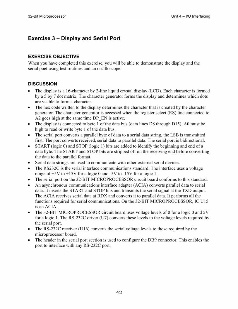
UNIT FUNDAMENTALS Microprocessors have changed virtually every facet of our daily lives. They can be found in office, industrial, and personal computers, as well as scientific and medical instrumentation. Even the car you drive may have on-board microprocessors to monitor and control some of the engine and braking functions.
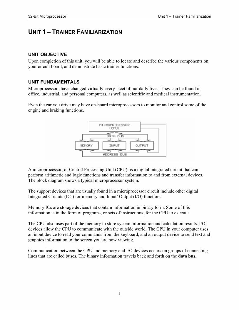
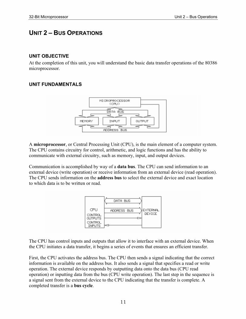
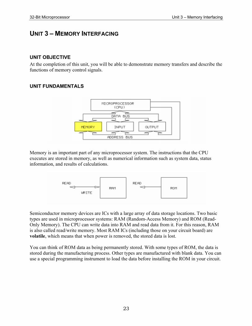
A microprocessor, or Central Processing Unit (CPU), is a digital integrated circuit that can perform arithmetic and logic functions and transfer information to and from external devices. The block diagram shows a typical microprocessor system. The support devices that are usually found in a microprocessor circuit include other digital Integrated Circuits (ICs) for memory and Input/ Output (I/O) functions. Memory ICs are storage devices that contain information in binary form. Some of this information is in the form of programs, or sets of instructions, for the CPU to execute. The CPU also uses part of the memory to store system information and calculation results. I/O devices allow the CPU to communicate with the outside world. The CPU in your computer uses an input device to read your commands from the keyboard, and an output device to send text and graphics information to the screen you are now viewing. Communication between the CPU and memory and I/O devices occurs on groups of connecting lines that are called buses. The binary information travels back and forth on the data bus.
32-Bit Microprocessor Unit 1 – Trainer Familiarization
2
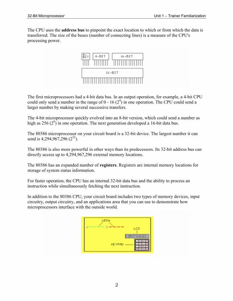
The CPU uses the address bus to pinpoint the exact location to which or from which the data is transferred. The size of the buses (number of connecting lines) is a measure of the CPU's processing power.
The first microprocessors had a 4-bit data bus. In an output operation, for example, a 4-bit CPU could only send a number in the range of 0 - 16 (24) in one operation. The CPU could send a larger number by making several successive transfers. The 4-bit microprocessor quickly evolved into an 8-bit version, which could send a number as high as 256 (28) in one operation. The next generation developed a 16-bit data bus. The 80386 microprocessor on your circuit board is a 32-bit device. The largest number it can send is 4,294,967,296 (232). The 80386 is also more powerful in other ways than its predecessors. Its 32-bit address bus can directly access up to 4,294,967,296 external memory locations. The 80386 has an expanded number of registers. Registers are internal memory locations for storage of system status information. For faster operation, the CPU has an internal 32-bit data bus and the ability to process an instruction while simultaneously fetching the next instruction. In addition to the 80386 CPU, your circuit board includes two types of memory devices, input circuitry, output circuitry, and an applications area that you can use to demonstrate how microprocessors interface with the outside world.
32-Bit Microprocessor Unit 1 – Trainer Familiarization
3
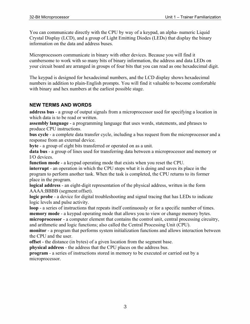
You can communicate directly with the CPU by way of a keypad, an alpha- numeric Liquid Crystal Display (LCD), and a group of Light Emitting Diodes (LEDs) that display the binary information on the data and address buses. Microprocessors communicate in binary with other devices. Because you will find it cumbersome to work with so many bits of binary information, the address and data LEDs on your circuit board are arranged in groups of four bits that you can read as one hexadecimal digit. The keypad is designed for hexadecimal numbers, and the LCD display shows hexadecimal numbers in addition to plain-English prompts. You will find it valuable to become comfortable with binary and hex numbers at the earliest possible stage.
NEW TERMS AND WORDS address bus - a group of output signals from a microprocessor used for specifying a location in which data is to be read or written. assembly language - a programming language that uses words, statements, and phrases to produce CPU instructions. bus cycle - a complete data transfer cycle, including a bus request from the microprocessor and a response from an external device. byte - a group of eight bits transferred or operated on as a unit. data bus - a group of lines used for transferring data between a microprocessor and memory or I/O devices. function mode - a keypad operating mode that exists when you reset the CPU. interrupt - an operation in which the CPU stops what it is doing and saves its place in the program to perform another task. When the task is completed, the CPU returns to its former place in the program. logical address - an eight-digit representation of the physical address, written in the form AAAA:BBBB (segment:offset). logic probe - a device for digital troubleshooting and signal tracing that has LEDs to indicate logic levels and pulse activity. loop - a series of instructions that repeats itself continuously or for a specific number of times. memory mode - a keypad operating mode that allows you to view or change memory bytes. microprocessor - a computer element that contains the control unit, central processing circuitry, and arithmetic and logic functions; also called the Central Processing Unit (CPU). monitor - a program that performs system initialization functions and allows interaction between the CPU and the user. offset - the distance (in bytes) of a given location from the segment base. physical address - the address that the CPU places on the address bus. program - a series of instructions stored in memory to be executed or carried out by a microprocessor.
32-Bit Microprocessor Unit 1 – Trainer Familiarization
4
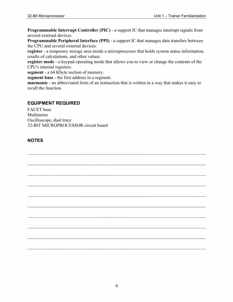
Programmable Interrupt Controller (PIC) - a support IC that manages interrupt signals from several external devices. Programmable Peripheral Interface (PPI) - a support IC that manages data transfers between the CPU and several external devices. register - a temporary storage area inside a microprocessor that holds system status information, results of calculations, and other values. register mode - a keypad operating mode that allows you to view or change the contents of the CPU's internal registers. segment - a 64 Kbyte section of memory. segment base - the first address in a segment. mnemonic - an abbreviated form of an instruction that is written in a way that makes it easy to recall the function.
EQUIPMENT REQUIRED FACET base Multimeter Oscilloscope, dual trace 32-BIT MICROPROCESSOR circuit board
NOTES ______________________________________________________________________________ ______________________________________________________________________________ ______________________________________________________________________________ ______________________________________________________________________________ ______________________________________________________________________________ ______________________________________________________________________________ ______________________________________________________________________________ ______________________________________________________________________________ ______________________________________________________________________________ ______________________________________________________________________________
32-Bit Microprocessor Unit 1 – Trainer Familiarization
5
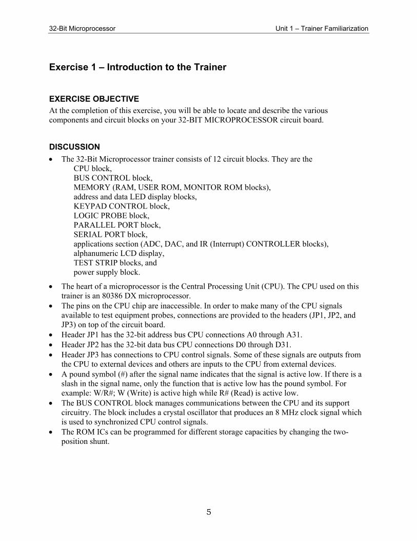
Exercise 1 – Introduction to the Trainer
EXERCISE OBJECTIVE At the completion of this exercise, you will be able to locate and describe the various components and circuit blocks on your 32-BIT MICROPROCESSOR circuit board.
DISCUSSION
The 32-Bit Microprocessor trainer consists of 12 circuit blocks. They are the CPU block, BUS CONTROL block, MEMORY (RAM, USER ROM, MONITOR ROM blocks), address and data LED display blocks, KEYPAD CONTROL block, LOGIC PROBE block, PARALLEL PORT block, SERIAL PORT block, applications section (ADC, DAC, and IR (Interrupt) CONTROLLER blocks), alphanumeric LCD display, TEST STRIP blocks, and power supply block.
The heart of a microprocessor is the Central Processing Unit (CPU). The CPU used on this trainer is an 80386 DX microprocessor.
The pins on the CPU chip are inaccessible. In order to make many of the CPU signals available to test equipment probes, connections are provided to the headers (JP1, JP2, and JP3) on top of the circuit board.
Header JP1 has the 32-bit address bus CPU connections A0 through A31. Header JP2 has the 32-bit data bus CPU connections D0 through D31. Header JP3 has connections to CPU control signals. Some of these signals are outputs from
the CPU to external devices and others are inputs to the CPU from external devices. A pound symbol (#) after the signal name indicates that the signal is active low. If there is a
slash in the signal name, only the function that is active low has the pound symbol. For example: W/R#; W (Write) is active high while R# (Read) is active low.
The BUS CONTROL block manages communications between the CPU and its support circuitry. The block includes a crystal oscillator that produces an 8 MHz clock signal which is used to synchronized CPU control signals.
The ROM ICs can be programmed for different storage capacities by changing the two-position shunt.

32-Bit Microprocessor Unit 1 – Trainer Familiarization
6
The trainer is shipped without ICs and shunts in the USER ROM block. This block is used with memory chips that contain your own programs.
The MONITOR ROM block allows direct programming of the CPU and contains the monitor program. Input information is enter from the keypad and output information is displayed on the LCD display.
External SERIAL PORT connections are made using a 9-pin, D-type connector (JP2 on this circuit block). The interface is uses the RS232 standard.
The SERIAL PORT has a 24-pin header to allow I/O signals to be monitored and provide shunts to program operating configurations.
The PARALLEL PORT circuit block has an 82C55 IC which consists of three programmable 8-bit bidirectional ports. The 3-pin header selects operating modes: normal (NORM) or a special test (TEST) mode.
The 20-pin header (JP6) provides access for the connection of external devices or test equipment.
The ADC IN and DAC OUT signals are connected to the ADC and DAC blocks, respectively.
The application blocks (DAC, ADC, and IR CONTROLLER) allow the CPU to interface with external devices to measure and control analog values such as voltage, current, temperature, and speed.
The DAC IC converts an 8-bit binary number to an analog voltage in one of two ranges. The 3-pin header selects an output voltage range of 0-10 Vdc or 0-2.56 Vdc. A shunt allows the selection of either unipolar or bipolar operation.
The ADC IC accepts an external analog signal and converts it to a proportional 8-bit binary value.
The IR CONTROLLER circuit block manages eight interrupt signals using the 82C59 Programmable Interrupt Controller (PIC). The PIC can be programmed for different operating modes and can establish a priority sequence for the interrupt signals. The 16-pin header allows access to IR0 through IR7 and allows shunts to be used to connect one of the top pins to the interrupt input directly below.
The POWER SUPPLY circuit block delivers a filtered and regulated 5 Vdc to all the of the circuit blocks. The supply will automatically shut down when overloaded.
The 32-BIT MICROPROCESSOR trainer can operate independently of the base unit when connected to an external 9 Vdc/750 mA power supply.
Manual controls include: 1. INTENSITY potentiometer to control the intensity of the LCD display 2. RESET switch 3. SINGLE CYCLE block consists of two switches. One indicates the mode of operation;
ON for STEP mode and OFF for RUN mode. The pushbutton switch allows the CPU to execute one STEP each time the switch is depressed.
4. HALT pushbutton stops CPU operation and allows you to step through a program one complete instruction at a time. (An instruction could consist of 1 to 14 bus cycles.) CPU registers can be viewed and/or changed in this mode of operation.
32-Bit Microprocessor Unit 1 – Trainer Familiarization
7
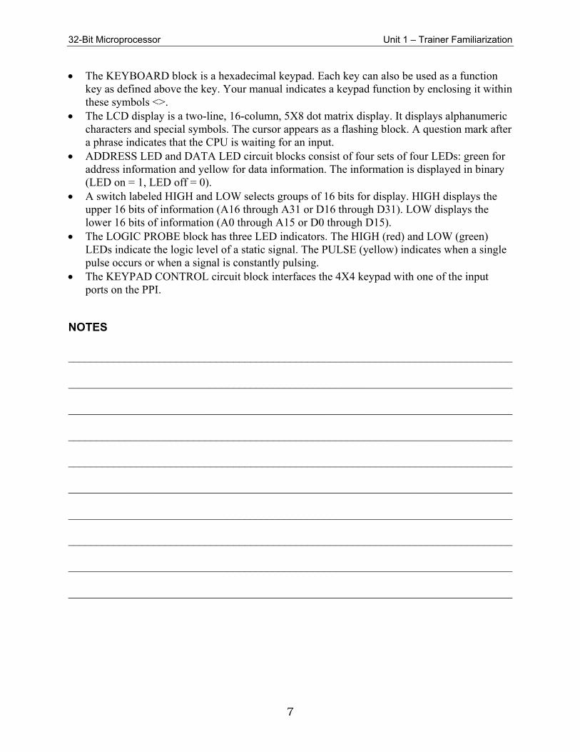
The KEYBOARD block is a hexadecimal keypad. Each key can also be used as a function key as defined above the key. Your manual indicates a keypad function by enclosing it within these symbols <>.
The LCD display is a two-line, 16-column, 5X8 dot matrix display. It displays alphanumeric characters and special symbols. The cursor appears as a flashing block. A question mark after a phrase indicates that the CPU is waiting for an input.
ADDRESS LED and DATA LED circuit blocks consist of four sets of four LEDs: green for address information and yellow for data information. The information is displayed in binary (LED on = 1, LED off = 0).
A switch labeled HIGH and LOW selects groups of 16 bits for display. HIGH displays the upper 16 bits of information (A16 through A31 or D16 through D31). LOW displays the lower 16 bits of information (A0 through A15 or D0 through D15).
The LOGIC PROBE block has three LED indicators. The HIGH (red) and LOW (green) LEDs indicate the logic level of a static signal. The PULSE (yellow) indicates when a single pulse occurs or when a signal is constantly pulsing.
The KEYPAD CONTROL circuit block interfaces the 4X4 keypad with one of the input ports on the PPI.
NOTES ______________________________________________________________________________ ______________________________________________________________________________ ______________________________________________________________________________ ______________________________________________________________________________ ______________________________________________________________________________ ______________________________________________________________________________ ______________________________________________________________________________ ______________________________________________________________________________ ______________________________________________________________________________ ______________________________________________________________________________

32-Bit Microprocessor Unit 1 – Trainer Familiarization
8
Exercise 2 – Operating the Trainer
EXERCISE OBJECTIVE At the completion of this exercise, you will be able to perform the basic keypad functions of the 32-BIT MICROPROCESSOR circuit board. You will verify your results by reading the data and prompts on the LCD display.
DISCUSSION
The 80386 CPU has two basic operating modes: real mode and protected mode. The real mode accommodates programs written for an earlier microprocessor series (the 8086
family). This series had only 20 address lines, limiting the amount of addressable memory space.
Whenever a reset occurs, the 80386 CPU is in real mode and has an address range of 1 Mbyte, which requires 5 hexadecimal digits.
In the protected mode some programs are not given access to certain (protected) memory areas.
The 32-BIT MICROPROCESSOR circuit board’s monitor resides in the first 1 Mbyte of memory and can operate in the real mode.
Each memory location has a unique physical address. The physical address is the value that the CPU places on the address bus to select a memory location.
Another way to specify a memory location is by the logical address. The logical address is composed of a segment and an offset, each consists of four hexadecimal digits separated from each other by a colon (AAAA:BBBB).
A segment is a 64-kilobyte section of memory: it is the first four digits, and is called the segment base.
The offset is the distance (in bytes) the memory location is from its section base. The offset is represented by the second set of four digits.
A physical address may have many equivalent logical addresses. To convert a logical address to a physical address, shift the segment base four bits to the left. In hexadecimal, this is equivalent to multiplying by 16, or simply adding a zero onto the right side of the address.
The keyboard provides a direct interface to the CPU. At start up the LCDs display the message “Lab-Volt 32 bit Proc. Trainer” and waits for an input.
This is the function mode and only the REG, GO, READ, and STEP function keys are active. The GO function causes the CPU to jump to a memory location that must be entered. The READ function provides the ability to view or change information stored in memory.
The logical address is entered and the computer displays the starting physical address and eight pairs of hex digits which represent the data bytes stored in that memory segment.
The FWD and BACK keys move the cursor one byte at a time in either direction. The FFWD and FBACK keys move the cursor eight bytes at a time in either direction.
32-Bit Microprocessor Unit 1 – Trainer Familiarization
9
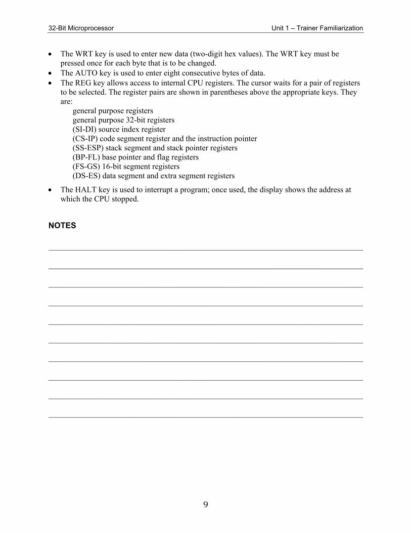
The WRT key is used to enter new data (two-digit hex values). The WRT key must be pressed once for each byte that is to be changed.
The AUTO key is used to enter eight consecutive bytes of data. The REG key allows access to internal CPU registers. The cursor waits for a pair of registers
to be selected. The register pairs are shown in parentheses above the appropriate keys. They are:
general purpose registers general purpose 32-bit registers (SI-DI) source index register (CS-IP) code segment register and the instruction pointer (SS-ESP) stack segment and stack pointer registers (BP-FL) base pointer and flag registers (FS-GS) 16-bit segment registers (DS-ES) data segment and extra segment registers
The HALT key is used to interrupt a program; once used, the display shows the address at which the CPU stopped.
NOTES ______________________________________________________________________________ ______________________________________________________________________________ ______________________________________________________________________________ ______________________________________________________________________________ ______________________________________________________________________________ ______________________________________________________________________________ ______________________________________________________________________________ ______________________________________________________________________________ ______________________________________________________________________________ ______________________________________________________________________________

32-Bit Microprocessor Unit 1 – Trainer Familiarization
10
32-Bit Microprocessor Unit 2 – Bus Operations
11
UNIT 2 – BUS OPERATIONS
UNIT OBJECTIVE At the completion of this unit, you will understand the basic data transfer operations of the 80386 microprocessor.
UNIT FUNDAMENTALS
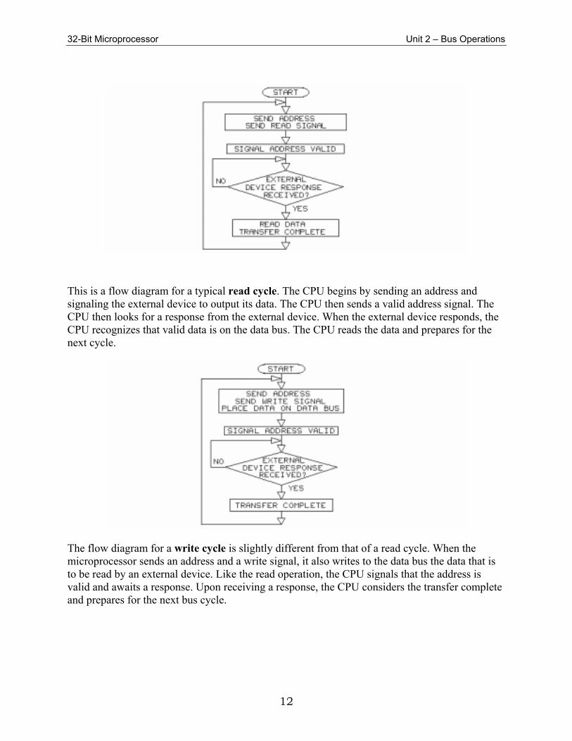
A microprocessor, or Central Processing Unit (CPU), is the main element of a computer system. The CPU contains circuitry for control, arithmetic, and logic functions and has the ability to communicate with external circuitry, such as memory, input, and output devices. Communication is accomplished by way of a data bus. The CPU can send information to an external device (write operation) or receive information from an external device (read operation). The CPU sends information on the address bus to select the external device and exact location to which data is to be written or read.
The CPU has control inputs and outputs that allow it to interface with an external device. When the CPU initiates a data transfer, it begins a series of events that ensures an efficient transfer. First, the CPU activates the address bus. The CPU then sends a signal indicating that the correct information is available on the address bus. It also sends a signal that specifies a read or write operation. The external device responds by outputting data onto the data bus (CPU read operation) or inputting data from the bus (CPU write operation). The last step in the sequence is a signal sent from the external device to the CPU indicating that the transfer is complete. A completed transfer is a bus cycle.
32-Bit Microprocessor Unit 2 – Bus Operations
12
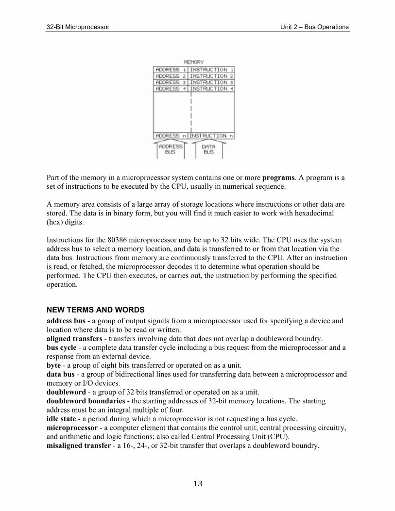
This is a flow diagram for a typical read cycle. The CPU begins by sending an address and signaling the external device to output its data. The CPU then sends a valid address signal. The CPU then looks for a response from the external device. When the external device responds, the CPU recognizes that valid data is on the data bus. The CPU reads the data and prepares for the next cycle.
The flow diagram for a write cycle is slightly different from that of a read cycle. When the microprocessor sends an address and a write signal, it also writes to the data bus the data that is to be read by an external device. Like the read operation, the CPU signals that the address is valid and awaits a response. Upon receiving a response, the CPU considers the transfer complete and prepares for the next bus cycle.
32-Bit Microprocessor Unit 2 – Bus Operations
13
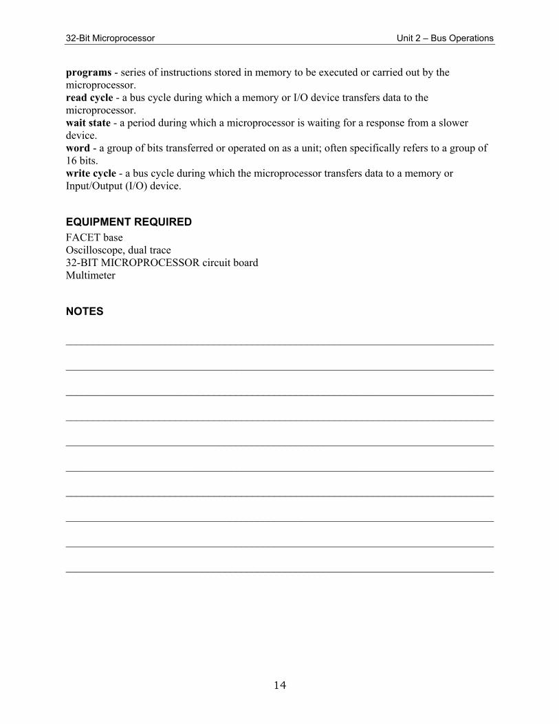
Part of the memory in a microprocessor system contains one or more programs. A program is a set of instructions to be executed by the CPU, usually in numerical sequence. A memory area consists of a large array of storage locations where instructions or other data are stored. The data is in binary form, but you will find it much easier to work with hexadecimal (hex) digits. Instructions for the 80386 microprocessor may be up to 32 bits wide. The CPU uses the system address bus to select a memory location, and data is transferred to or from that location via the data bus. Instructions from memory are continuously transferred to the CPU. After an instruction is read, or fetched, the microprocessor decodes it to determine what operation should be performed. The CPU then executes, or carries out, the instruction by performing the specified operation.
NEW TERMS AND WORDS address bus - a group of output signals from a microprocessor used for specifying a device and location where data is to be read or written. aligned transfers - transfers involving data that does not overlap a doubleword boundry. bus cycle - a complete data transfer cycle including a bus request from the microprocessor and a response from an external device. byte - a group of eight bits transferred or operated on as a unit. data bus - a group of bidirectional lines used for transferring data between a microprocessor and memory or I/O devices. doubleword - a group of 32 bits transferred or operated on as a unit. doubleword boundaries - the starting addresses of 32-bit memory locations. The starting address must be an integral multiple of four. idle state - a period during which a microprocessor is not requesting a bus cycle. microprocessor - a computer element that contains the control unit, central processing circuitry, and arithmetic and logic functions; also called Central Processing Unit (CPU). misaligned transfer - a 16-, 24-, or 32-bit transfer that overlaps a doubleword boundry.
32-Bit Microprocessor Unit 2 – Bus Operations
14
programs - series of instructions stored in memory to be executed or carried out by the microprocessor. read cycle - a bus cycle during which a memory or I/O device transfers data to the microprocessor. wait state - a period during which a microprocessor is waiting for a response from a slower device. word - a group of bits transferred or operated on as a unit; often specifically refers to a group of 16 bits. write cycle - a bus cycle during which the microprocessor transfers data to a memory or Input/Output (I/O) device.
EQUIPMENT REQUIRED FACET base Oscilloscope, dual trace 32-BIT MICROPROCESSOR circuit board Multimeter
NOTES ______________________________________________________________________________ ______________________________________________________________________________ ______________________________________________________________________________ ______________________________________________________________________________ ______________________________________________________________________________ ______________________________________________________________________________ ______________________________________________________________________________ ______________________________________________________________________________ ______________________________________________________________________________ ______________________________________________________________________________
32-Bit Microprocessor Unit 2 – Bus Operations
15
Exercise 1 – Bus States
EXERCISE OBJECTIVE When you have completed this exercise, you will understand the bus states that allow the 80386 microprocessor to communicate with memory and Input/Output (I/O) devices. You will verify your results by using an oscilloscope and by loading and executing a simple program in the 32-BIT MICROPROCESSOR circuit board.
DISCUSSION
The signal clock (CLK2) is used to establish a timing relationship between the various signals in an 80386 microprocessor system.
A second clock signal (CLK) is internally derived by the CPU from CLK2, and is half the frequency of CLK2.
All internal and external CPU operations can be referenced to the CLK signal. A typical bus cycle consists of two CLK cycles called bus states T1 and T2. The CPU requests a data transfer from an external device during the T1 state. The external device transfers the data during the T2 state. The 80386 I/O lines consist of five bus status outputs and three bus control inputs which are
used for communicating between the CPU and memory or I/O. The bus status outputs are ADS#, W/R#, M/IO#, D/C#, and LOCK#. The bus control inputs
are RDY#, NA#, and BS16#. This exercise focuses on the functions of the status output ADS# (ADdress Status line) and
the control input RDY# (ReaDY line). The ADS# line is the CPU control line that initiates every bus cycle, and tells an external
device that valid data is present on the address bus. The actions of the ADS# and the address lines are referenced to the CLK signal. The microprocessor activates ADS# when valid data is on the address bus. The ADS# line is
active for the T1 state, only. The RDY# input signal is an external device’s signal to the CPU that it recognizes a bus
request and has responded. An active RDY# input allows the CPU to terminate the bus cycle at the end of T2.
The CPU looks at the RDY# line at the end of the T2 cycle; therefore the value of the RDY# line may indicate a “don’t care” condition until that time.
Once the RDY# has been read as valid, the CPU reads the data that has been placed on the bus by the external device and terminates the cycle.
The CPU remains in a wait state when the sampled RDY# signal is inactive. The CPU executes T2 states until RDY# becomes active. Once RDY# becomes active the CPU exits the wait state and proceeds to the next bus cycle.
32-Bit Microprocessor Unit 2 – Bus Operations
16
Wait states allow microprocessors to communicate with devices that are slower than the CPU.
At times when the CPU is not ready to fetch data it does not activate ADS# to start a bus cycle. The state that follows the last bus cycle is an idle state (Ti).
The idle state continues until the next bus cycle requiring a data transfer occurs. The idle state (Ti) terminates when the CPU requests a data transfer by activating ADS#.
A state diagram can be used to illustrate the transitions between the different microprocessor states.
NOTES ______________________________________________________________________________ ______________________________________________________________________________ ______________________________________________________________________________ ______________________________________________________________________________ ______________________________________________________________________________ ______________________________________________________________________________ ______________________________________________________________________________ ______________________________________________________________________________ ______________________________________________________________________________ ______________________________________________________________________________
32-Bit Microprocessor Unit 2 – Bus Operations
17
Exercise 2 – 32-Bit Bus Transfers
EXERCISE OBJECTIVE When you have completed this exercise, you will be able to demonstrate data transfers on the 32-BIT MICROPROCESSOR circuit board. You will verify your results with an oscilloscope.
DISCUSSION
There are several other signals that are required to fully define the data transfer process of an 80836 microprocessor system. They include the bus status outputs ADS#, W/R#, M/IO#, D/C# and LOCK#, the bus control inputs RDY#, NA# and BS16#, and the byte enable outputs BE0#, BE1#, BE2#, and BE3#.
In this exercise the Byte Enable outputs are examined. A 32-bit data bus can transfer data in groups of 8, 16, 24, or 32 bits at a time. A group of 8
bits is called a byte and has a hexadecimal range of 00-FFH, or 0-25610. A group of 16 bites is a word. The hexadecimal range for a word is 0000-FFFFH, which is
equivalent to 0-65,53610 (64K). A group of 32 bits is a doubleword. The hexadecimal range of a doubleword is 0000 0000-
FFFF FFFFH, or 0-4,294,067,29610. There is no special name for a 24-bit group. The four bytes of the 32-bit data group are designated byte 0 through byte 3. Byte 0 (D0
through D7) is the least significant bit (LSB) and byte 3 (D24 through D31) is the most significant bit (MSB).
Depending on the instruction being executed by the CPU, some, or all of the four bytes may be required for bus transfer.
The byte enable output lines notify external devices on the condition of each data byte. BE0# corresponds to byte 0, BE1# corresponds to byte 1, BE2# corresponds to byte 2, and BE3# corresponds to byte 3.
The CPU uses the byte enable outputs with the address bus to select one or more bytes for data transfer.
Address lines A2 through A31 are used to select a 32-bit memory location. A0 and A1 are used to internally generate the four byte-enable lines. The byte-enable lines are used to select one or more bytes within that location. The data in the selected areas is then transferred onto the data bus.
If more than one byte is to be transferred, the bytes must be contiguous. The upper and lower limits of a 32-bit location are the doubleword boundaries. Data to be
transferred may be entirely within the doubleword boundary or may overlap one of them. Data transfers which involve bytes within the doubleword boundaries are called aligned
transfers. This type of data is at one doubleword address, and since one address in sent for each bus cycle the data can be transferred in one bus cycle.
32-Bit Microprocessor Unit 2 – Bus Operations
18
Data transfers which involve bytes which overlap the doubleword boundaries are called misaligned transfers. The CPU transfers data from the higher address and then from the lower address. The CPU requires two bus cycles to complete a misaligned transfer.
The byte enable lines are considered part of the addressing system. The remaining signals involved in a memory data transfer are:
1. (Write/Read#) whose output is high when the CPU writes data to memory or I/O, and low when it reads data from memory or I/O.
2. M/IO# (Memory/Input-Output#) whose output is high when data is transferred between the CPU and memory, and low when the transfer is between the CPU and I/O devices.
3. (Data Control#) has a high output for data transfers and a low output for instruction (control) transfers.
4. BS16# is an input which is used by a 16-bit device to signal the CPU to convert to its 16-bit mode.
NOTES ______________________________________________________________________________ ______________________________________________________________________________ ______________________________________________________________________________ ______________________________________________________________________________ ______________________________________________________________________________ ______________________________________________________________________________ ______________________________________________________________________________ ______________________________________________________________________________ ______________________________________________________________________________ ______________________________________________________________________________
32-Bit Microprocessor Unit 2 – Bus Operations
19
Exercise 3 – Read and Write Cycles
EXERCISE OBJECTIVE When you have completed this exercise, you will understand the functions of CPU read cycles and write cycles. You will verify your results with an oscilloscope.
DISCUSSION
In a read cycle, data is transferred from memory or I/O to the CPU. In a write cycle, data is transferred from the CPU to memory or I/O. The W/R# (Write/Read#) status output determines the type of cycle being executed. When an external device recognizes a valid address and read command (W/R# low), it
responds by placing its data on the data bus and driving RDY# low before T2 ends. The CPU then reads the data and terminates the read cycle.
In a write cycle, the CPU issues a low ADS# pulse and a valid address. Midway through the T1 cycle, the CPU writes its data to the data bus so an external device can read the data. The information remains on the data bus until midway through T1 of the next bus cycle.
There are different types of read and write cycles. The type of cycle will depend on the status of the M/IO# and D/C# lines, as well as the W/R# line.
When M/IO# is low an I/O cycle is executed. D/C# is always high for an I/O cycle since instructions are always fetched from memory during an I/O cycle. The W/R# line determines whether the I/O cycle is a data read or a data write function.
There are two types of memory read cycles: memory code read and memory data read. A memory code read occurs when W/R# is low and the CPU fetches an instruction. A memory data read occurs when the CPU reads data from memory.
The D/C# signal determines if a memory read cycle is a memory code read (D/C# low) of a memory data read (D/C# high).

32-Bit Microprocessor Unit 2 – Bus Operations
20
NOTES ______________________________________________________________________________ ______________________________________________________________________________ ______________________________________________________________________________ ______________________________________________________________________________ ______________________________________________________________________________ ______________________________________________________________________________ ______________________________________________________________________________ ______________________________________________________________________________ ______________________________________________________________________________ ______________________________________________________________________________
32-Bit Microprocessor Unit 2 – Bus Operations
21
Exercise 4 – CPU Initialization
EXERCISE OBJECTIVE When you have completed this exercise, you will be able to describe the reset state and initialization procedure of the 80386 microprocessor.
DISCUSSION
Capacitor C40 and resistor R42 are connected to the inverter input to form a power-up reset circuit.
When power is first applied, the capacitor maintains a low logic level at the inverter (RES#) which initiates a reset cycle. The capacitor charges through R42; when the threshold voltage of the inverter input is reached, the output RES goes high and the reset cycle is terminated.
While the circuit board is powered up, a reset can be generated by pressing the RESET switch. Closing this switch discharges the capacitor through R40. When the switch opens, the capacitor is charged through R42, and RES goes high terminating the reset cycle.
The RES signal is connected to a programmable logic device (PLD). In this circuit, the RES signal is gated with CLK2 to synchronize a power-up reset or a push button reset with the CPU clock. The resulting output, RESET, is connected to the CPU and other devices that require the signal.
The reset condition causes the CPU to suspend all bus activity and set the outputs shown below to the levels indicated.
D/C#, ADS#, A0-A31 high W/R#, M/IO#, BE0#-BE3# low D0-D31 tristate
If the CPU is reset in its RUN mode, you can not determine if the failure due to a circuit fault occurred during the reset or afterward.
Reset the computer in the SINGLE CYCLE mode to determine if a failure occurs during reset. This mode allows you to examine signals statically and compare their levels.
The steps the CPU executes after reset are: 1. fetch an instruction from memory address FFFF FFF0H (provides the location of the
initialize routine) 2. initializes the internal registers 3. sets up external memory areas 4. writes the start-up message “Lab-Volt 32 bit Proc. Trainer” to the LCD 5. enters a loop to wait for the user to press a function key
Using SINGLE CYCLE mode, the 32 address bits and 32 data bits can be read from the LEDs. They will be displayed in binary format: an LED that is on indicates a 1, off indicates a 0. The bits are grouped in sets of four, simplifying the conversion to hexadecimal, and are read from left to right, MSB to LSB.

32-Bit Microprocessor Unit 2 – Bus Operations
22
NOTES ______________________________________________________________________________ ______________________________________________________________________________ ______________________________________________________________________________ ______________________________________________________________________________ ______________________________________________________________________________ ______________________________________________________________________________ ______________________________________________________________________________ ______________________________________________________________________________ ______________________________________________________________________________ ______________________________________________________________________________
32-Bit Microprocessor Unit 3 – Memory Interfacing
23
UNIT 3 – MEMORY INTERFACING
UNIT OBJECTIVE At the completion of this unit, you will be able to demonstrate memory transfers and describe the functions of memory control signals.
UNIT FUNDAMENTALS
Memory is an important part of any microprocessor system. The instructions that the CPU executes are stored in memory, as well as numerical information such as system data, status information, and results of calculations.
Semiconductor memory devices are ICs with a large array of data storage locations. Two basic types are used in microprocessor systems: RAM (Random-Access Memory) and ROM (Read-Only Memory). The CPU can write data into RAM and read data from it. For this reason, RAM is also called read/write memory. Most RAM ICs (including those on your circuit board) are volatile, which means that when power is removed, the stored data is lost. You can think of ROM data as being permanently stored. With some types of ROM, the data is stored during the manufacturing process. Other types are manufactured with blank data. You can use a special programming instrument to load the data before installing the ROM in your circuit.
32-Bit Microprocessor Unit 3 – Memory Interfacing
24
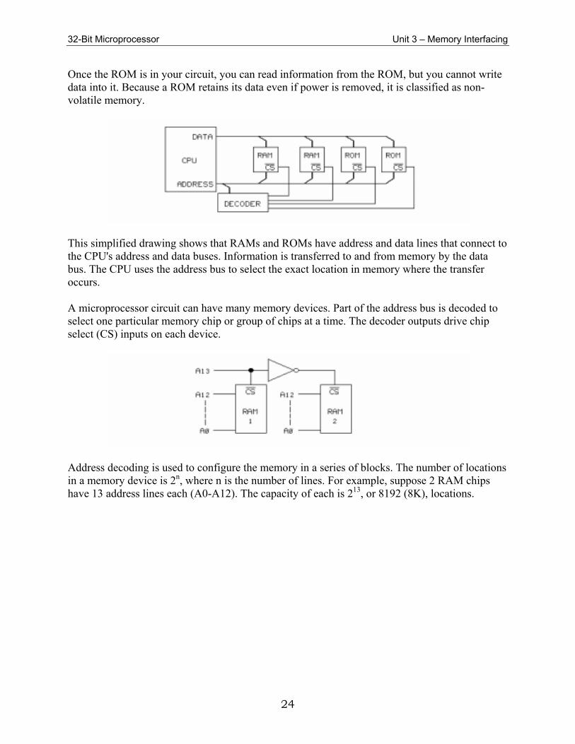
Once the ROM is in your circuit, you can read information from the ROM, but you cannot write data into it. Because a ROM retains its data even if power is removed, it is classified as non-volatile memory.
This simplified drawing shows that RAMs and ROMs have address and data lines that connect to the CPU's address and data buses. Information is transferred to and from memory by the data bus. The CPU uses the address bus to select the exact location in memory where the transfer occurs. A microprocessor circuit can have many memory devices. Part of the address bus is decoded to select one particular memory chip or group of chips at a time. The decoder outputs drive chip select (CS) inputs on each device.
Address decoding is used to configure the memory in a series of blocks. The number of locations in a memory device is 2n, where n is the number of lines. For example, suppose 2 RAM chips have 13 address lines each (A0-A12). The capacity of each is 213, or 8192 (8K), locations.

32-Bit Microprocessor Unit 3 – Memory Interfacing
25
The next higher address line (A13) can be used with a simple decoder (the inverter) to select one of two 8K RAMs.
If the next 2 address lines (A13 and A14) were decoded, you could select one of four (22) 8K RAMs.
The 80386 CPU is designed to work with both 32- and 16-bit data buses. A microprocessor system often has separate memory areas for storing data in 32- and 16-bit groups. On your circuit board, the RAM area is configured for 32-bit data. The ROM area is configured for 16-bit data.
Three of the PLDs (Programmable Logic Devices) on your circuit board are used for interfacing the CPU with memory. This simplified figure shows these PLDs and the signals associated with memory interface. PLDs allow the circuit designer to replace many other logic gates and devices with a single IC.

32-Bit Microprocessor Unit 3 – Memory Interfacing
26
U24 and U27 function as a bus controller. The bus controller is necessary to establish the proper timing and logic for efficient memory transfers. U23 functions as an address decoder. Its outputs are used to select a certain block of memory, while the lower CPU address lines specify an exact location within the selected block. The PLDs use signals from the clock circuit to ensure that their outputs are synchronous with the CPU. The bus controller uses CLK2, and CLK is common to both the bus controller and the address decoder. The memory on your circuit board consists of RAM, monitor ROM, and user ROM. Three of the address decoder outputs are used to select one of these blocks for a transfer.
RAMSEL# (RAM SELect) enables transfers to and from RAM. MROMSEL# (Monitor ROM SELect) enables transfers from the monitor ROM. UROMSEL# (User ROM SELect) enables transfers from the user ROM.
The BS16# (Bus Size 16) output signals the CPU when a transfer involves 16-bit memory devices.
The bus controller outputs are derived from the CPU status outputs and clock signals.
MWTC# (Memory WriTe Command) is active when the CPU writes to memory. MRDC# (Memory ReaD Command) is active when the CPU reads from memory.
The bus controller also generates the RDY# signal to the CPU.
32-Bit Microprocessor Unit 3 – Memory Interfacing
27
NEW TERMS AND WORDS bug - a hardware or software flaw that causes incorrect system operation. bus controller - a circuit that manages the control signals needed to transfer information between the CPU and memory or I/O. debug - to locate and correct a flaw in hardware or software. image - a memory location or block that is repeated one or more times due to partial address decoding. memory map - a listing or graphical representation describing how blocks of memory in a system are assigned. op code - the hexadecimal representation of a microprocessor instruction. operand - a number that is affected, manipulated, or operated upon. system address lines - the address lines that are common to the CPU and peripheral devices. volatile - subject to the loss of stored data when power is removed.
EQUIPMENT REQUIRED FACET base Oscilloscope, dual trace 32-BIT MICROPROCESSOR board Multimeter
NOTES ______________________________________________________________________________ ______________________________________________________________________________ ______________________________________________________________________________ ______________________________________________________________________________ ______________________________________________________________________________ ______________________________________________________________________________ ______________________________________________________________________________ ______________________________________________________________________________ ______________________________________________________________________________ ______________________________________________________________________________
32-Bit Microprocessor Unit 3 – Memory Interfacing
28
Exercise 1 – Memory Control Signals
EXERCISE OBJECTIVE When you have completed this exercise, you will be able to describe the data, address, and control signals of memory devices in a microprocessor circuit.
EXERCISE DISCUSSION
The number of address lines a device has determines the number of memory locations. The number of memory locations is; 2n, where n is the number of address lines.
The size of the memory block is determined by the number of data lines. The memory device is classified by the number of memory locations multiplied the number
of bits per location. Memory devices also have control inputs for communication with the microprocessor. Chip Select (CS) inputs allow the CPU to select this specific device. CS1# is an active low
signal. CS2 is permanently high for this trainer. The Write Enable (WE#), an active low input, specifies a read operation when high and a
write operation when low. The RAM has bidirectional data lines with tristate outputs. Tristate outputs are used to allow
several devices to share the data bus. Output Enable (OE#) is an active low input signal; when active the RAM can output its data
to the bus. When OE# is inactive, the RAM data outputs are forced to a high impedance state and are disconnected from the bus.
Four 8k X 8 Ram chips are needed to transfer 32 bits at a time. All four RAM chips on this microprocessor use the same 13 address lines (A2 through A14).
The 32-bit data bus is divided among the four RAMs, with a different 8-bit group connected to each.
When the address bus selects a RAM block location, the RAMSEL# signal from the address decoder activates all four (CS) chip selects.
When the CPU reads from RAM, MRDC# goes low at the appropriate time in the bus cycle, activating the (OE#) output enables of all four RAMs.
When the CPU writes to RAM, MWTC# goes low at the appropriate time in the bus cycle. Depending on the bytes used in the data transfer, the corresponding byte enable outputs (BE0# - BE3#) become active. The byte enables are gated with MWTC# to activate the write enable (WE#) input of the selected RAM(s).
The block diagram of the ROM is very similar to that of the RAM. The ROM data lines are labeled O0 through O7 because they are output lines only.
The ROM has one CS and one OE# control line. There is no need for a WE# line since the ROM is a read only device.

32-Bit Microprocessor Unit 3 – Memory Interfacing
29
The two monitor ROM ICs use address lines A1 through A13 and data lines D0 through D15. This makes the overall configuration of the ROMs on this circuit 8k X 16.
When the address bus specifies a memory location in the monitor ROM block, the MROMSEL# signal from the address decoder activates the ROM chip selects. MRDC# becomes active at the appropriate time in the read cycle and activates the ROM output enables. When the ROM outputs are enabled, the CPU car read data from the ROMs.
The user ROM block contains two vacant IC sockets to install ROMs which you have programmed. The address and data bus connections are identical to the monitor ROM except that the chip selects are driven by UROMSEL#.
Troubleshooting faults (bugs) in memory circuits requires a step-by-step systematic approach.
ROM memory circuits may be assumed functional if the correct start-up message appears on the LCD display.
If the start-up message does not appear begin the troubleshooting procedure by examining the address information and data used by the initialization program.
There is a RAM test program stored in the monitor ROM. This program reads and writes to RAM; by operating the CPU in the SINGLE CYCLE, mode the information can be evaluated and debugged.
Signals from the CPU are sent to several different location; for this reason, the signal should be checked at different points to confirm that it is functioning properly.
NOTES ______________________________________________________________________________ ______________________________________________________________________________ ______________________________________________________________________________ ______________________________________________________________________________ ______________________________________________________________________________ ______________________________________________________________________________ ______________________________________________________________________________ ______________________________________________________________________________ ______________________________________________________________________________ ______________________________________________________________________________
32-Bit Microprocessor Unit 3 – Memory Interfacing
30
Exercise 2 – Memory Address Decoding
EXERCISE OBJECTIVE When you have completed this exercise, you will be able to describe the memory address decoding system that is used to select individual blocks of memory.
DISCUSSION
PLD (U23) is the memory address decoder in this circuit. The PLD decodes address lines A17 and A18 and produces the memory clock select signals RAMSEL#, MROMSEL# and UROMSEL#, and signal BS16#, which is active for both MROM and UROM transfers.
The ADS# and CLK signals are used to synchronize and activate the block selects at the proper time in the bus cycle.
M/IO# is used to ensure that RAM and ROM are selected only for memory transfers, not for I/O transfers.
The RAM block is selected when bits A17 and A18 are both 0. The user ROM is selected when A17 is 0 and A18 is 1. The monitor ROM is selected when A17 and A18 are both 1. The number of byte locations in each block is determined by the lower 17 address bits (A0
through A16); producing 131,072 (128K) locations. Four bytes are required for a doubleword, therefore there are 32K doubleword locations.
Memory block allocations are designated by a memory map. Since A15 and A16 are not decoded, the 32 kilobytes section of RAM seems to be repeated
several times within the 128 kilobytes block. These duplicated sections are seen as images of the first section by the CPU and not as separate sections.
Images will contain the same data as the decoded section of memory. The number of undecoded address bits (n) determines the number of sections (2n) in a
memory block. The ROM block has three undecoded address lines (A14, A15, and A16); therefore there are
8 sections in each ROM block.

32-Bit Microprocessor Unit 3 – Memory Interfacing
31
NOTES ______________________________________________________________________________ ______________________________________________________________________________ ______________________________________________________________________________ ______________________________________________________________________________ ______________________________________________________________________________ ______________________________________________________________________________ ______________________________________________________________________________ ______________________________________________________________________________ ______________________________________________________________________________ ______________________________________________________________________________
32-Bit Microprocessor Unit 3 – Memory Interfacing
32
Exercise 3 – Memory Data Transfers
EXERCISE OBJECTIVE When you have completed this exercise, you will be able to describe 16- and 32-bit memory data transfers in an 80386 microprocessor circuit.
DISCUSSION
The CPU generates address outputs A2 through A31. A0 and A1 internally generate the four byte-enable signals (BE#0 through BE3#).
PLD (U20) decodes the byte enables to generate A0 and A1 for use by other external devices. A0 is not used for memory addressing. A1 is part of the ROM address.
A2 changes state every fourth step; since RAM is configured for doubleword (4 bytes) storage, A2 is the lowest bit needed to address RAM.
A1 changes state every second step; since ROM is configured for word (2 bytes) storage, A1 is the lowest bit needed to address ROM.
BE0# through BE3# are used to address individual bytes within a RAM doubleword. When the CPU reads ROM, both lower bytes are always transferred. The byte enables are used for RAM write cycles and not for RAM read cycles. The CPU reads all 32 data lines when it reads from RAM. The CPU will internally select
only the byte(s) required for the operation to be performed. 32-bit misaligned RAM transfers require two bus cycles. The higher doubleword location is
addressed first. The lower doubleword location is addressed in the second cycle. Misaligned transfers can occur in ROM, but the alignment is referenced to word boundaries.
Since ROM is two bytes wide, a 32-bit transfer can overlap one or two word boundaries. Two bus cycles are required if one word boundary is crossed and three bus cycles are required if two word boundaries are crossed.
Since the ROM transfers are limited to the lower 16 data lines, transfers of more than 16 bits or 16-bit misaligned words require special consideration. The CPU reads data on the lower 16 lines (D0 through D15) that it would normally read on the upper 16 lines (D16 through D31).
Normal data transfers of one or both of the lower data bytes occur on D0 through D15, when BE0# and/or BE1# are active.
Transfers involving data from D24 to D31 appear on D8 to D15, with BE1# and BE3# active. Transfers involving data from D16 to D23 appear on D0 to D7, with BE0# and BE2# active. Transfers requiring two bus cycles use the byte enable lines to determine which bytes are read in which bus cycle.
In two cycle transfers, the lower bytes are transferred first. The condition of BS16# determines the bus size. If BS16# is low during sampling, the CPU
sets the bus size to 16. If BS16# is high during sampling, the CPU sets the bus size to 32.

32-Bit Microprocessor Unit 3 – Memory Interfacing
33
NOTES ______________________________________________________________________________ ______________________________________________________________________________ ______________________________________________________________________________ ______________________________________________________________________________ ______________________________________________________________________________ ______________________________________________________________________________ ______________________________________________________________________________ ______________________________________________________________________________ ______________________________________________________________________________ ______________________________________________________________________________

32-Bit Microprocessor Unit 3 – Memory Interfacing
34
32-Bit Microprocessor Unit 4 – I/O Interfacing
35
UNIT 4 – I/O INTERFACING
UNIT OBJECTIVE At the completion of this unit, you will be able to demonstrate the signals needed to transfer data between the 386 CPU by using the 32-BIT MICROPROSSOR circuit board and its associated input/output components.
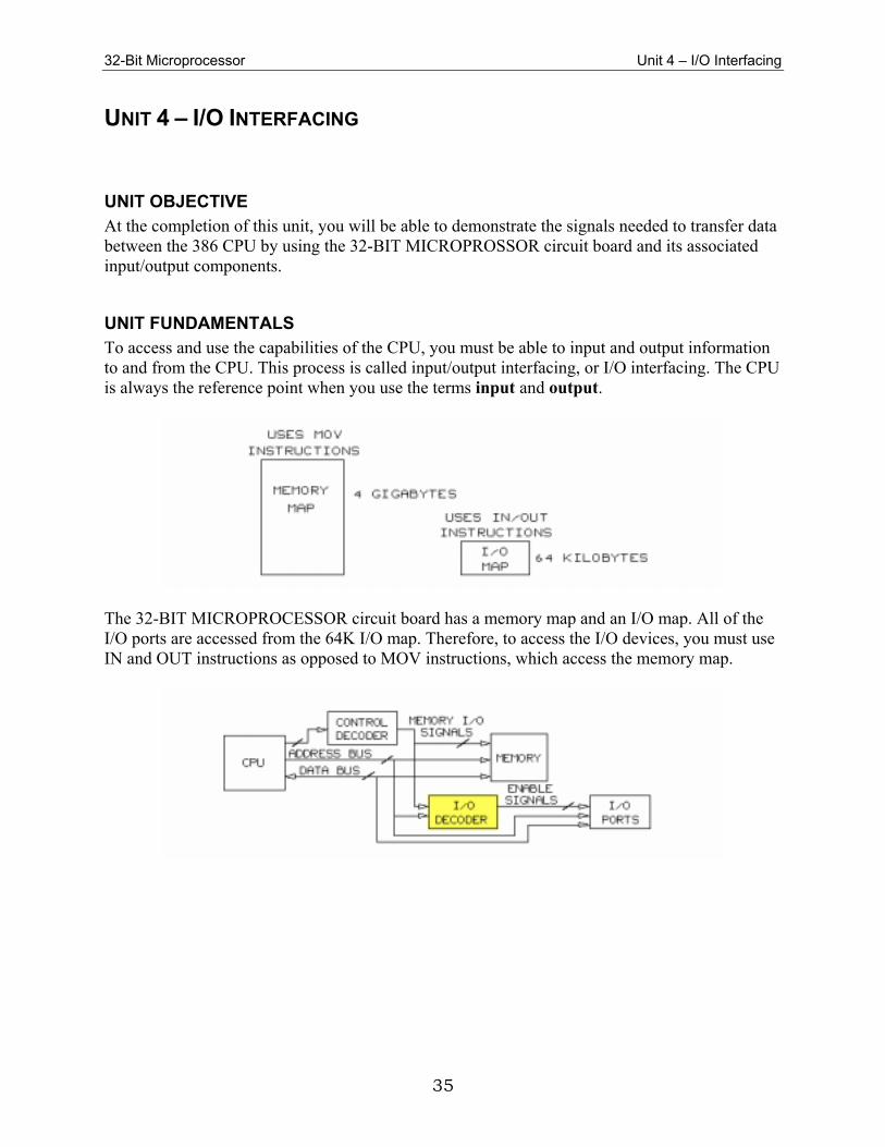
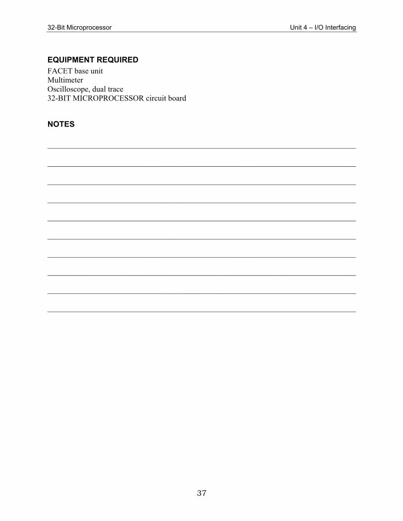
UNIT FUNDAMENTALS To access and use the capabilities of the CPU, you must be able to input and output information to and from the CPU. This process is called input/output interfacing, or I/O interfacing. The CPU is always the reference point when you use the terms input and output.
The 32-BIT MICROPROCESSOR circuit board has a memory map and an I/O map. All of the I/O ports are accessed from the 64K I/O map. Therefore, to access the I/O devices, you must use IN and OUT instructions as opposed to MOV instructions, which access the memory map.

32-Bit Microprocessor Unit 4 – I/O Interfacing
36
The I/O decoder uses address lines A4, A5, and A6 plus control signals ADS#, M/IO, IORC#, and IOWC# to enable the different I/O ports.
The 32-BIT MICROPROCESSOR circuit board has 6 input/output blocks, or I/O ports.
Each I/O port has a specific address range to access it. The display provides the user with information. The serial port is used to input and output data serially with other external devices. The peripheral interrupt controller (PIC) provides 8 interrupt inputs. Interrupts are covered in a separate unit. The DAC (digital-to-analog converter) provides an analog output. The ADC (analog-to-digital converter) provides an analog input. The programmable peripheral interface (PPI) interfaces the keypad and 8-bit parallel port to the CPU.
NEW TERMS AND WORDS bipolar - having two polarities. retriggerable one-shot - a monostable multivibrator that can be triggered during its pulse time to prevent time-out. unipolar - having one polarity.
32-Bit Microprocessor Unit 4 – I/O Interfacing
37
EQUIPMENT REQUIRED FACET base unit Multimeter Oscilloscope, dual trace 32-BIT MICROPROCESSOR circuit board
NOTES ______________________________________________________________________________ ______________________________________________________________________________ ______________________________________________________________________________ ______________________________________________________________________________ ______________________________________________________________________________ ______________________________________________________________________________ ______________________________________________________________________________ ______________________________________________________________________________ ______________________________________________________________________________ ______________________________________________________________________________
32-Bit Microprocessor Unit 4 – I/O Interfacing
38
Exercise 1 – DAC and ADC Ports
EXERCISE OBJECTIVE At the completion of this exercise, you will be able to demonstrate the DAC and ADC ports on the 32-BIT MICROPROCESSOR circuit board. You will use a program, voltmeter, and oscilloscope to verify your results.
DISCUSSION
The DAC (Digital-to-Analog Converter) takes a digital input and converts it to an analog voltage output.
The DAC on the circuit board accepts 8 binary bits as input; therefore it is referred to as an 8-bit DAC.
The number of binary inputs is an indication of the resolution of a DAC. Resolution is determined by the full-scale output voltage divided by the number of input bits.
The DAC, on the circuit board, has two ranges for output voltage, 10V and 2.56V, which can be selected by using a shunt.
The ADC (Analog-to-Digital Converter) takes an analog signal and converts it to a digital signal.
The ADC on this circuit board has an 8-bit output and two input modes of operation, unipolar and bipolar.
The unipolar mode has an input voltage range of 0V to +10V. The output is 00H with a 0V input and FFH with a 10V input.
The bipolar mode has an input voltage range -5V to +5V. The output is 00H with a -5V input, 80H with a 0V input, and FFH with a +5V.
The register in the CPU which inputs and outputs data is the AL register. The AL register is the lower 8 bits of the EAX register.

32-Bit Microprocessor Unit 4 – I/O Interfacing
39
NOTES ______________________________________________________________________________ ______________________________________________________________________________ ______________________________________________________________________________ ______________________________________________________________________________ ______________________________________________________________________________ ______________________________________________________________________________ ______________________________________________________________________________ ______________________________________________________________________________ ______________________________________________________________________________ ______________________________________________________________________________
32-Bit Microprocessor Unit 4 – I/O Interfacing
40
Exercise 2 – PPI and Keypad Interface
EXERCISE OBJECTIVE At the completion of this exercise, you will be able to demonstrate the programmable peripheral interface (PPI) and the keypad interface by using a test program and an oscilloscope.
DISCUSSION
The programmable peripheral interface (PPI) is used to interface external devices to the CPU. The PPI contains three programmable 8-bit ports. The PA ports interface the keypad and the
TEST DIP switch. The PB port connects to JP6 and is used as an 8-bit parallel port. The PC port is used for control (handshaking) signals with the PA and PB ports.
The PPI connects to data lines D0 through D7, byte 0 of the data bus. Address inputs A0 and A1 select one of the three ports. The CPU uses a control word to program the ports of the PPI. The control word defines the
operation of the three ports. To access the control word, both address lines A0 and A1 must be high.
The monitor initialization routine sets the PPI PA port as a strobed input port. When the NORM/TEST shunt is in the TEST position, the DIP switch (S3) is read on PA4 to PA7, allowing the DIP switch setting to be used to run a test routine.
When the NORM/TEST shunt is in the NORM position, the normal initialization routine is run, and the start-up message is displayed.
After initialization, the PA port is set as an input, and the key code is read on PA0 - PA3 after a key closure is sensed.
The keyscan signal (KSCLK) is a free-running clock signal, approximately 260 kHz. and is generated by the programmable logic device PLD (U20).
The KSCLK signal keeps retriggering the U40A (dual retriggerable on-shot) so the STROBE signal remains high. When a key is pressed, U40A pin 2 goes low and the KSCLK signal does not trigger the IC causing the STROBE signal to go low. The STROBE signal remains low until the key is released.
The low STROBE signal allows the PA port to latch the data on the PA lines (PA0 - PA3). When the STROBE signal goes high the CPU reads the data and processes it.

32-Bit Microprocessor Unit 4 – I/O Interfacing
41
NOTES ______________________________________________________________________________ ______________________________________________________________________________ ______________________________________________________________________________ ______________________________________________________________________________ ______________________________________________________________________________ ______________________________________________________________________________ ______________________________________________________________________________ ______________________________________________________________________________ ______________________________________________________________________________ ______________________________________________________________________________
32-Bit Microprocessor Unit 4 – I/O Interfacing
42
Exercise 3 – Display and Serial Port
EXERCISE OBJECTIVE When you have completed this exercise, you will be able to demonstrate the display and the serial poet using test routines and an oscilloscope.
DISCUSSION
The display is a 16-character by 2-line liquid crystal display (LCD). Each character is formed by a 5 by 7 dot matrix. The character generator forms the display and determines which dots are visible to form a character.
The hex code written to the display determines the character that is created by the character generator. The character generator is accessed when the register select (RS) line connected to A2 goes high at the same time DP_EN is active.
The display is connected to byte 1 of the data bus (data lines D8 through D15). A0 must be high to read or write byte 1 of the data bus.
The serial port converts a parallel byte of data to a serial data string, the LSB is transmitted first. The port converts received, serial data to parallel data. The serial port is bidirectional.
START (logic 0) and STOP (logic 1) bits are added to identify the beginning and end of a data byte. The START and STOP bits are stripped off on the receiving end before converting the data to the parallel format.
Serial data strings are used to communicate with other external serial devices. The RS232C is the serial interface communications standard. The interface uses a voltage
range of +5V to +15V for a logic 0 and -5V to -15V for a logic 1. The serial port on the 32-BIT MICROPROCESSOR circuit board conforms to this standard. An asynchronous communications interface adapter (ACIA) converts parallel data to serial
data. It inserts the START and STOP bits and transmits the serial signal at the TXD output. The ACIA receives serial data at RDX and converts it to parallel data. It performs all the functions required for serial communications. On the 32-BIT MICROPROCESSOR, IC U15 is an ACIA.
The 32-BIT MICROPROCESSOR circuit board uses voltage levels of 0 for a logic 0 and 5V for a logic 1. The RS-232C driver (U7) converts these levels to the voltage levels required by the serial port.
The RS-232C receiver (U16) converts the serial voltage levels to those required by the microprocessor board.
The header in the serial port section is used to configure the DB9 connector. This enables the port to interface with any RS-232C port.

32-Bit Microprocessor Unit 4 – I/O Interfacing
43
NOTES ______________________________________________________________________________ ______________________________________________________________________________ ______________________________________________________________________________ ______________________________________________________________________________ ______________________________________________________________________________ ______________________________________________________________________________ ______________________________________________________________________________ ______________________________________________________________________________ ______________________________________________________________________________ ______________________________________________________________________________

32-Bit Microprocessor Unit 4 – I/O Interfacing
44
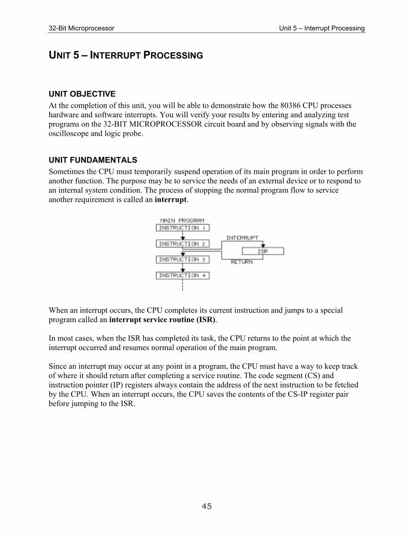
32-Bit Microprocessor Unit 5 – Interrupt Processing
45
UNIT 5 – INTERRUPT PROCESSING
UNIT OBJECTIVE At the completion of this unit, you will be able to demonstrate how the 80386 CPU processes hardware and software interrupts. You will verify your results by entering and analyzing test programs on the 32-BIT MICROPROCESSOR circuit board and by observing signals with the oscilloscope and logic probe.
UNIT FUNDAMENTALS Sometimes the CPU must temporarily suspend operation of its main program in order to perform another function. The purpose may be to service the needs of an external device or to respond to an internal system condition. The process of stopping the normal program flow to service another requirement is called an interrupt.
When an interrupt occurs, the CPU completes its current instruction and jumps to a special program called an interrupt service routine (ISR). In most cases, when the ISR has completed its task, the CPU returns to the point at which the interrupt occurred and resumes normal operation of the main program. Since an interrupt may occur at any point in a program, the CPU must have a way to keep track of where it should return after completing a service routine. The code segment (CS) and instruction pointer (IP) registers always contain the address of the next instruction to be fetched by the CPU. When an interrupt occurs, the CPU saves the contents of the CS-IP register pair before jumping to the ISR.
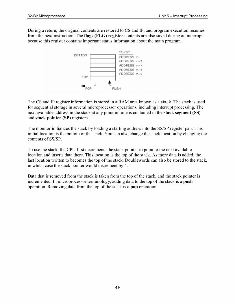
32-Bit Microprocessor Unit 5 – Interrupt Processing
46
During a return, the original contents are restored to CS and IP, and program execution resumes from the next instruction. The flags (FLG) register contents are also saved during an interrupt because this register contains important status information about the main program.
The CS and IP register information is stored in a RAM area known as a stack. The stack is used for sequential storage in several microprocessor operations, including interrupt processing. The next available address in the stack at any point in time is contained in the stack segment (SS) and stack pointer (SP) registers. The monitor initializes the stack by loading a starting address into the SS/SP register pair. This initial location is the bottom of the stack. You can also change the stack location by changing the contents of SS/SP. To use the stack, the CPU first decrements the stack pointer to point to the next available location and inserts data there. This location is the top of the stack. As more data is added, the last location written to becomes the top of the stack. Doublewords can also be stored to the stack, in which case the stack pointer would decrement by 4. Data that is removed from the stack is taken from the top of the stack, and the stack pointer is incremented. In microprocessor terminology, adding data to the top of the stack is a push operation. Removing data from the top of the stack is a pop operation.
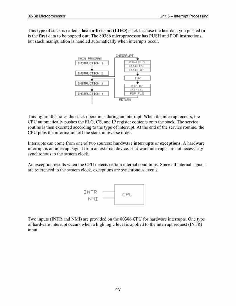
32-Bit Microprocessor Unit 5 – Interrupt Processing
47
This type of stack is called a last-in-first-out (LIFO) stack because the last data you pushed in is the first data to be popped out. The 80386 microprocessor has PUSH and POP instructions, but stack manipulation is handled automatically when interrupts occur.
This figure illustrates the stack operations during an interrupt. When the interrupt occurs, the CPU automatically pushes the FLG, CS, and IP register contents onto the stack. The service routine is then executed according to the type of interrupt. At the end of the service routine, the CPU pops the information off the stack in reverse order. Interrupts can come from one of two sources: hardware interrupts or exceptions. A hardware interrupt is an interrupt signal from an external device. Hardware interrupts are not necessarily synchronous to the system clock. An exception results when the CPU detects certain internal conditions. Since all internal signals are referenced to the system clock, exceptions are synchronous events.
Two inputs (INTR and NMI) are provided on the 80386 CPU for hardware interrupts. One type of hardware interrupt occurs when a high logic level is applied to the interrupt request (INTR) input.
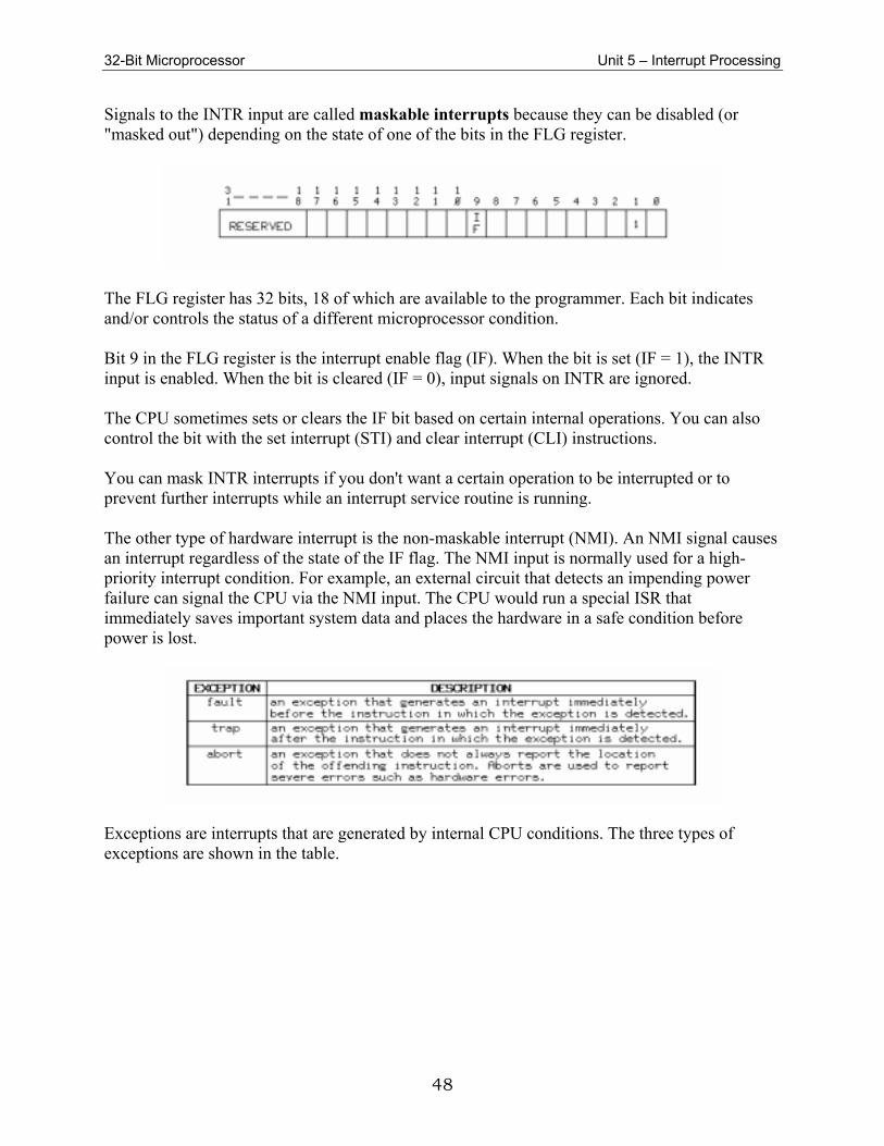
32-Bit Microprocessor Unit 5 – Interrupt Processing
48
Signals to the INTR input are called maskable interrupts because they can be disabled (or "masked out") depending on the state of one of the bits in the FLG register.
The FLG register has 32 bits, 18 of which are available to the programmer. Each bit indicates and/or controls the status of a different microprocessor condition. Bit 9 in the FLG register is the interrupt enable flag (IF). When the bit is set (IF = 1), the INTR input is enabled. When the bit is cleared (IF = 0), input signals on INTR are ignored. The CPU sometimes sets or clears the IF bit based on certain internal operations. You can also control the bit with the set interrupt (STI) and clear interrupt (CLI) instructions. You can mask INTR interrupts if you don't want a certain operation to be interrupted or to prevent further interrupts while an interrupt service routine is running. The other type of hardware interrupt is the non-maskable interrupt (NMI). An NMI signal causes an interrupt regardless of the state of the IF flag. The NMI input is normally used for a high-priority interrupt condition. For example, an external circuit that detects an impending power failure can signal the CPU via the NMI input. The CPU would run a special ISR that immediately saves important system data and places the hardware in a safe condition before power is lost.
Exceptions are interrupts that are generated by internal CPU conditions. The three types of exceptions are shown in the table.
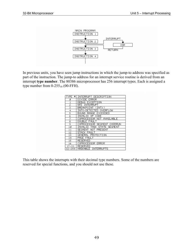
32-Bit Microprocessor Unit 5 – Interrupt Processing
49
In previous units, you have seen jump instructions in which the jump-to address was specified as part of the instruction. The jump-to address for an interrupt service routine is derived from an interrupt type number. The 80386 microprocessor has 256 interrupt types. Each is assigned a type number from 0-25510 (00-FFH).
This table shows the interrupts with their decimal type numbers. Some of the numbers are reserved for special functions, and you should not use these.
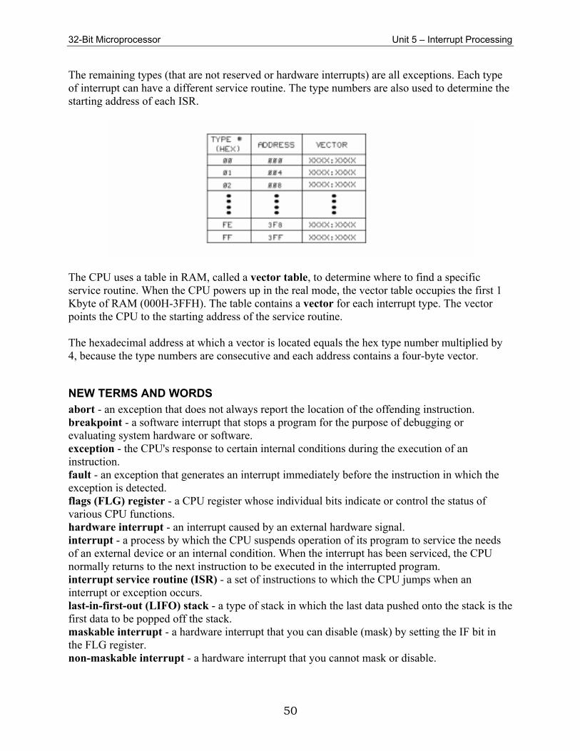
32-Bit Microprocessor Unit 5 – Interrupt Processing
50
The remaining types (that are not reserved or hardware interrupts) are all exceptions. Each type of interrupt can have a different service routine. The type numbers are also used to determine the starting address of each ISR.
The CPU uses a table in RAM, called a vector table, to determine where to find a specific service routine. When the CPU powers up in the real mode, the vector table occupies the first 1 Kbyte of RAM (000H-3FFH). The table contains a vector for each interrupt type. The vector points the CPU to the starting address of the service routine. The hexadecimal address at which a vector is located equals the hex type number multiplied by 4, because the type numbers are consecutive and each address contains a four-byte vector.
NEW TERMS AND WORDS abort - an exception that does not always report the location of the offending instruction. breakpoint - a software interrupt that stops a program for the purpose of debugging or evaluating system hardware or software. exception - the CPU's response to certain internal conditions during the execution of an instruction. fault - an exception that generates an interrupt immediately before the instruction in which the exception is detected. flags (FLG) register - a CPU register whose individual bits indicate or control the status of various CPU functions. hardware interrupt - an interrupt caused by an external hardware signal. interrupt - a process by which the CPU suspends operation of its program to service the needs of an external device or an internal condition. When the interrupt has been serviced, the CPU normally returns to the next instruction to be executed in the interrupted program. interrupt service routine (ISR) - a set of instructions to which the CPU jumps when an interrupt or exception occurs. last-in-first-out (LIFO) stack - a type of stack in which the last data pushed onto the stack is the first data to be popped off the stack. maskable interrupt - a hardware interrupt that you can disable (mask) by setting the IF bit in the FLG register. non-maskable interrupt - a hardware interrupt that you cannot mask or disable.
32-Bit Microprocessor Unit 5 – Interrupt Processing
51
overflow - a condition that occurs when the result of an arithmetic or logic operation changes the MSB (sign bit) of an operand. pop - an operation in which the CPU removes a word or doubleword from the top of the stack and then increments the stack pointer. processor-detected exception - an exception that results from the CPU's recognition of certain internal conditions. programmed exception - an exception that results from the execution of software interrupt instructions. push - an operation in which the CPU stores a word or doubleword to the top of the stack and decrements the stack pointer. sign bit - a signed operand's MSB, which indicates the algebraic sign of the operand. software interrupt - an instruction that causes a programmed exception. stack - an area of RAM set aside for sequential storage and retrieval of data. Stacks are used for several microprocessor functions, including interrupt processing. stack pointer (SP) register - a CPU register that contains the address of the last data that was pushed onto the stack. stack segment (SS) register - a CPU register that contains the segment value of the currently active stack. trap - an exception that generates an interrupt immediately after the instruction in which the exception is detected. type number - a number in the range 0-255 (00-FFH) that is used to identify the type of interrupt or exception being processed by the CPU. vector - a logical address value that points to the first location of an interrupt service routine. vector table - a table that contains the vectors for interrupt service routines. In the 80386 CPU's real mode, the vector table is normally located in the first 1 kilobyte of RAM (00-3FFH).
EQUIPMENT REQUIRED FACET base unit Oscilloscope, dual trace 32-BIT MICROPROCESSOR circuit board Multimeter

32-Bit Microprocessor Unit 5 – Interrupt Processing
52
NOTES ______________________________________________________________________________ ______________________________________________________________________________ ______________________________________________________________________________ ______________________________________________________________________________ ______________________________________________________________________________ ______________________________________________________________________________ ______________________________________________________________________________ ______________________________________________________________________________ ______________________________________________________________________________ ______________________________________________________________________________
32-Bit Microprocessor Unit 5 – Interrupt Processing
53
Exercise 1 – Non-maskable Interrupts
EXERCISE OBJECTIVE When you have completed this exercise, you will be able to demonstrate the non-maskable hardware interrupt operations of the 32-BIT MICROPROCESSOR circuit board.
DISCUSSION
The circuit shows how the non-maskable interrupt (NMI) signal is generated to the CPU on the circuit board.
The circuit's NMI output is connected directly to the CPU's active-high NMI input. The NAND gate (U38D), in the circuit, is shown as an OR gate with inverting inputs. The
output (pin 11) is high if either input (pin 12 or 13) is low. The signal from the pushbutton HALT switch (PB HALT) is latched and debounced through
inverters U29E and U29F. The resulting signal is delivered to pin 12 of U38D. Pin 13 of U38D is terminated at the NMI# pin on header JP3 (located in the CPU circuit
block). Grounding this pin generates an external non-maskable interrupt. When the NMI# input is activated, the CPU saves the CS, IP, and FLG register contents to the stack, fetches the vector for interrupt type 02, jumps to the address specified by the vector, and begins executing the service routine at that address.
The interrupt service routine (ISR) performs these functions: first saves the contents of the general purpose and segment registers, displays the address of the instruction at which the interrupt occurred, displays the contents of that address, and places the system in the function mode and waits for a keypad command.
A non-maskable interrupt is recognized at the low-to-high transition of the NMI signal and must be low for at least eight CLK2 cycles. This allows the CPU to recognize only valid NMI signals and to ignore short, transient pulses.
In the event of several successive valid NMI pulses, the CPU responds to the first pulse by executing a service routine.
If further NMI pulses occur during the ISR, the CPU saves only the first of these, executes the ISR once more upon completion of the first ISR, and ignores additional pulses.

32-Bit Microprocessor Unit 5 – Interrupt Processing
54
NOTES ______________________________________________________________________________ ______________________________________________________________________________ ______________________________________________________________________________ ______________________________________________________________________________ ______________________________________________________________________________ ______________________________________________________________________________ ______________________________________________________________________________ ______________________________________________________________________________ ______________________________________________________________________________ ______________________________________________________________________________
32-Bit Microprocessor Unit 5 – Interrupt Processing
55
Exercise 2 – Maskable Interrupts
EXERCISE OBJECTIVE At the completion of this exercise, you will be able to explain and demonstrate the operation of maskable hardware interrupts for the 80386 microprocessor.
DISCUSSION
Maskable interrupts occur when the CPU's INTR (interrupt request) input is activated, or driven high.
A special support chip called a programmable interrupt controller (PIC) interfaces external maskable interrupt signals to the CPU.
The PIC has eight data I/O lines, which connect to the lower eight bits (D0-D7) of the system data bus. This connection allows the CPU to send programming information to the PIC and allows the PIC to send an interrupt type number to the CPU.
The read (RD) and write (WR) inputs are driven by the I/O read command (IORC#) and I/O write command (IOWC#) signals, respectively. These signals are generated by the bus control PLD and are necessary for communication between the PIC and the CPU.
The PIC is addressed by the PIC_EN# signal from the I/O decoder PLD. PIC_EN# drives the PIC's chip select (CS) input.
The A0 address input to the PIC is driven by A2 from the system address bus. The PIC uses this input to decipher command words sent from the CPU and status words sent to the CPU.
There are eight interrupt request inputs (IR0-IR7) on the PIC for interrupt signals from external devices. When one or more of the IR inputs are activated, the PIC generates an interrupt request to the CPU.
When the CPU finishes executing its current instruction, the PIC receives an interrupt acknowledge (INTA#) signal from the bus controller PLD.
The eight IR inputs are wired to header JP4 allowing them to be connected to other circuit blocks or to external devices, easily.
The interrupt request lines are connected only to pull-down resistors and to one row of pins on header JP4. This is the bottom row of pins. Any of the IR lines can be activated by connecting +5V to its pin. Shunts can be used to interconnect the interrupt request lines, IR1-IR5, to other circuit blocks.
The pin adjacent to IR1 is labeled COM (communications) and is used as an interrupt request from the SERIAL PORT circuit block.
IR2 and IR3 are general-purpose interrupt requests (INTRA and INTRB) that the CPU can output via the PPI.
IR4 can be connected to the RXC output from the SERIAL PORT block. RXC is a clock signal derived from the ACIA's crystal oscillator. Use IR4 as a clock source in programs when timing applications are required.
32-Bit Microprocessor Unit 5 – Interrupt Processing
56
IR5 can be connected to the data ready (DR#) output from the analog-to-digital converter (ADC) circuit block.
Placing a shunt in the IR5/DR# position allows the CPU to be interrupted when the ADC completes its conversion.
Before normal processing of maskable interrupts can begin, the CPU must output from two to four initialization command words (ICW) to the PIC. The flow diagram shows the sequence for initializing the PIC.
There are four ICWs (ICW1 through ICW4). Programming always begins with ICW1, followed by ICW2. The eight data bits of the ICW, in conjunction with the state of the A0 input, set the initial configuration of the PIC. ICW1 is characterized by the conditions A0 = 0 and D4 = 1.
Each data bit controls a function or condition in the PIC. Setting D1 to 1 specifies that a single (SNGL) PIC is used in the system. D1 is set to 0 to specify cascade mode (more than one PIC used). If command word ICW4 is also needed to program the PIC, then bit D0 in ICW1 is set to 1. D0 = 0 if ICW4 is not needed.
Some data bits in the command words have fixed values. Some of these bits are not used, and some are reserved for use with different microprocessors or system configurations.
ICW2 contains the type numbers of the eight interrupt requests (IR0-IR7) of the PIC being programmed. The programmer specifies the upper five data bits (D3-D7).
If ICW4 is needed, the only bit you may need to change in this system is D1, which controls the end of interrupt (EOI) mode.
When D1 = 0, the normal EOI mode is selected. In this mode, an interrupt sequence ends when the CPU issues an EOI command to the PIC.
When D1 = 1, the mode selected is automatic end of interrupt (AEOI). In the AEOI mode, an interrupt sequence ends automatically when a second interrupt acknowledge pulse is received from the CPU.
Once the ICWs have initialized the PIC, the CPU can issue commands to the PIC by outputting operation command words (OCW).
The OCWs can mask (disable) one or more of the IR inputs, set the priorities of the IR inputs so that more important system functions are first to be
serviced, allow the CPU to read status information from the PIC, and set up special operating modes.
The CPU has a special timing sequence for handling maskable interrupts. The sequence consists of two interrupt acknowledge (INTA) cycles separated by four idle states.
When an interrupt request is received, the CPU responds by issuing the first INTA cycle. The outputs BE0#, A3 - A31, M/IO#, D/C#, and W/R# are all driven low.
The control signal levels define a unique bus cycle type. Also during the first INTA cycle, the CPU drives A2 and the remaining byte enables high.
The first INTA cycle is followed by four consecutive idle states. The idle states are followed by the second INTA cycle. At the end of the second INTA cycle,
the CPU reads the eight-bit vector type number from the PIC on data lines D0-D7.

32-Bit Microprocessor Unit 5 – Interrupt Processing
57
NOTES ______________________________________________________________________________ ______________________________________________________________________________ ______________________________________________________________________________ ______________________________________________________________________________ ______________________________________________________________________________ ______________________________________________________________________________ ______________________________________________________________________________ ______________________________________________________________________________ ______________________________________________________________________________ ______________________________________________________________________________
32-Bit Microprocessor Unit 5 – Interrupt Processing
58
Exercise 3 – Exceptions
EXERCISE OBJECTIVE At the completion of this exercise, you will be able to explain and demonstrate how exceptions interrupt the 80386 microprocessor.
DISCUSSION
There are two ways exceptions can interrupt the microprocessor. Exceptions can be programmed using the INT3, INTO, or INTn instructions in a program. Some of these instructions are called software interrupts and require specific conditions to exist in order to generate an interrupt.
Processor-detected exceptions do not depend on a program instruction, they occur automatically if specific conditions arise within the CPU.
The interrupt type number determines the vector that points to the correct service routine. The number is required for either type of exception and is assigned by the CPU.
The INT3 software interrupt (or breakpoint) has a type number of 3. The ISR’s vector is located at 0000CH. INT3 can be inserted into a program in place of any instruction. The CPU will stop executing program commands when it reaches the INT3 instruction allowing the examination of registers, memory, or hardware conditions.
The INTO (interrupt on overflow) is a conditional software interrupt causing a type 4 interrupt only when an overflow condition exists. The CPU sets the overflow (OF) flag, which is bit 11 in the flags register. Once the interrupt is cleared the next instruction is executed.
INTn is a software interrupt that is useful in debugging programs or aiding system development. The op code for INTn is CD n, where n is a one-byte type number from 00H-FFH. These values are tabulate in the text.
A programmer must verify that a vector table is established with the appropriate service routine for each exception.
On this circuit board many of the service routines write a message to the display to inform you that the exception was detected.

32-Bit Microprocessor Unit 5 – Interrupt Processing
59
NOTES ______________________________________________________________________________ ______________________________________________________________________________ ______________________________________________________________________________ ______________________________________________________________________________ ______________________________________________________________________________ ______________________________________________________________________________ ______________________________________________________________________________ ______________________________________________________________________________ ______________________________________________________________________________ ______________________________________________________________________________

32-Bit Microprocessor Unit 5 – Interrupt Processing
60
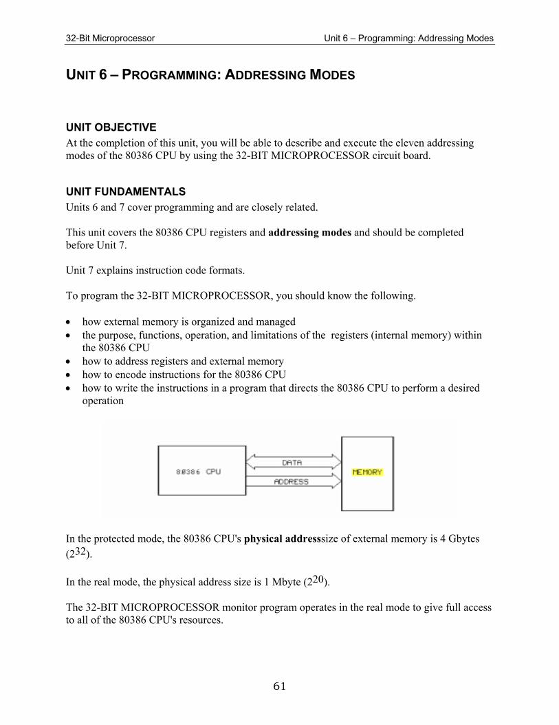
32-Bit Microprocessor Unit 6 – Programming: Addressing Modes
61
UNIT 6 – PROGRAMMING: ADDRESSING MODES
UNIT OBJECTIVE At the completion of this unit, you will be able to describe and execute the eleven addressing modes of the 80386 CPU by using the 32-BIT MICROPROCESSOR circuit board.
UNIT FUNDAMENTALS Units 6 and 7 cover programming and are closely related. This unit covers the 80386 CPU registers and addressing modes and should be completed before Unit 7. Unit 7 explains instruction code formats. To program the 32-BIT MICROPROCESSOR, you should know the following. how external memory is organized and managed the purpose, functions, operation, and limitations of the registers (internal memory) within
the 80386 CPU how to address registers and external memory how to encode instructions for the 80386 CPU how to write the instructions in a program that directs the 80386 CPU to perform a desired
operation
In the protected mode, the 80386 CPU's physical addresssize of external memory is 4 Gbytes
(232).
In the real mode, the physical address size is 1 Mbyte (220). The 32-BIT MICROPROCESSOR monitor program operates in the real mode to give full access to all of the 80386 CPU's resources.

32-Bit Microprocessor Unit 6 – Programming: Addressing Modes
62
The 32-BIT MICROPROCESSOR circuit board's physical memory map is shown. The circut board contains 32 Kbytes of RAM from address 00000 to 07FFF. User ROM exists at address 40000 to 4FFFF. Monitor ROM exists at address 60000 to 6FFFF. Address 20000 to 2FFFF is open. The remaining memory addresses are image addresses. For example, address 08000 is an image address of 00000; both addresses have the same physical location on the 32-BIT MICROPROCESSOR circuit board. Memory management for the 80386 CPU consists of paging and segmentation. Paging, which may be used only in the protected mode, provides access to data structures and programs larger than the available memory space.
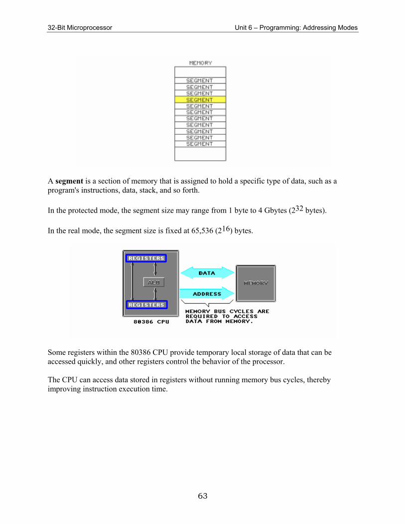
32-Bit Microprocessor Unit 6 – Programming: Addressing Modes
63
A segment is a section of memory that is assigned to hold a specific type of data, such as a program's instructions, data, stack, and so forth.
In the protected mode, the segment size may range from 1 byte to 4 Gbytes (232 bytes).
In the real mode, the segment size is fixed at 65,536 (216) bytes.
Some registers within the 80386 CPU provide temporary local storage of data that can be accessed quickly, and other registers control the behavior of the processor. The CPU can access data stored in registers without running memory bus cycles, thereby improving instruction execution time.
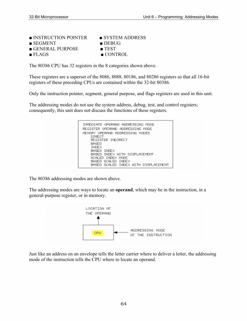
32-Bit Microprocessor Unit 6 – Programming: Addressing Modes
64
■ INSTRUCTION POINTER ■ SYSTEM ADDRESS ■ SEGMENT ■ DEBUG ■ GENERAL PURPOSE ■ TEST ■ FLAGS ■ CONTROL The 80386 CPU has 32 registers in the 8 categories shown above. These registers are a superset of the 8086, 8088, 80186, and 80286 registers so that all 16-bit registers of these preceding CPUs are contained within the 32-bit 80386. Only the instruction pointer, segment, general purpose, and flags registers are used in this unit. The addressing modes do not use the system address, debug, test, and control registers; consequently, this unit does not discuss the functions of these registers.
The 80386 addressing modes are shown above. The addressing modes are ways to locate an operand, which may be in the instruction, in a general-purpose register, or in memory.
Just like an address on an envelope tells the letter carrier where to deliver a letter, the addressing mode of the instruction tells the CPU where to locate an operand.
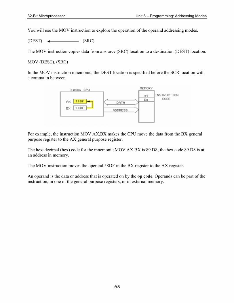
32-Bit Microprocessor Unit 6 – Programming: Addressing Modes
65
You will use the MOV instruction to explore the operation of the operand addressing modes. (DEST) (SRC) The MOV instruction copies data from a source (SRC) location to a destination (DEST) location. MOV (DEST), (SRC) In the MOV instruction mnemonic, the DEST location is specified before the SCR location with a comma in between.
For example, the instruction MOV AX,BX makes the CPU move the data from the BX general purpose register to the AX general purpose register. The hexadecimal (hex) code for the mnemonic MOV AX,BX is 89 D8; the hex code 89 D8 is at an address in memory. The MOV instruction moves the operand 58DF in the BX register to the AX register. An operand is the data or address that is operated on by the op code. Operands can be part of the instruction, in one of the general purpose registers, or in external memory.
32-Bit Microprocessor Unit 6 – Programming: Addressing Modes
66
NEW TERMS AND WORDS addressing modes - ways to write instruction, codes to locate an operand which may be in the instruction in a general-purpose register or in memory. physical address - an address that uniquely identifies a location in memory. image addresses - different addresses that refer to the same memory location due to partial address decoding. paging - a memory management method that is used in the protected mode to provide access to data structures and programs larger than the available memory space. segmentation - a memory management method that allows memory to be divided into independent secure address spaces. segment - an independent secure address space. operand - the data or address that is operated on by the op code. op code - the part of the instruction that contains the code for the microprocessor operation to be performed on the operand. base address - the first location in a segment. segment selector values - the 16-bit values that are in the visible part of the segment register. hidden descriptor - the hidden part of a segment register that contains the segment's base address, limit, and access information limit - defines the size of a segment. access information - information contained in the segment register's hidden descriptor; it controls what programs can access data in a segment. descriptor table - a table in memory that contains information for the hidden part of a segment register. linear address - an address equal to the segment's base address plus the offset, which determines the physical address when paging is activated. logical address - a representation of the physical address, written in the form of segment selector value: offset value; The segment selector value is 2 bytes, and the offset value may be 2 or 4 bytes. effective address (EA) - an offset (calculated from the sum of displacement, base, and index values) that locates a memory operand within a selected segment.
EQUIPMENT REQUIRED FACET base unit 32-BIT MICROPROCESSOR circuit board Multimeter Oscilloscope, dual trace

32-Bit Microprocessor Unit 6 – Programming: Addressing Modes
67
NOTES ______________________________________________________________________________ ______________________________________________________________________________ ______________________________________________________________________________ ______________________________________________________________________________ ______________________________________________________________________________ ______________________________________________________________________________ ______________________________________________________________________________ ______________________________________________________________________________ ______________________________________________________________________________ ______________________________________________________________________________
32-Bit Microprocessor Unit 6 – Programming: Addressing Modes
68
Exercise 1 – Immediate and Register Addressing Modes
EXERCISE OBJECTIVE When you have completed this exercise, you will be able to explain the functions of the registers within the 80386 CPU use the immediate and register addressing modes to transfer an operand to a register. You will verify your results by reading the contents of the register before and after execution
of a move (MOV) instruction.
DISCUSSION
There are four types of registers within the 80386 CPU, they are the instruction pointer, segment, general purpose, and flags registers.
The flags register is a 32-bit register named EFLAGS. The contents control certain operations and indicate the status of the 80386 CPU. The full 32-bit register is only used in the protected mode. The FLAGS register, the first 16 bits of EFLAGS, is used in the real and protected modes.
The instruction pointer register is a 32-bit register named EIP. The content is the offset value for the address of the next instruction in memory. The offset value is always added to the base address in the code segment (CS) register, the sum provides the physical address of the next instruction. The first 16 bits contain the 16-bit instruction pointer named IP. Since the 80386 operates in the real mode, the 16-bit IP is used in these exercises.
There are six segment registers which hold information for the currently addressable memory segments. The six active segments are the ones whose 16-bit segment selector values occupy the segment registers. The program changes the selector value in a segment register to access a new segment in RAM when there are more that six segments.
Every segment has two parts, a 16-bit visible part containing the segment selector value, and a hidden descriptor part that the processor automatically loads with the segment’s 32-bit base address, limit, and access information.
The selector value is used, in the protected mode, to pick one of 8192 (213) possible descriptors from a descriptor table in memory. The descriptor table provides the information for the hidden descriptor part of the segment register.
In the protected mode, the CPU adds the offset to the 32-bit base address to form a linear address. If paging is inactive, the linear address is the physical address in memory. If paging is active, data structures and programs may be partly in memory and partly in disk storage.
Paging provides access to data structures and programs that are larger than the available memory space.
32-Bit Microprocessor Unit 6 – Programming: Addressing Modes
69
In the real mode, segment descriptor tables are not used. The CPU contains the base address by shifting the 16-bit segment selector value 4 bits to the left. Only the lower 20 bits of the 32-bit base address in the segment register’s hidden descriptor are significant. When a new selection value is entered only the base address in the segment register’s hidden part is updated.
There are eight 32-bit general purpose registers. They are EAX, EDX, ECX, EBX, ESP, EBP, ESI, and EDI. All of these registers are available for address calculations when the CPU uses 32-bit addressing.
The lower 16 bits of the general purpose registers are referenced using their 8086 names; AX, DX, CX, BX, BP, SI, DI, and SP. Each byte of the 16-bit registers AX, DX, CX, and BX have names. The high bytes are AH, DH, CH, and BH while the lower bytes are AL, DL, CL, and BL.
In the real mode, instructions that use a 32-bit general-purpose register require the 32-bit operand prefix. When the operand is data, the prefix is a byte with a hex value of 66 placed before the rest of the instruction.
Instructions that specify a general purpose register as a destination can change the low order bytes on all of the bytes in the register. When the operand contains fewer bytes than the register, the high order bytes of the register are left unchanged.
The addressing modes are ways to locate an operand, which may be in the instruction, in a general register, or in memory. In the immediate operand addressing mode, the operand is included as part of the instruction code. In the register operand addressing mode, the operand is in a general purpose register.
NOTES ______________________________________________________________________________ ______________________________________________________________________________ ______________________________________________________________________________ ______________________________________________________________________________ ______________________________________________________________________________ ______________________________________________________________________________ ______________________________________________________________________________ ______________________________________________________________________________ ______________________________________________________________________________ ______________________________________________________________________________
32-Bit Microprocessor Unit 6 – Programming: Addressing Modes
70
Exercise 2 – Memory Addressing Modes - I
EXERCISE OBJECTIVE When you complete this exercise, you will be able to describe the ways to determine the effective address of a memory operand by using
displacement, base and index values explain the six memory operand addressing modes that can be used for 16-bit and 32-bit
addressing. You will verify your results by reading the contents of a register before and after execution of
a move (MOV) instruction.
DISCUSSION
The memory operand addressing mode locates an operand in memory. The instruction code must reference the offset and segment of the address containing the
memory operand in order for it to be found. The 80386 CPU determines the physical address of a memory operand by calculating an
effective address (EA), The effective address is the sum of the offset and the segment’s base address.
The 80386 CPU calculates the EA from one of six combinations of a displacement value, base value, or an index value for 16-bit and 32-bit addressing.
In 32-bit addressing the index value may be multiplied by a scale factor of 1, 2, 4, or 8. The use of a scale factor provides 3 additional combinations of displacement, base, and index values for calculating the effective address.
The displacement value appears in the displacement field of the instruction code. With 16-bit addressing, the BX or BP general-purpose registers can contain the base value.
The SI or DI registers can contain the index value. Any of the eight general purpose registers can contain the base value or the index value
(except ESP) for 32-bit addressing. An index value scale factor can be used in 32-bit addressing only. The six memory addressing modes, for 16-bit and 32-bit addressing, are: direct, register
indirect, based, index, based index, and based index with displacement. In 32-bit addressing, an index value scale factor permits three additional addressing modes;
they are scaled index, based scaled index, and based scaled index with displacement. Instructions do not need to explicitly specify the segment register to provide compact
instruction encoding and increase processor performance.

32-Bit Microprocessor Unit 6 – Programming: Addressing Modes
71
When the base value is in the EAX, EBX, ECX, EDX, ESI, or EDI registers, the DS segment is used for the memory operand by default. The CPU calculates the physical address of the data by adding the effective address to the DS segment base address.
When the base value is in the EBP or ESP registers, the default segment is the SS segment. The CPU calculates the physical address of the data by adding the effective address to the SS segment’s base address.
In general, instruction code fetches use the CS register; the CS register contains the base address for the code segment of the instruction code. When the CPU fetches the next instruction code, it determines the instruction’s physical address by adding the offset in the IP register to the code segment base address.
When the CPU fetches the next stack code, it determines the stack’s physical address by adding the offset in the SP register to the stack segment’s base address.
Instruction codes must have prefixes for 32-bit addressing and 32-bit operands. 32-bit addresses require the address size hexadecimal 67. 32-bit operands require the operand size hexadecimal prefix 66. If both are required the address prefix (67) comes before the operand (66).
NOTES ______________________________________________________________________________ ______________________________________________________________________________ ______________________________________________________________________________ ______________________________________________________________________________ ______________________________________________________________________________ ______________________________________________________________________________ ______________________________________________________________________________ ______________________________________________________________________________ ______________________________________________________________________________ ______________________________________________________________________________
32-Bit Microprocessor Unit 6 – Programming: Addressing Modes
72
Exercise 3 – Memory Addressing Modes - II
EXERCISE OBJECTIVE When you complete this exercise, you will be able to determine the effective address of a memory operand by using displacement, base, and scaled
index values, explain the three 32-bit memory operand addressing modes that use a scaled index. You will verify your results by reading the contents of a register before and after execution of
a move (MOV) instruction.
DISCUSSION
The index value may be multiplied by a scale factor of 1, 2, 4, or 8 when in 32-bit addressing mode. This multiplication gives three additional combinations of displacement, base, and index values which can be used to calculate the effective address.
In real mode, the 32-bit address size hexadecimal prefix (67) must be used before any instruction code for the three addressing modes.
The three 32-bit memory addressing modes that use a scaled index value are: scaled index mode, based scaled index, and base scaled index with displacement.
Calculating the effective address using a scaled index is an efficient way to point into a list of operands when the element size is 2, 4, or 8 bytes.

32-Bit Microprocessor Unit 6 – Programming: Addressing Modes
73
NOTES ______________________________________________________________________________ ______________________________________________________________________________ ______________________________________________________________________________ ______________________________________________________________________________ ______________________________________________________________________________ ______________________________________________________________________________ ______________________________________________________________________________ ______________________________________________________________________________ ______________________________________________________________________________ ______________________________________________________________________________

32-Bit Microprocessor Unit 6 – Programming: Addressing Modes
74
32-Bit Microprocessor Unit 7 – Programming: 80386 Instructions
75
UNIT 7 – PROGRAMMING: 80386 INSTRUCTIONS
UNIT OBJECTIVE At the completion of this unit, you will be able to write instructions for the 80386 CPU with machine codes and use the instructions in memory test programs that you will run by using the 32-BIT MICROPROCESSOR circuit board.
UNIT FUNDAMENTALS Unit 6 and 7 cover programming and are closely related. This unit explains instruction code formats and programming. Unit 6 is about the 80386 CPU registers and addressing modes and should be completed before this unit. The 80386 CPU has over 100 basic instructions; some examples are shown in the help window (click on <Help>). From these basic instructions you can create well over 1000 variations. In Unit 6 you used many variations of the MOV (move) instruction. When addressing modes and data types (byte, word, or doubleword) are considered, there are over 50 possible forms of the MOV instruction. This unit will not cover the full instruction set of the 80386 CPU. Exercise 1 and 2 cover encoding multibyte MOV instructions into machine language. MEMORY TEST PROGRAM Exercise 3 and 4 describe how the MOV (move), INC (increment), CMP (compare), JMP (jump), and INT (interrupt) instructions can be combined to form a simple loop program and a memory test program, which is shown in the help window (click on <Help>). For a detailed explanation of the 80386 CPU instruction codes and programming, refer to the 386TM DX Microprocessor Programmer's Reference Manual, 1990, published by the Intel Corporation, Literature Sales, Mt. Prospect, IL 60056.
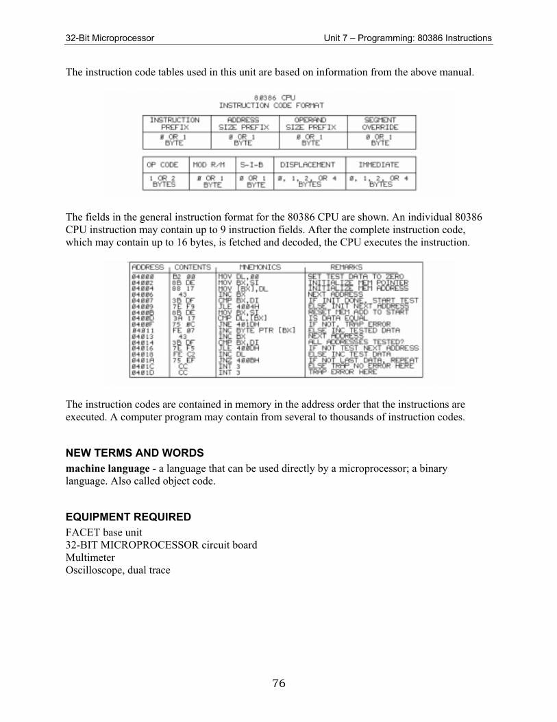
32-Bit Microprocessor Unit 7 – Programming: 80386 Instructions
76
The instruction code tables used in this unit are based on information from the above manual.
The fields in the general instruction format for the 80386 CPU are shown. An individual 80386 CPU instruction may contain up to 9 instruction fields. After the complete instruction code, which may contain up to 16 bytes, is fetched and decoded, the CPU executes the instruction.
The instruction codes are contained in memory in the address order that the instructions are executed. A computer program may contain from several to thousands of instruction codes.
NEW TERMS AND WORDS machine language - a language that can be used directly by a microprocessor; a binary language. Also called object code.
EQUIPMENT REQUIRED FACET base unit 32-BIT MICROPROCESSOR circuit board Multimeter Oscilloscope, dual trace
32-Bit Microprocessor Unit 7 – Programming: 80386 Instructions
77
NOTES ______________________________________________________________________________ ______________________________________________________________________________ ______________________________________________________________________________ ______________________________________________________________________________ ______________________________________________________________________________ ______________________________________________________________________________ ______________________________________________________________________________ ______________________________________________________________________________ ______________________________________________________________________________ ______________________________________________________________________________
32-Bit Microprocessor Unit 7 – Programming: 80386 Instructions
78
Exercise 1 – Instruction Formats - I
EXERCISE OBJECTIVE When you have competed this exercise, you will be able to encode, into machine language, multibye move (MOV) instructions for the immediate addressing mode and register addressing modes. You will verify your results by executing the instructions that you encode and by reading the contents of registers and memory locations.
EXERCISE DISCUSSION
The MOV (move) instruction may contain these main fields: address size prefix operand size prefix segment override op code mod r/m (mode register/memory) s-i-b (scale-index-base) immediate fields
In the real mode, instructions involving 32-bit addresses require a hex 67 prefix, and instructions involving 32-bit operands require a hex 66 prefix.
Tables of segment register selection rules and alternate segment hexadecimal prefixes are provided.
The first byte of the MOV instruction contains the op code, the direction (d), and the operand size (w) fields. Bits 7 to 2 contain the op code. The d bit designates if the register (specified in the register section of the mod r/m field) is the operand’s source (d=0) or destination (d=1) location.
The operand size (w field) is set to 8 bits when w=0 and 16 or 32 bits when w=1. The mod r/m byte contains three fields: mod (mode), reg (register), and r/m
(register/memory). The mod (mode) field requires 2 bits of information and determines if the operand is moved
from or to memory (00,01,10) or moved from a register to a register (11). Three bits are required in the reg field and designate which general purpose register will be
used. Tabulate data used to specify the required register is provided. An immediate operand MOV instruction includes the reg field and the w field in the first byte
of the instruction. The r/m field is a three bit code. The w bit combined with the value of the r/m field
determines the second general register to be used. Tabulated data is provided. The third, and last, byte that comprises a complete MOV instruction is the s-i-b byte.

32-Bit Microprocessor Unit 7 – Programming: 80386 Instructions
79
NOTES ______________________________________________________________________________ ______________________________________________________________________________ ______________________________________________________________________________ ______________________________________________________________________________ ______________________________________________________________________________ ______________________________________________________________________________ ______________________________________________________________________________ ______________________________________________________________________________ ______________________________________________________________________________ ______________________________________________________________________________

32-Bit Microprocessor Unit 7 – Programming: 80386 Instructions
80
Exercise 2 – Instruction Formats - II
EXERCISE OBJECTIVE When you have completed this exercise, you will be able to Encode, into machine language, multibye instructions used for the move (MOV) instruction
with the memory addressing modes, Understand how to format other 80386 CPU instruction codes. You will verify your results by executing the instructions that you encode and by reading the contents of registers and memory locations.
EXERCISE DISCUSSION
Memory addressing mode applications of the MOV instruction are discussed in this exercise. In memory addressing mode, the r/m field specifies how the 80386 CPU calculates the
effective address (EA). When the effective address calculation contains a scaled index value, the instruction code
must have an s-i-b byte. Three fields compose the s-i-b byte: ss, index, and base. The ss field specifies a scale factor of 1, 2, 4, or 8. The index field specifies the index register. The base field specifies the base register.

32-Bit Microprocessor Unit 7 – Programming: 80386 Instructions
81
NOTES ______________________________________________________________________________ ______________________________________________________________________________ ______________________________________________________________________________ ______________________________________________________________________________ ______________________________________________________________________________ ______________________________________________________________________________ ______________________________________________________________________________ ______________________________________________________________________________ ______________________________________________________________________________ ______________________________________________________________________________

32-Bit Microprocessor Unit 7 – Programming: 80386 Instructions
82
Exercise 3 – Using the 80386 CPU Instructions - I
EXERCISE OBJECTIVE When you have completed this exercise, you will be able to create a simple loop program to test a memory address by using 80386 CPU instructions. You will verify your results by observing the display and/or address and data LEDs.
EXERCISE DISCUSSION
In this exercise, you will enter a program into RAM which will illustrate how four instructions are combined to form a simple loop test program.
The program uses two MOV instructions to access memory twice by writing and reading the test data between the AX register and effective address 6050.
By using the unconditional jump instruction (JMP) with the MOV instructions, a simple test loop program is created.
In the unconditional jump instruction mnemonic JMP 2003H, the 2003H is the value of the instruction pointer after execution of the jump instruction.
The jump instruction causes the program to continuously execute the instructions between addresses 02003 to 02009.
For a short jump (fewer than +127 or -128 bytes), the first byte EB in the JMP instruction code is the JMP instruction op code.
The second byte (F8) is the positive or negative change of the instruction pointer value that the JMP instruction will cause.
Because the IP's value must decrease in this jump, F8 is the negative change of the instruction pointer.
After executing the two byte jump instruction at address 02009, the instruction pointer returns from 0200B to 02003.
The jump instruction causes the IP to return from 0200B to 02003, which is a negative 8 bytes.
For the JMP instruction to subtract 8 bytes from the IP, the 2's complement of hex 08, which is hex F8, must be used in the instruction code.

32-Bit Microprocessor Unit 7 – Programming: 80386 Instructions
83
NOTES ______________________________________________________________________________ ______________________________________________________________________________ ______________________________________________________________________________ ______________________________________________________________________________ ______________________________________________________________________________ ______________________________________________________________________________ ______________________________________________________________________________ ______________________________________________________________________________ ______________________________________________________________________________ ______________________________________________________________________________
32-Bit Microprocessor Unit 7 – Programming: 80386 Instructions
84
Exercise 4 – Using the 80386 CPU Instructions - II
EXERCISE OBJECTIVE When you have completed this unit, you will be able to use 80386 CPU instructions to create a program that tests a range of memory addresses. You will verify your results by observing the display and/or address and data LEDs
EXERCISE DISCUSSION
The program is essentially the same as the memory test program the 32-BIT MICROPROCESSOR circuit board performs if the NORM/TEST shunt in the PARALLEL PORT circuit block is in the TEST position and the DIP SWITCH is set for PA7-PA4 equals 1111.
When the defective address is found, the RAM chip associated with the address can be easily located.
In the program, register SI contains the offset value for the starting address for the memory section to be tested, and register DI contains the offset value for the ending address.
The DS register selector value will be set to 0000 (base address equal to 0000). Register BX contains the offset value to the DS's base address for the current test address. Register DL contains the data that is used to test each memory address (location). The test
data is incremented by 1 each time through the loops from byte 00 to byte FF. The first 6 six instructions (04000 to 04009) initialize each address to be tested with the test
data 00; the program keeps looping between 04004 and 04009 until all memory addresses contain hex 00.
The next instruction (0400B) resets the memory address to the starting address, whose offset value is contained in the SI register.
The following 2 instructions (0400D and 0400F) test a specific memory address for the test data.
If the data in the memory address and the DL register are the same, the test data in the address that was tested is incremented by the instruction at 04011.
The next 3 instructions (04013 to 04016) increment the address offset value in the BX register by hex 01 and compare the offset value in BX to the ending offset value in DI. If the BX offset value is less than or equal to the DI offset value, the program jumps back to address 0400D to test the next memory location.
The program keeps looping between 0400D and 04016 until all memory addresses are tested. If the BX offset value is greater than the DI offset value, the instruction at 04018 increments
the test data in the DL register by 1.
32-Bit Microprocessor Unit 7 – Programming: 80386 Instructions
85
The next instruction, JNZ 400BH, checks the value of the test data. If the test data in register DL is not 00, which would occur when hex 01 is added to FF, the
program jumps back to address 0400B to test all memory addresses with the incremented test data.
The last two instructions (0401C and 0401D) are interrupts. If there are no errors, the memory test program ends after the interrupt at 0401C. If the instructions CMP DL,[BX] and JNE 401DH at the respective addresses 0400D and
0400F detect an error (the data in the address and the BX register are not equal), the program jumps to the interrupt at 0401D and stops.
If an error is detected, the BX register contains the offset value of the address containing the fault.
There are 3 loops in the program; the first loop, 04004 to 04009, initializes the addresses to be tested with hex 00.
The address 0400B to 0401A loop occurs after each address is tested with the same data. The BX register is reset with the starting address and each address is tested again.
NOTES ______________________________________________________________________________ ______________________________________________________________________________ ______________________________________________________________________________ ______________________________________________________________________________ ______________________________________________________________________________ ______________________________________________________________________________ ______________________________________________________________________________ ______________________________________________________________________________ ______________________________________________________________________________ ______________________________________________________________________________

32-Bit Microprocessor Unit 7 – Programming: 80386 Instructions
86
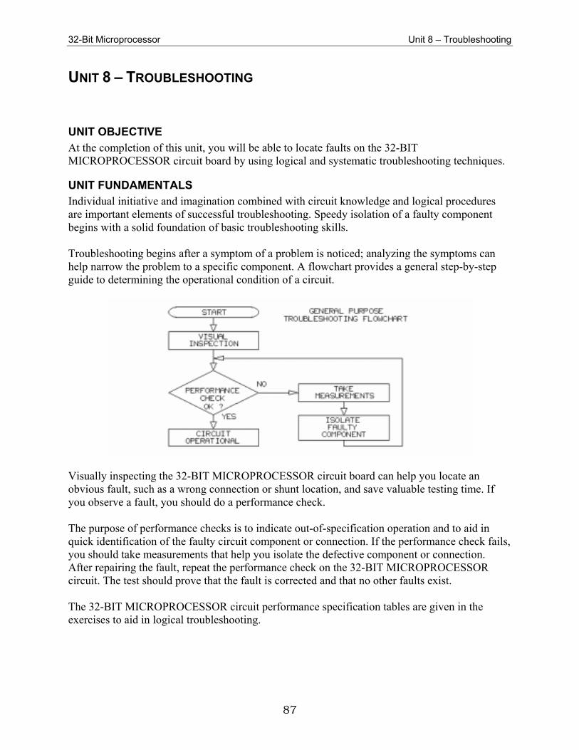
32-Bit Microprocessor Unit 8 – Troubleshooting
87
UNIT 8 – TROUBLESHOOTING
UNIT OBJECTIVE At the completion of this unit, you will be able to locate faults on the 32-BIT MICROPROCESSOR circuit board by using logical and systematic troubleshooting techniques.
UNIT FUNDAMENTALS Individual initiative and imagination combined with circuit knowledge and logical procedures are important elements of successful troubleshooting. Speedy isolation of a faulty component begins with a solid foundation of basic troubleshooting skills. Troubleshooting begins after a symptom of a problem is noticed; analyzing the symptoms can help narrow the problem to a specific component. A flowchart provides a general step-by-step guide to determining the operational condition of a circuit.
Visually inspecting the 32-BIT MICROPROCESSOR circuit board can help you locate an obvious fault, such as a wrong connection or shunt location, and save valuable testing time. If you observe a fault, you should do a performance check. The purpose of performance checks is to indicate out-of-specification operation and to aid in quick identification of the faulty circuit component or connection. If the performance check fails, you should take measurements that help you isolate the defective component or connection. After repairing the fault, repeat the performance check on the 32-BIT MICROPROCESSOR circuit. The test should prove that the fault is corrected and that no other faults exist. The 32-BIT MICROPROCESSOR circuit performance specification tables are given in the exercises to aid in logical troubleshooting.
32-Bit Microprocessor Unit 8 – Troubleshooting
88
NEW TERMS AND WORDS None
EQUIPMENT REQUIRED None
NOTES ______________________________________________________________________________ ______________________________________________________________________________ ______________________________________________________________________________ ______________________________________________________________________________ ______________________________________________________________________________ ______________________________________________________________________________ ______________________________________________________________________________ ______________________________________________________________________________ ______________________________________________________________________________ ______________________________________________________________________________
32-Bit Microprocessor Unit 8 – Troubleshooting
89
Exercise 1 – Troubleshooting Basics
EXERCISE OBJECTIVE When you have completed this exercise, you will be able to troubleshoot the 32-BIT MICROPROCESSOR circuit board by using the guidance provided in this courseware. You will verify your results with an oscilloscope, logic probe, visual observations, and by evaluating the results of test programs.
EXERCISE DISCUSSION
There are three procedures in this exercise. Procedure A - guides you through a circuit performance check. Procedure B - introduces you to a logical and systematic approach to troubleshooting a
fault. Procedure C - allows you to apply this knowledge to a faulty circuit.
A PERFORMANCE SPECIFICATION TABLE is used to tabulate all observed values, normal parameters and a list of measurements that can be performed.
The function key (F7) provides a menu of additional circuit information.
NOTES ______________________________________________________________________________ ______________________________________________________________________________ ______________________________________________________________________________ ______________________________________________________________________________ ______________________________________________________________________________ ______________________________________________________________________________ ______________________________________________________________________________ ______________________________________________________________________________ ______________________________________________________________________________ ______________________________________________________________________________
32-Bit Microprocessor Unit 8 – Troubleshooting
90
Exercise 2 – 32-Bit Microprocessor Troubleshooting
EXERCISE OBJECTIVE When you have completed this exercise, you will be able to troubleshoot the 32-BIT MICROPROCESSOR circuit board by using performance specification tables and you knowledge of microprocessor circuits. You will verify your results with an oscilloscope, logic probe, and visual observations.
EXERCISE DISCUSSION
There are eight separate procedures in this exercise. Each procedure has a fault associated with one of the circuit blocks on the 32-BIT MICROPROCESSOR circuit board.
Faults are inserted after a performance check of the circuit has been completed. A PERFORMANCE SPECIFICATION TABLE is used to tabulate all observed values,
normal parameters, and a list of measurements that can be performed. The function key (F7) provides a menu of additional circuit information.
NOTES ______________________________________________________________________________ ______________________________________________________________________________ ______________________________________________________________________________ ______________________________________________________________________________ ______________________________________________________________________________ ______________________________________________________________________________ ______________________________________________________________________________ ______________________________________________________________________________ ______________________________________________________________________________ ______________________________________________________________________________

32-Bit Microprocessor Unit 9 – Microprocessor Applications (Optional)
91
UNIT 9 – MICROPROCESSOR APPLICATIONS (OPTIONAL)
NOTE: This unit is designed to be used with the MICROPROCESSOR APPLICATIONS board. If you do not have this board, you will not complete this unit.
UNIT OBJECTIVE At the completion of this unit, you will be able to demonstrate practical microprocessor applications by interfacing the 32-BIT MICROPROCESSOR circuit board with the MICROPROCESSOR APPLICATION board. You will verify your results by making observations and taking measurements.
UNIT FUNDAMENTALS
You can use the MICROPROCESSOR APPLICATION board to demonstrate how microprocessors communicate with and control devices in the outside world. The MICROPROCESSOR APPLICATION board includes motor control and temperature control circuits. You can interface to a microprocessor board via I/O control lines and the DACOUT and ADCIN signals. The two application circuit blocks are the DC MOTOR CONTROLLER and the TEMPERATURE CONTROLLER blocks. The POWER and CONTROL circuit blocks contain headers to connect this board to the 32-BIT MICROPROCESSOR circuit board. The TEST POINTS circuit block contains a header whose pins are test points used to monitor the digital and analog signals exchanged between the two circuit boards.

32-Bit Microprocessor Unit 9 – Microprocessor Applications (Optional)
92
The 8-pin header in the POWER circuit block connects to the 32-BIT MICROPROCESSOR circuit board with a ribbon cable assembly. This header supplies +5V, +12V, and -12V to the analog and digital circuitry on the MICROPROCESSOR APPLICATION BOARD. Separate analog and digital grounds are included to maximize noise immunity. The ground connections are accessible in the TEST POINTS circuit block.
The header in the CONTROL circuit block also connects to the 32-BIT MICROPROCESSOR circuit board with a ribbon cable assembly. This connection includes three I/O port lines as well as the DACOUT and ADCIN signals.
The signals from the CONTROL cable are accessible on the 20-pin header in the TEST POINTS circuit block. Depending on the signal type, you can monitor these points with an oscilloscope, logic probe, or voltmeter.

32-Bit Microprocessor Unit 9 – Microprocessor Applications (Optional)
93
The DC MOTOR CONTROLLER circuit block has a motor whose speed and direction of rotation can be controlled by the microprocessor board. The microprocessor board can drive the motor in one of two ways, as determined by a shunt on the MOT header. When the shunt is in the SWT (switched) position, the microprocessor uses a single output bit in the PPI to turn the motor fully on (logic 1) or fully off (logic 0). In the SWT mode, the motor always rotates counter-clockwise (CCW). When the MOT shunt is in the LIN (linear) position, the motor speed and direction are determined by an analog voltage sent by the micro-processor via the DACOUT line. The motor speed is proportional to the DACOUT voltage, and the direction of rotation depends on whether the applied voltage is positive or negative. The DAC has a unipolar 0-10V output. However, the DC MOTOR CONTROLLER circuit block converts the DAC voltage to a bipolar -3V to +3V range. In the LIN mode, the polarity of this voltage determines motor direction, and the magnitude of the voltage determines speed. Mounted on the motor's shaft are a fan blade and an encoder disc. One function that these components have is to make it easier for you to see the rotation of the motor shaft.
This side view shows the motor, fan, encoder disc, and an optical interrupter located beneath the disc. The fan is located so that its air flow can cool the heater in the TEMPERATURE CONTROLLER circuit block.

32-Bit Microprocessor Unit 9 – Microprocessor Applications (Optional)
94
The encoder disc has several black marks around its perimeter. The disc is positioned so that as it rotates, it passes through the optical interrupter. Each time a black mark passes through the optical interrupter, a digital pulse is generated. The encoder disc and optical interrupter provide a method of sensing the motor speed and feeding it back to the microprocessor.
The TEMPERATURE CONTROLLER cirucit block uses two temperature transducers whose output current is a function of their temperature. One transducer is thermally bonded to a resistor that is used as a heater. The microprocessor uses an output port bit to turn the heater on or off, and a red LED indicates the heater status. The second transducer is located away from the heater and is used as a room-temperature reference. An op amp circuit generates a voltage that is a function of the difference of the two outputs. The differential voltage represents the difference between the heater temperature and room temperature. The microprocessor can also send an analog value to the TEMPERATURE CONTROLLER circuit block via the DACOUT line. The DACOUT value serves as a reference voltage in the op amp circuit. The ADC header in the TEMPERATURE CONTROLLER circuit block determines whether the motor voltage or the differential temperature transducer voltage is fed back to the microprocessor.
32-Bit Microprocessor Unit 9 – Microprocessor Applications (Optional)
95
NEW TERMS AND WORDS optical interrupter - an optoelectronic device with an LED and a phototransistor located on opposite sides of an open slot. An object passing through the slot can interrupt the light beam and cause the optical interrupter to generate output pulses. temperature transducers - a transducer whose output is a function of its temperature. open-loop temperature control - a form of temperature control by which a heater is activated but no temperature information is fed back to the controlling device. closed-loop temperature control - a form of temperature control by which a heater is activated and its temperature is fed back to the controlling device in order to regulate temperature. set point - the desired temperature at which a temperature controller is to regulate temperature.
EQUIPMENT REQUIRED FACET base unit MICROPROCESSOR APPLICATION BOARD Multimeter Oscilloscope, dual trace 32-BIT MICROPROCESSOR circuit board
NOTES ______________________________________________________________________________ ______________________________________________________________________________ ______________________________________________________________________________ ______________________________________________________________________________ ______________________________________________________________________________ ______________________________________________________________________________ ______________________________________________________________________________ ______________________________________________________________________________ ______________________________________________________________________________ ______________________________________________________________________________
32-Bit Microprocessor Unit 9 – Microprocessor Applications (Optional)
96
Exercise 1 – Application Board Familiarization
EXERCISE OBJECTIVE When you have completed this exercise, you will be able to explain the function of each circuit block on the MICROPROCESSOR APPLICATION board.
EXERCISE DISCUSSION
Three digital I/O lines (PC0, PB0, and PB7) from the 32-BIT MICROPROCESSOR circuit board are used for control signals.
The microprocessor board uses output bit PB0 to switch the heater resistor on and off for temperature control applications. Output bit PB7 turns the motor on or off.
The encoder output signal is fed back to the microprocessor board via input line PC0. The microprocessor board generates an analog voltage at DACOUT to control motor speed
and direction when LIN mode is selected on the MOT header. The motor voltage is also connected to comparators which drive LEDs that indicate CW or
CCW motor direction. The microprocessor board can read the analog voltage from the TEMPERATURE
CONTROLLER or DC MOTOR CONTROLLER circuit block via the ADCIN line depending on the position of the ADC shunt.

32-Bit Microprocessor Unit 9 – Microprocessor Applications (Optional)
97
NOTES ______________________________________________________________________________ ______________________________________________________________________________ ______________________________________________________________________________ ______________________________________________________________________________ ______________________________________________________________________________ ______________________________________________________________________________ ______________________________________________________________________________ ______________________________________________________________________________ ______________________________________________________________________________ ______________________________________________________________________________
32-Bit Microprocessor Unit 9 – Microprocessor Applications (Optional)
98
Exercise 2 – DC Motor Control
EXERCISE OBJECTIVE When you have completed this exercise, you will be able to explain and demonstrate how a microprocessor can control the speed and direction of rotation of a small dc motor.
EXERCISE DISCUSSION
The motor operates from about -3 to +3 Vdc. Direction of rotation is CW for positive voltages and CCW for negative voltages. The motor is off if 0V is applied.
When the MOT shunt is in the SWT position, op amp (U5B) drives the motor. The op amp is controlled by I/O bit PB7. The op amp output is 0V for a low PB7 logic level
and -3V for a high PB7 logic level. PB7 can be used as a simple on/off control for applications.
Alternatively, the microprocessor can switch PB7 on and off continuously and vary the duty cycle to control the motor speed.
When the MOT shunt is in the LIN position, the motor voltage is supplied by op amp (U5A). U5A is driven by the DACOUT signal, which has a 0-10 Vdc range.
The op amp scales and shifts the DAC voltage range into a bipolar range of about -3 to +3 Vdc. At 0V, the motor is stopped.
When a positive voltage is applied, the motor runs CW and its speed increases as the voltage increases. When a negative voltage is applied, the motor runs CCW, and its speed increases as the voltage goes more negative.
The motor is also connected to two comparator circuits that drive LEDs to indicate motor direction.
The microprocessor board can read the motor voltage by sampling the ADCIN line when the ADC shunt is in the MOT position.
The microprocessor board can determine motor speed by counting the pulses from the optical interrupter.
U4A and U4B buffer the phototransistor output and drive the PC0 input to the microprocessor board.
The optical interrupter outputs five pulses for each revolution of the motor shaft. The microprocessor can count the number of pulses that occur in one second and divide by five to determine the motor speed in revolutions per second.

32-Bit Microprocessor Unit 9 – Microprocessor Applications (Optional)
99
NOTES ______________________________________________________________________________ ______________________________________________________________________________ ______________________________________________________________________________ ______________________________________________________________________________ ______________________________________________________________________________ ______________________________________________________________________________ ______________________________________________________________________________ ______________________________________________________________________________ ______________________________________________________________________________ ______________________________________________________________________________

32-Bit Microprocessor Unit 9 – Microprocessor Applications (Optional)
100
Exercise 3 – Temperature Control
EXERCISE OBJECTIVE When you have completed this exercise, you will be able to explain and demonstrate the use of a microprocessor in open and closed-loop temperature control applications. You will verify your results by loading and executing simple programs, making observations, and taking measurements.
DISCUSSION
Output bit PB0 drives inverting buffers U4E and U4D, which in turn switch transistor Q1 on (PBO = 1) and off (PB0 = 0).
When Q1 is on, current flows through the 33 resistor, causing it to heat up. The heater resistor is thermally bonded to U3, which is a current-output temperature
transducer. U2 is a second temperature transducer located away from the heater and used as a room-
temperature reference. The (+) output of U3 is connected to the (-) output of U2. The current at the junction of the
two devices is therefore the difference of the two output currents. The U2/U3 junction is connected to the inverting input of op amp U1A. The current into this input is multiplied by the feedback resistance to generate an output
voltage proportional to the temperature difference. The non-inverting input is connected to a voltage divider that is referenced to DACOUT. For temperature control applications on your circuit board, DACOUT is used as a precision
voltage reference. The input value is always FFH, which gives an output voltage of about 10V (0.039 x 255 = 9.945V).
The +5V from the voltage divider provides an offset. When both transducers are at room temperature (net transducer current = zero), the op amp output is about +5V.
The op amp output drives the ADCIN line when the ADC shunt is in the TEMP position. This output voltage is a function of the difference between room temperature and the heater temperature.
The two ways the microprocessor can control temperature are: open-loop temperature control or closed-loop temperature control.
In open-loop temperature control, the CPU sets PB0 to turn on the heater. This method does not regulate the heater temperature.
In closed-loop temperature control, the CPU sets PB0 to turn on the heater but, the heater temperature is fed back to the CPU in the form of a voltage via ADCIN. The ADCIN voltage level is read by the CPU and used to determine if, based on a programmed set point, the heater must be turned on or off.

32-Bit Microprocessor Unit 9 – Microprocessor Applications (Optional)
101
NOTES ______________________________________________________________________________ ______________________________________________________________________________ ______________________________________________________________________________ ______________________________________________________________________________ ______________________________________________________________________________ ______________________________________________________________________________ ______________________________________________________________________________ ______________________________________________________________________________ ______________________________________________________________________________ ______________________________________________________________________________

32-Bit Microprocessor Unit 9 – Microprocessor Applications (Optional)
102

APPENDIX A – SAFETY
Safety is everyone’s responsibility. All must cooperate to create the safest possible working environment. Students must be reminded of the potential for harm, given common sense safety rules, and instructed to follow the electrical safety rules. Any environment can be hazardous when it is unfamiliar. The FACET computer-based laboratory may be a new environment to some students. Instruct students in the proper use of the FACET equipment and explain what behavior is expected of them in this laboratory. It is up to the instructor to provide the necessary introduction to the learning environment and the equipment. This task will prevent injury to both student and equipment. The voltage and current used in the FACET Computer-Based Laboratory are, in themselves, harmless to the normal, healthy person. However, an electrical shock coming as a surprise will be uncomfortable and may cause a reaction that could create injury. The students should be made aware of the following electrical safety rules. 1. Turn off the power before working on a circuit. 2. Always confirm that the circuit is wired correctly before turning on the power. If required,
have your instructor check your circuit wiring. 3. Perform the experiments as you are instructed: do not deviate from the documentation. 4. Never touch “live” wires with your bare hands or with tools. 5. Always hold test leads by their insulated areas. 6. Be aware that some components can become very hot during operation. (However, this is not
a normal condition for your FACET course equipment.) Always allow time for the components to cool before proceeding to touch or remove them from the circuit.
7. Do not work without supervision. Be sure someone is nearby to shut off the power and provide first aid in case of an accident.
8. Remove power cords by the plug, not by pulling on the cord. Check for cracked or broken insulation on the cord.

THIS THIS


![DESIGN OF 32-BIT MICROCONTROLLER … has 32-bit RICS microprocessor, data cache, instruction cache, FLASH controller, SDRAM controller, DMA (dynamic memory access), UART [7] (universal](https://static.fdocuments.net/doc/165x107/5adcdd157f8b9a9d4d8c5818/design-of-32-bit-microcontroller-has-32-bit-rics-microprocessor-data-cache.jpg)


