31 2026 25 21 1516 11 10 6 5 0 shamt funct 31 2026 25 21 1516...
72
The MIPS instruction set architecture The MIPS has a 32 bit architecture, with 32 bit instructions, a 32 bit data word, and 32 bit addresses. It has 32 addressable internal registers requiring a 5 bit register ad- dress. Register 0 always has the the constant value 0. Addresses are for individual bytes (8 bits) but instructions must have addresses which are a multiple of 4. This is usually stated as “in- structions must be word aligned in memory.” There are three basic instruction types with the following formats: shamt funct op rs rt rd 0 31 20 21 15 16 11 10 65 25 26 I-type (immediate) op rs rt 0 31 20 21 15 16 25 26 immediate R-type (register) J-type (jump) op 0 31 25 26 target 6 bits 6 bits 5 bits 5 bits 5 bits 5 bits 5 bits 5 bits 6 bits 16 bits 26 bits 6 bits All op codes are 6 bits. All register addresses are 5 bits. 32
Transcript of 31 2026 25 21 1516 11 10 6 5 0 shamt funct 31 2026 25 21 1516...

The MIPS instruction set architecture
The MIPS has a 32 bit architecture, with 32 bit instructions, a 32
bit data word, and 32 bit addresses.
It has 32 addressable internal registers requiring a 5 bit register ad-
dress. Register 0 always has the the constant value 0.
Addresses are for individual bytes (8 bits) but instructions must have
addresses which are a multiple of 4. This is usually stated as “in-
structions must be word aligned in memory.”
There are three basic instruction types with the following formats:
shamt functop rs rt rd031 2021 1516 11 10 6 52526
I−type (immediate)
op rs rt031 2021 15162526
immediate
R−type (register)
J−type (jump)
op031 2526
target
6 bits 6 bits5 bits5 bits5 bits5 bits
5 bits 5 bits6 bits 16 bits
26 bits6 bits
All op codes are 6 bits.
All register addresses are 5 bits.
32

shamt functop rs rt rd031 2021 1516 11 10 6 52526
R−type (register)
The R-type instructions are 3 operand arithmetic and logic instruc-
tions, where the operands are contained in the registers indicated by
rs, rt, and rd.
For all R-type instructions, the op field is 000000.
The funct field selects the particular type of operation for R-type
operations.
The shamt field determines the number of bits to be shifted (0 to
31).
These instructions perform the following:
R[rd] ← R[rs] op R[rt]
Following are examples of R-type instructions:
Instruction Example Meaning
add add $s1, $s2, $s3 $s1 = $s2 + $s3
add unsigned addu $s1, $s2, $s3 $s1 = $s2 + $s3
subtract sub $s1, $s2, $s3 $s1 = $s2 - $s3
subtract unsigned subu $s1, $s2, $s3 $s1 = $s2 - $s3
and and $s1, $s2, $s3 $s1 = $s2 & $s3
or or $s1, $s2, $s3 $s1 = $s2 | $s3
33

I−type (immediate)
op rs rt031 2021 15162526
immediate
The 16 bit immediate field contains a data constant for an arithmetic
or logical operation, or an address offset for a branch instruction.
This type of branch is called a relative branch.
Following are examples of I-type instructions of type:
R[rt] ← R[rs] op imm
Instruction Example Meaning
add addi $s1, $s2, imm $s1 = $s2 + imm
add unsigned addiu $s1, $s2, imm $s1 = $s2 + imm
subtract subi $s1, $s2, imm $s1 = $s2 - imm
and andi $s1, $s2, imm $s1 = $s2 & imm
Another I-type instruction is the branch instruction.
Examples of this are:
Instruction Example Meaning
branch on equal beq $s1, $s2, imm if $s1 == $s2 go to
PC + 4 + (4 × imm)
branch on not equal bne $s1, $s2, imm if $s1 != $s2 go to
PC + 4 + (4 × imm)
Why is the imm field multiplied by 4 here?
34

J−type (jump)
op031 2526
target
The J-type instructions are all jump instructions.
The two we will discuss are the following:
Instruction Example Meaning
jump j target go to address 4 × target : PC[28:31]
jump and link jal target $31 = PC + 4;
go to address 4 × target : PC[28:31]
Why is the PC incremented by 4?
Why is the target field multiplied by 4?
Recall that the MIPS processor addresses data at the byte level, but
instructions are addressed at the word level.
Moreover, all instructions must be aligned on a word boundary (an
integer multiple of 4 bytes).
Therefore, the next instruction is 4 byte addresses from the current
instruction.
Since jumps must have an instruction as target, shifting the target
address by 2 bits (which is the same as multiplying by 4) allows the
instruction to specify larger jumps.
Note that the jump instruction cannot span (jump across) all of
memory.
35

There are a few more interesting instructions, for comparison, and
memory access:
R-type instructions:
Instruction Example Meaning
set less than slt $s1, $s2, $s3 if ($s2 < $s3), $s1=1;
else $s1=0
jump register jr $ra go to $ra
set less than also has an unsigned form.
jump register is typically used to return from a subprogram.
I-type instructions:
Instruction Example Meaning
set less than slti $s1, $s2, imm if ($s2 < imm), $s1=1;
immediate else $s1=0
load word lw $s1, imm($s2) $s1 = Memory[$s2 + imm]
store word sw $s1, imm($s2) Memory[$s2 + imm] = $s1
load word and store word are the only instructions that access
memory directly.
Because data must be explicitly loaded before it is operated on, and
explicitly stored afterwards, the MIPS is said to be a load/store
architecture.
This is often considered to be an essential feature of a reduced in-
struction set architecture (RISC).
36

The MIPS assembly language
The previous diagrams showed examples of code in a general form
which is commonly used as a simple kind of language for a processor
— a language in which each line in the code corresponds to a single
instruction in the language understood by the machine.
For example,
add $1, $2, $3
means take add together the contents of registers $2 and $3 and
store the result in register $1.
We call this type of language an assembly language.
The language of the machine itself, called the machine language,
consists only of 0’s and 1’s — a binary code.
The machine language instruction corresponding to the previous in-
struction (with the different fields identified) is:
031 2021 1516 11 10 6 52526
rd shamt functrtrsop000000 00010 00011 00001 00000 100000
There are usually programs, called assemblers, to translate the more
human readable assembly code to machine language.
37

MIPS memory usage
MIPS systems typically divided memory into three parts, called seg-
ments.
These segments are the text segment which contains the program’s
instructions, the data segment, which contains the program’s data,
and the stack segment which contains the return addresses for func-
tion calls, and also contains register values which are to be saved and
restored. It may also contain local variables.
��������������������������������
��������������������������������
10000000
7fffffff
Reserved
Static data
Dynamic data
stackStack segment
Data segment
Text segment
400000hex
hex
hex
The data segment is divided into 2 parts, the lower part for static
data (with size known at compile time) and the upper part, which
can grow, upward, for dynamic data structures.
The stack segment varies in size during the execution of a program,
as functions are called and returned from.
It starts at the top of memory and grows down.
44

MIPS register names and conventions about their use
Register Name Number Usage
zero 0 Constant 0
at 1 Reserved for assembler
v0 2 Expression evaluation and
v1 3 results of a function
a0 4 Argument 1
a1 5 Argument 2
a2 6 Argument 3
a3 7 Argument 4
t0 8 Temporary (not preserved across call)
t1 9 Temporary (not preserved across call)
t2 10 Temporary (not preserved across call)
t3 11 Temporary (not preserved across call)
t4 12 Temporary (not preserved across call)
t5 13 Temporary (not preserved across call)
t6 14 Temporary (not preserved across call)
t7 15 Temporary (not preserved across call)
s0 16 Saved temporary (preserved across call)
s1 17 Saved temporary (preserved across call)
s2 18 Saved temporary (preserved across call)
s3 19 Saved temporary (preserved across call)
s4 20 Saved temporary (preserved across call)
s5 21 Saved temporary (preserved across call)
s6 22 Saved temporary (preserved across call)
s7 23 Saved temporary (preserved across call)
t8 24 Temporary (not preserved across call)
t9 25 Temporary (not preserved across call)
k0 26 Reserved for OS kernel
k1 27 Reserved for OS kernel
gp 28 Pointer to global area
sp 29 Stack pointer
fp 30 Frame pointer
ra 31 Return address (used by function call)
54

Presently, we are interested in the CPU only, which we concluded
would have a structure similar to the following:
AddressGeneratorPCU
PC
GeneralRegisters
and/orAccumulator
Instructiondecode and
ControlUnitALU
MDR
MAR
The memory address register (MAR) and memory data register(MDR)
are the interface to memory.
The ALU and register file are the core of the data path.
The program control unit (PCU) fetches instructions and data, and
handles branches and jumps.
The instruction decode unit (IDU) is the control unit for the proces-
sor.
188

The “building blocks”
We have already designed many of the major components for the
processor, or have at least identified how they could be implemented.
For example, we have already designed an ALU, a data register, and
a register file.
A controller is merely a state machine, and we can implement one
using, say, a PLA, after identifying the required states and transi-
tions.
Following are some of the combinational logic components we will
use:
✲ ✲OP S❅
❅❅
❅ ◗◗✑✑ ��
��
❄❄
❅❅
❅❅ ◗◗✑✑ �
��
�
❄❄
❄
��
❄ ❄ ❄
��
��
��
��
��
❄❄
❄
Adder
Sum Carry
Adder
ALU
Result Zero
ALU
Multiplexor
A
32
B
32
A
32
B
32
32 32
MUX
A B
Y
Note that the diagram highlights the control signals (OP and S).
189

Following are some of the register components we will use:
✂✂❇❇✂✂❇❇
✂✂❇❇
Write enable
ClockClock
Write enable
Clock
Registerfile
✲ ✲ ✲ ✲��
��
��
��
✲
✲
✲
✲
✲
✲
��
��
��
��
��
��
32PC
323230
RegisterCounter
Data outData in
Registers
Read
RegisterWrite
register 2
register 1Read
Writedata
data 1Read
Readdata 2
32
32
5
5
5
32
Note that the registers have a write enable input as well as a clock
input. This input must be asserted in order for the register to be
written.
We have already seen how to construct a register file from simple D
registers.
190

Timing considerations
In a single-cycle implementation of the processor, a single instruction
(e.g., add) may require that a register be read from and written into
in the same clock period. In order to accomplish this, the register
file (and other register elements) must be edge triggered.
This can be done by using edge triggered elements directly, or by
using a master-slave arrangement similar to one we saw earlier:
❞❍❍✟✟
s
D Q D Q
>>
master slave
Another observation about a single cycle processor — the memory
for instructions must be different from the memory for data, because
both must be addressed in the same cycle. Therefore, there must be
two memories; one for instructions, and one for data.
MemoryData
Readdata
Instruction[31-0]
Writedata
✲
✁✁ ✲
✁✁✲
✁✁
✲
✲
✁✁
✁✁
32
Address32
Read
MemoryInstruction
32
Address32
32
MemWr
MemRd
Data memory Instruction memory
191

The MIPS instruction set:
Following is the MIPS instruction format:
shamt functop rs rt rd031 2021 1516 11 10 6 52526
I-type (immediate)
op rs rt031 2021 15162526
immediate
R-type (register)
J-type (jump)
op031 2526
target
6 bits 6 bits5 bits5 bits5 bits5 bits
5 bits 5 bits6 bits 16 bits
26 bits6 bits
We will develop an implementation of a very basic processor having
the instructions:
R-type instructions add, sub, and, or, slt
I-type instructions addi, lw, sw, beq
J-type instructions j
Later, we will add additional instructions.
192

Steps in designing a processor
• Express the instruction architecture in a Register Transfer Lan-
guage (RTL)
• From the RTL description of each instruction, determine
– the required datapath components
– the datapath interconnections
• Determine the control signals required to enable the datapath
elements in the appropriate sequence for each instruction
• Design the control logic required to generate the appropriate
control signals at the correct time
193

A Register Transfer Language description of some op-
erations:
The ADD instruction
add rd, rs, rt
• mem[PC] Fetch the instruction from memory
• R[rd] ← R[rs] + R[rt] Set register rd to the value of the
sum of the contents of registers rs
and rt
• PC ← PC + 4 calculate the address of the next in-
struction
All other R-type instructions will be similar.
The addi instruction
addi rs, rt, imm16
• mem[PC] Fetch the instruction from memory
• R[rt] ← R[rs] +
SignExt(imm16)
Set register rt to the value of
the sum of the contents of register
rs and the immediate data word
imm16
• PC ← PC + 4 calculate the address of the next in-
struction
All immediate arithmetic and logical instructions will be similar.
194

The load instruction
lw rs, rt, imm16
• mem[PC] Fetch the instruction from memory
• Addr ← R[rs] +
SignExt(imm16)
Set memory address to the value of
the sum of the contents of register
rs and the immediate data word
imm16
• R[rt] ← Mem[Addr] load the data at address Addr into
register rt
• PC ← PC + 4 calculate the address of the next in-
struction
The store instruction
sw rs, rt, imm16
• mem[PC] Fetch the instruction from memory
• Addr ← R[rs] +
SignExt(imm16)
Set memory address to the value of
the sum of the contents of register
rs and the immediate data word
imm16
• Mem[Addr] ← R[rt] store the data from register rt into
memory at address Addr
• PC ← PC + 4 calculate the address of the next in-
struction
195

The branch instruction
beq rs, rt, imm16
• mem[PC] Fetch the instruction from memory
• Cond ← R[rs] - R[rt] Evaluate the branch condition
• if (Cond eq 0)
PC ← PC + 4 +
(SignExt(imm16) × 4)
calculate the address of the next in-
struction
• else PC ← PC + 4
The jump instruction
j target target is a memory address
• mem[PC] Fetch the instruction from memory
• PC ← PC + 4 increment PC by 4
• PC<31:2> ← PC<31:28> replace low order 28 bits with
concat I<25:0> << 2 the low order 26 bits from the in-
struction left shifted by 2
196

The Instruction Fetch Unit
Note that all instructions require that the PC be incremented.
We will design a datapath which performs this function — the In-
struction Fetch Unit.
Its operation is described by the following:
• mem[PC] Fetch the instruction from memory
• PC ← PC + 4 Increment the PC
Instruction[31−0]
MemoryInstruction
addressReadPC
Add
4
Note that this does not yet handle branches or jumps.
Since it is the same for all instructions, when describing individual
instructions this component will normally be omitted.
197

Datapath for R-type instructions
• R[rd] ← R[rs] op R[rt] Example: add rd, rs, rt
Recall that this instruction type has the following format:
R−type (register)
shamt functop rs rt rd031 2021 1516 11 10 6 52526
6 bits 5 bits 5 bits 5 bits 6 bits5 bits
The datapath contains the 32 bit register file and and ALU capable
of performing all the required arithmetic and logic functions.
dataWrite
RegisterWrite
ReadRegister 2
Register 1Read
Readdata 1
Readdata 2
ALU Result
32
Registers
32
32
rs
rt
rd
clk
ALUCtrRegWr
Inst[15−11]
Inst[20−16]
Inst[25−21]
BusA
BusB
Inst
Note that the register is read from and written to at the “same
time.” This implies that the register’s memory elements must be
edge triggered, or are read and written on different clock phases, to
allow the arithmetic operation to complete before the data is written
in the register.
198

This datapath contains everything required to implement the re-
quired instructions add, sub, and, or, slt. All that is required
is that the appropriate values be provided for the ALUCtr input for
the required operation.
The register operands in the instruction field determine the regis-
ters which are read from and written to, and the funct field of the
instruction determine which particular ALU operation is executed.
Recalling the control inputs for the ALU seen earlier, the values for
the control input are:
ALU control lines Function
000 and
001 or
010 add
110 subtract
111 set on less than
A control unit for the processor will be designed later.
It will set all the required control signals for each instruction, de-
pending both on the particular instruction being executed (the op
code) and, for r-type instructions, the funct field.
199

Datapath for Immediate arithmetic and logical instruc-
tions
• R[rt] ← R[rs] op imm16 Example: addi rt, rs, imm16
Recall that this instruction type has the following format:
I−type (immediate)
op rs rt031 2021 15162526
immediate6 bits 5 bits 5 bits 16 bits
The main difference between this and an r-type instruction is that
here one operand is taken from the instruction, and sign extended (for
signed data) or zero extended (for logical and unsigned operations.)
RegDst ALUSrc
dataWrite
RegisterWrite
ReadRegister 2
Register 1Read
Readdata 1
Readdata 2
ALURegisters
Inst[20−16]
Inst[25−21]
32
extend
16
imm16
rs
rt
ALUCtr
BusB
BusA
32
32
Clk
RegWr
MUX
0
1MUX
0
1
Inst[15−0]
Inst[15−11]
Sign
Note the use of MUX’s (with control inputs) to add functionality.
200

Datapath for the Load instruction
lw rt, rs, imm16
• Addr ← R[rs] +
SignExt(imm16)
Calculate the memory address
• R[rt] ← Mem[Addr] load the data into register rt
This is also an immediate type instruction:
I−type (immediate)
op rs rt031 2021 15162526
immediate6 bits 5 bits 5 bits 16 bits
Clk
RegWr
AluSrc AluCtr
RegDst
MemRd
MemtoReg
MUX
0
1
dataWrite
Readdata
MemoryData
MUX
0
1dataWrite
RegisterWrite
ReadRegister 2
Register 1Read
Readdata 1
Readdata 2
extendSign
ALUAddress
Registers
Inst[20−16]
Inst[25−21]
Inst[15−11]
16 32Inst[15−0]
32 MU
1
0X
32
BusB
BusA
32
32
32
Data In
201

Datapath for the Store instruction
sw rt, rs, imm16
• Addr ← R[rs] +
SignExt(imm16)
Calculate the memory address
• Mem[Addr] ← R[rt] Store the data from register rt to
memory
This is also an immediate type instruction:
I−type (immediate)
op rs rt031 2021 15162526
immediate6 bits 5 bits 5 bits 16 bits
MUX
0
1
dataWrite
Readdata
MemoryData
MUX
0
1dataWrite
RegisterWrite
ReadRegister 2
Register 1Read
Readdata 1
Readdata 2
extendSign
ALUAddress
Registers
Inst[20−16]
Inst[25−21]
Inst[15−11]
16 32
Clk
Inst[15−0]
RegWr
AluSrc AluCtr MemWr
MemtoReg
32
RegDst
32
MemRd
BusA
BusB
Data In
32
32
MUX
1
0
202

Datapath for the Branch instruction
beq rt, rs, imm16
• Cond ← R[rs] - R[rt] Calculate the branch condition
• if (Cond eq 0)
PC ← PC + 4 +
(SignExt(imm16) × 4)
calculate the address of the next in-
struction
• else PC ← PC + 4
This is also an immediate type instruction.
In the load and store instructions, the ALU was used to calculate
the address for data memory.
It is possible to do this for the branch instructions as well, but it
would require first performing the comparison using the ALU, and
then using the ALU to calculate the address.
This would require two clock periods, in order to sequence the oper-
ations correctly.
A faster implementation would be to provide another adder to im-
plement the address calculation. This is what we will do, for the
present example.
203

RegWr
RegDst
Zero
ALUSrc ALUCtr
BranchPCSrc
MUX
0
1dataWrite
RegisterWrite
ReadRegister 2
Register 1Read
Readdata 1
Readdata 2
extendSign
Instruction[31−0]
MemoryInstruction
addressReadPC
Add
4
Registers
Inst[20−16]
Inst[25−21]
Inst[15−11]
16 32Inst[15−0]
ALU
Add
MUX
0
1
Shiftleft 2
MUX
0
1
204

Datapath for the Jump instruction
j target
• PC<31:2> ← PC<31:28>
concat target<25:0>
Calculate the jump address by con-
catenating the high order 4 bits of
the PC with the target address
Here, the address calculation is just obtained from the high order 4
bits of the PC and the 26 bits (shifted left by 2 bits to make 28) of
the target address.
The additions to the datapath are straightforward.
6 bits
J−type (jump)
op031 2526
target address26 bits
205

RegWr
RegDst
Zero
ALUSrc ALUCtr
Branch Jump
PCSrc
MUX
0
1dataWrite
RegisterWrite
ReadRegister 2
Register 1Read
Readdata 1
Readdata 2
extendSign
Instruction[31−0]
MemoryInstruction
addressReadPC
Add
4
Shiftleft 2
MUX
0
1
Registers
Inst[20−16]
Inst[25−21]
Inst[15−11]
16 32Inst[15−0]
ALU
Add
MUX
0
1
MUX
1
0
Shiftleft 2
206

Putting it together
The datapath was shown in segments, some of which built on each
other.
Required control signals were identified, and all that remains is to:
1. Combine the datapath elements
2. Design the appropriate control signals
Combining the datapath elements is rather straightforward, since
we have mainly built up the datapath by adding functionality to
accommodate the different instruction types.
When two paths are required, we have implemented both and used
multiplexors to choose the appropriate results.
The required control signals are mainly the inputs for those MUX’s
and the signals required by the ALU.
The next slide shows the combined data path, and the required con-
trol signals.
The actual control logic is yet to be designed.
207

controlALU
MemRead
MemtoReg
MemWrite
ALUSrc
RegWrite
ALUOpInst [31−26]
RegDst
Branch
Control
Jump PCSrc
Inst[5−0]
MUX
0
1
Shiftleft 2
extendSign
Shiftleft 2 M
UX
0
1
MUX
1
0
dataWrite
RegisterWrite
ReadRegister 2
Register 1Read
Readdata 1
Readdata 2
RegistersMUX
0
1
Instruction[31−0]
MemoryInstruction
addressRead
Add
4
PC
dataWrite
Readdata
MemoryData
Address
MUX
1
0
Add
Zero
16 32
Inst[25−0]
26 28
PC+4[31−28]
Jump address[31−0]
funct
32
32
ALU
32
32
32
32
BusA
BusB
Inst[20−16]
Inst[15−11]
rt
rd
rsInst[25−21]
Inst[15−0]
32
208

Designing the control logic
The control logic depends on the details of the devices in the control
path, and on the individual bits in the op code for the instructions.
The arithmetic and logic operations for the r-type instructions also
depend on the funct field of the instruction.
The datapath elements we have used are:
• a 32 bit ALU with an output indicating if the result is zero
• adders
• MUX’s (2 line to 1-line)
• a 32 register × 32 bits/register register file
• individual 32 bit registers
• a sign extender
• instruction memory
• data memory
209

The ALU — a single bit
+0
1
0
1
3
2
Carryin
OperationBinvert
a
b
Less
Result
Carryout
Note that there are three control bits; the single bit Binvert, and
the two bit input to the MUX, labeled Operation.
The ALU performs the operations and, or, add, and subtract.
210

The 32 bit ALU
a0b0
CarryinALU0Less
CarryOut
Result0
CarryinALU31
a31
0b31
Less Overflow
zero
Operation
CarryinALU1Less
CarryOut
a1
0b1
Result1
Result31
Set
Binvert
CarryinALU2Less
CarryOut
a2
0b2
Result2
ALU control lines Function
000 and
001 or
010 add
110 subtract
111 set on less than
211

We will design the control logic to implement the following instruc-
tions (others can be added similarly):
Name Op-code
Op5 Op4 Op3 Op2 Op1 Op0
R-format 0 0 0 0 0 0
lw 1 0 0 0 1 1
sw 1 0 1 0 1 1
beq 0 0 0 1 0 0
j 0 0 0 0 1 0
Note that we have omitted the immediate arithmetic and logic func-
tions.
The funct field will also have to be decoded to produce the required
control signals for the ALU.
A separate decoder will be used for the main control signals and the
ALU control. This approach is sometimes called local decoding. Its
main advantage is in reducing the size of the main controller.
212

The control signals
The signals required to control the datapath are the following:
• Jump — set to 1 for a jump instruction
• Branch — set to 1 for a branch instruction
• MemtoReg — set to 1 for a load instruction
• ALUSrc — set to 0 for r-type instructions, and 1 for instructions
using immediate data in the ALU (beq requires this set to 0)
• RegDst — set to 1 for r-type instructions, and 0 for immediate
instructions
• MemRead — set to 1 for a load instruction
• MemWrite — set to 1 for a store instruction
• RegWrite — set to 1 for any instruction writing to a register
• ALUOp (k bits) — encodes ALU operations except for r-type
operations, which are encoded by the funct field
For the instructions we are implementing, ALUOp can be encoded
using 2 bits as follows:
ALUOp[1] ALUOp[0] Instruction
0 0 memory operations (load, store)
0 1 beq
1 0 r-type operations
213

The following tables show the required values for the control signals
as a function of the instruction op codes:
Instruction Op-code RegDst ALUSrc MemtoReg Reg
Write
r-type 0 0 0 0 0 0 1 0 0 1
lw 1 0 0 0 1 1 0 1 1 1
sw 1 0 1 0 1 1 x 1 x 0
beq 0 0 0 1 0 0 x 0 x 0
j 0 0 0 0 1 0 x x x 0
Instruction Op-code Mem Mem Branch ALUOp[1:0] Jump
Read Write
r-type 0 0 0 0 0 0 0 0 0 1 0 0
lw 1 0 0 0 1 1 1 0 0 0 0 0
sw 1 0 1 0 1 1 0 1 0 0 0 0
beq 0 0 0 1 0 0 0 0 1 0 1 0
j 0 0 0 0 1 0 0 0 0 x x 1
This is all that is required to implement the control signals; each
control signal can be expressed as a function of the op-code bits.
For example,
RegDst = Op5 · Op4 · Op3 · Op2 · Op1 · Op0
ALUSrc = Op5 · Op4 · Op2 · Op1 · Op0
All that remains is to design the control for the ALU.
214

The ALU control
The inputs to the ALU control are the ALUOp control signals, and
the 6 bit funct field.
The funct field determines the ALU operations for the r-type op-
erations, and ALUOp signals determine the ALU operations for the
other types of instructions.
Previously, we saw that if ALUOp[1] was 1, it indicated an r-type
operation. ALUOp[0] was set to 0 for memory operations (requiring
the ALU to perform an add operation to calculate the address for
data) and to 1 for the beq operation, requiring a subtraction to
compare the two operands.
The ALU itself requires three inputs.
The following table shows the required inputs and outputs for the
instructions using the ALU:
Instruction ALUOp funct ALU ALU control
operation input
lw 0 0 x x x x x x add 0 1 0
sw 0 0 x x x x x x add 0 1 0
beq 0 1 x x x x x x subtract 1 1 0
add 1 0 1 0 0 0 0 0 add 0 1 0
sub 1 0 1 0 0 0 1 0 subtract 1 1 0
and 1 0 1 0 0 1 0 0 AND 0 0 0
or 1 0 1 0 0 1 0 1 OR 0 0 1
slt 1 0 1 0 1 0 1 0 set on less than 1 1 1
215

The time required for single cycle instructions
Inst. Memory Reg. ReadmuxPC ALU mux Reg. Write
Inst. Memory Reg. Readmux
Inst. Memory Reg. Readmux
Inst. Memory
PC
PC
PC
mux
mux Reg. Write
Data Mem.
ALU
ALU
(The sign extension and add occur in parallel with the other operations,register read and ALU comparision )
Inst. Memory Reg. ReadmuxSign ext. add
PC ALU mux mux
Data Memory
Arithmetic and logical instructions
time
Branch
Store
Load
Jump
The "critical path"
The clock period must be at least as long as the time for the critical
path.
223

Looking back at the instruction timing for the single cycle processor,
we see that the load instruction requires two memory accesses, and
therefore will require at least two cycles.
Inst. Memory Reg. Read muxPC ALU mux Reg. Write
Inst. Memory Reg. Read muxPC mux Reg. WriteALU Data Memory✛ ✲
Load
The ”critical path”
Inst. MemoryPC mux
Jump
✲
Arithmetic and logical instructions
time
Considering the option of using the ALU to increment the PC, note
also that if the PC is read at the beginning of a cycle and loaded at
the end of the cycle, then it can be incremented in parallel with the
memory access. Also, if the diagram really represents the time for the
various operations, the register and MUX operations together require
approximately the same time as a memory operation, requiring five
cycles in total.
Inst. Memory Reg. Read mux mux Reg. WriteALU Data Memory
PC✛ ✲The ”critical path”
1 2 3 4 5
233

A multi-cycle implementation
We will consider the design of a multi-cycle implementation of the
processor developed so far. The processor will have:
• a single memory for instructions and data
• a single ALU for both addressing and data operations
• instructions requiring different numbers of cycles
There are now resource limitations — only one access to memory,
one access to the register file, and one ALU operation can occur in
each clock cycle.
It is clear that both the instruction and data would be required
during the execution of an instruction. Additional registers, the
instruction register (IR) and the memory data register (MDR)
will be required to hold the instruction and data words from memory
between cycles.
Registers may also be required to hold the register operands from
BusA and BusB (registers A and B, respectively).
(Recall that the branch instructions require an arithmetic compari-
son before an address calculation.)
We will look at each type of instruction individually to determine if
it can actually be done with the time and resources available.
234

The R-type instructions
• R[rd] ← R[rs] op R[rt] Example: add rd, rs, rt
Inst. Memory Reg. Read mux ALU mux Reg. Write
PC
1 2 3 4
Clearly, the instruction can be completed in four cycles, from the
timing. We need only determine if the required resources are avail-
able.
• In the first cycle, the instruction is fetched from memory, and
the ALU is used to increment the PC. The instruction must be
saved in the instruction register (IR) so it can be used in the
following cycles. (This may extend the cycle time).
• In the second cycle, the registers are read, and the values from
the registers to be used by the ALU must be saved, in registers
A and B, again new registers.
• In the third cycle, the r-type operation is completed in the ALU,
and the result saved in another new register, ALUOut.
• In the fourth cycle, the value in register ALUOut is written into
the register file.
Four registers had to be added to preserve values from one cycle
to the next, but there were no resource conflicts — the ALU was
required only in the first and third cycle.
235

We can capture these steps in an RTL description:
Cycle 1 IR ← mem[PC] Save instruction in IR
PC ← PC + 4 increment PC
Cycle 2 A ← R[rs] save register values for next cycle
B ← R[rt]
Cycle 3 ALUOut ← A op B calculate result and store in ALUOut
Cycle 4 R[rd] ← ALUOut store result in register file
This is really an expansion of the original RTL description of the
R-type instructions, where the internal registers are also used. The
original description was:
mem[PC] Fetch the instruction from memory
R[rd] ← R[rs] op R[rt] Set register rd to the value of the
operation applied to the contents of
registers rs and rt
PC ← PC + 4 calculate the address of the next in-
struction
When using a “silicon compiler” to design a processor, designers often
refine the RTL description in a similar way in order to achieve a more
efficient implementation for the datapath or control.
236

The Branch instruction — beq
• Cond ← R[rs] - R[rt] Calculate the branch condition
• if (Cond eq 0)
PC ← PC + 4 +
(SignExt(imm16) × 4)
calculate the address of the next in-
struction
• else PC ← PC + 4
Inst. Memory Reg. Read mux
Sign ext. add
ALU mux mux
PC
1 2 3
In this case, three arithmetic operations are required, (incrementing
the PC, comparing the register values, and adding the immediate
field to the PC.)
Clearly, the comparison could not be done until the values have been
read from the register, so this must be done in cycle 3.
The address calculation could be done in cycle 2, however, since it
uses only data from the instruction (the immediate field) and the
new value of the PC, and the ALU is not being used in this cycle.
The result would have to be stored in a register, to be used in the
next cycle. We could use the register ALUOut for this, since the
R-type operations only require it at the end of cycle 3.
Recall that the ALU produced an output Zero which could be used
to implement the comparison. It is available during the third cycle,
and could be used to enable the replacement of the PC with the value
stored in ALUOut in the previous cycle.
237

The original RTL for the beq was:
• mem[PC] Fetch the instruction from memory
• Cond ← R[rs] - R[rt] Evaluate the branch condition
• if (Cond eq 0)
PC ← PC + 4 +
(SignExt(imm16) × 4)
calculate the address of the next in-
struction
• else PC ← PC + 4
Rewriting the RTL code for the beq instruction, including the oper-
ations on the internal registers, we have:
Cycle 1 IR ← mem[PC] Save instruction in IR
PC ← PC + 4 increment PC
Cycle 2 A ← R[rs] save register values for next cycle
B ← R[rt] (for comparison)
ALUOut ← PC + calculate address for branch
signextend(imm16) << 2 and place in ALUOut
Cycle 3 Compare A and B
if Zero is set replace PC with ALUOut if Zero
then PC ← ALUOut is set, otherwise do not change PC
Note that this instruction now requires three cycles.
Also, the first cycle is identical to that of the R-type instructions.
The second cycle does the same as the R-type, and also does the
address calculation. Note that, at this point, the instruction may
not require the result of the address calculation, but it is calculated
anyway.
238

The Load instruction
• Addr ← R[rs] + SignExt(imm16) Calculate the memory address
• R[rt] ← Mem[Addr] load data into register rt
Inst. Memory Reg. Read mux mux Reg. WriteALU Data Memory
PC
1 2 3 4 5
Clearly, the first cycle is the same as in the previous examples.
For the second cycle, register R[rs] contains part of an address, and
register R[rt] contains a value to be saved in memory (for store)
or to be replaced from memory (for load). They must therefore be
saved in registers (A and B) for future use, like the previous instruc-
tions.
In the third cycle, the address is calculated from the contents of A and
the imm16 field of the instruction and stored in a register (ALUOut)
for use in the next cycle.
This address (now in ALUOut) is used to access the appropriate mem-
ory location in the fourth cycle, and the contents of memory are
placed in a register MDR, the memory data register.
In the fifth cycle, the contents of the MDR are stored in the register
file in register R[rt].
239

The original RTL for load was:
• mem[PC] Fetch the instruction from memory
• Addr ← R[rs] +
SignExt(imm16)
Set memory address to the value of
the sum of the contents of register
rs and the immediate data word
imm16
• R[rt] ← Mem[Addr] load the data at address Addr into
register rt
• PC ← PC + 4 calculate the address of the next in-
struction
The RTL for this implementation is:
Cycle 1 IR ← mem[PC] Save instruction in IR
PC ← PC + 4 increment PC
Cycle 2 A ← R[rs] save address register for next cycle
B ← R[rt]
Cycle 3 ALUOut ← A + calculate address for data
signextend(imm16) and place in ALUOut
Cycle 4 MDR ← Mem[ALUOut] store contents of memory at address
ALUOut in MDR
Cycle 5 R[rt] ← MDR store value originally from memory
in R[rt]
Recall that this instruction was the longest instruction in the single
cycle implementation.
240

The Store instruction
• Addr ← R[rs] + SignExt(imm16) Calculate the memory address
• Mem[Addr] ← R[rt] store the contents of register rt
in memory
Inst. Memory Reg. Read mux ALU Data Memory
PC
1 2 3 4
The store instruction is much like the load instruction, except that
the value in register R[rt] is written into memory, rather than read
from it.
The main difference is that, in the fourth cycle, the address calculated
from R[rs] and imm16 (and saved in ALUOut) is used to store the
value from register R[rt] in memory.
A fifth cycle is not required.
241

The Jump instruction
• PC<31:2> ← PC<31:28>
concat target<25:0>
Calculate the jump address by con-
catenating the high order 4 bits of
the PC with the target address
Inst. Memory
PC
mux
1 2
The first cycle, which fetches the instruction from memory and places
it in IR, and increments PC by 4, is the same as other instructions.
The next operation is to concatenate the low order 26 bits of the
instruction with the high order 4 bits of the PC.
In the PC, the low order 2 bits are 0, so they are not actually loaded
or stored.
The shift of the bits from the instruction can be accomplished without
any additional hardware, merely by connecting bit IR[25] to bit
PC[27], etc.
Note that adding 4 to the PC may cause the four high order bits to
change.
Could this cause problems ?
243

Changes to the datapath for a multi-cycle implementa-
tion
We have found that several additional registers are required in the
multi-cycle datapath in order to save information from one cycle to
the next.
These were the registers IR, MDR, A, B, and ALUOut.
The overall hardware complexity may be reduced, however, since the
adders required for addressing have been replaced by the ALU.
Recall that the primary reason for choosing five cycles was the as-
sumption that the time to obtain a value from memory was the single
slowest operation in the datapath. Also, we assumed that the register
file operations take a smaller, but comparable, amount of time.
If either of these conditions were not true, then quite a different
schedule of operations might have been chosen.
245

The datapath for the multi-cycle processor
Fortunately, after our design of the single cycle processor, we have
a good idea of the datapath elements required to implement each
individual instruction. We can also seek opportunities to reuse func-
tional blocks in different cycles, potentially reducing the number of
hardware blocks (and hence the complexity and cost) of the datap-
ath.
The datapath for the multi-cycle processor is similar to that of the
single cycle processor, with
• the addition of the registers noted (IR, MDR, A, B, and ALUOut)
• the elimination of the adders for address calculation
• a MUX must be extended because there are now three separate
calculations for the next address (jump, branch, and the normal
incrementing of the PC).
• additional control signals controlling the writing of the registers.
The following diagrams show the datapath for the multi-cycle imple-
mentation of the processor.
The additions to the datapath for each cycle is shown in red.
The required control signals are shown in green in the final figure.
249

PC
ALUZero
4
0
Memory
Writedata
MemData
Address
MUX
0
1 M
XU
M
XU
MUX
0 Inst[31−26]
Inst[25−21]
Inst[15−0]
InstructionRegister
Inst[20−16]
PC
W
Mem
Wri
te
Mem
Rea
d
IorD IR
Wri
te
AL
USr
cA
ALUSrcB
ALU
PC
Sour
ce
250

32
BusA
BusB
rs
rt
16
3
Registers
ReadRegister 2 A
B
Readdata 1
Register 1Read
data 2RegisterWrite
dataWrite
Read
extendSign Shift
left 2
ALUOut
Reg
Wri
te
PC
ALUZero
4
0
Memory
Writedata
MemData
Address
MUX
0
1 M
XU
M
XU
MUX
0 Inst[31−26]
Inst[25−21]
Inst[15−0]
InstructionRegister
Inst[20−16]
PC
W
Mem
Wri
te
Mem
Rea
d
IorD IR
Wri
te
AL
USr
cA
ALUSrcB
ALU
PC
Sour
ce
251

PC[31−28]
28
address
JumpInst[25−0] 262
1
0
2
Shiftleft 2
1
32
BusA
BusB
rs
rt
16
3
Registers
ReadRegister 2 A
B
Readdata 1
Register 1Read
data 2RegisterWrite
dataWrite
Read
extendSign Shift
left 2
ALUOut
Reg
Wri
te
PC
ALUZero
4
0
Memory
Writedata
MemData
Address
MUX
0
1 M
XU
M
XU
MUX
0 Inst[31−26]
Inst[25−21]
Inst[15−0]
InstructionRegister
Inst[20−16]
PC
W
Mem
Wri
te
Mem
Rea
d
IorD IR
Wri
te
AL
USr
cA
ALUSrcB
ALU
PC
Sour
ce
252

1
MemoryData
Register
PC[31−28]
28
address
JumpInst[25−0] 262
1
1
0
2
Shiftleft 2
32
BusA
BusB
rs
rt
16
3
Registers
ReadRegister 2 A
B
Readdata 1
Register 1Read
data 2RegisterWrite
dataWrite
Read
extendSign Shift
left 2
ALUOut
Reg
Wri
te
PC
ALUZero
4
0
Memory
Writedata
MemData
Address
MUX
0
1 M
XU
M
XU
MUX
0 Inst[31−26]
Inst[25−21]
Inst[15−0]
InstructionRegister
Inst[20−16]
PC
W
Mem
Wri
te
Mem
Rea
d
IorD IR
Wri
te
AL
USr
cA
ALUSrcB
ALU
PC
Sour
ce
253
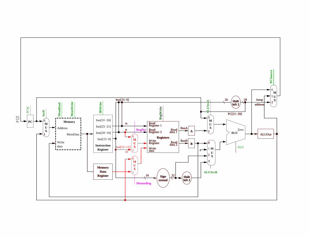
MUX
0
1
rd
Inst[15−11]
MUX
0
1
RegDst
MemtoReg
1
MemoryData
Register
1
MemoryData
Register
PC[31−28]
28
address
JumpInst[25−0] 262
1
0
2
Shiftleft 2
1
PC[31−28]
28
address
JumpInst[25−0] 262
1
1
0
2
Shiftleft 2
32
BusA
BusB
rs
rt
16
3
Registers
ReadRegister 2 A
B
Readdata 1
Register 1Read
data 2RegisterWrite
dataWrite
Read
extendSign Shift
left 2
ALUOut
Reg
Wri
te
32
BusA
BusB
rs
rt
16
3
Registers
ReadRegister 2 A
B
Readdata 1
Register 1Read
data 2RegisterWrite
dataWrite
Read
extendSign Shift
left 2
ALUOut
Reg
Wri
te
PC
ALUZero
4
0
Memory
Writedata
MemData
Address
MUX
0
1 M
XU
M
XU
MUX
0 Inst[31−26]
Inst[25−21]
Inst[15−0]
InstructionRegister
Inst[20−16]
PC
W
Mem
Wri
te
Mem
Rea
d
IorD IR
Wri
te
AL
USr
cA
ALUSrcB
ALU
PC
Sour
ce
254

Inst[5−0]
RegWrite
RegDstIRWrite
MemRead
PCWriteCond
PCWrite
IorD
MemWrite ALUSrcA
ALUSrcB
ALUOp
Control
Outputs
funct
op
ALUcontrol
MemtoReg
op
PCSource
MUX
0
1
MUX
0
1
rd
Inst[15−11]
MemtoReg
RegDst
1
MemoryData
Register
PC[31−28]
28
address
JumpInst[25−0] 262
1
1
0
2
Shiftleft 2
32
BusA
BusB
rs
rt
16
3
Registers
ReadRegister 2 A
B
Readdata 1
Register 1Read
data 2RegisterWrite
dataWrite
Read
extendSign Shift
left 2
ALUOut
Reg
Wri
te
PC
ALUZero
4
0
Memory
Writedata
MemData
Address
MUX
0
1 M
XU
M
XU
MUX
0 Inst[31−26]
Inst[25−21]
Inst[15−0]
InstructionRegister
Inst[20−16]
PC
W
Mem
Wri
te
Mem
Rea
d
IorD IR
Wri
te
AL
USr
cA
ALUSrcB
ALU
PC
Sour
ce
255

The control signals
The following control signals are identified in the datapath:
Action when
Signal 0 (deasserted) 1 (asserted)
RegDst the register written is the
rt field
the register written is the
rd field
RegWrite the register file will not be
written into
the register addressed by
the instruction will be
written into
ALUSrcA the first ALU operand is
the PC
the first ALU operand is
register A
MemRead no memory read occurs the contents of memory
at the specified address is
placed on the data bus
MemWrite no memory write occurs the contents of register B
is written to memory at
the specified address
MemtoReg the value written to the
register file comes from
ALUOut
the value written to the
register file comes from the
MDR
256

Action when
Signal 0 (deasserted) 1 (asserted)
IorD the memory address
comes from the PC (an
instruction)
the memory address
comes from ALUOut (a
data read)
IRWrite the IR is not written into the IR is written into (an
instruction is read)
PCWrite none (see below) the PC is written into;
the value comes from the
MUX controlled by the
signal PCSource
PCWriteCond if both it and PCWrite are
not asserted, the PC is not
written
the PC is written if the
ALU output Zero is active
257

Following are the 2-bit control signals:
Signal Value Action taken
ALUOp 00 ALU performs ADD operation
01 ALU performs SUBTRACT operation
10 ALU performs operation specified by funct
field
ALUSrcB 00 the second ALU operand is from register B
01 the second ALU operand is 4
10 the second ALU operand is the sign extended
low order 16 bits of the IR (imm16)
11 the second ALU operand is the sign extended
low order 16 bits of the IR shifted left by 2 bits
PCSource 00 the PC is updated with the value PC + 4
01 the PC is updated with the value in regis-
ter ALUOut (the branch target address, for a
branch instruction)
10 the PC is updated with the jump target address
The control unit must now be designed.
Since the instructions will now require several states, the control will
be a state machine, with the instruction op codes as inputs and the
control signals as outputs.
258

Review of instruction cycles and actions
Cycle Instruction type action
IF all IR ← Memory[PC]
PC ← PC + 4
ID all A ← Reg[rs]
B ← Reg[rt]
ALUOut ← PC + (imm16 <<2)
EX R-type ALUOut ← A op B
Load/Store ALUOut ← A + sign-extend(imm16)
Branch if (A == B) then PC ← ALUOut
Jump PC ← PC[31:28] || (IR[25:0] <<2)
MEM Load MDR ← Memory[ALUOut]
Store Memory[ALUOut] ← B
WB R-type Reg[rd] ← ALUOut
Load Reg[rt] ← MDR
Note that the first two steps are required for all instructions, and all
instructions require at least the first 3 cycles.
The MEM step is required only by the load and store instructions.
The ALU control unit is still a combinational logic block, as before.
259

Design of the control unit
The control unit is a state machine, implementing the state sequenc-
ing for every instruction.
Following is a partial state machine, detailing the IF and ID stages,
which are the same for all instructions:
IorD = 0ALUSrcA = 0Memread = 1
IRWrite = 1ALUSrcB = 01ALUOp = 00PCWrite = 1
PCSource = 00
0
ALUSrcB = 11ALUOp = 00
ALUSrcA = 0
1
Start
IF
ID
OP = ’BEQ’OP = ’R−type’OP = ’SW’OP = ’LW’ OP = ’J’
The partial state machines which implement each of the instructions
follow.
260

The combined control unit
MemtoReg = 0RegWrite = 1
RegDst = 1
7
IorD = 1MemRead = 1
3
IorD = 1MemWrite = 1
5
RegWrite = 1MemtoReg = 1
RegDst = 0
4
IorD = 0ALUSrcA = 0Memread = 1
IRWrite = 1ALUSrcB = 01ALUOp = 00PCWrite = 1
PCSource = 00
0
ALUSrcB = 11ALUOp = 00
ALUSrcA = 0
1
9
PCSource = 10PCWrite = 1ALUSrcB = 10
ALUOp = 00
ALUSrcA = 1
2
ALUSrcB = 00ALUOp = 10
ALUSrcA = 1
6
ALUSrcA = 1ALUSrcB = 00ALUOp = 01
PCWriteCond = 1
8
PCSource = 01OP = ’LW’
OP = ’SW’
Start
OP = ’J’OP = ’BEQ’OP = ’LW’
or
OP = ’SW’OP = ’R−type’
264
Implementing the control unit
All that remains is to implement the control unit is to design the
control logic itself.
Inputs are the instruction op codes, as before, and the outputs are
the control signals.
The following steps are typically followed in the implementation of
any sequential device:
• Construct the state diagram or equivalent (done).
• Assign numeric (binary) values to the states.
• Choose a memory element for state memory. (Normally, these
would be D flip flops or JK flip flops.)
• Design the combinational logic blocks to implement the next-
state functions.
• Design the combinational logic blocks to implement the outputs.
The actual implementation can be done in a number of ways; as
discrete logic, a PLA, read-only memory, etc.
Typically, the control unit would be automatically generated from a
description in some high level design language.
265

Adding exception handling
We will implement the hardware and control functions to handle two
types of exceptions; undefined instruction and arithmetic overflow.
Recall that the ALU had an overflow detection output, which can be
used as an input to the controller.
1. We will use a register labeled Cause to store a number (0 or 1)
to identify the type of exception, (0 for undefined instruction, 1
for arithmetic overflow).
It requires a control signal CauseWrite to be generated by the
controller. The controller also must set the value written to
the register, depending on whether or not the exception was an
arithmetic overflow.
The control signal IntCause is used to set this value.
2. The PC will be set to memory address C0000000 where the
operating system is expected to provide an event handler.
This is accomplished by adding another input (input 3) to the
MUX which updates the PC address. The MUX is controlled by
the 2-bit signal PCSource.
3. The address of the instruction which caused the exception is
stored in the register EPC, a 32 bit register.
Writing to this register is controlled by the new signal EPCWrite.
291

Storing the address of the instruction can be done several ways; for
example, it could be stored at the beginning of each instruction.
This would require a change to the datapath, and a way to disable
the storing of the address after each exception.
It is possible to store the address with only a small change to the
datapath (merely adding the EPC register to accept the output of the
ALU).
Recall that the next address (PC + 4) is calculated in the ALU, and
is written to the PC in the first cycle of every instruction. The ALU
can be used to subtract the value 4 from the PC after an exception
is detected, but before it is written into the EPC, so it contains the
actual address of the present instruction.
(Actually, there would be no real problem with saving the value
PC + 4 in the EPC; the interrupt handler could be responsible for
the subtraction.)
So, in order to handle these two exceptions, we have added two
registers — EPC and Cause, and three control signals — EPCWrite,
IntCause, and CauseWrite.
The changes to the processor datapath and control signals required
for the implementation of the exceptions detailed above are shown
in the following diagram.
292

ALUcontrol
RegWrite
RegDstIRWrite
MemRead
MemWrite ALUSrcA
ALUSrcB
op
Outputs
Control
EPCWrite
CauseWrite
PCSource
ALUOpIorD
PCWrite
PCWriteCond
MemtoReg
IntCause
PCMUX
0
1
Inst[31−26]
Inst[25−21]
Inst[20−16]
Inst[15−0]
InstructionRegister
MUX
0
1
MemoryData
RegisterextendSign Shift
left 2
dataWrite
RegisterWrite
ReadRegister 2
Register 1Read
Readdata 1
Readdata 2
Registers
B
A
M
XU
0
1
2
3
MUX
0
1
Shiftleft 2
M
XU
Memory
Writedata
MemData ALUZero
Inst[5−0]
32
BusA
BusB
4
Address
PC[31−28]
28
address
Jump
funct
rs
rt
MUX
0
1
Inst[25−0] 26
16
Inst[15−11]
rd
Cause
1
C0000000
2
1
0
3
MUX
0
1
0
overflowALUOut EPC
293

Adding exception handling to the control unit
The exceptions overflow and undefined can be implemented by
the addition of only one state each:
IntCause = 1CauseWrite = 1ALUSrcA = 0ALUSrcB = 01ALUOp = 01
PCSource = 11EPCWrite = 1PCWrite = 1
11
CauseWrite = 1ALUSrcA = 0ALUSrcB = 01ALUOp = 01
PCSource = 11EPCWrite = 1PCWrite = 1
IntCause = 0
10
overflow
OP = ’other’
to state 0
The input overflow is an output from the ALU. It is a combi-
national logic output, produced while the ALU is performing the
selected operation.
294

Thecontrolunit,
with
exceptio
nhandlin
g
IorD = 0ALUSrcA = 0Memread = 1
IRWrite = 1ALUSrcB = 01ALUOp = 00PCWrite = 1
PCSource = 00
0
ALUSrcB = 11ALUOp = 00
ALUSrcA = 0
1
9
PCSource = 10PCWrite = 1ALUSrcB = 00
ALUOp = 10
ALUSrcA = 1
6
ALUSrcB = 10ALUOp = 00
ALUSrcA = 1
2
IorD = 1MemRead = 1
3
IorD = 1MemWrite = 1
5
RegWrite = 1MemtoReg = 1
RegDst = 0
4
MemtoReg = 0RegWrite = 1
RegDst = 1
7IntCause = 1
CauseWrite = 1ALUSrcA = 0ALUSrcB = 01ALUOp = 01
PCSource = 11EPCWrite = 1PCWrite = 1
CauseWrite = 1ALUSrcA = 0ALUSrcB = 01ALUOp = 01
PCSource = 11EPCWrite = 1PCWrite = 1
IntCause = 0
ALUSrcA = 1ALUSrcB = 00ALUOp = 10
PCWriteCond = 1
8
PCSource = 01
Start
OP = ’J’OP = ’BEQ’OP = ’LW’
or
OP = ’SW’OP = ’R−type’
OP = ’LW’OP = ’SW’
OP = ’other’
11 10overflow overflow
TheALUoperation
which
could
resultin
anoverfl
owisdonein
the
EXcycle,
andtheoverflowsign
alisonlyavailab
lethen,unless
itis
savedin
aregister.
295
More about interrupts
The ability to handle interrupts and exceptions is an important fea-
ture for processors.
We have added the control logic to detect the two types of excep-
tions described earlier, but note that the Cause and the EPC register
cannot be read.
Instructions would have to be provided to allow these registers to be
read and manipulated.
Processors usually have policies relating to exceptions. The MIPS
processor had the policy that instructions which cause an exception
has no effect (e.g., nothing is written into a register.)
For some exceptions, if this policy is used, the operation may have
to complete before the exception can be detected, and the result of
the operation must then be “rolled back.”
This makes the implementation of exceptions difficult — sometimes
the state prior to an operation must be saved so it can be restored.
This constraint alone sometimes results in instructions requiring more
cycles for their implementation.
299

Exceptions and interrupts in other processors
A common type of interrupt is a vectored interrupt. Here, differ-
ent interrupts or exceptions jump to different addresses in memory.
The operating system places an appropriate interrupt handler for the
particular interrupt at each of these locations.
A vectored interrupt both identifies the type of interrupt, and pro-
vides the handler at the same time. (Since different interrupts or
exceptions have different vectors.)
In the INTEL processors, it is the responsibility of the interrupting
device to provide the interrupt vector. (This is usually done by
one of the peripheral controller chips, under control of the operating
system.)
A major problem with the PC architecture is that only a small num-
ber of interrupts (typically 16) can be handled by the controller chip.
this has lead to many problems with hardware devices “sharing in-
terrupts” — defeating the advantages of vectored interrupts.
We will look at interrupts again, later, when we discuss input and
output devices.
300

Some questions about exceptions and interrupts
The following questions often have different answers for different pro-
cessors:
• How does a processor return control of the program flow from
the exception or interrupt handler to the interrupted program?
Some processors have explicit instructions for this (e.g., the MIPS
processors), others treat interrupts and exceptions as being sim-
ilar to subprogram calls (INTEL processors do this.)
• What happens when an exception or interrupt is itself inter-
rupted?
Some processors save the return addresses in a stack data struc-
ture, and successive levels of interrupts just increase the stack
depth. Typically, this is the way subprogram return addresses
are also stored.
Some processors automatically turn off the interrupt capability
at the beginning of an interrupt, and it must be explicitly turned
back on by the interrupt or exception handler to accept another
interrupt.
Some processors have both features — instructions can turn the
interrupt capability on and off, and can allow interrupts to be
interrupted themselves. (This turns out to be important for
implementing certain operating system functions.)
301

Comments on our implementation of exceptions
Note that our implementation has only one register for the address
of the interrupting instruction, and no way to read that address and
modify it to resume the program where the exception occurred.
What changes would be required to the instruction set accomplish
this?
The simplest solution would probably be to allow only one interrupt
at a time, by disabling the interrupt capability, and to provide:
1. An instruction to store the EPC in the register file.
2. An instruction to store the Cause register in the register file.
3. An instruction to turn on interrupt capability after the next
instruction completed execution. (This assumes that the next
instruction restores the PC to the address of the instruction fol-
lowing the one that caused the exception.)
Note that these would require changes to the datapath and control.
This example was just to give the flavor of the problems involved
with handling exceptions in the processor. More complex instruction
sets and architectures exacerbate the problems.
302

Comments on handling interrupts
Although exception handling is complex, it is often simpler than the
handling of external interrupts.
Exceptions occur as a result of occurrences internal to the processor.
Consequently, they are usually both predictable, and occur and are
detected at known times in the execution of a particular instruction.
Interrupts are external events, and are not at all synchronized with
the execution of instructions in the processor.
Since interrupts may be notification of an urgent event, they usually
require fast servicing.
Decisions therefore have to be taken about exactly when in the exe-
cution of an instruction an interrupt will be detected and handled.
Some of the considerations are:
• If the instruction is not allowed to complete, information must
be retained in order to either continue or restart the interrupted
instruction. How will this be done?
• If the interrupted instruction is allowed to complete, how will the
processor return to the next instruction in the current program?
• Can the interrupt handler be interrupted?
• Can interrupts be prioritized so that a high priority interrupt
can interrupt a lower priority interrupt?
303