
2nd-Order Neural Core for Bioinspired Focal-Plane Dynamic …petras/cikkek/tnn.pdf · The visual...
20
2nd-Order Neural Core for Bioinspired Focal-Plane Dynamic Image Processing in CMOS Ricardo Carmona 1 , Francisco Jiménez-Garrido 1 , Carlos M. Domínguez-Mata 1 , Rafael Domínguez-Castro 1 , Servando Espejo 1 , Istvan Petras 2 and Ángel Rodríguez-Vázquez 1 1 Instituto de Microelectrónica de Sevilla-CNM-CSIC Campus de la Universidad de Sevilla. Avda. Reina Mercedes s/n, Edificio CICA 41012-Sevilla, Spain. Tel.: +34955056666, Fax: +34955056686 E-mail: [email protected] 2 Analogic and Neural Computing Laboratory Hungarian Academy of Sciences ABSTRACT Based on studies of the mammalian retina, a bioinspired model for mixed-signal array processing has been implemented on silicon. This model mimics the way in which images are processed at the front-end of natural visual pathways, by means of programmable complex spatio-temporal dynamic. When embedded into a focal- plane processing chip, such model allows for on-line parallel filtering of the cap- tured image; the outcome of such processing can be used to develop control feed- back actions to adapt the response of photoreceptors to local image features. Beyond simple resistive grid filtering, it is possible to program other spatio-temporal processing operators into the model core, such as nonlinear and anisotropic diffu- sion, among others. This paper presents analog and mixed-signal VLSI building blocks to implement this model, and illustrates their operation through experimental results taken from a prototype chip fabricated in a CMOS technology. I. INTRODUCTION Physiological and pharmacological studies of the mammalian retina show that this amazing piece of wetware is not a simple phototransducer, but is responsible for very complex signal processing. The retina operates on the captured visual stimuli at early stages in the process of vision. Complex spatio-temporal processing encodes visual information into a reduced set of channels [1]. The visual information flow is compressed into a data set of a manageable size, to be delivered to the brain by the optic nerve. Although the mapping is retinotopic, it is not the raw image brightness that is sent to the visual cortex, but a specific set of image features (closely related with the spatial and temporal characteristics of the visual stimulus) which are obtained and codified in the retina. The purpose of this early vision processing is to alleviate the work of the central nervous system. The application of a highly regular computational task onto a large set of simple data (e.g. picture brightness samples) is transferred to the retina, while the cortex 0.5 μ m
-
Upload
duongtuyen -
Category
Documents
-
view
213 -
download
0
Transcript of 2nd-Order Neural Core for Bioinspired Focal-Plane Dynamic …petras/cikkek/tnn.pdf · The visual...
2nd-Order Neural Core for Bioinspired Focal-Plane Dynamic Image Processing in CMOS
Ricardo Carmona 1, Francisco Jiménez-Garrido 1, Carlos M. Domínguez-Mata 1, Rafael Domínguez-Castro 1, Servando Espejo 1, Istvan Petras 2 and Ángel Rodríguez-Vázquez 1
1 Instituto de Microelectrónica de Sevilla-CNM-CSICCampus de la Universidad de Sevilla. Avda. Reina Mercedes s/n, Edificio CICA
41012-Sevilla, Spain. Tel.: +34955056666, Fax: +34955056686E-mail: [email protected]
2 Analogic and Neural Computing LaboratoryHungarian Academy of Sciences
ABSTRACT
Based on studies of the mammalian retina, a bioinspired model for mixed-signalarray processing has been implemented on silicon. This model mimics the way inwhich images are processed at the front-end of natural visual pathways, by meansof programmable complex spatio-temporal dynamic. When embedded into a focal-plane processing chip, such model allows for on-line parallel filtering of the cap-tured image; the outcome of such processing can be used to develop control feed-back actions to adapt the response of photoreceptors to local image features. Beyondsimple resistive grid filtering, it is possible to program other spatio-temporalprocessing operators into the model core, such as nonlinear and anisotropic diffu-sion, among others. This paper presents analog and mixed-signal VLSI buildingblocks to implement this model, and illustrates their operation through experimentalresults taken from a prototype chip fabricated in a CMOS technology.
I. INTRODUCTION
Physiological and pharmacological studies of the mammalian retina show that this amazingpiece of wetware is not a simple phototransducer, but is responsible for very complex signalprocessing. The retina operates on the captured visual stimuli at early stages in the process ofvision. Complex spatio-temporal processing encodes visual information into a reduced set ofchannels [1]. The visual information flow is compressed into a data set of a manageable size, tobe delivered to the brain by the optic nerve. Although the mapping is retinotopic, it is not theraw image brightness that is sent to the visual cortex, but a specific set of image features (closelyrelated with the spatial and temporal characteristics of the visual stimulus) which are obtainedand codified in the retina. The purpose of this early vision processing is to alleviate the work ofthe central nervous system. The application of a highly regular computational task onto a largeset of simple data (e.g. picture brightness samples) is transferred to the retina, while the cortex
0.5µm
2nd-Order Neural Core for Bioinspired Focal-Plane Dynamic Image Processing in CMOS 2
activity is dedicated to higher level operations on more complex data structures. The massiveparallelism of this model inspires a feasible alternative to conventional digital image processing.The limited bandwidth available for transferring signals between the camera array and the proc-essor, and the limited computing speed achievable in a serial, or timidly parallel, processingarchitecture, make these systems fail to match the tight requirements found in real-time imageprocessing.
We are interested in local monitoring and control of the photosensing devices for contrastenhancement. This capability improves the perceived sensation by extracting the reflectanceinformation from the acquired luminance matrix [2]. Data bottlenecks, arising mostly in trans-ferring image samples from the camera to the processor, and in delivering the appropriate con-trol signals to each photosensor, and the enormous amount of data to be processed, make ithardly realizable at a practical frame rate by a conventional digital processing system. Yet, thistask is gracefully implemented in the biological retina. Concurrent processing and sensing elim-inate data bottlenecks in the forward and feedback paths, and massively parallel processing pro-vides enough computing power. Mixed-signal VLSI permits the implementation of massivelyparallel multidimensional signal processing without serious area and power penalties. Thesechips are called neuromorphic [3] as they mimic the way in which the layers of neurons in thebiological retina realize early vision.
An image acquisition and focal-plane processor chip must have, at every pixel, a reliable,locally adaptive photosensing device (the opto-electronic interface) plus the analog and/ormixed-signal core which realizes signal processing at the pixel-level. Concerning the distributedprocessing facilities, the CNN universal machine architecture [4] has several advantages. It hasan analog front-end, which is compatible with the nature of the signals coming from the photo-sensors, it is general-purpose and fully programmable, it has a distributed memory to store inter-mediate results, and it has been proven to realize the type of processing required for sensorcontrol [5]. In addition, retinal features have been successfully modelled and simulated withinthe CNN framework [6].
This paper presents, in the first place, a network model inspired on the layered structure of themammalian retina. Then the implementation of a fully-programmable 2nd-order neural core toprovide active wave computing at the focal-plane is shown. By setting the appropriate parame-ters: such as interaction strengths, time constants and bias terms, an array of such processing ele-ments can emulate some phenomena observed in the mammalian retina. At the end of the paper,experiments in a CMOS prototype of cells, each one containing a 2nd-orderneural core, are displayed.
II. BIOINSPIRED NETWORK MODEL
A) A sketch of the mammalian retina
The retina is a peripheral component of the central nervous system responsible of acquiringand coding the information contained in the visual stimuli. Specialized neurons develop a par-ticular kind of massively parallel processing of raw sensory information. Visual stimuli triggerpatterns of activation in the layered structure of the retina, which are processed as they advance
0.5µm 32 32×
2nd-Order Neural Core for Bioinspired Focal-Plane Dynamic Image Processing in CMOS 3
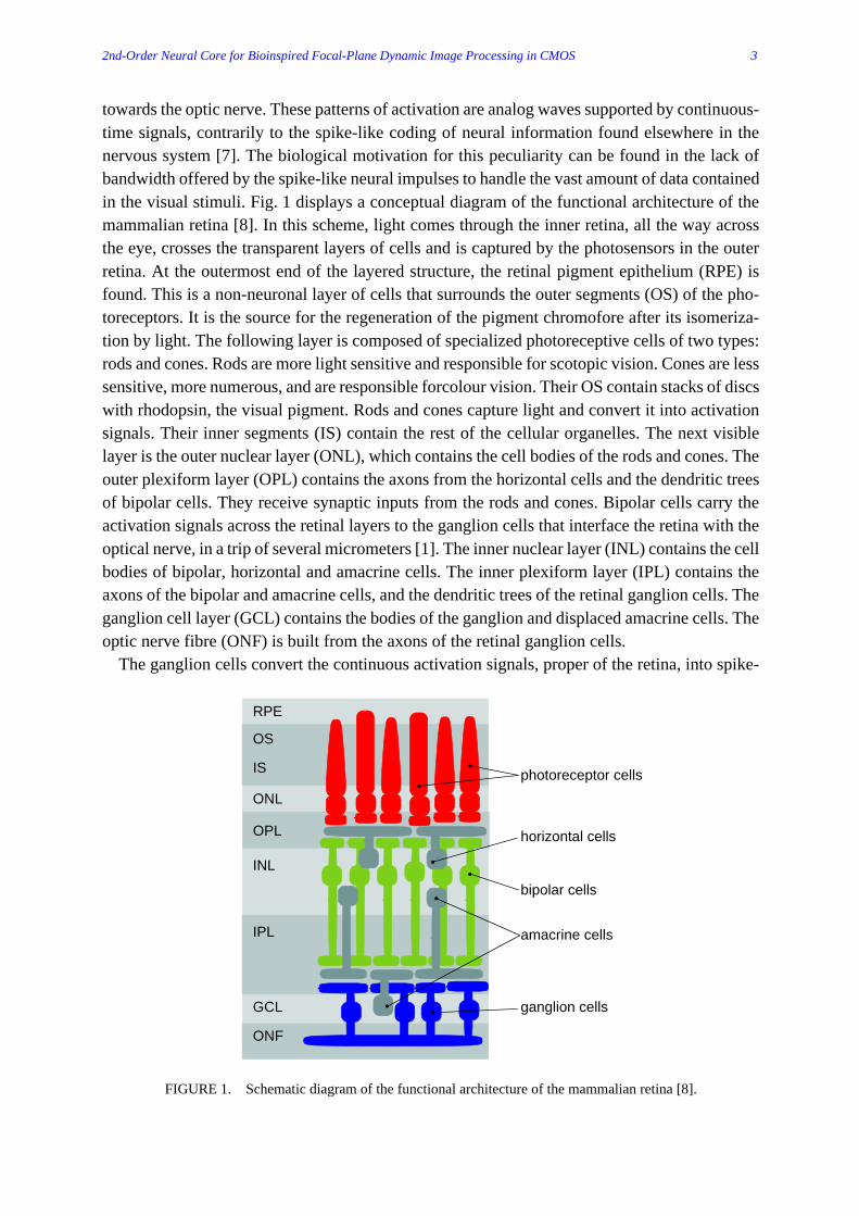
towards the optic nerve. These patterns of activation are analog waves supported by continuous-time signals, contrarily to the spike-like coding of neural information found elsewhere in thenervous system [7]. The biological motivation for this peculiarity can be found in the lack ofbandwidth offered by the spike-like neural impulses to handle the vast amount of data containedin the visual stimuli. Fig. 1 displays a conceptual diagram of the functional architecture of themammalian retina [8]. In this scheme, light comes through the inner retina, all the way acrossthe eye, crosses the transparent layers of cells and is captured by the photosensors in the outerretina. At the outermost end of the layered structure, the retinal pigment epithelium (RPE) isfound. This is a non-neuronal layer of cells that surrounds the outer segments (OS) of the pho-toreceptors. It is the source for the regeneration of the pigment chromofore after its isomeriza-tion by light. The following layer is composed of specialized photoreceptive cells of two types:rods and cones. Rods are more light sensitive and responsible for scotopic vision. Cones are lesssensitive, more numerous, and are responsible forcolour vision. Their OS contain stacks of discswith rhodopsin, the visual pigment. Rods and cones capture light and convert it into activationsignals. Their inner segments (IS) contain the rest of the cellular organelles. The next visiblelayer is the outer nuclear layer (ONL), which contains the cell bodies of the rods and cones. Theouter plexiform layer (OPL) contains the axons from the horizontal cells and the dendritic treesof bipolar cells. They receive synaptic inputs from the rods and cones. Bipolar cells carry theactivation signals across the retinal layers to the ganglion cells that interface the retina with theoptical nerve, in a trip of several micrometers [1]. The inner nuclear layer (INL) contains the cellbodies of bipolar, horizontal and amacrine cells. The inner plexiform layer (IPL) contains theaxons of the bipolar and amacrine cells, and the dendritic trees of the retinal ganglion cells. Theganglion cell layer (GCL) contains the bodies of the ganglion and displaced amacrine cells. Theoptic nerve fibre (ONF) is built from the axons of the retinal ganglion cells.
The ganglion cells convert the continuous activation signals, proper of the retina, into spike-
FIGURE 1. Schematic diagram of the functional architecture of the mammalian retina [8].
RPE
OS
IS
ONL
OPL
INL
IPL
GCL
ONF
photoreceptor cells
horizontal cells
bipolar cells
amacrine cells
ganglion cells
2nd-Order Neural Core for Bioinspired Focal-Plane Dynamic Image Processing in CMOS 4
coded signals which can be transmitted over longer distances by the nervous system. On its wayto the ganglion cells, the information carried by bipolar cells is affected by the operation of thehorizontal and amacrine cells. They form layers in which activation signals are weighted andpromediated in order to, first, bias photodetectors and, second, to account for inhibition on thevertical pathway. The four main transformations that take place in this structure are: the pho-toreceptor gain control, the gain control of the bipolar cells, the generation of transient activityand the transmission of transient inhibition [1]. Briefly, captured stimuli are promediated andthe high-gain characteristics of the cones and the bipolar cells are shifted to adapt to the partic-ular light conditions. These operations have a local scope and depend on the recent history ofthe cells. Once adaptation is achieved, patterns of activity are formed dynamically by the pres-ence or absence of visual stimuli. Also inhibition is generated and transmitted laterally throughthe layers of horizontal and amacrine cells. As a result of these transformations, the patterns ofactivity reach the layer of ganglion cells. At this point, the patterns are converted into pulse-coded signals that are sent to the brain to be interpreted. In a sense, the layered structure of theretina translates the visual stimuli into a compressed language which can be understood by thebrain in recreating vision.
B) CNN analogy of the inner and outer plexiform layers
In the above description there are some aspects of the retinal layers that markedly resemblethe features of a cellular neural network (CNN) [9]: the 2D aggregation of continuous signals,the local connectivity between elementary nonlinear processors, and the analog weighted inter-actions between them. Also, the complete signal pathway in the retina has the topology of a 3Dnetwork, or, more properly network, a pile of 2D layers connected vertically. Motivatedby these coincidences, a CNN model has been developed which approximates the observedbehaviour of different parts of the mammalian retina. For instance, the outer plexiform layer(OPL). The OPL is responsible for the generation of the first activation patterns immediatelyafter image capture. It has been characterized by experimental measurements, leading to amodel with three different layers [10]. These layers stand for the contribution of photoreceptors,horizontal and bipolar cells. Each of them has the structure of a 2D CNN itself. Each of themhas its own interaction patterns (CNN templates) and its particular time constant. Cell dynamicsat each layer are supported by a first or a second order continuous-time core.
The inner plexiform layer (IPL) has been also modelled within the CNN framework. The IPLis responsible for the generation of the retinal output. A simplified model of the IPL has threelayers. Two of them represent the influence of the wide field amacrine cells excited by the inputsignal, which in this case is the output of the bipolar cells, and there is a third layer that controlsthe dynamic of the previous layers by means of feedback. As before, the three layers can be seenas 2D CNNs with their own internal coupling and their own time constant [10].
Because of the relative simplicity of these models, a programmable CNN chip has been pro-posed [11]. The programmable array processor consists of 2 coupled CNN layers. Each elemen-tary processor contains the nodes for both CNN layers. The third layer, supporting analogarithmetics, is implemented off-line by these analog cores, with the help of the local facilitiesfor analog signal storage. The evolution of the coupled CNN nodes of a specific cell isdescribed by these coupled differential equations:
212---D
C i j,( )
2nd-Order Neural Core for Bioinspired Focal-Plane Dynamic Image Processing in CMOS 5
(1)
where the loss term and the activation function are those of the FSR CNN model [12]:
(2)
and:
(3)
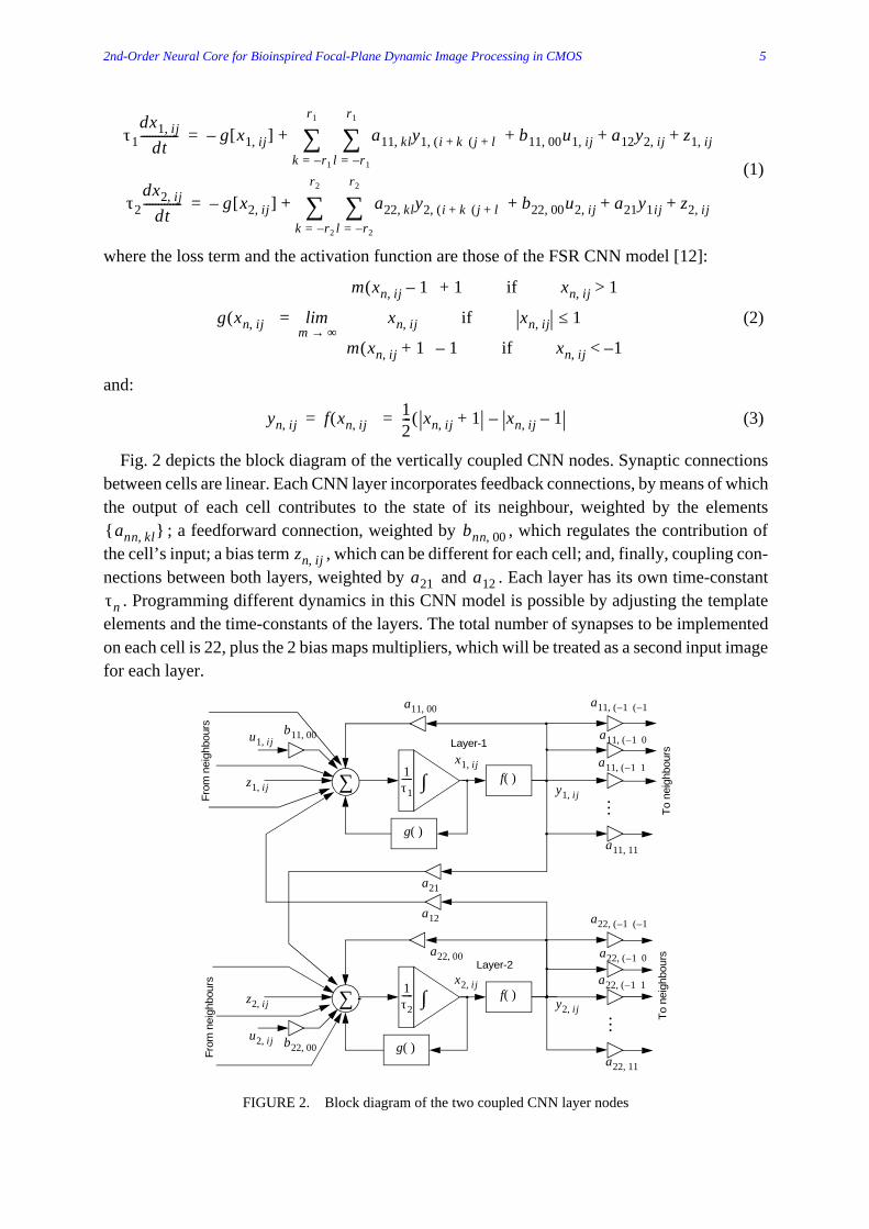
Fig. 2 depicts the block diagram of the vertically coupled CNN nodes. Synaptic connectionsbetween cells are linear. Each CNN layer incorporates feedback connections, by means of whichthe output of each cell contributes to the state of its neighbour, weighted by the elements
; a feedforward connection, weighted by , which regulates the contribution ofthe cell’s input; a bias term , which can be different for each cell; and, finally, coupling con-nections between both layers, weighted by and . Each layer has its own time-constant
. Programming different dynamics in this CNN model is possible by adjusting the templateelements and the time-constants of the layers. The total number of synapses to be implementedon each cell is 22, plus the 2 bias maps multipliers, which will be treated as a second input imagefor each layer.
τ1dx1 ij,
dt------------- g x1 ij,[ ]– a11 kl,
l r– 1=
r1
∑ y1 i k+( ) j l+( ), b11 00, u1 ij, a12y2 ij, z1 ij,+ + +k r– 1=
r1
∑ +=
τ2dx2 ij,
dt------------- g x2 ij,[ ]– a22 kl,
l r– 2=
r2
∑ y2 i k+( ) j l+( ), b22 00, u2 ij, a21y1ij z2 ij,+ + +k r– 2=
r2
∑ +=
g xn ij,( )
m xn ij, 1–( ) 1+ if xn ij, 1>
xn ij, if xn ij, 1≤
m xn ij, 1+( ) 1– if xn ij, 1–<
m ∞→lim=
yn ij, f xn ij,( ) 12--- xn ij, 1+ xn ij, 1––( )= =
FIGURE 2. Block diagram of the two coupled CNN layer nodes
1τ2----- ∫
g ( )
f ( ) ∑ y2 i j,z2 i j,
u2 i j,
a22 00,
b22 00,
a22 1–( ) 1–( ),
a22 1–( )0,
a22 1–( )1,
a22 11,
…
a12
1τ1----- ∫
g ( )
f ( ) ∑ y1 i j,z1 i j,
u1 i j,
a11 00,
b11 00,
a11 1–( ) 1–( ),
a11 1–( )0,
a11 1–( )1,
a11 11,
…
a21
x2 i j,
x1 ij,
To
neig
hbou
rsT
o ne
ighb
ours
Fro
m n
eigh
bour
s
Layer-1
Fro
m n
eigh
bour
s
Layer-2
ann kl,{ } bnn 00,zn ij,
a21 a12τn
2nd-Order Neural Core for Bioinspired Focal-Plane Dynamic Image Processing in CMOS 6
III. 2ND-ORDER CORE IMPLEMENTATION
A) 2nd-order cell structure
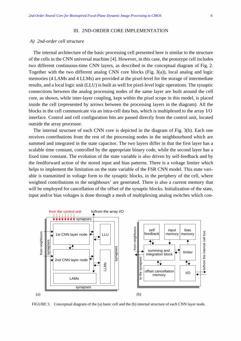
The internal architecture of the basic processing cell presented here is similar to the structureof the cells in the CNN universal machine [4]. However, in this case, the prototype cell includestwo different continuous-time CNN layers, as described in the conceptual diagram of Fig. 2.Together with the two different analog CNN core blocks (Fig. 3(a)), local analog and logicmemories (4 LAMs and 4 LLMs) are provided at the pixel-level for the storage of intermediateresults, and a local logic unit (LLU) is built as well for pixel-level logic operations. The synapticconnections between the analog processing nodes of the same layer are built around the cellcore, as shown, while inter-layer coupling, kept within the pixel scope in this model, is placedinside the cell (represented by arrows between the processing layers in the diagram). All theblocks in the cell communicate via an intra-cell data bus, which is multiplexed to the array interface. Control and cell configuration bits are passed directly from the control unit, locatedoutside the array processor.
The internal structure of each CNN core is depicted in the diagram of Fig. 3(b). Each onereceives contributions from the rest of the processing nodes in the neighbourhood which aresummed and integrated in the state capacitor. The two layers differ in that the first layer has ascalable time constant, controlled by the appropriate binary code, while the second layer has afixed time constant. The evolution of the state variable is also driven by self-feedback and bythe feedforward action of the stored input and bias patterns. There is a voltage limiter whichhelps to implement the limitation on the state variable of the FSR CNN model. This state vari-able is transmitted in voltage form to the synaptic blocks, in the periphery of the cell, whereweighted contributions to the neighbours’ are generated. There is also a current memory thatwill be employed for cancellation of the offset of the synaptic blocks. Initialization of the state,input and/or bias voltages is done through a mesh of multiplexing analog switches which con-
FIGURE 3. Conceptual diagram of the (a) basic cell and the (b) internal structure of each CNN layer node.
limiter
offset cancellationmemory I/O
selffeedback
inputmemory
biasmemory
to th
e sy
naps
es
summing and integration block
to/fr
om th
e in
tern
al c
ell b
us
(a) (b)
from
nei
ghbo
urs
LAMs
synapses
synapses
LLM
s
LLU
2nd CNN layer node
1st CNN layer node
from
nei
ghbo
urs
syna
pses
syna
pses
to/from the array I/Ofrom the control unit
I/O
2nd-Order Neural Core for Bioinspired Focal-Plane Dynamic Image Processing in CMOS 7
nect to the cell’s internal data bus.Running complex spatio-temporal dynamics in this network requires following several ini-
tialization and calibration steps. First of all, acquisition of the input image and auxiliary masksand/or patterns. To this purpose, the array interface is directed to specific LAM locationsin a row-by-row basis. After that, the analog instruction, i. e. the set of synaptic weights requiredfor a specific operation, is selected and transmitted to all the cells in the array. Then, the offsetof the critical OPAMPs is extracted in a calibration step. After that, the time-invariant offsets ofthe synaptic blocks are computed and stored in the current memories. Now the network is almostready to operate. The state capacitors and the feedforward synapses are then initialized by meansof the appropriate switch configuration, and the network evolution is run by closing the feed-back loop in each processing element. Before stopping the network evolution, the final state isstored in a LAM register for further operation.
B) Single-transistor synapse
One of the most important blocks in the cell is the synaptic block. The synapse is, simply, afour-quadrant analog multiplier. Its inputs are the cell state, , or input, , variables and thecorresponding weight signal, , while the output is the cell’s contribution to a specific neigh-bouring cell. The multiplier is required to have voltage inputs, which can be easily conveyed toany high-impedance node by a simple wire, and current output, which may be easily summedby wiring all current contributions concurrently to a low-impedance node. Two important factsfor the implementation of the synaptic blocks are, first, that there is no need to have a strictlylinear relation between the weight signal, , and the output current, , and second, that theweight signal does not change during the evolution of the network. Thus, any deviation depend-ing on is not a gain error, but an offset error, i.e. an error which can be cancelled by auto-zeroing in a pre-processing calibration step.
Direct multiplication can be achieved by a MOS transistor operating in the ohmic region. Itslow-frequency large-signal characteristic is found in the first-order approach by (if n-type):
(4)
where . A multiplication can be realized with this device as long as holds [13]. This alternative has several advantages, compared with
multipliers built with MOS transistors in weak inversion or in strong inversion saturation [14]:it requires a reduced amount of area, because four-quadrant behaviour is achieved with one sin-gle transistor. In addition, it has a better relation between bias power and signal power, thus lead-ing to higher accuracy at lower power consumption, while in the saturation region theinformation is carried by a small fraction of the actual currents flowing through the devices.Third, the use of the ohmic region shows better mismatch figures than any other region [15].
The one-transistor synapse works as follows. Consider a p-type MOS transistor operating inthe ohmic region (Fig. 4). The transistor selected is of type p because the more resistive p-typechannel requires smaller currents (hence smaller power consumption) for the same transistorlengths. Alternatively, for the same current levels, the required p-channel MOS is shorter thanits n-type counterpart. The source-to-drain current of a PMOS transistor in the ohmic region is
I/O
Vx VuVw
Vw Io
Vw
IDS βn VGS VT VSB( )–VDS
2---------– VDS=
βn µoCox' W L⁄( )=VDS 2 VGS VT VSB( )–[ ]«

2nd-Order Neural Core for Bioinspired Focal-Plane Dynamic Image Processing in CMOS 8
given by:
(5)
where the threshold adopts one of these two analogue forms:
(6)
must be kept fixed in order to use and as single-ended input voltages, and to sense as the output of the synapse. For this purpose we can employ a current conveyor [16] at the
current input node of each cell. The current conveyor permits current sensing while maintaininga virtual reference at node . All the synapses contributing to the same cell can be connectedto the same virtual reference. The only objection is that the impedance at this node must be wellbelow the parallel of the output impedances of all the synaptic blocks.
Back to Eq. (5), notice that the second term on the right side of the equation does not dependon , therefore node is a strong candidate to hold the cell state variable voltage. But must always be positive for the MOS transistor to operate above threshold, thus let be com-posed of a reference voltage , sufficiently high, and a superposed cell state signal :
(7)
And, in order to achieve four-quadrant multiplication, must be permitted to go above andbelow . Let us select as the reference for the weight signal, , being:
(8)
Eq. (5) can then be rewritten as:
(9)
which is a four-quadrant multiplier with an offset term which is time-invariant (at least duringthe transient evolution of the network) and does not depend on the cell state. Therefore, we havearrived at a four-quadrant multiplier with single-ended voltage inputs and a current output, witha offset which can be eliminated by a calibration step, with the help of a current memory:
(10)
FIGURE 4. Multiplier using one single MOS transistor in the ohmic region.
VA VL
Io
VB
AL
BVG
G
Io β– p VA VL–( )VG βp VA VL–( ) V̂Tp
VA VL+2
-------------------– –=
V̂Tp
VT0p– γ φB VDD VA–+ φB–( )– if VA VL≥
VT0p– γ φB VDD VL–+ φB–( )– if VA VL≤
=
VL VA VGIo
L
VG G VGVG
Vx0Vx
VG VX≡ Vx0Vx+=
VAVL VL Vw0
VA VW≡ Vw0Vw+=
Io β– pVwVx βpVw Vx0V̂Tp
Vw0–
Vw
2------–+
–=
Io β– pVwVx Ioffset Vw( )+=
2nd-Order Neural Core for Bioinspired Focal-Plane Dynamic Image Processing in CMOS 9
The limitations found to this behaviour are the upper and lower boundaries of the ohmicregion in strong inversion and the degradation of the mobility. The transversal electric fieldpushes the carriers towards the semiconductor surface where they suffer scattering, whichrenders a reduction in the speed of the carriers, thus degrading the mobility. This transversalelectric field depends on the gate voltage, thus the first summand in Eq. (10) is no longer linearwith . Combining the two limiting factors:
(11)
where is a maximum effective gate voltage, beyond whichthe distortion introduced by mobility degradation exceeds the linearity requirements.
For moderate linearity requirements, in a typical CMOS technology, the right hand side ofEq. (11) becomes approximately equal to 1V. If and are assigned the same voltage
ranges, around their reference values, then . With these
values of , and , must be kept 1.6V below . Thus, must be
high enough to leave room for , but not too large because the weight signal will progress up
to above . In addition, we have to provide a range for the current conveyor circuitry
to maintain a virtual reference precisely at , and for the circuits generating the weight volt-
ages, which will have a limited output swing. If we select , then they are
above before hitting the power rail at , which means one , approximately. With
this value, results in . Finally, once the voltage ranges are fixed, a maximum current
per synapse is selected for meeting power requirements, in this case it will be . With these
values, the synapse is dimensioned. In this chip, it will be wide and long.
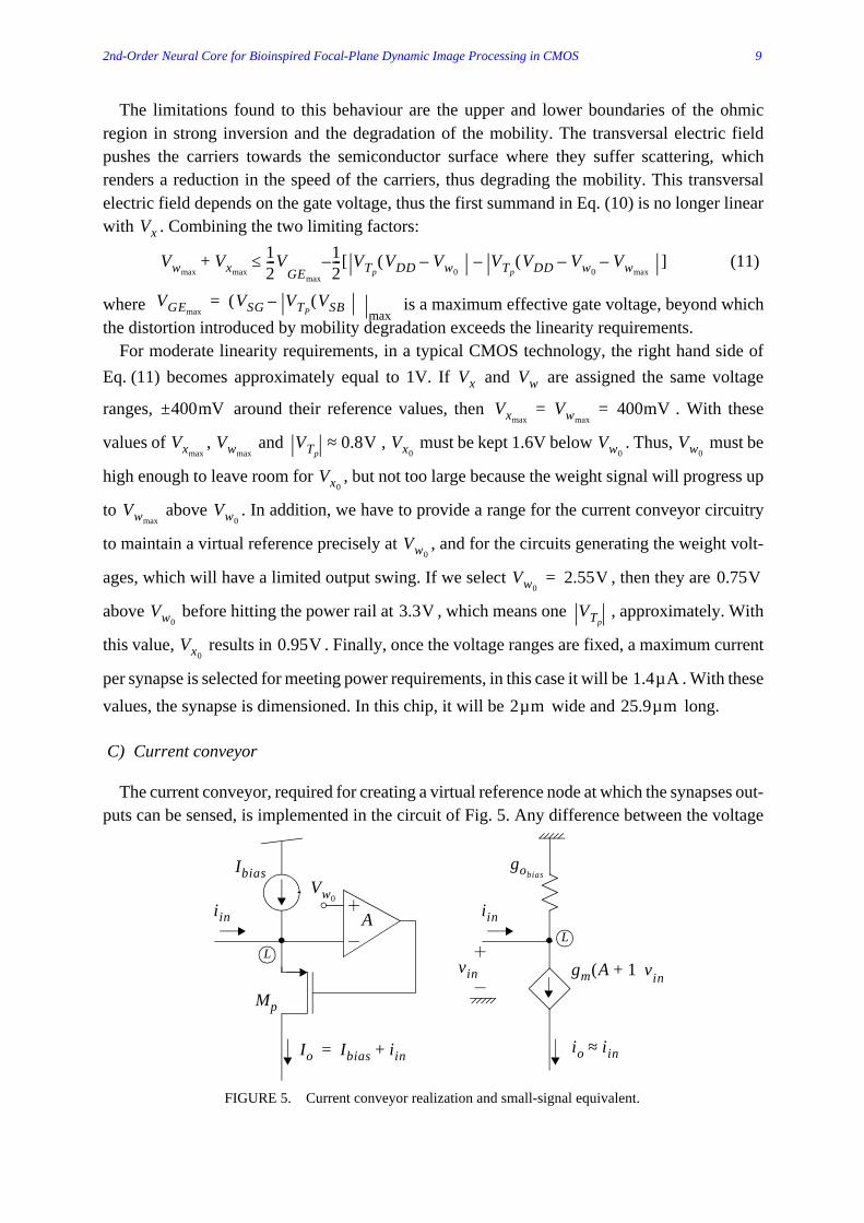
C) Current conveyor
The current conveyor, required for creating a virtual reference node at which the synapses out-puts can be sensed, is implemented in the circuit of Fig. 5. Any difference between the voltage
Vx
VwmaxVxmax
+ 12---V
GEmax
12--- VTp
VDD Vw0–( ) VTp
VDD Vw0– Vwmax
–( )–[ ]–≤
VGEmaxVSG VTP
VSB( )–( )max
=
Vx Vw
400± mV VxmaxVwmax
400mV= =
VxmaxVwmax
VTp0.8V≈ Vx0
Vw0Vw0
Vx0
VwmaxVw0
Vw0
Vw02.55V= 0.75V
Vw03.3V VTp
Vx00.95V
1.4µA
2µm 25.9µm
FIGURE 5. Current conveyor realization and small-signal equivalent.
iin
Ibias
Io Ibias iin+=
Vw0
iin
gobias
io iin≈
vin gm A 1+( )vin
A
LL
Mp
2nd-Order Neural Core for Bioinspired Focal-Plane Dynamic Image Processing in CMOS 10
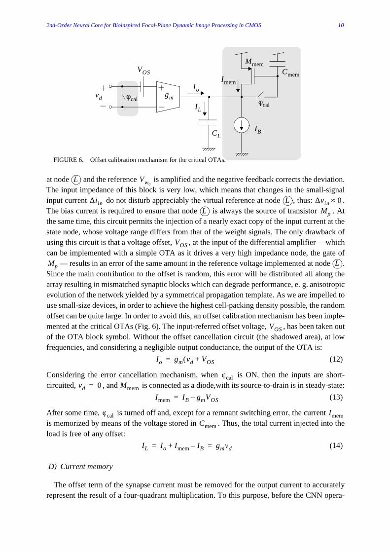
at node and the reference is amplified and the negative feedback corrects the deviation.The input impedance of this block is very low, which means that changes in the small-signalinput current do not disturb appreciably the virtual reference at node , thus: .The bias current is required to ensure that node is always the source of transistor . Atthe same time, this circuit permits the injection of a nearly exact copy of the input current at thestate node, whose voltage range differs from that of the weight signals. The only drawback ofusing this circuit is that a voltage offset, , at the input of the differential amplifier —whichcan be implemented with a simple OTA as it drives a very high impedance node, the gate of
— results in an error of the same amount in the reference voltage implemented at node .Since the main contribution to the offset is random, this error will be distributed all along thearray resulting in mismatched synaptic blocks which can degrade performance, e. g. anisotropicevolution of the network yielded by a symmetrical propagation template. As we are impelled touse small-size devices, in order to achieve the highest cell-packing density possible, the randomoffset can be quite large. In order to avoid this, an offset calibration mechanism has been imple-mented at the critical OTAs (Fig. 6). The input-referred offset voltage, , has been taken outof the OTA block symbol. Without the offset cancellation circuit (the shadowed area), at lowfrequencies, and considering a negligible output conductance, the output of the OTA is:
(12)
Considering the error cancellation mechanism, when is ON, then the inputs are short-circuited, , and is connected as a diode,with its source-to-drain is in steady-state:
(13)
After some time, is turned off and, except for a remnant switching error, the current is memorized by means of the voltage stored in . Thus, the total current injected into theload is free of any offset:
(14)
D) Current memory
The offset term of the synapse current must be removed for the output current to accuratelyrepresent the result of a four-quadrant multiplication. To this purpose, before the CNN opera-
L Vw0
∆iin L ∆vin 0≈L Mp
VOS
Mp L
FIGURE 6. Offset calibration mechanism for the critical OTAs.
CL
gm
IB
Imem
φcal
MmemCmem
vd
VOS
φcalIL
Io
VOS
Io gm vd VOS+( )=
φcalvd 0= Mmem
Imem IB gmVOS–=
φcal ImemCmem
IL Io Imem IB–+ gmvd= =
2nd-Order Neural Core for Bioinspired Focal-Plane Dynamic Image Processing in CMOS 11
tion, but right after the new weights have been up-loaded, all the synapses are reset to. The resulting current, which is the sum of the offset currents of all the synapses con-
currently connected to the same node, is memorized. This value will be subtracted on-line fromthe input current during the network evolution, resulting in a one-step cancellation of the errorsof all the synapses. The validity of this method relies on the accuracy of the current memory.For instance, in this chip, the sum of all the contributions will range from to . Onthe other hand, the maximum current signal of the synapse is:
(15)
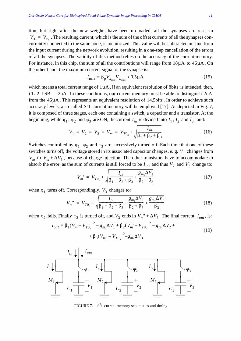
which means a total current range of . If an equivalent resolution of is intended, then,. In these conditions, our current memory must be able to distinguish
from the . This represents an equivalent resolution of . In order to achieve suchaccuracy levels, a so-called current memory will be employed [17]. As depicted in Fig. 7,it is composed of three stages, each one containing a switch, a capacitor and a transistor. At thebeginning, while , and are ON, the current is divided into , and , and:
(16)
Switches controlled by , and are successively turned off. Each time that one of theseswitches turns off, the voltage stored in its associated capacitor changes, e. g. changes from
to , because of charge injection. The other transistors have to accommodate toabsorb the error, as the sum of currents is still forced to be , and thus and change to:
(17)
when turns off. Correspondingly, changes to:
(18)
when falls. Finally is turned off, and ends in . The final current, , is:
(19)
VX Vx0=
18µA 46µA
Imax βpVxmaxVwmax
= 0.5µA≈
1µA 8bits1 2⁄( )LSB 2nA= 2nA
46µA 14.5bitsS3I
FIGURE 7. current memory schematics and timingS3I
M1
C1V1
I1 φ1
M2
C2V2
I2 φ2
M3
C3V3
I3 φ3
Iin Iout
φ1 φ2 φ3 Iin I1 I2 I3
V1 V2 V3 Vm VT0n
Iin
β1 β2 β3+ +------------------------------+= = = =
φ1 φ2 φ3V1
Vm Vm ∆V1+Iin V2 V3
Vm' VT0n
Iin
β1 β2 β3+ +------------------------------
gm1∆V1
β2 β3+------------------++=
φ1 V3
Vm'' VT0n
Iin
β1 β2 β3+ +------------------------------
gm1∆V1
β2 β3+------------------
gm2∆V2
β3------------------+ ++=
φ2 φ3 V3 Vm'' ∆V3+ Iout
Iout β1 Vm VT0n–( )2 gm1
∆V1– β2 Vm' VT0n–( )2 gm2
∆V2– ++=
β+ 3 Vm'' VT0n–( )2 gm3
∆V3–
2nd-Order Neural Core for Bioinspired Focal-Plane Dynamic Image Processing in CMOS 12
and substituting here the values of , and , we find that: (20)
the only error left is that corresponding to the last stage. The former stages do not contribute tothe error in the memorized current. If the block is designed to store the most significant bitsin the first capacitor, and the less significant bits in the last one, then the error in the memorizedcurrent can be made quite small. Consider that the total resolution of the current memory is .Let us assume that is conducting the most significant bits of the current , then conducts the next , and conducts the rest. Thus, for the last stage an effective resolutioncan be defined:
(21)
If the error in the memorized current has to be kept below , and , then:
(22)
And this is the design equation which relates the geometric aspect of transistor , through ,with the magnitude of the storage capacitor, via . Once we have , and it may beeasily derived that:
(23)
One might think that adding more stages to the current memory will endlessly increase accu-racy. However, there is one factor that has not been addressed yet. As the order of the memoryincreases, the smaller the currents become which have to be sensed by the last stages. Therecomes a point in which the leakages from the capacitors of the first stages are of the size of thecurrent to be memorized by the last stages, thus making it impossible to reach a steady state cur-rent which corrects the previous errors. This problem worsens as temperature rises. For instance,at 70C leakages can introduce changes in the memorized current in the order of . Ifthe dynamics of the current memory require several to settle (because of the use of largecapacitors and due to the tiny currents involved) the memorized current will display an error thatis quite above the initial estimation.
E) Time constant scaling block
The time constant of the CNN layer is defined as , the ratio between the statecapacitor and the transconductance obtained by multiplying the current factor of the syn-apse, , times the weight signal voltage . This time constant depends on thespecific set of templates being implemented in the CNN. The state capacitor is composed by thegate capacitances of the 11 synapses driven by the cell’s state. As in thistechnology, this makes a total of . In the most favourable case, when every neighbour,
Vm Vm' Vm''Iout Iin gm3
∆V3–=
S3I
NM1 N 3⁄ Iin M2
N 3⁄ M3
I3Iin
2N------
2N k–
k2N3
------- 1+=
N
∑Iin
2N------
2Neff= =
0.5LSB gm32 β3I3=
∆V3I3
β3----- 2
Neff
2-------- N
2---- 2+ +
–⋅≤
M3 β3∆V3 β3 β1 β2
β1β3
2Neff
---------
2N k–
k 1=
N 3⁄
∑= β2β3
2Neff
---------
2N k–
k N 3⁄ 1+=
2N 3⁄
∑=
0.2nA/µsµs
τ Cc Gc⁄=Gc
βp 3.13µA/V2= Vw
Cox' 3.45fF/µm2=1.97pF

2nd-Order Neural Core for Bioinspired Focal-Plane Dynamic Image Processing in CMOS 13
even the cell itself, is contributing the maximum amount of current to the cell state, a parallelstack of 18 synapses, with a transconductance of is found. This represents a mini-mum CNN time constant of .
Scaling the time constant of one of the CNN layers involves either modifying the value of thestate capacitor or of the synapse transconductance. For the first alternative, it will be necessaryto implement a regulable capacitor. If a continuously regulable capacitor is pretended, it doesnot seem to be easy to realize. If a capacitor with a discrete set of capacitances is adequate, anarea of 16 times will be required to implement a time constant ratio.
The second alternative, scaling the transconductances of every synapse contributing to thecell, can be achieved with a current mirror. Scaling up/down the sum of currents entering thecell is equivalent to scaling up/down the transconductances of the synapses, and thus, to scalingdown/up the time constant of the CNN core. A circuit for continuously adjusting the gain of amirror can be designed based on the active-input regulated-Cascode current mirror [18]. Themajor disadvantage of using this circuit is its strong dependence on the power rail voltage. Thepower rail voltage can deviate further more than in a densely packed -cell parallelarray processor chip. This will cause a large mismatch in the time-constants of the different cellsin the layer. An alternative to this is a binary programmable current mirror. Its output current isgiven by:
(24)
where , , and are the decimal values of the control bits. In this case, 4 bits will bemore than enough to program the required relations between and . The mismatch betweenthe time constants of the different cells is now fairly attenuated by design.
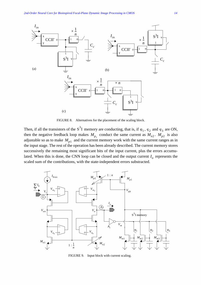
A new problem arises related with the placement of the scaling block in the signal path. Thereare several alternatives. First, the scaling block, the binary weighted current mirror, can beplaced after the offset cancellation memory, as in Fig. 8(a). The problem is that any offset intro-duced by the scaling block is incorporated to the signal path without possible cancellation. Thesecond alternative (Fig. 8(b)) is to place the scaling block before the offset cancellation memory.This means that the S3I memory will have to operate over a wider range of currents, thus com-plicating its design and surely degrading its performance. Our choice, depicted in Fig. 8(c) hasbeen to place the scaling block in the memorization loop. The current memory will operate onthe unscaled version of the input current, and any offsets associated with the scaling blocks willbe sensed and memorized to be cancelled on-line during the network evolution.
The resulting CNN core is shown in Fig. 9 [19]. In this picture, the voltage reference gener-ated with the current conveyor, the current mirrors and the memory can be easily identified.The inverter, , driving the gates of the transistors of the current memory is required for sta-bility. Without it, the output node, , will diverge from the equilibrium. The operation of thiscircuit is as follows. Before running the CNN dynamics, the current offsets of all the synapsesare injected to the virtual reference at node . This current is scaled down to one of itsvalue by means of the adjustable current mirror formed by and . The arrow over stands for the binary programmability of this device. The value of is:
(25)
22.5µA/V87.4ns
2 25.9× 51.8µm2= 1:16
1% 32 32×
Io 1 b0 2b1 4b2 8b3+ + + +( )Iin
16------=
b0 b1 b2 b3τ1 τ2
S3IAi
A
L n-thMn1 Mn2 Mn2
nn 1 b0 2b1 4b2 8b3+ + + +=
2nd-Order Neural Core for Bioinspired Focal-Plane Dynamic Image Processing in CMOS 14
Then, if all the transistors of the memory are conducting, that is, if , and are ON,then the negative feedback loop makes conduct the same current as . is alsoadjustable so as to make and the current memory work with the same current ranges as inthe input stage. The rest of the operation has been already described. The current memory storessuccessively the remaining most significant bits of the input current, plus the errors accumu-lated. When this is done, the CNN loop can be closed and the output current represents thescaled sum of the contributions, with the state-independent errors substracted.
FIGURE 8. Alternatives for the placement of the scaling block.
Iin
CCII-
S3I
Cc
x
yz
i
v
Iin
CCII-
S3I 1
n---×
Cc
x
yz
i
v
Iin
CCII-
S3I
1n---×
Cc
x
yz
i
v
(a) (b)
(c)
1n---×
i o
i o
i o oi
n×
FIGURE 9. Input block with current scaling.
L
A
Mm1 Mm2 Mm3
Mn2
Mp1Mp2
Mn1
1 : n
1 : 1n---
Ik k∑
Vn0Vn0
Vw0Vw0
Ibias
Io
Vo
Vpp
Vnn
Vm
Vi
S3I memory
φ1 φ2 φ3
Ai
S3I φ1 φ2 φ3Mp2
Mn2 Mp2Mp1
Io
2nd-Order Neural Core for Bioinspired Focal-Plane Dynamic Image Processing in CMOS 15
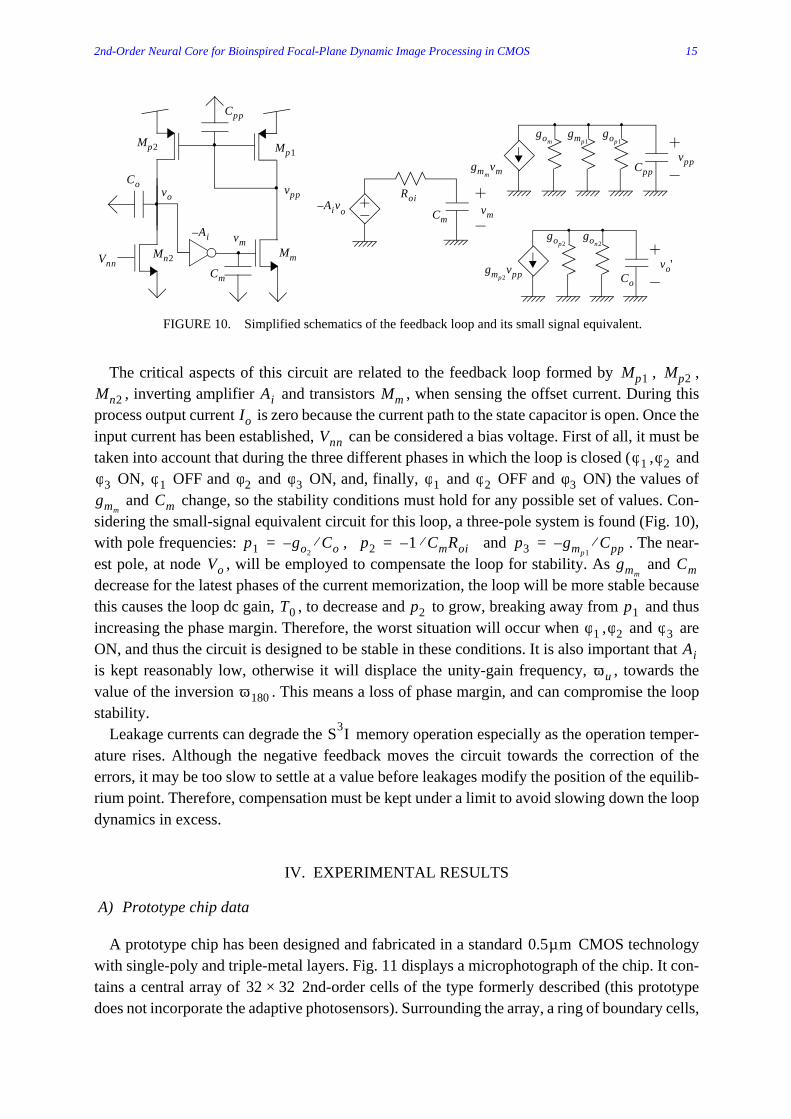
The critical aspects of this circuit are related to the feedback loop formed by , ,, inverting amplifier and transistors , when sensing the offset current. During this
process output current is zero because the current path to the state capacitor is open. Once theinput current has been established, can be considered a bias voltage. First of all, it must betaken into account that during the three different phases in which the loop is closed ( , and
ON, OFF and and ON, and, finally, and OFF and ON) the values of and change, so the stability conditions must hold for any possible set of values. Con-
sidering the small-signal equivalent circuit for this loop, a three-pole system is found (Fig. 10),with pole frequencies: , and . The near-est pole, at node , will be employed to compensate the loop for stability. As and decrease for the latest phases of the current memorization, the loop will be more stable becausethis causes the loop dc gain, , to decrease and to grow, breaking away from and thusincreasing the phase margin. Therefore, the worst situation will occur when , and areON, and thus the circuit is designed to be stable in these conditions. It is also important that is kept reasonably low, otherwise it will displace the unity-gain frequency, , towards thevalue of the inversion . This means a loss of phase margin, and can compromise the loopstability.
Leakage currents can degrade the memory operation especially as the operation temper-ature rises. Although the negative feedback moves the circuit towards the correction of theerrors, it may be too slow to settle at a value before leakages modify the position of the equilib-rium point. Therefore, compensation must be kept under a limit to avoid slowing down the loopdynamics in excess.
IV. EXPERIMENTAL RESULTS
A) Prototype chip data
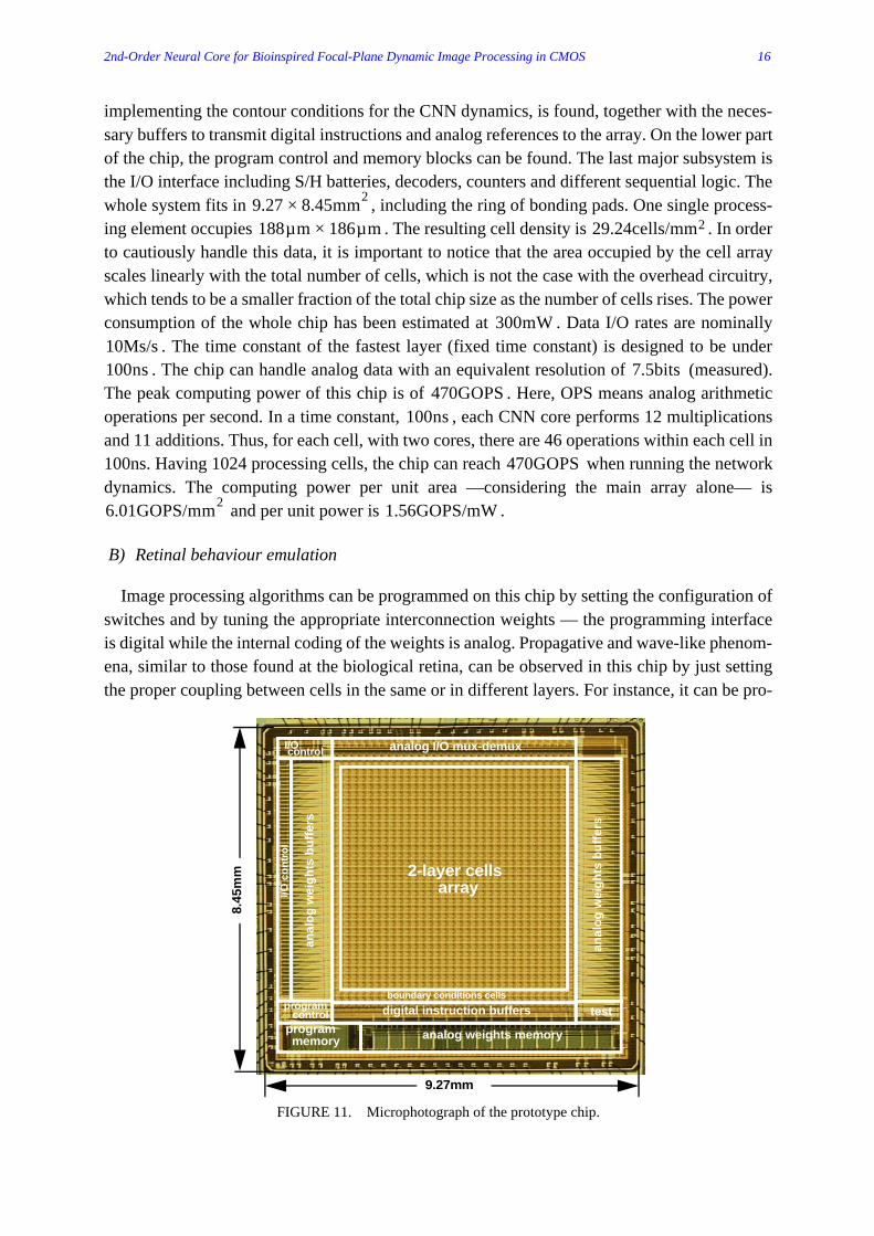
A prototype chip has been designed and fabricated in a standard CMOS technologywith single-poly and triple-metal layers. Fig. 11 displays a microphotograph of the chip. It con-tains a central array of 2nd-order cells of the type formerly described (this prototypedoes not incorporate the adaptive photosensors). Surrounding the array, a ring of boundary cells,
Mp1 Mp2Mn2 Ai Mm
IoVnn
φ1 φ2φ3 φ1 φ2 φ3 φ1 φ2 φ3gmm
Cm
FIGURE 10. Simplified schematics of the feedback loop and its small signal equivalent.
MmMn2
Mp1Mp2
Vnn
vovpp
vmA– i
Cm
Cpp
Co
vo'
Aiv– o
Roi
Cm
Cogmp2
vpp
gop2gon2
gmmvm
vm
vpp
gmp1gop1
gom
Cpp
p1 g– o2Co⁄= p2 1– CmRoi⁄= p3 g– mp1
Cpp⁄=Vo gmm
Cm
T0 p2 p1φ1 φ2 φ3
Aiωu
ω180
S3I
0.5µm
32 32×
2nd-Order Neural Core for Bioinspired Focal-Plane Dynamic Image Processing in CMOS 16
implementing the contour conditions for the CNN dynamics, is found, together with the neces-sary buffers to transmit digital instructions and analog references to the array. On the lower partof the chip, the program control and memory blocks can be found. The last major subsystem isthe I/O interface including S/H batteries, decoders, counters and different sequential logic. Thewhole system fits in , including the ring of bonding pads. One single process-ing element occupies . The resulting cell density is . In orderto cautiously handle this data, it is important to notice that the area occupied by the cell arrayscales linearly with the total number of cells, which is not the case with the overhead circuitry,which tends to be a smaller fraction of the total chip size as the number of cells rises. The powerconsumption of the whole chip has been estimated at . Data I/O rates are nominally
. The time constant of the fastest layer (fixed time constant) is designed to be under. The chip can handle analog data with an equivalent resolution of (measured).
The peak computing power of this chip is of . Here, OPS means analog arithmeticoperations per second. In a time constant, , each CNN core performs 12 multiplicationsand 11 additions. Thus, for each cell, with two cores, there are 46 operations within each cell in100ns. Having 1024 processing cells, the chip can reach when running the networkdynamics. The computing power per unit area —considering the main array alone— is
and per unit power is .
B) Retinal behaviour emulation
Image processing algorithms can be programmed on this chip by setting the configuration ofswitches and by tuning the appropriate interconnection weights — the programming interfaceis digital while the internal coding of the weights is analog. Propagative and wave-like phenom-ena, similar to those found at the biological retina, can be observed in this chip by just settingthe proper coupling between cells in the same or in different layers. For instance, it can be pro-
FIGURE 11. Microphotograph of the prototype chip.
2-layer cellsarray
anal
og
wei
gh
ts b
uff
ers
anal
og
wei
gh
ts b
uff
ers
analog I/O mux-demux
analog weights memoryprogrammemory
digital instruction buffersprogramcontrol
I/O
I/O c
on
tro
l
boundary conditions cells
9.27mm
8.45
mm
control
test
9.27 8.45mm2×188µm 186µm× 29.24cells/mm2
300mW10Ms/s100ns 7.5bits
470GOPS100ns
470GOPS
6.01GOPS/mm2 1.56GOPS/mW
2nd-Order Neural Core for Bioinspired Focal-Plane Dynamic Image Processing in CMOS 17
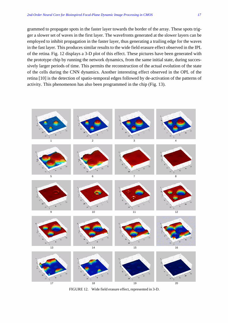
grammed to propagate spots in the faster layer towards the border of the array. These spots trig-ger a slower set of waves in the first layer. The wavefronts generated at the slower layers can beemployed to inhibit propagation in the faster layer, thus generating a trailing edge for the wavesin the fast layer. This produces similar results to the wide field erasure effect observed in the IPLof the retina. Fig. 12 displays a 3-D plot of this effect. These pictures have been generated withthe prototype chip by running the network dynamics, from the same initial state, during succes-sively larger periods of time. This permits the reconstruction of the actual evolution of the stateof the cells during the CNN dynamics. Another interesting effect observed in the OPL of theretina [10] is the detection of spatio-temporal edges followed by de-activation of the patterns ofactivity. This phenomenon has also been programmed in the chip (Fig. 13).
1 2 3 4
5 6 7 8
9 10 12
13 14 15 16
17 18 19 20
11
FIGURE 12. Wide field erasure effect, represented in 3-D.

2nd-Order Neural Core for Bioinspired Focal-Plane Dynamic Image Processing in CMOS 18
1 2 3 4
5 6 7 8
9 10 29
30 31 32 33
34 35 36 37
38 39 40 41
42 43 44 45
FIGURE 13. Spatio-temporal edge detection and de-activation (fast layer).
2nd-Order Neural Core for Bioinspired Focal-Plane Dynamic Image Processing in CMOS 19
V. CONCLUSIONS
Based on a simple but precise model of the real biological system, a feasible efficient imple-mentation of an artificial vision device has been designed. Tailored analog building blocks forfully programmable focal-plane image processing are provided. A prototype chip containing anetwork of CNN nodes have been designed, fabricated and successfully tested instandard CMOS technologies. Different wave-computing algorithms can be implemented in thischip by simply programming the network dynamics with only a few parameters: connectionweights, time constant ratio, bias map and boundary conditions.
ACKNOWLEDGEMENTS
This work has been partially supported by projects IST2001 – 38097 (LOCUST), TIC2003 –09817 - C02 – 01 (VISTA), and ONR-NICOP N000140210884. The authors deeply appreciatethe many useful and fruitful discussions with G. Liñán related to chip architecture and circuitdesign, T. Serrano-Gotarredona regarding the implementation of programmable current mirrorsand with D. Bálya, P. Földesy and I. Petrás related to the experiments.
REFERENCES
[1] B. Roska and F.S. Werblin, “Vertical interactions across ten parallel, stacked representa-tions in the mammalian retina“. Nature, Vol. 410, pp. 583-587, March 2001.
[2] V. Brajovic, “A Model for Reflectance Perception in Vision”. Bioengineered and Bioin-spired Systems, Proceedings of SPIE, Vol. 5119, pp. 307-315, May 2003.
[3] Alireza Moini, Vision Chips. Kluwer Academic Publishers, Boston, 1999.
[4] T. Roska and L. O. Chua: “The CNN Universal Machine: An Analogic Array Computer”.IEEE Transactions on circuits and Systems-II: Analog and Digital Signal Processing, Vol.40, No. 3, pp. 163-173, March 1993.
[5] Cs. Rekeczky, T. Roska, and A. Ushida, “CNN-based Difference-controlled Adaptive Non-linear Image Filters”. International Journal of Circuit Theory and Applications, Vol. 26,pp. 375-423, July-August, 1998.
[6] D. Balya, Cs. Rekeczky and T. Roska, “Basic Mammalian Retinal Effects on the PrototypeComplex Cell CNN Universal Machine”. Proceedings of the 7th IEEE International Work-shop on Cellular Neural Networks and their Applications, pp. 251-258, 2002. Frankfurt amMain, Germany, July 2002.
[7] F. Werblin, “Synaptic Connections, Receptive Fields and Patterns of Activity in the TigerSalamander Retina”. Investigative Ophthalmology and Visual Science, Vol. 32, No. 3,pp. 459-483, March 1991.
[8] H. Wassle and B.B Boycott, “Functional Architecture of the Mammalian Retina”. Physio-logical Reviews, Vol. 71, No. 2. pp. 447-447, 1991.
[9] F. Werblin, T. Roska and L. O. Chua, “The Analogic Cellular Neural Network as a BionicEye”. International Journal of Circuit Theory and Applications, Vol. 23, No. 6, pp. 541-69,November-December 1995.
32 32 2××

2nd-Order Neural Core for Bioinspired Focal-Plane Dynamic Image Processing in CMOS 20
[10]Cs. Rekeczky, B. Roska, E. Nemeth and F. Werblin, “Neuromorphic CNN Models for Spa-tio-Temporal Effects Measured in the Inner and Outer Retina of Tiger Salamander”. Proc.of the Sixth IEEE International Workshop on Cellular Neural Networks and their Applica-tions, pp. 15-20, Catania, Italy, May 2000.
[11]Cs. Rekeczky, T. Serrano-Gotarredona, T. Roska and A. Rodríguez-Vázquez, “A StoredProgram 2nd Order/3-Layer Complex Cell CNN-UM”. Proc. of the Sixth IEEE Internation-al Workshop on Cellular Neural Networks and their Applications, pp. 219-224, Catania, It-aly, May 2000.
[12]S. Espejo, R. Carmona, R. Domínguez-Castro and A. Rodríguez-Vázquez, “A VLSI Ori-ented Continuous-Time CNN Model”. International Journal of Circuit Theory and Appli-cations, John Wiley & Sons. Vol. 24, No. 3, pp. 341-356, May-June 1996.
[13]Y. P. Tsividis, “Integrated Continuous-Time Filter Design —An Overview”. IEEE Journalof Solid-State Circuits, Vol. 29, No. 3, pp. 166-176, March 1994.
[14]R. Domínguez-Castro, A. Rodríguez-Vázquez, S. Espejo and R. Carmona, “Four-QuadrantOne-Transistor Synapse for High Density CNN Implementations”. Proc. of the Fifth IEEEInternational Workshop on Cellular Neural Networks and their Applications, pp. 243-248,London, UK, April 1998.
[15]A. Rodríguez-Vázquez, E. Roca, M. Delgado-Restituto, S. Espejo and R. Domínguez-Cas-tro, “MOST-Based Design and Scaling of Synaptic Interconnections in VLSI Analog ArrayProcessing Chips”. Journal of VLSI Signal Processing Systems for Signal, Image and VideoTechnology, Vol. 23, pp. 239-266, Kluwer Academics, November/December 1999.
[16]K. C. Smith and A. S. Sedra: “The Current Conveyor —A New Circuit Building Block”.IEEE Proceedings, Vol. 56, pp. 1368-1369, August 1968.
[17]C. Toumazou, J. B. Hughes and N. C. Battersby (Eds.), Switched-Currents: An AnalogueTechnique for Digital Technology. Peter Peregrinus, London, England, 1993.
[18]T. Serrano and B. Linares-Barranco: “The Active-Input Regulated-Cascode Current Mir-ror”. IEEE Transactions on circuits and Systems-I: Fundamental Theory and Applications,Vol. 41, No. 6, pp. 464-467, June 1994.
[19]Ricardo Carmona, Analysis and Design of CNN-based VLSI Hardware for Real-Time Im-age Processing. Ph. D. Thesis, University of Seville, June 2002.