25Gb/s 1V-driving CMOS ring modulator with integrated ...
14
YONSEI UNIVERSITY YONSEI UNIVERSITY 25Gb/s 1V-driving CMOS ring modulator with integrated thermal tuning Kim, Sungjin
Transcript of 25Gb/s 1V-driving CMOS ring modulator with integrated ...

YONSEI UNIVERSITY
YONSEI UNIVERSITY
25Gb/s 1V-driving CMOS ring modulator with
integrated thermal tuning
Kim, Sungjin
YONSEI UNIVERSITY
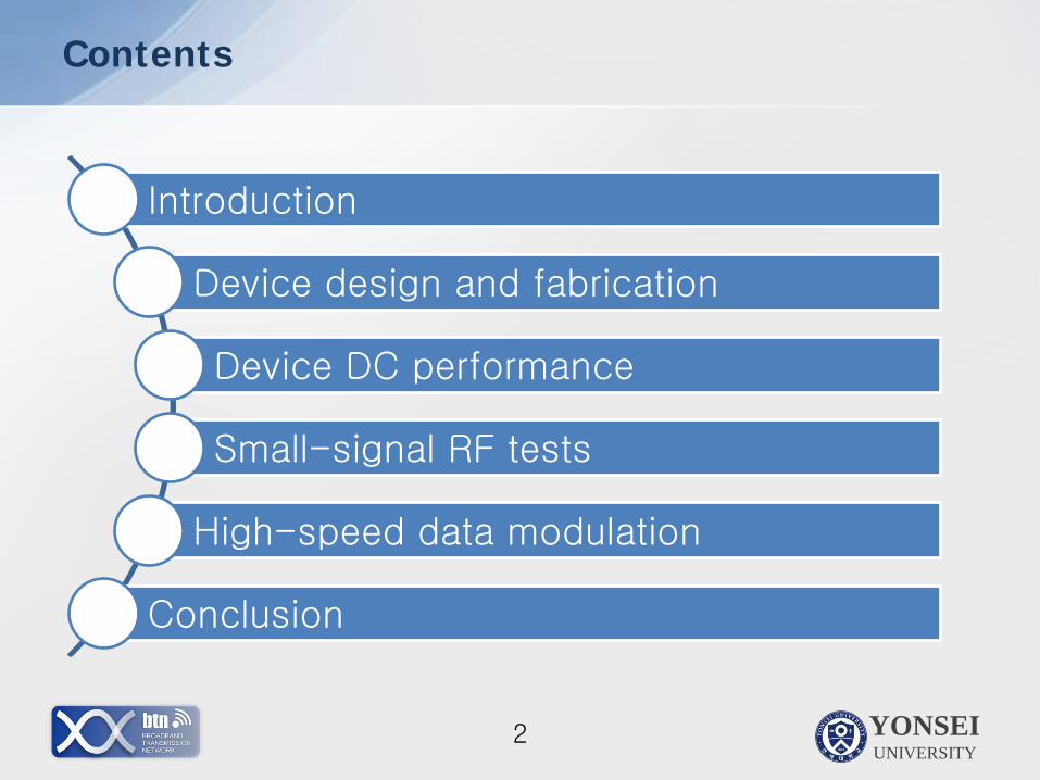
Contents
2
Introduction
Device design and fabrication
Device DC performance
Small-signal RF tests
High-speed data modulation
Conclusion

YONSEI UNIVERSITY
Introduction
3
Carrier-depletion Si ring modulators with thermal tuning
Advantages
- High speed modulation
- consuming low energy for modulation
Disadvantages
- Additional power consumptions occur in thermal tuning
→ Advanced manufacturing techniques and higher modulation speed
can reduce this penalty
Interconnect power and density issues are the
main obstacles for supercomputing
Silicon photonics is candidates incoming
systems
YONSEI UNIVERSITY
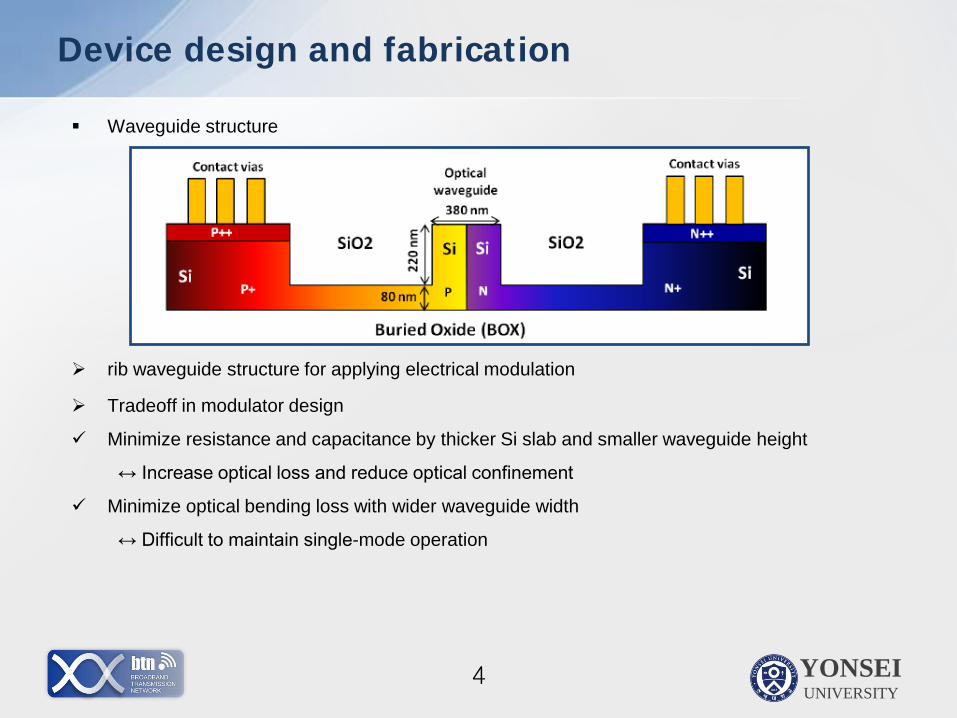
Waveguide structure
rib waveguide structure for applying electrical modulation
Tradeoff in modulator design
Minimize resistance and capacitance by thicker Si slab and smaller waveguide height
↔ Increase optical loss and reduce optical confinement
Minimize optical bending loss with wider waveguide width
↔ Difficult to maintain single-mode operation
Device design and fabrication
4
YONSEI UNIVERSITY
Ring waveguide dimensions
- 7.6μm ring radius to achieve 12.8nm of free spectral range for 8-wavelength-channel WDM link
- 380nm wide ring waveguide with 220nm etch depth and 80nm thick Si slab
- 300nm wide bus waveguide
PN junction doping
- symmetric lateral PN junction
- vertically uniform doping
- laterally increasing density from junction
- to achieve small capacitance, resistance, optical loss
- caution with impurities diffusion occurred during implantations
and multiple CMOS thermal cycles
Device design and fabrication
5
YONSEI UNIVERSITY
Doping profile
The impurity densities decrease linearly from 𝑁𝑑 to zero at the center of the junction
PN junction doping determines the depletion width
→ impact to the modulation depth and optical loss
→ determines the quality factor and modulation bandwidth
Impact of the junction doping to the modulation depth
∆𝜆𝑠𝑠𝑠𝑠𝑠∆𝜆𝐹𝐹𝐹𝐹
∝ 𝑁𝑑1 3⁄
𝛼𝑑𝑑𝑑+𝛼𝑑𝑠𝑠𝑜𝑜 , 𝑤𝑤𝑤𝑤𝑤 𝛼𝑑𝑑𝑑 ∝ 𝑁𝑑
∆𝜆𝑠𝑠𝑠𝑠𝑠 ∶ 𝑡𝑤𝑤 𝑤𝑤𝑟𝑟𝑟𝑟𝑟𝑟𝑤 𝑤𝑟𝑤𝑤𝑤𝑤𝑟𝑤𝑡𝑤 𝑟𝑤𝑠𝑠𝑡 𝑢𝑟𝑢𝑤𝑤 𝑤𝑟𝑤𝑡𝑟𝑤𝑤 𝑟𝑤𝑠𝑟𝑤
Δ𝜆𝐹𝐹𝐹𝐹 ∶ 𝑠𝑢𝑤𝑤 𝑤𝑠𝑢𝑡𝑤 𝑟𝑡 𝑤𝑟𝑤𝑠 𝑚𝑟𝑚𝑠𝑚𝑢𝑚 𝑟𝑠 𝑡𝑤𝑤 𝑤𝑤𝑟𝑟𝑟𝑟𝑟𝑟𝑤 𝑤𝑠𝑢𝑡𝑤
𝛼𝑑𝑑𝑑 ∶ 𝑤𝑟𝑟𝑟 𝑟𝑟𝑤𝑠𝑠𝑠𝑟𝑠𝑤𝑟𝑡 𝑢𝑢𝑤 𝑡𝑟 𝑗𝑢𝑟𝑟𝑡𝑠𝑟𝑟 𝑢𝑟𝑑𝑠𝑟𝑤,𝛼𝑑𝑠𝑠𝑜𝑜 ∶ 𝑤𝑟𝑟𝑟 𝑟𝑟𝑤𝑠𝑠𝑠𝑟𝑠𝑤𝑟𝑡 𝑢𝑢𝑤 𝑡𝑟 𝑟𝑡𝑤𝑤𝑤 𝑚𝑤𝑟𝑤𝑟𝑟𝑠𝑟𝑚𝑟
- to maximize modulation depth, 𝛼𝑑𝑑𝑑 = 0.5𝛼𝑑𝑠𝑠𝑜𝑜
- typical 𝛼𝑑𝑠𝑠𝑜𝑜 is 6dB/cm, which requires junction doping of 3 × 10¹⁷𝑟𝑚−3
Device design and fabrication
6

YONSEI UNIVERSITY
Modulation bandwidth
Bandwidth is proportional to the waveguide loss
𝑠𝑑 = 𝑐𝛼 𝜋𝑛𝑔⁄
- maximized modulation depth results in small bandwidth of 5GHz
- to achieve higher modulation bandwidth, increase the junction doping density
and sacrifice the modulation depth
- to have 𝑠𝑑 > 25𝐺𝐺𝐺
𝑄 < 8000
𝜆𝑠𝑠𝑠𝑠𝑠 > 40𝑑𝑚
𝑚𝑟𝑢𝑢𝑤𝑟𝑡𝑟𝑤 𝑑𝑤𝑟𝑟𝑤𝑡𝑝 > 9𝑢𝑑
Device design and fabrication
7
YONSEI UNIVERSITY
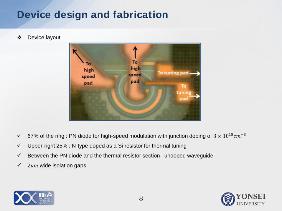
Device layout
67% of the ring : PN diode for high-speed modulation with junction doping of 3 × 10¹⁸𝑟𝑚−3
Upper-right 25% : N-type doped as a Si resistor for thermal tuning
Between the PN diode and the thermal resistor section : undoped waveguide
2𝜇𝑚 wide isolation gaps
Device design and fabrication
8
YONSEI UNIVERSITY
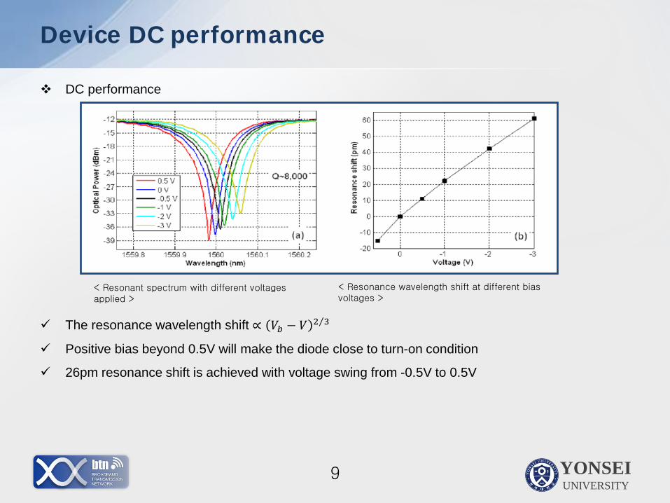
DC performance
The resonance wavelength shift ∝ 𝑉𝑏 − 𝑉 2 3⁄
Positive bias beyond 0.5V will make the diode close to turn-on condition
26pm resonance shift is achieved with voltage swing from -0.5V to 0.5V
Device DC performance
9
< Resonant spectrum with different voltages applied >
< Resonance wavelength shift at different bias voltages >

YONSEI UNIVERSITY
DC performance
750Ω of Si resistor
Tuning efficiency of 0.19nm/mW
66mW tuning power is needed to tune the 12.6nm FSR
Device DC performance
10
< Resonant spectrum with different tuning power applied >
< Resonance wavelength versus tuning power >

YONSEI UNIVERSITY
Circuit model
High-speed behavior of the ring modulator can be approximated by circuit model
𝐶𝑑 : capacitance between the electrodes through top dielectrics
𝑅𝑆 and 𝐶𝐽 : model the current path through the reverse-biased PN junction
𝑅𝑆𝑠 and 𝐶𝑂𝑂 : model the current path through the BOX and the Si handle
Based on the circuit model, modulation energy is 7fJ/bit with 25Gb/s pseudo-random data
Small-signal RF tests
11
< fitted circuit model > < curve-fitting using the circuit model>

YONSEI UNIVERSITY
Experimental results
High-speed data modulation
12
Eye-diagram with 25Gb/s modulation 1Vpp voltage swing
>5dB extinction ratio
Laser wavelength is tuned over the
5.3nm

YONSEI UNIVERSITY
Demonstrated an error-free 25Gb/s tunable carrier-depletion ring
modulator with 7.5μm radius
Small junction capacitance leads to 7fJ/bit modulation energy with 1V
driving at 25Gb/s
The carrier-depletion Si ring modulators can enable ultrahigh-speed
and ultralow-power WDM photonic links with compact footprint
Conclusion
13

YONSEI UNIVERSITY
14