256 Low-Cost FPGAs - Altera · Low-Cost FPGAs Subscribe Send Feedback AN-754 ... FPGA Receiving...
25
AN 754: MIPI D-PHY Solution with Passive Resistor Networks in Intel ® Low-Cost FPGAs Subscribe Send Feedback AN-754 | 2017.11.20 Latest document on the web: PDF | HTML
Transcript of 256 Low-Cost FPGAs - Altera · Low-Cost FPGAs Subscribe Send Feedback AN-754 ... FPGA Receiving...

AN 754: MIPI D-PHY Solution withPassive Resistor Networks in Intel®Low-Cost FPGAs
SubscribeSend Feedback
AN-754 | 2017.11.20Latest document on the web: PDF | HTML

Contents
AN 754: MIPI D-PHY Solution with Passive Resistor Networks in Intel® Low-CostFPGAs........................................................................................................................ 3Introduction to MIPI D-PHY........................................................................................... 3Overview on MIPI Operation.......................................................................................... 3Functional Description: FPGA Receiving Interface and FPGA Transmitting Interface................4I/O Standards for MIPI D-PHY Implementation.................................................................6MIPI D-PHY Specifications............................................................................................. 6
MIPI D-PHY Specifications for Receiver...................................................................6MIPI D-PHY Specifications for Transmitter...............................................................7
FPGA I/O Standard Specifications...................................................................................8FPGA I/O Standard Specifications for MIPI Receiver................................................. 8FPGA I/O Standard Specifications for MIPI Transmitter.............................................9
IBIS Simulation........................................................................................................... 9FPGA As Receiver: HS-RX and LP-RX Modes Simulation.......................................... 10FPGA As Receiver: Simulation Results.................................................................. 10FPGA As Transmitter: HS-TX and LP-TX Modes Simulation.......................................17FPGA As Transmitter: Simulation Results.............................................................. 18
PCB Design Guidelines................................................................................................ 23Conclusion................................................................................................................ 24Document Revision History for AN 754: MIPI D-PHY Solution with Passive Resistor
Networks in Intel Low-Cost FPGAs....................................................................... 25
Contents
AN 754: MIPI D-PHY Solution with Passive Resistor Networks in Intel® Low-Cost FPGAs2

AN 754: MIPI D-PHY Solution with Passive ResistorNetworks in Intel® Low-Cost FPGAs
Introduction to MIPI D-PHY
The Mobile Industry Processor Interface (MIPI) is an industry consortium specifyinghigh-speed serial interface solutions to interconnect between components inside amobile device. The group specifies both protocols and physical layer standards for avariety of applications. The D-PHY is a popular MIPI physical layer standard forCamera Serial Interface (CSI-2) and Display Serial Interface (DSI) protocols. You canuse the CSI-2 interface with D-PHY for the Camera (Imager) to Host interface, as astreaming video interface between devices, and in applications outside of mobiledevices.
Overview on MIPI Operation
The D-PHY provides a synchronous connection between a master and slave. Theminimum PHY configuration consists of a clock and one or more data signals. The D-PHY uses two wires per data lane and two wires for the clock lane. The lane canoperate in a high-speed (HS) signaling mode for fast-data traffic and low-power (LP)signaling mode for control purpose.
The maximum data rate that can be supported in high-speed signaling is determinedby the performance of the transmitter, receiver, and interconnect implementations. Inpractice, the typical implementation has a bit rate of approximately 500-800 Mbps perlane in high-speed mode for passive D-PHY. However, for some D-PHY applications,the bit rate can go up to 1.5 Gbps per lane. The maximum data rate in low-powermode is 10 Mbps.
The three possible implementations for connecting MIPI / D-PHY compliant device toIntel FPGAs are as follows:
• Use of an external D-PHY ASSP (for example Meticom MC2000x and MC2090xdevices) as an active level shifter
• Use passive resistor network to create the compatible D-PHY with FPGA general-purpose I/O (GPIO)
• Use FPGA transceiver I/O to achieve higher data rate
This application note discusses the implementation using passive resistor network toachieve the lowest cost implementation.
The D-PHY can support bidirectional data transmission or unidirectional datatransmission. CSI-2 protocol only requires unidirectional data transmission. Thus thisimplementation of a MIPI D-PHY compatible solution for Intel’s low cost FPGAs onlysupports unidirectional data transmission.
AN-754 | 2017.11.20
Intel Corporation. All rights reserved. Intel, the Intel logo, Altera, Arria, Cyclone, Enpirion, MAX, Nios, Quartusand Stratix words and logos are trademarks of Intel Corporation or its subsidiaries in the U.S. and/or othercountries. Intel warrants performance of its FPGA and semiconductor products to current specifications inaccordance with Intel's standard warranty, but reserves the right to make changes to any products and servicesat any time without notice. Intel assumes no responsibility or liability arising out of the application or use of anyinformation, product, or service described herein except as expressly agreed to in writing by Intel. Intelcustomers are advised to obtain the latest version of device specifications before relying on any publishedinformation and before placing orders for products or services.*Other names and brands may be claimed as the property of others.
ISO9001:2008Registered

• Receiving interface—FPGA I/O receives the high-speed or low-power signalingfrom a MIPI D-PHY transmitter (TX) device such as camera sensor or imager
• Transmitting interface—FPGA I/O transmits the high-speed or low-power signalingto a MIPI D-PHY receiver (RX) device such as a host or display
The high-speed differential signaling and low-power single-ended serial signals havedifferent electrical characteristics. This application note covers the recommendation ofthe I/O standard for the FPGA I/O to emulate a MIPI D-PHY RX or TX, and provide anelectrically compatibility between FPGA I/O and the MIPI interface. The single-endedmode uses LVCMOS or HSTL I/O standard for low-power mode, and differential I/Ostandard (LVDS) for high-speed mode. Resistors are used to connect, isolate,terminate, and level set to construct the compatible D-PHY.
Functional Description: FPGA Receiving Interface and FPGATransmitting Interface
MIPI D-PHY IP incorporated in the FPGA is able to receive and transmit serial datawhich consists of one clock and one or more data lanes. The data lanes can switchbetween the high-speed and low-power signaling through a passive resistor network inunidirectional mode as shown in the following figures. This may be a spate IP block orintegrated into the MIPI CSI-2 protocol controllers depending on the IP source orthird-party IP partner. The lane control and interface logic are essential to the D-PHYfunctionality that needs to be built inside the FPGA logic.
Figure 1. FPGA Unidirectional Receiver Implementation Block DiagramThis figure shows high-speed and low-power modes in a single lane and common resistor configuration.
MIPI D-PHYTX Device(such as
camera sensor)
High Speed
Low Power
Passive Resistor Network
Lane Controland Interface
Logic
MIPI D-PHY ModuleReceiver FPGA
Rx Ω
Ry Ω
AN 754: MIPI D-PHY Solution with Passive Resistor Networks in Intel® Low-Cost FPGAs
AN-754 | 2017.11.20
AN 754: MIPI D-PHY Solution with Passive Resistor Networks in Intel® Low-Cost FPGAs4

Figure 2. FPGA Unidirectional Transmitter Implementation Block Diagram
This figure shows high-speed and low-power modes in a single lane and common resistor configuration.
When the interface is in high-speed mode, the MIPI D-PHY RX device presents a 100 Ω differential termination.When the common-mode of the lines indicates that the interface is in low-power mode, the 100 Ω terminationis switched to high Z.
MIPI D-PHYRX Device(such as
host/display)
Lane Controland Interface
Logic
MIPI D-PHY ModuleTransmitter FPGA
zz Ω xx Ω
zz Ω
yy Ω
Passive Resistor Network
High Speed
Low Power
Related Links
MIPI CSI-2 Controller CoreProvides more information about MIPI CSI-2 Controller Core
AN 754: MIPI D-PHY Solution with Passive Resistor Networks in Intel® Low-Cost FPGAs
AN-754 | 2017.11.20
AN 754: MIPI D-PHY Solution with Passive Resistor Networks in Intel® Low-Cost FPGAs5

I/O Standards for MIPI D-PHY Implementation
Table 1. I/O Standards for MIPI D-PHY ImplementationThis table lists the I/O standards supported for the FPGA I/O buffer for the MIPI D-PHY implementation in high-speed or low-power RX or TX mode. The recommendation has selected such that the following I/Os can co-exist in an I/O bank depending on the FPGA device.
• High-speed
• Low-power
• High-speed and low-power
Device FPGA I/OBuffer Mode
SignalingMode
I/O Standard I/O Voltage Supply (V)
Input Output
Cyclone® IV GX,Cyclone V,Intel® MAX® 10
RX High-speed LVDS (1) 2.5 (2) —
Low-power HSTL-12 (1), 1.2 V LVCMOS 2.5 (2), 1.2 —
TX High-speed Differential HSTL-18 (3) — 1.8
Low-power 1.8 V LVCMOS (3), 2.5 VLVCMOS
— 1.8, 2.5
MIPI D-PHY Specifications
MIPI D-PHY Specifications for Receiver
Table 2. High-Speed MIPI D-PHY Receiver DC SpecificationsThis table shows the MIPI D-PHY receiver high-speed signal DC specifications as stipulated in the MIPI D-PHYspecifications from the MIPI Alliance.
Parameter Description Minimum Typical Maximum Unit
VCMRX(DC) Common-mode voltage high-speedreceive mode
70 — 330 mV
VIDTH Differential input high threshold — — 70 mV
VIDTL Differential input low threshold –70 — — mV
VIHHS Single-ended input high voltage — — 460 mV
VILHS Single-ended input low voltage –40 — — mV
VTERM-EN Single-ended threshold for high-speedtermination enable
— — 450 mV
ZID Differential input impedance 80 100 125 Ω
(1) The LVDS can co-exist in the same I/O bank as HSTL-12 when the FPGA is configured as inputbuffer in Cyclone V devices.
(2) Input buffer for LVDS and HSTL-12 I/O standards are powered by VCCPD in Cyclone V devices.
(3) The Differential HSTL-18 can co-exist in the same I/O bank as 1.8 V LVCMOS when the FPGAis configured as output buffer in Cyclone IV GX, Cyclone V, and Intel MAX 10 devices.
AN 754: MIPI D-PHY Solution with Passive Resistor Networks in Intel® Low-Cost FPGAs
AN-754 | 2017.11.20
AN 754: MIPI D-PHY Solution with Passive Resistor Networks in Intel® Low-Cost FPGAs6

Table 3. Low-Power MIPI D-PHY Receiver DC SpecificationsThis table shows the MIPI D-PHY receiver low-power signal DC specifications as stipulated in the MIPI D-PHYspecifications from the MIPI Alliance.
Parameter Description Minimum Typical Maximum Unit
VIH Logic 1 input voltage 880 — — mV
VIL Logic 0 input voltage, not in ultra lowpower (ULP) state
— — 550 mV
MIPI D-PHY Specifications for Transmitter
Table 4. High-Speed MIPI D-PHY Transmitter DC SpecificationsThis table shows the MIPI D-PHY transmitter high-speed signal DC specifications as stipulated in the MIPI D-PHY specifications from the MIPI Alliance.
Parameter Description Minimum Typical Maximum Unit
VCMTX High-speed transmit static common-modevoltage (4)
150 200 250 mV
|ΔVCMTX(1,0)| VCMTX mismatch when output isDifferential-1 or Differential-0 (5)
— — 5 mV
|VOD| High-speed transmit differentialvoltage (4)
140 200 270 mV
|ΔVOD| VOD mismatch when output isDifferential-1 or Differential-0 (5)
— — 10 mV
VOHHS High-speed output high voltage (4) — — 360 mV
ZOS Single-ended output impedance 40 50 62.5 Ω
ΔZOS Single-ended output impedancemismatch
— — 10 %
Table 5. Low-Power MIPI D-PHY Transmitter DC SpecificationsThis table shows the MIPI D-PHY transmitter low-power signal DC specifications as stipulated in the MIPI D-PHYspecifications from the MIPI Alliance.
Parameter Description Minimum Typical Maximum Unit
VOH Thevenin output high level 1.1 1.2 1.3 V
VOL Thevenin output low level –50 — 50 mV
(4) When driving into load impedance within the ZID range.
(5) Recommended to minimize ΔVOD and ΔVCMTX(1,0) to minimize radiation and optimize signalintegrity.
AN 754: MIPI D-PHY Solution with Passive Resistor Networks in Intel® Low-Cost FPGAs
AN-754 | 2017.11.20
AN 754: MIPI D-PHY Solution with Passive Resistor Networks in Intel® Low-Cost FPGAs7

FPGA I/O Standard Specifications
FPGA I/O Standard Specifications for MIPI Receiver
The DC specifications for 1.2 V LVCMOS, HSTL-12, and LVDS I/O standards are asstipulated in the device datasheets for the respective devices. When an FPGA functionsas a MIPI D-PHY receiver, the transmitted high-speed and low-power signals from theMIPI D-PHY transmitter are expected to meet these FPGA I/O standards specificationswith passive resistor network.
Table 6. 1.2 V LVCMOS I/O Standard DC Specifications
I/OStandard
VCCIO (V) VIL (V) VIH (V)
Min Typ Max Min Max Min Max
1.2 V 1.14 1.2 1.26 –0.3 0.35 × VCCIO 0.65 × VCCIO VCCIO + 0.3
Table 7. Single-Ended HSTL-12 I/O Reference Voltage Specifications
I/OStandard
VCCIO (V) VREF (V) VTT (V)
Min Typ Max Min Typ Max Min Typ Max
HSTL-12Class I, II
1.14 1.2 1.26 0.48 ×VCCIO (6)
0.50 ×VCCIO (6)
0.52 ×VCCIO (6)
— 0.50 ×VCCIO
—
0.47 ×VCCIO (7)
0.50 ×VCCIO (7)
0.53 ×VCCIO (7)
Table 8. Single-Ended HSTL-12 I/O Standard Signal Specifications
I/OStandard
VIL(DC) (V) VIH(DC) (V) VIL(AC) (V) VIH(AC) (V)
Min Max Min Max Min Max Min Max
HSTL-12Class I, II
–0.15 VREF – 0.08 VREF + 0.08 VCCIO+ 0.15
–0.24 VREF – 0.15 VREF + 0.15 VCCIO+ 0.24
Table 9. LVDS I/O Standard DC Specifications
I/OStandard
VCCIO (V) VID (V) VICM (V)
Min Typ Max Min Max Min Condition Max
LVDS 2.375 2.5 2.625 100 — 0.05 DMAX ≤ 500 Mbps 1.8
0.55 500 Mbps ≤ DMAX ≤700 Mbps
1.8
1.05 DMAX > 700 Mbps 1.55
(6) Value shown refers to DC input reference voltage, VREF(DC).
(7) Value shown refers to AC input reference voltage, VREF(AC).
AN 754: MIPI D-PHY Solution with Passive Resistor Networks in Intel® Low-Cost FPGAs
AN-754 | 2017.11.20
AN 754: MIPI D-PHY Solution with Passive Resistor Networks in Intel® Low-Cost FPGAs8

FPGA I/O Standard Specifications for MIPI Transmitter
The DC specifications for Differential HSTL-18, 1.8 V LVCMOS, and 2.5 V LVCMOS I/Ostandards are as stipulated in the device datasheets for the respective devices. Whenan FPGA functions as a MIPI D-PHY transmitter, the transmitted high-speed and low-power signals from the FPGA I/O are expected to meet the high-speed and low-powerMIPI D-PHY receiver specifications with passive resistor network.
Table 10. Differential HSTL-18, 1.8 V LVCMOS, and 2.5 V LVCMOS I/O Standards DCSpecifications
I/O Standard VCCIO (V) VOL (V) VOH (V)
Min Typ Max Max Min
HSTL-18(8) Class I, II 1.71 1.8 1.89 0.4 VCCIO – 0.4
1.8 V LVCMOS 1.71 1.8 1.89 0.45 VCCIO – 0.45
2.5 V LVCMOS 2.375 2.5 2.625 0.4 2
Related Links
MIPI D-PHY Specifications for Receiver on page 6
IBIS Simulation
IBIS simulation using HyperLynx is performed to show the link simulation between theMIPI D-PHY, transmission line, passive resistor network, and FPGA I/O for Cyclone IV,Cyclone V, and Intel Intel MAX 10 devices. The simulation demonstrates the followingsignaling modes with the passive resistor networks setups:
• Input and output differential and common-mode voltage levels for high-speedsignaling
• Single-ended input and output high and low voltage levels for low-power signaling
During normal operation, either high-speed or low-power signaling can drive a lane.The states for high-speed lane are Differential-0 and Differential-1. The two single-ended lines in low-power lane states can drive a different or same state depending onthe mode of operation. The low-power lane can drive four possible states: LP00, LP11,LP01 and LP10.
The high-speed mode is simulated at 840 Mbps for Cyclone IV and Cyclone V devices,and 720 Mbps for Intel MAX 10 device. The low-power mode is simulated at 10 Mbpsfor Cyclone IV, Cyclone V, and Intel MAX 10 devices. The simulation uses simpletransmission line that assumed to have the characteristics impedance of 50 Ω with500 ps transmission delay.
(8) Differential HSTL-18 is a pseudo differential I/O standard consists of two single-ended HSTL-18output buffers. One single-ended output buffer is the P channel and another single-endedoutput buffer is the N channel (inversion of P channel). The output differential signal (VOD) isthe difference of VOH–VOL. The output common mode voltage (VOCM) is the signal crossingpoint for P and N channels.
AN 754: MIPI D-PHY Solution with Passive Resistor Networks in Intel® Low-Cost FPGAs
AN-754 | 2017.11.20
AN 754: MIPI D-PHY Solution with Passive Resistor Networks in Intel® Low-Cost FPGAs9

FPGA As Receiver: HS-RX and LP-RX Modes Simulation
In the HS-RX and LP-RX mode simulation, the FPGA acts as a receiver to receive theMIPI D-PHY high-speed and low-power signals from MIPI D-PHY TX device in a singlelane. The differential termination is fixed at 300 Ω across the LVDS pair in a singlelane. The termination is set high to avoid the complexity of switching in and out of thehigh-speed mode termination. The termination supports the required signal quality atthe targeted data rates although the termination does not match the characteristicsimpedance of the transmission line. The 300 Ω load between the lines minimizesloading in the low-power mode and in the LP01 or LP10 state. The two fixed seriestermination resistors are used for the low-power signals.
Figure 3. FPGA As Receiver HS-RX and LP-RX Modes IBIS Simulation Circuit
TL81
TL82ov5647MDP0 50.0 Ω
500.000 psSimple
50.0 Ω500.000 ps
Simple R162
R163
R164
R165
C12100.0 pF
150.0 Ω
150.0 Ω
100.0 Ω
100.0 Ω
Cyclone IVlvds25_rdinp
Cyclone IVhstl12_cin
Cyclone IVhstl12_cin
MIPI D-PHYTransmitter
TransmissionLine
Board Passive ResistorNetwork Circuit
MIPI D-PHYReceiver FPGA
FPGA As Receiver: Simulation Results
The simulated waveforms for the Cyclone IV, Cyclone V, and Intel MAX 10 devices arebased on the recommended setup. The I/O standards used in the FPGA I/O pins arecompliant to the following voltage levels transmitted from the MIPI D-PHY TX deviceunder typical conditions:
• High-speed signals—Output differential (VOD) and common mode (VOCM) voltagelevels
• Low-power single-ended signals—Output voltage high (VOH) and output voltagelow(VOL) signals
AN 754: MIPI D-PHY Solution with Passive Resistor Networks in Intel® Low-Cost FPGAs
AN-754 | 2017.11.20
AN 754: MIPI D-PHY Solution with Passive Resistor Networks in Intel® Low-Cost FPGAs10

FPGA As Receiver: Simulation Results Using Cyclone IV Devices
Figure 4. HS-RX Mode Eye Diagram Measured At Cyclone IV FPGA Receiver Die At 840MbpsTrue (P) and Inverted (N) signals are plotted in purple and green. The P and N signals are overlapped.Differential signal (P-N) is plotted in yellow.
AN 754: MIPI D-PHY Solution with Passive Resistor Networks in Intel® Low-Cost FPGAs
AN-754 | 2017.11.20
AN 754: MIPI D-PHY Solution with Passive Resistor Networks in Intel® Low-Cost FPGAs11

Figure 5. LP-RX Mode Waveform Measured At Cyclone IV FPGA Receiver Die for LP11and LP00 States at 10 MbpsDP signal is shown in blue and DN signal is shown in pink. The DN signal (pink) overlaps with the DP signal(blue) because both signals are driven on the same state (LP11, LP00).
Figure 6. LP-RX Mode Waveform Measured At Cyclone IV FPGA Receiver Die for LP10and LP01 States at 10 MbpsBoth DP and DN signals are not overlapped because they are driven out of phase (LP10, LP01).
AN 754: MIPI D-PHY Solution with Passive Resistor Networks in Intel® Low-Cost FPGAs
AN-754 | 2017.11.20
AN 754: MIPI D-PHY Solution with Passive Resistor Networks in Intel® Low-Cost FPGAs12

FPGA As Receiver: Simulation Results Using Cyclone V Devices
Figure 7. HS-RX Mode Eye Diagram Measured At Cyclone V FPGA Receiver Die At 840MbpsTrue (P) and Inverted (N) signals are plotted in purple and green. The P and N signals are overlapped.Differential signal (P-N) is plotted in yellow.
AN 754: MIPI D-PHY Solution with Passive Resistor Networks in Intel® Low-Cost FPGAs
AN-754 | 2017.11.20
AN 754: MIPI D-PHY Solution with Passive Resistor Networks in Intel® Low-Cost FPGAs13

Figure 8. LP-RX Mode Waveform Measured At Cyclone V FPGA Receiver Die for LP11and LP00 States at 10 MbpsDP signal is shown in green and DN signal is shown in red. The DN signal (red) overlaps with the DP signal(green) because both signals are driven on the same state (LP11, LP00).
Figure 9. LP-RX Mode Waveform Measured At Cyclone V FPGA Receiver Die for LP10and LP01 States at 10 MbpsBoth DP and DN signals are not overlapped because they are driven out of phase (LP10, LP01).
AN 754: MIPI D-PHY Solution with Passive Resistor Networks in Intel® Low-Cost FPGAs
AN-754 | 2017.11.20
AN 754: MIPI D-PHY Solution with Passive Resistor Networks in Intel® Low-Cost FPGAs14

FPGA As Receiver: Simulation Results Using Intel MAX 10 Devices
Figure 10. HS-RX Mode Eye Diagram Measured At Intel MAX 10 FPGA Receiver Die At720 MbpsTrue (P) and Inverted (N) signals are plotted in yellow and pink. The P and N signals are overlapped.Differential signal (P-N) is plotted in blue.
AN 754: MIPI D-PHY Solution with Passive Resistor Networks in Intel® Low-Cost FPGAs
AN-754 | 2017.11.20
AN 754: MIPI D-PHY Solution with Passive Resistor Networks in Intel® Low-Cost FPGAs15

Figure 11. LP-RX Mode Waveform Measured At Intel MAX 10 FPGA Receiver Die for LP11and LP00 States at 10 MbpsDP signal is shown in blue and DN signal is shown in red. The DN signal (red) overlaps with the DP signal(blue) because both signals are driven on the same state (LP11, LP00).
Figure 12. LP-RX Mode Waveform Measured At Intel MAX 10 FPGA Receiver Die for LP10and LP01 States at 10 MbpsBoth DP and DN signals are not overlapped because they are driven out of phase (LP10, LP01).
AN 754: MIPI D-PHY Solution with Passive Resistor Networks in Intel® Low-Cost FPGAs
AN-754 | 2017.11.20
AN 754: MIPI D-PHY Solution with Passive Resistor Networks in Intel® Low-Cost FPGAs16

FPGA As Transmitter: HS-TX and LP-TX Modes Simulation
In the HS-TX and LP-TX mode simulation, the FPGA acts as a MIPI D-PHY TX device.The MIPI D-PHY RX device is represented by the package parasitic components with aworst case capacitive load of 3.0 pF.
When the interface is in high-speed mode, the MIPI D-PHY RX device presents a 100Ω differential termination in this simulation (as shown in the FPGA As Transmitter HS-TX Mode IBIS Simulation Circuit diagram). When the common-mode of the linesindicates that the interface is in low-power mode, the 100 Ω termination is switched tohigh Z, which is not shown in the LP-TX mode IBIS simulation circuit (as shown in theFPGA As Transmitter LP-TX Mode IBIS Simulation Circuit diagram). In this simulation,the MIPI D-PHY high-speed receiver is turned off during the low-power modeoperation, thus the input differential termination is removed.
The IBIS simulation uses the buffers in different modes as follows:
• High-speed mode
— A differential buffer is used to transmit signals.
— Two single-ended buffers are configured as input mode to act as tri-statedoutputs.
• Low-power mode
— A differential buffer is configured as input mode to act as tri-stated output.
— Two single-ended buffers are used to transmit signals.
Figure 13. FPGA As Transmitter HS-TX Mode IBIS Simulation Circuit
R23960.0 Ω
R237150.0 Ω
R238150.0 Ω
R246100.0 Ω
R247100.0 Ω
R242100.0 Ω
TL112
TL113
Cyclone Vdhst18i_criop_r50c
50.0 Ω500.000 ps
Simple
50.0 Ω500.000 ps
Simple
R236
60.0 ΩC403.9 pF
C423.0 pF
L13 R243
C413.9 pF
C433.0 pF
L14 R244
2.6 nH
2.6 nH351.0 mΩ
351.0 mΩ
MIPI D-PHYTransmitter FPGA
TransmissionLine
Board Passive ResistorNetwork Circuit
MIPI D-PHY Receiver
Cyclone V18_crin
Cyclone V18_crin Package Parasitic RLC
(Worst case capacitive load = 3.0 pF)
AN 754: MIPI D-PHY Solution with Passive Resistor Networks in Intel® Low-Cost FPGAs
AN-754 | 2017.11.20
AN 754: MIPI D-PHY Solution with Passive Resistor Networks in Intel® Low-Cost FPGAs17

Figure 14. FPGA As Transmitter LP-TX Mode IBIS Simulation Circuit
R23960.0 Ω
R237150.0 Ω
R238150.0 Ω
R246100.0 Ω
R247100.0 Ω
TL112
TL113
Cyclone Vdhst18i_criop_r50c
50.0 Ω500.000 ps
Simple
50.0 Ω500.000 ps
Simple
R236
60.0 ΩC403.9 pF
C423.0 pF
L13 R243
C413.9 pF
C433.0 pF
L14 R244
2.6 nH
2.6 nH351.0 mΩ
351.0 mΩ
MIPI D-PHYTransmitter FPGA
TransmissionLine
Board Passive ResistorNetwork Circuit
MIPI D-PHY Receiver
Cyclone V18_crin
Cyclone V18_crin
Package Parasitic RLC(Worst case capacitive load = 3.0 pF)
FPGA As Transmitter: Simulation Results
The simulated waveforms for the Cyclone IV, Cyclone V, and Intel MAX 10 devices arebased on the recommended setup.
The I/O standards used in the FPGA I/O pins are compliant to the following voltagelevels as defined for high-speed or low-power MIPI D-PHY RX device under typicalconditions:
• High-speed signals—Input differential (VID) and common mode (VICM) voltagelevels
• Low-power single-ended signals—Input voltage high (VIH) and input voltage low(VIL) signals
The signal quality for high-speed signal is better with less jitter compared to the high-speed signal when FPGA acts as the receiving interface. The 100 Ω differentialtermination resistor at the load provides good impedance matching to thecharacteristic impedance of the transmission line.
AN 754: MIPI D-PHY Solution with Passive Resistor Networks in Intel® Low-Cost FPGAs
AN-754 | 2017.11.20
AN 754: MIPI D-PHY Solution with Passive Resistor Networks in Intel® Low-Cost FPGAs18

FPGA As Transmitter: Simulation Results Using Cyclone IV Devices
Figure 15. Cyclone IV HS-TX Mode Eye Diagram Measured At MIPI D-PHY Receiver DieAt 840 MbpsTrue (P) and Inverted (N) signals are plotted in purple and blue. Differential signal (P-N) is plotted in green.
Figure 16. Cyclone IV LP-TX Mode Waveform Measured At MIPI D-PHY Receiver Die forLP11 and LP00 States at 10 MbpsDP signal is shown in pink and DN signal is shown in yellow. The DN signal (yellow) overlaps with the DP signal(pink) because both signals are driven on the same state (LP11, LP00).
AN 754: MIPI D-PHY Solution with Passive Resistor Networks in Intel® Low-Cost FPGAs
AN-754 | 2017.11.20
AN 754: MIPI D-PHY Solution with Passive Resistor Networks in Intel® Low-Cost FPGAs19

Figure 17. Cyclone IV LP-TX Mode Waveform Measured At MIPI D-PHY Receiver Die forLP10 and LP01 States at 10 MbpsBoth DP and DN signals are not overlapped because they are driven out of phase (LP10, LP01).
FPGA As Transmitter: Simulation Results Using Cyclone V Devices
Figure 18. Cyclone V HS-TX Mode Eye Diagram Measured At MIPI D-PHY Receiver Die At840 MbpsTrue (P) and Inverted (N) signals are plotted in green and orange. Differential signal (P-N) is plotted in red.
AN 754: MIPI D-PHY Solution with Passive Resistor Networks in Intel® Low-Cost FPGAs
AN-754 | 2017.11.20
AN 754: MIPI D-PHY Solution with Passive Resistor Networks in Intel® Low-Cost FPGAs20

Figure 19. Cyclone V LP-TX Mode Waveform Measured At MIPI D-PHY Receiver Die forLP11 and LP00 States at 10 MbpsDP signal is shown in yellow and DN signal is shown in blue. The DN signal (blue) overlaps with the DP signal(yellow) because both signals are driven on the same state (LP11, LP00).
Figure 20. Cyclone V LP-TX Mode Waveform Measured At MIPI D-PHY Receiver Die forLP10 and LP01 States at 10 MbpsBoth DP and DN signals are not overlapped because they are driven out of phase (LP10, LP01).
AN 754: MIPI D-PHY Solution with Passive Resistor Networks in Intel® Low-Cost FPGAs
AN-754 | 2017.11.20
AN 754: MIPI D-PHY Solution with Passive Resistor Networks in Intel® Low-Cost FPGAs21
FPGA As Transmitter: Simulation Results Using Intel MAX 10 Devices
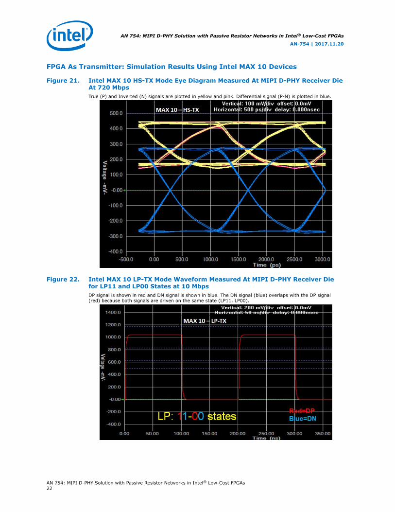
Figure 21. Intel MAX 10 HS-TX Mode Eye Diagram Measured At MIPI D-PHY Receiver DieAt 720 MbpsTrue (P) and Inverted (N) signals are plotted in yellow and pink. Differential signal (P-N) is plotted in blue.
Figure 22. Intel MAX 10 LP-TX Mode Waveform Measured At MIPI D-PHY Receiver Diefor LP11 and LP00 States at 10 MbpsDP signal is shown in red and DN signal is shown in blue. The DN signal (blue) overlaps with the DP signal(red) because both signals are driven on the same state (LP11, LP00).
AN 754: MIPI D-PHY Solution with Passive Resistor Networks in Intel® Low-Cost FPGAs
AN-754 | 2017.11.20
AN 754: MIPI D-PHY Solution with Passive Resistor Networks in Intel® Low-Cost FPGAs22

Figure 23. Intel MAX 10 LP-TX Mode Waveform Measured At MIPI D-PHY Receiver Diefor LP10 and LP01 States at 10 MbpsBoth DP and DN signals are not overlapped because they are driven out of phase (LP10, LP01).
PCB Design Guidelines
The interconnect between the MIPI TX and RX devices must be designed with caution.The interconnect includes PCB traces, connectors (if any), and cable media (typicallyflex-foils).
Signal quality guidelines are as follows:
• Match the electrical length of all pairs as close as possible to maximize data validmargins.
• Place the passive components as close as possible to the FPGA. Avoid any stubwhen placing the passive resistors on the high-speed signal trace. Minimize thestub length from the low-power signal trace to high-speed signal trace.
• Use the on chip termination feature on FPGA I/O whenever possible.
• The reference characteristics impedance level per line is 100 Ω for differential and50 Ω for single-ended. Control the impedance of the trace on the PCB to avoidimpedance mismatch between the driver output impedance and input impedanceof the receiver over the operating frequency.
• Keep the traces matched in lengths and as short as possible. The flight time forsignals across the interconnect should not exceed 2 ns.
• Ensure equal length for all high-speed differential traces. The differential channelis also used for low-power single-ended signaling. Intel recommends applying onlyvery loosely coupled differential transmission lines.
AN 754: MIPI D-PHY Solution with Passive Resistor Networks in Intel® Low-Cost FPGAs
AN-754 | 2017.11.20
AN 754: MIPI D-PHY Solution with Passive Resistor Networks in Intel® Low-Cost FPGAs23

• If probe points are required, ensure they are in line with the trace and notcreating a transmission line stub.
• Do not place noisy signals (example: voltage regulator module, clock generator)over or near MIPI signals.
• Use the I/O standards supported for the FPGA I/O as listed in the I/O standardsfor MIPI D-PHY Implementation table.
Related Links
• I/O Standards for MIPI D-PHY Implementation on page 6
• I/O Features in Cyclone IV Devices Chapter, Cyclone IV Device Handbook Volume1
Provides the I/O banks locations in Cyclone IV devices.
• I/O Features in Cyclone V Devices Chapter, Cyclone V Device Handbook Volume 1:Device Interfaces and Integration
Provides the I/O banks locations in Cyclone V Devices. All the I/O banks in theCyclone V devices can accommodate both the single-ended and differentialI/Os, except the HPS row and column I/O banks.
• MAX 10 I/O Banks Locations, MAX 10 General Purpose I/O User GuideProvides the I/O banks locations in MAX 10 devices.
• Support Resources: Board DesignProvides more information about the general board design guidelines.
Conclusion
The passive resistor network in this application illustrates and validates the IBISsimulations. You can use the passive resistor network to build a FPGA I/O basedcompatible MIPI D-PHY for receiving or transmitting both high-speed and low-powersignals using various FPGA GPIO connected. The passive resistor network is capable toenable an electrically compatible connection between Intel FPGA I/O to a MIPI D-PHYTX or RX device via MIPI D-PHY interface.
Table 11. Passive Resistor Values Used in the IBIS SimulationsRefer to the FPGA Unidirectional Receiver Implementation Block Diagram and FPGA Unidirectional TransmitterImplementation Block Diagram for the simulation block diagrams.
FPGA Implementation Passive Resistor Value (Ω)
Rx Ry xx yy zz
FPGA unidirectional receiver implementation 300 100 — — —
FPGA unidirectional transmitter implementation — — 150 60 100
Note: MIPI D-PHY solution can also use others I/O standards that are powered with differentVCCIO. This will be available in a future release of this application note.
Table 12. Maximum Achievable Data Rate Using Intel FPGA GPIOThe maximum achievable data rate depends on the device speed grade.
Device Supported Data Rate (Mbps)
Cyclone IV, Cyclone V 840
Intel MAX 10 720
AN 754: MIPI D-PHY Solution with Passive Resistor Networks in Intel® Low-Cost FPGAs
AN-754 | 2017.11.20
AN 754: MIPI D-PHY Solution with Passive Resistor Networks in Intel® Low-Cost FPGAs24

Intel recommends performing HSPICE/IBIS simulations to verify the signal qualitybased on your specific system setup and PCB info at the desired operating frequency.
Actual achievable frequency depends on design- and system-specific factors. PerformHSPICE/IBIS simulation based on your specific design, system setup, and PCB info todetermine the maximum achievable frequency.
The MIPI D-PHY passive solution with different approaches (I/O, passive network, andFPGA devices) are validated using multiple demo boards. You can use the followingdemo boards as reference:
• Intel 10M50 Evaluation Kit, EK-10M50F484 (available March 2016 onwards)
• Internal HSMC Passive D-PHY lab validation board for use with Cyclone VDevelopment Kits
• Arrow DECA Intel MAX 10 Evaluation Kit
For more information about the demo boards, contact your local Intel salesrepresentatives.
Related Links
I/O Standards for MIPI D-PHY Implementation on page 6
Document Revision History for AN 754: MIPI D-PHY Solution withPassive Resistor Networks in Intel Low-Cost FPGAs
Date Version Changes
November 2017 2017.11.20 Updated links.
May 2017 2017.05.08 Rebranded as Intel.
December 2015 2015.12.23 Initial release.
AN 754: MIPI D-PHY Solution with Passive Resistor Networks in Intel® Low-Cost FPGAs
AN-754 | 2017.11.20
AN 754: MIPI D-PHY Solution with Passive Resistor Networks in Intel® Low-Cost FPGAs25