250 mA, 16V, Low Quiescent Current LDO...
31
2012-2013 Microchip Technology Inc. DS20005122B-page 1 MCP1703A Features: • Reduced Ground Current During Dropout • Faster Startup Time • 2.0 μA Typical Quiescent Current • Input Operating Voltage Range: 2.7V to16.0V • 250 mA Output Current for Output Voltages ≥ 2.5V • 200 mA Output Current for Output Voltages < 2.5V • Low Dropout Voltage, 625 mV Typical @ 250 mA for V R = 2.8V • 0.4% Typical Output Voltage Tolerance • Standard Output Voltage Options: - 1.2V, 1.5V, 1.8V, 2.5V, 2.8V, 3.0V, 3.3V, 4.0V, 5.0V • Output Voltage Range: 1.2V to 5.5V in 0.1V Increments (50 mV increments available upon request) • A/D Friendly Voltage Options: 2.05V, 3.07V, 4.1V • Stable with 1.0 μF to 22 μF Ceramic Output Capacitance • Short-Circuit Protection • Overtemperature Protection Applications: • Battery-Powered Devices • Battery-Powered Alarm Circuits • Smoke Detectors • CO 2 Detectors • Pagers and Cellular Phones • Smart Battery Packs • Low Quiescent Current Voltage Reference • PDAs • Digital Cameras • Microcontroller Power • Solar-Powered Instruments • Consumer Products Related Literature: • AN765, “Using Microchip’s Micropower LDOs”, DS00765, Microchip Technology Inc., 2007 • AN766, “Pin-Compatible CMOS Upgrades to Bipolar LDOs”, DS00766, Microchip Technology Inc., 2003 • AN792, “A Method to Determine How Much Power a SOT23 Can Dissipate in an Application”, DS00792, Microchip Technology Inc., 2001 Description: The MCP1703A is an improved version of the MCP1703 low dropout (LDO) voltage regulator that can deliver up to 250 mA of current while consuming only 2.0 μA of quiescent current (typical). The input operating range is specified from 2.7V to 16.0V, making it an ideal choice for two to six primary cell battery- powered applications, 9V alkaline and one or two-cell Li-Ion-powered applications. The MCP1703A is capable of delivering 250 mA with only 625 mV (typical) of input to output voltage differential (V OUT = 2.8V). The output voltage tolerance of the MCP1703A is typically ±0.4% at +25°C and ±3% maximum over the operating junction temperature range of -40°C to +125°C. Line regulation is ±0.1% typical at +25°C. Output voltages available for the MCP1703A range from 1.2V to 5.5V. The LDO output is stable when using only 1 μF of output capacitance. Ceramic, tantalum or aluminum electrolytic capacitors can all be used for input and output. Overcurrent limit and overtemperature shutdown provide a robust solution for any application. Package options include the SOT-223-3, SOT-23A, 2x3 DFN-8 and SOT-89-3. Package Types 1 3 2 V IN GND V OUT 1 2 3 V IN GND V OUT SOT-23A SOT-89 V IN 1 2 3 SOT-223 GND V IN V OUT NC NC GND NC NC 1 2 3 4 8 7 6 5 NC V OUT EP 9 * Includes Exposed Thermal Pad (EP); see Table 3-1. V IN 2x3 DFN* 250 mA, 16V, Low Quiescent Current LDO Regulator
Transcript of 250 mA, 16V, Low Quiescent Current LDO...

MCP1703A250 mA, 16V, Low Quiescent Current LDO Regulator
Features:
• Reduced Ground Current During Dropout
• Faster Startup Time
• 2.0 µA Typical Quiescent Current
• Input Operating Voltage Range: 2.7V to16.0V
• 250 mA Output Current for Output Voltages ≥ 2.5V
• 200 mA Output Current for Output Voltages < 2.5V
• Low Dropout Voltage, 625 mV Typical @ 250 mA for VR = 2.8V
• 0.4% Typical Output Voltage Tolerance
• Standard Output Voltage Options:
- 1.2V, 1.5V, 1.8V, 2.5V, 2.8V, 3.0V, 3.3V, 4.0V, 5.0V
• Output Voltage Range: 1.2V to 5.5V in 0.1V Increments (50 mV increments available upon request)
• A/D Friendly Voltage Options: 2.05V, 3.07V, 4.1V
• Stable with 1.0 µF to 22 µF Ceramic Output Capacitance
• Short-Circuit Protection
• Overtemperature Protection
Applications:
• Battery-Powered Devices
• Battery-Powered Alarm Circuits
• Smoke Detectors
• CO2 Detectors
• Pagers and Cellular Phones
• Smart Battery Packs
• Low Quiescent Current Voltage Reference
• PDAs
• Digital Cameras
• Microcontroller Power
• Solar-Powered Instruments
• Consumer Products
Related Literature:
• AN765, “Using Microchip’s Micropower LDOs”, DS00765, Microchip Technology Inc., 2007
• AN766, “Pin-Compatible CMOS Upgrades to Bipolar LDOs”, DS00766, Microchip Technology Inc., 2003
• AN792, “A Method to Determine How Much Power a SOT23 Can Dissipate in an Application”, DS00792, Microchip Technology Inc., 2001
Description:
The MCP1703A is an improved version of theMCP1703 low dropout (LDO) voltage regulator that candeliver up to 250 mA of current while consuming only2.0 µA of quiescent current (typical). The inputoperating range is specified from 2.7V to 16.0V, makingit an ideal choice for two to six primary cell battery-powered applications, 9V alkaline and one or two-cellLi-Ion-powered applications.
The MCP1703A is capable of delivering 250 mA withonly 625 mV (typical) of input to output voltagedifferential (VOUT = 2.8V). The output voltage toleranceof the MCP1703A is typically ±0.4% at +25°C and ±3%maximum over the operating junction temperaturerange of -40°C to +125°C. Line regulation is ±0.1%typical at +25°C.
Output voltages available for the MCP1703A rangefrom 1.2V to 5.5V. The LDO output is stable when usingonly 1 µF of output capacitance. Ceramic, tantalum oraluminum electrolytic capacitors can all be used forinput and output. Overcurrent limit and overtemperatureshutdown provide a robust solution for any application.Package options include the SOT-223-3, SOT-23A,2x3 DFN-8 and SOT-89-3.
Package Types
1
3
2
VIN
GND VOUT
1 2 3
VINGND VOUT
SOT-23A
SOT-89VIN
1 2 3
SOT-223
GNDVIN VOUT
NC
NC
GND
NC
NC
1
2
3
4
8
7
6
5 NC
VOUT
EP9
* Includes Exposed Thermal Pad (EP); see Table 3-1.
VIN
2x3 DFN*
2012-2013 Microchip Technology Inc. DS20005122B-page 1

MCP1703A
Functional Block Diagrams
Typical Application Circuits
+-
VIN VOUT
GND
+VIN
Error Amplifier
VoltageReference
OvercurrentOvertemperature
MCP1703A
VIN
CIN1 µF Ceramic
COUT1 µF Ceramic
VOUT
VIN
3.3V
IOUT50 mA
VIN
VOUT
9VBattery
+
GND
MCP1703A
DS20005122B-page 2 2012-2013 Microchip Technology Inc.

MCP1703A
1.0 ELECTRICAL CHARACTERISTICS
Absolute Maximum Ratings †
VDD..................................................................................+18V
All inputs and outputs w.r.t. .............(VSS-0.3V) to (VIN+0.3V)
Peak Output Current ...................................................500 mA
Storage temperature .....................................-65°C to +150°C
Maximum Junction Temperature................................. +150°C
ESD protection on all pins (HBM; MM) ............. ≥ 4 kV; ≥ 400V
† Notice: Stresses above those listed under “MaximumRatings” may cause permanent damage to the device. This isa stress rating only and functional operation of the device atthose or any other conditions above those indicated in theoperational listings of this specification is not implied.Exposure to maximum rating conditions for extended periodsmay affect device reliability.
DC CHARACTERISTICSElectrical Specifications: Unless otherwise specified, all limits are established for VIN = VOUT(MAX) + VDROPOUT(MAX), Note 1, ILOAD = 1 mA, COUT = 1 µF (X7R), CIN = 1 µF (X7R), TA = +25°C. Boldface type applies for junction temperatures, TJ (Note 7) of -40°C to +125°C.
Parameters Symbol Min Typ Max Units Conditions
Input / Output Characteristics
Input Operating Voltage VIN 2.7 — 16.0 V Note 1
Input Quiescent Current Iq — 2.0 5 µA IL = 0 mA
Maximum Output Current IOUT 250 — — mA For VR ≥ 2.5V
50 100 — mA For VR < 2.5V, VIN ≥ 2.7V
100 130 — mA For VR < 2.5V, VIN ≥ 2.95V
150 200 — mA For VR < 2.5V, VIN ≥ 3.2V
200 230 — mA For VR < 2.5V, VIN ≥ 3.45V
Output Short Circuit Current IOUT_SC — 400 — mA VIN = VIN(MIN) (Note 1), VOUT = GND,Current (average current) measured 10 ms after short is applied.
Output Voltage Regulation VOUT VR-3.0% VR±0.4% VR+3.0% V Note 2
VR-2.0% VR±0.4% VR+2.0% V
VR-1.0% VR±0.4% VR+1.0% V 1% Custom
VOUT Temperature Coefficient TCVOUT — 65 — ppm/°C Note 3
Line Regulation DVOUT/(VOUTxΔVIN)
-0.3 ±0.1 +0.3 %/V (VOUT(MAX) + VDROPOUT(MAX)) ≤ VIN ≤ 16V, Note 1
Load Regulation ΔVOUT/VOUT -2.5 ±1.0 +2.5 % IL = 1.0 mA to 250 mA for VR ≥ 2.5VIL = 1.0 mA to 200 mA for VR < 2.5VVIN = 3.65V, Note 4
Note 1: The minimum VIN must meet two conditions: VIN ≥ 2.7V and VIN ≥ (VOUT(MAX) + VDROPOUT(MAX)).2: VR is the nominal regulator output voltage. For example: VR = 1.2V, 1.5V, 1.8V, 2.5V, 2.8V, 3.0V, 3.3V, 4.0V or 5.0V. The
input voltage VIN = VOUT(MAX) + VDROPOUT(MAX) or ViIN = 2.7V (whichever is greater); IOUT = 100 µA.3: TCVOUT = (VOUT-HIGH - VOUT-LOW) x 106/(VR x ΔTemperature), VOUT-HIGH = highest voltage measured over the
temperature range. VOUT-LOW = lowest voltage measured over the temperature range.4: Load regulation is measured at a constant junction temperature using low duty cycle pulse testing. Changes in output
voltage due to heating effects are determined using thermal regulation specification TCVOUT.5: Dropout voltage is defined as the input to output differential at which the output voltage drops 2% below its measured
value with an applied input voltage of VOUT(MAX) + VDROPOUT(MAX) or 2.7V, whichever is greater.6: The maximum allowable power dissipation is a function of ambient temperature, the maximum allowable junction
temperature and the thermal resistance from junction to air (i.e., TA, TJ, qJA). Exceeding the maximum allowable power dissipation will cause the device operating junction temperature to exceed the maximum 150°C rating. Sustained junction temperatures above 150°C can impact the device reliability.
7: The junction temperature is approximated by soaking the device under test at an ambient temperature equal to the desired junction temperature. The test time is small enough such that the rise in the junction temperature over the ambient temperature is not significant.
2012-2013 Microchip Technology Inc. DS20005122B-page 3
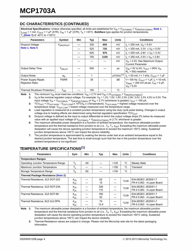
MCP1703A
Dropout VoltageNote 1, Note 5
VDROPOUT — 330 650 mV IL = 250 mA, VR = 5.0V
— 525 725 mV IL = 250 mA, 3.3V ≤ VR < 5.0V
— 625 975 mV IL = 250 mA, 2.8V ≤ VR < 3.3V
— 750 1100 mV IL = 250 mA, 2.5V ≤ VR < 2.8V
— — — mV VR < 2.5V, See Maximum Output Current Parameter
Output Delay Time TDELAY — 600 — µs VIN = 0V to 6V, VOUT = 90% VR,RL = 50Ω resistive
Output Noise eN — 1 µV/(Hz)1/2 IL = 50 mA, f = 1 kHz, COUT = 1 µF
Power Supply Ripple Rejection Ratio
PSRR — 35 — dB f = 100 Hz, COUT = 1 µF, IL = 10 mA, VINAC = 200 mV pk-pk, CIN = 0 µF, VR = 5.0V
Thermal Shutdown Protection TSD — 150 — °C
TEMPERATURE SPECIFICATIONS(1)
Parameters Sym Min Typ Max Units Conditions
Temperature Ranges
Operating Junction Temperature Range TJ -40 — +125 °C Steady State
Maximum Junction Temperature TJ — — +150 °C Transient
Storage Temperature Range TA -65 — +150 °C
Thermal Package Resistance (Note 2)
Thermal Resistance, 3LD SOT-223 θJAθJC
——
6215
——
°C/WEIA/JEDEC JESD51-7FR-4 0.063 4-Layer Board
Thermal Resistance, 3LD SOT-23A θJAθJC
——
336110
——
°C/WEIA/JEDEC JESD51-7FR-4 0.063 4-Layer Board
Thermal Resistance, 3LD SOT-89 θJAθJC
——
18052
——
°C/WEIA/JEDEC JESD51-7FR-4 0.063 4-Layer Board
Thermal Resistance, 8LD 2x3 DFN θJAθJC
——
7013.4
——
°C/WEIA/JEDEC JESD51-7FR-4 0.063 4-Layer Board
Note 1: The maximum allowable power dissipation is a function of ambient temperature, the maximum allowable junction temperature and the thermal resistance from junction to air (i.e., TA, TJ, θJA). Exceeding the maximum allowable power dissipation will cause the device operating junction temperature to exceed the maximum 150°C rating. Sustained junction temperatures above 150°C can impact the device reliability.
2: Thermal Resistance values are subject to change. Please visit the Microchip web site for the latest packaging information.
DC CHARACTERISTICS (CONTINUED)Electrical Specifications: Unless otherwise specified, all limits are established for VIN = VOUT(MAX) + VDROPOUT(MAX), Note 1, ILOAD = 1 mA, COUT = 1 µF (X7R), CIN = 1 µF (X7R), TA = +25°C. Boldface type applies for junction temperatures, TJ (Note 7) of -40°C to +125°C.
Parameters Symbol Min Typ Max Units Conditions
Note 1: The minimum VIN must meet two conditions: VIN ≥ 2.7V and VIN ≥ (VOUT(MAX) + VDROPOUT(MAX)).2: VR is the nominal regulator output voltage. For example: VR = 1.2V, 1.5V, 1.8V, 2.5V, 2.8V, 3.0V, 3.3V, 4.0V or 5.0V. The
input voltage VIN = VOUT(MAX) + VDROPOUT(MAX) or ViIN = 2.7V (whichever is greater); IOUT = 100 µA.3: TCVOUT = (VOUT-HIGH - VOUT-LOW) x 106/(VR x ΔTemperature), VOUT-HIGH = highest voltage measured over the
temperature range. VOUT-LOW = lowest voltage measured over the temperature range.4: Load regulation is measured at a constant junction temperature using low duty cycle pulse testing. Changes in output
voltage due to heating effects are determined using thermal regulation specification TCVOUT.5: Dropout voltage is defined as the input to output differential at which the output voltage drops 2% below its measured
value with an applied input voltage of VOUT(MAX) + VDROPOUT(MAX) or 2.7V, whichever is greater.6: The maximum allowable power dissipation is a function of ambient temperature, the maximum allowable junction
temperature and the thermal resistance from junction to air (i.e., TA, TJ, qJA). Exceeding the maximum allowable power dissipation will cause the device operating junction temperature to exceed the maximum 150°C rating. Sustained junction temperatures above 150°C can impact the device reliability.
7: The junction temperature is approximated by soaking the device under test at an ambient temperature equal to the desired junction temperature. The test time is small enough such that the rise in the junction temperature over the ambient temperature is not significant.
DS20005122B-page 4 2012-2013 Microchip Technology Inc.
MCP1703A
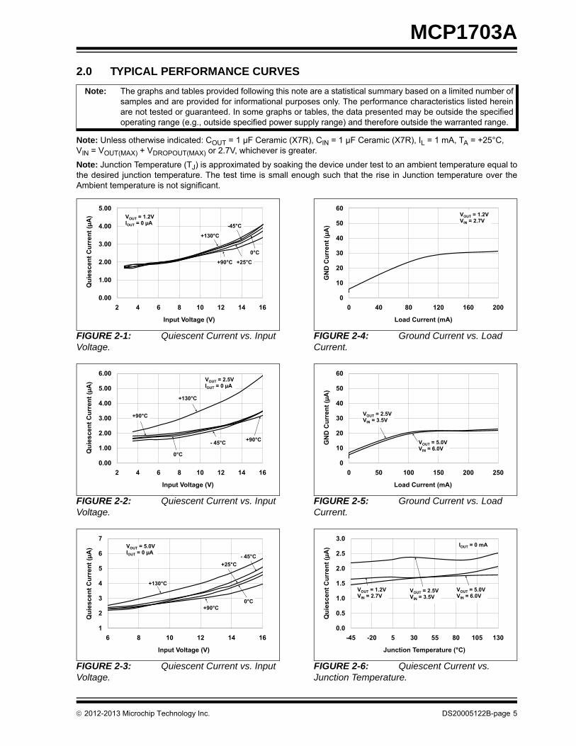
2.0 TYPICAL PERFORMANCE CURVES
Note: Unless otherwise indicated: COUT = 1 µF Ceramic (X7R), CIN = 1 µF Ceramic (X7R), IL = 1 mA, TA = +25°C, VIN = VOUT(MAX) + VDROPOUT(MAX) or 2.7V, whichever is greater.
Note: Junction Temperature (TJ) is approximated by soaking the device under test to an ambient temperature equal tothe desired junction temperature. The test time is small enough such that the rise in Junction temperature over theAmbient temperature is not significant.
FIGURE 2-1: Quiescent Current vs. Input Voltage.
FIGURE 2-2: Quiescent Current vs. Input Voltage.
FIGURE 2-3: Quiescent Current vs. Input Voltage.
FIGURE 2-4: Ground Current vs. Load Current.
FIGURE 2-5: Ground Current vs. Load Current.
FIGURE 2-6: Quiescent Current vs. Junction Temperature.
Note: The graphs and tables provided following this note are a statistical summary based on a limited number ofsamples and are provided for informational purposes only. The performance characteristics listed hereinare not tested or guaranteed. In some graphs or tables, the data presented may be outside the specifiedoperating range (e.g., outside specified power supply range) and therefore outside the warranted range.
0.00
1.00
2.00
3.00
4.00
5.00
2 4 6 8 10 12 14 16
Qui
esce
nt C
urre
nt (µ
A)
Input Voltage (V)
VOUT = 1.2VIOUT = 0 µA
+25°C
+130°C
-45°C
0°C
+90°C
0.00
1.00
2.00
3.00
4.00
5.00
6.00
2 4 6 8 10 12 14 16
Qui
esce
nt C
urre
nt (µ
A)
Input Voltage (V)
VOUT = 2.5VIOUT = 0 µA
+90°C
+130°C
- 45°C
0°C
+90°C
1
2
3
4
5
6
7
6 8 10 12 14 16
Qui
esce
nt C
urre
nt (µ
A)
Input Voltage (V)
VOUT = 5.0VIOUT = 0 µA
0°C
+130°C
- 45°C+25°C
+90°C
0
10
20
30
40
50
60
0 40 80 120 160 200
GN
D C
urre
nt (µ
A)
Load Current (mA)
VOUT = 1.2VVIN = 2.7V
0
10
20
30
40
50
60
0 50 100 150 200 250
GN
D C
urre
nt (µ
A)
Load Current (mA)
VOUT = 2.5VVIN = 3.5V
VOUT = 5.0VVIN = 6.0V
0.0
0.5
1.0
1.5
2.0
2.5
3.0
-45 -20 5 30 55 80 105 130
Qui
esce
nt C
urre
nt (µ
A)
Junction Temperature (°C)
IOUT = 0 mA
VOUT = 5.0VVIN = 6.0V
VOUT = 1.2VVIN = 2.7V
VOUT = 2.5VVIN = 3.5V
2012-2013 Microchip Technology Inc. DS20005122B-page 5
MCP1703A
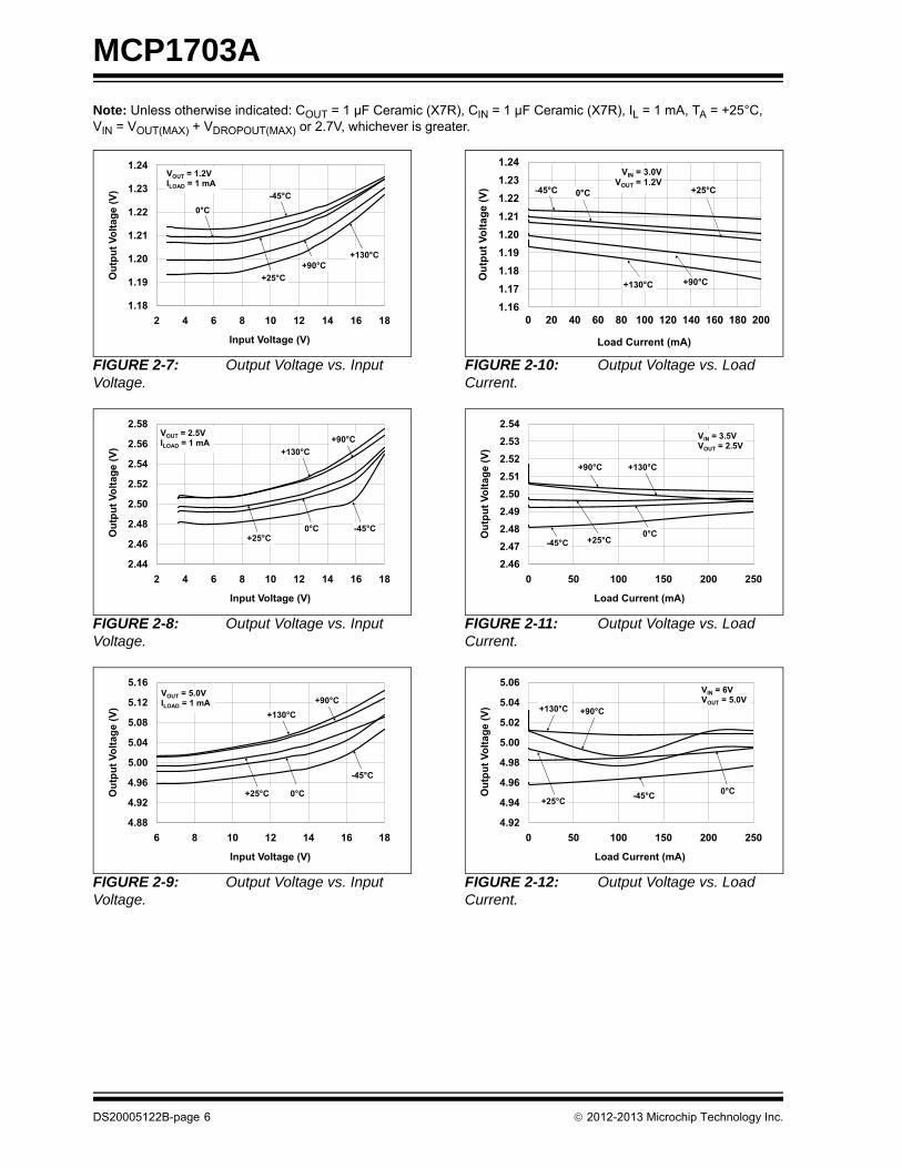
Note: Unless otherwise indicated: COUT = 1 µF Ceramic (X7R), CIN = 1 µF Ceramic (X7R), IL = 1 mA, TA = +25°C, VIN = VOUT(MAX) + VDROPOUT(MAX) or 2.7V, whichever is greater.
FIGURE 2-7: Output Voltage vs. Input Voltage.
FIGURE 2-8: Output Voltage vs. Input Voltage.
FIGURE 2-9: Output Voltage vs. Input Voltage.
FIGURE 2-10: Output Voltage vs. Load Current.
FIGURE 2-11: Output Voltage vs. Load Current.
FIGURE 2-12: Output Voltage vs. Load Current.
1.18
1.19
1.20
1.21
1.22
1.23
1.24
2 4 6 8 10 12 14 16 18
Out
put V
olta
ge (V
)
Input Voltage (V)
VOUT = 1.2VILOAD = 1 mA
+25°C
+130°C
-45°C0°C
+90°C
2.44
2.46
2.48
2.50
2.52
2.54
2.56
2.58
2 4 6 8 10 12 14 16 18
Out
put V
olta
ge (V
)
Input Voltage (V)
VOUT = 2.5VILOAD = 1 mA
+25°C
+130°C
-45°C0°C
+90°C
4.88
4.92
4.96
5.00
5.04
5.08
5.12
5.16
6 8 10 12 14 16 18
Out
put V
olta
ge (V
)
Input Voltage (V)
VOUT = 5.0VILOAD = 1 mA
+25°C
+130°C
-45°C
0°C
+90°C
1.161.171.181.191.201.211.221.231.24
0 20 40 60 80 100 120 140 160 180 200
Out
put V
olta
ge (V
)
Load Current (mA)
VIN = 3.0VVOUT = 1.2V
+25°C
+130°C
-45°C 0°C
+90°C
2.462.472.482.492.502.512.522.532.54
0 50 100 150 200 250
Out
put V
olta
ge (V
)
Load Current (mA)
VIN = 3.5VVOUT = 2.5V
+25°C
+130°C
-45°C0°C
+90°C
4.92
4.94
4.96
4.98
5.00
5.02
5.04
5.06
0 50 100 150 200 250
Out
put V
olta
ge (V
)
Load Current (mA)
VIN = 6VVOUT = 5.0V
+25°C
+130°C
-45°C 0°C
+90°C
DS20005122B-page 6 2012-2013 Microchip Technology Inc.
MCP1703A
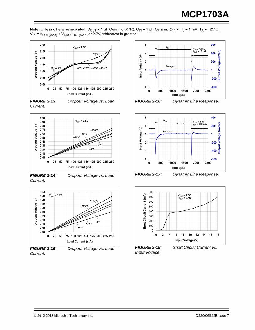
Note: Unless otherwise indicated: COUT = 1 µF Ceramic (X7R), CIN = 1 µF Ceramic (X7R), IL = 1 mA, TA = +25°C, VIN = VOUT(MAX) + VDROPOUT(MAX) or 2.7V, whichever is greater.
FIGURE 2-13: Dropout Voltage vs. Load Current.
FIGURE 2-14: Dropout Voltage vs. Load Current.
FIGURE 2-15: Dropout Voltage vs. Load Current.
FIGURE 2-16: Dynamic Line Response.
FIGURE 2-17: Dynamic Line Response.
FIGURE 2-18: Short Circuit Current vs. Input Voltage.
0.00
0.50
1.00
1.50
2.00
2.50
3.00
0 25 50 75 100 125 150 175 200 225 250
Dro
pout
Vol
tage
(V)
Load Current (mA)
VOUT = 1.2V
0°C, +25°C, +90°C, +130°C
- 45°C
- 45°C, 0°C
0.000.100.200.300.400.500.600.700.800.901.00
0 25 50 75 100 125 150 175 200 225 250
Dro
pout
Vol
tage
(V)
Load Current (mA)
VOUT = 2.5V
+25°C
+130°C
0°C- 45°C
+90°C
0.000.050.100.150.200.250.300.350.400.450.50
0 25 50 75 100 125 150 175 200 225 250
Dro
pout
Vol
tage
(V)
Load Current (mA)
VOUT = 5.0V
+25°C
+130°C
0°C
- 45°C
+90°C
0
200
400
600
2
3
4
5
put V
olta
ge (m
Vac)
nput
Vol
tage
(V)
VOUT = 2.5VIOUT = 10 mA
VIN
VOUT(AC)
-400
-200
0
1
0 500 1000 1500 2000 2500
Out
pIn
Time (µs)
-200
0
200
400
2
3
4
5
put V
olta
ge (m
Vac)
nput
Vol
tage
(V)
VOUT = 2.5VIOUT = 100 mA
VIN
VOUT(AC)
-600
-400
0
1
0 500 1000 1500 2000 2500
OutIn
Time (µs)
0100200300400500600700800
0 2 4 6 8 10 12 14 16 18
Shor
t Circ
uit C
urre
nt (m
A)
Input Voltage (V)
VOUT = 2.5VROUT < 0.1Ω
2012-2013 Microchip Technology Inc. DS20005122B-page 7
MCP1703A
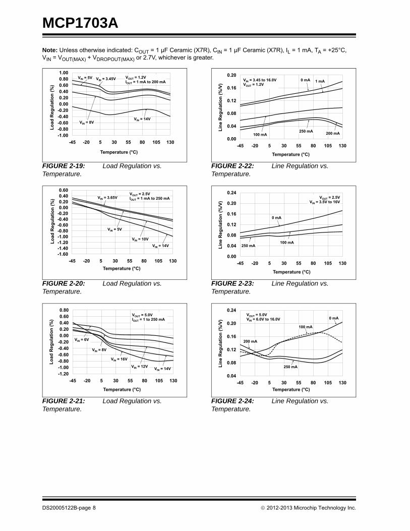
Note: Unless otherwise indicated: COUT = 1 µF Ceramic (X7R), CIN = 1 µF Ceramic (X7R), IL = 1 mA, TA = +25°C, VIN = VOUT(MAX) + VDROPOUT(MAX) or 2.7V, whichever is greater.
FIGURE 2-19: Load Regulation vs. Temperature.
FIGURE 2-20: Load Regulation vs. Temperature.
FIGURE 2-21: Load Regulation vs. Temperature.
FIGURE 2-22: Line Regulation vs. Temperature.
FIGURE 2-23: Line Regulation vs. Temperature.
FIGURE 2-24: Line Regulation vs. Temperature.
-1.00-0.80-0.60-0.40-0.200.000.200.400.600.801.00
-45 -20 5 30 55 80 105 130
Load
Reg
ulat
ion
(%)
Temperature (°C)
VOUT = 1.2VIOUT = 1 mA to 200 mA
VIN = 8VVIN = 14V
VIN = 3.45VVIN = 5V
-1.60-1.40-1.20-1.00-0.80-0.60-0.40-0.200.000.200.400.60
-45 -20 5 30 55 80 105 130
Load
Reg
ulat
ion
(%)
Temperature (°C)
VOUT = 2.5VIOUT = 1 mA to 250 mA
VIN = 5V
VIN = 14VVIN = 10V
VIN = 3.65V
-1.20-1.00-0.80-0.60-0.40-0.200.000.200.400.600.80
-45 -20 5 30 55 80 105 130
Load
Reg
ulat
ion
(%)
Temperature (°C)
VOUT = 5.0VIOUT = 1 to 250 mA
VIN = 6V
VIN = 14VVIN = 12V
VIN = 8V
VIN = 16V
0.00
0.04
0.08
0.12
0.16
0.20
-45 -20 5 30 55 80 105 130
Line
Reg
ulat
ion
(%/V
)
Temperature (°C)
VIN = 3.45 to 16.0VVOUT = 1.2V
1 mA
100 mA
0 mA
200 mA250 mA
0.00
0.04
0.08
0.12
0.16
0.20
0.24
-45 -20 5 30 55 80 105 130
Line
Reg
ulat
ion
(%/V
)
Temperature (°C)
VOUT = 2.5VVIN = 3.5V to 16V
100 mA
0 mA
250 mA
0.04
0.08
0.12
0.16
0.20
0.24
-45 -20 5 30 55 80 105 130
Line
Reg
ulat
ion
(%/V
)
Temperature (°C)
VOUT = 5.0VVIN = 6.0V to 16.0V
200 mA
100 mA
0 mA
250 mA
DS20005122B-page 8 2012-2013 Microchip Technology Inc.
MCP1703A
Note: Unless otherwise indicated: COUT = 1 µF Ceramic (X7R), CIN = 1 µF Ceramic (X7R), IL = 1 mA, TA = +25°C, VIN = VOUT(MAX) + VDROPOUT(MAX) or 2.7V, whichever is greater.
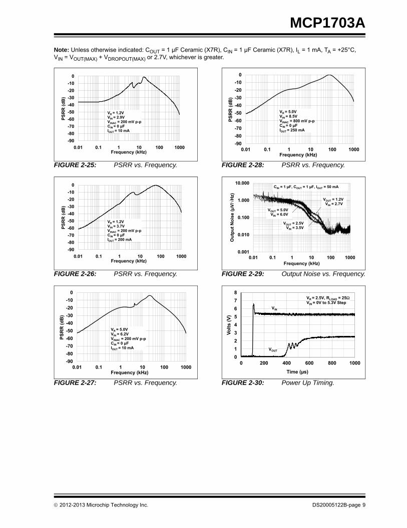
FIGURE 2-25: PSRR vs. Frequency.
FIGURE 2-26: PSRR vs. Frequency.
FIGURE 2-27: PSRR vs. Frequency.
FIGURE 2-28: PSRR vs. Frequency.
FIGURE 2-29: Output Noise vs. Frequency.
FIGURE 2-30: Power Up Timing.
-90-80-70-60-50-40-30-20-10
0
0.01 0.1 1 10 100 1000
PSR
R (d
B)
Frequency (kHz)
VR = 1.2VVIN = 2.9VVINAC = 200 mV p-pCIN = 0 μFIOUT = 10 mA
-90-80-70-60-50-40-30-20-10
0
0.01 0.1 1 10 100 1000
PSR
R (d
B)
Frequency (kHz)
VR = 1.2VVIN = 3.7VVINAC = 200 mV p-pCIN = 0 μFIOUT = 200 mA
-60-50-40-30-20-10
0
PSR
R (d
B)
VR = 5.0VVIN = 6.2VVINAC = 200 mV p-pC 0 F
-90-80-70
0.01 0.1 1 10 100 1000Frequency (kHz)
CIN = 0 FIOUT = 10 mA
-60-50-40-30-20-10
0
PSR
R (d
B)
VR = 5.0VVIN = 8.5VVINAC = 800 mV p-pC 0 F
-90-80-70
0.01 0.1 1 10 100 1000Frequency (kHz)
CIN = 0 FIOUT = 250 mA
0.100
1.000
10.000
ut N
oise
(μV/
Hz)
CIN = 1 μF, COUT = 1 μF, IOUT = 50 mA
VOUT = 2.5VVIN = 3.5V
VOUT = 5.0VVIN = 6.0V
VOUT = 1.2VVIN = 2.7V
0.001
0.010
0.01 0.1 1 10 100 1000
Out
p
Frequency (kHz)
012345678
0 200 400 600 800 1000
Volts
(V)
Time (µs)
VR = 2.5V, RLOAD = 25ΩVIN = 0V to 5.3V Step
VIN
VOUT
2012-2013 Microchip Technology Inc. DS20005122B-page 9

MCP1703A
Note: Unless otherwise indicated: COUT = 1 µF Ceramic (X7R), CIN = 1 µF Ceramic (X7R), IL = 1 mA, TA = +25°C, VIN = VOUT(MAX) + VDROPOUT(MAX) or 2.7V, whichever is greater.
FIGURE 2-31: Dynamic Load Response.
FIGURE 2-32: Dynamic Load Response.
FIGURE 2-33: Ground Current vs. Input Voltage.
FIGURE 2-34: Ground Current vs. Input Voltage.
FIGURE 2-35: Output Voltage vs. Input Voltage.
FIGURE 2-36: Dropout Current vs. Input Voltage.
0
5
10
15
20
25
30
-1500
-1000
-500
0
500
1000
1500
0 500 1000 1500 2000 2500
Out
put V
olta
ge (m
V)
Time (µs)
VOUT = 2.5VStep 100µ to 100 mA
100 mA
100 µA
VOUT (ac)
0
5
10
15
20
25
30
-1500
-1000
-500
0
500
1000
1500
0 500 1000 1500 2000 2500
Out
put V
olta
ge (m
V)
Time (µs)
VOUT = 2.5VStep 1 mA to 200 mA
1 mA
200 mA
VOUT (ac)
0
4
8
12
16
20
024681012141618
Gro
und
Cur
rent
(µA
)
Input Voltage (V)
VOUT = 2.5VIOUT = 10 mA
0
4
8
12
16
20
024681012141618
Gro
und
Cur
rent
(µA
)
Input Voltage (V)
VOUT = 5.0VIOUT = 10 mA
0
1
2
3
4
5
6
0123456
Out
put V
olta
ge (V
)
Input Voltage (V)
IOUT = 1 mAVOUT = 5V
VOUT = 3.3V
0
2
4
6
8
10
0123456
Dro
pout
Cur
rent
(µA
)
Input Voltage (V)
IOUT = 1 mAVOUT = 5V
VOUT = 3.3V
DS20005122B-page 10 2012-2013 Microchip Technology Inc.

MCP1703A
3.0 PIN DESCRIPTIONS
The descriptions of the pins are listed in Table 3-1.
3.1 Ground Terminal (GND)
Regulator ground. Tie GND to the negative side of theoutput and the negative side of the input capacitor.There is no high current and only the LDO bias current(2.0 µA typical) flows out of this pin. The LDO outputregulation is referenced to this pin. Minimize voltagedrops between this pin and the negative side of theload.
3.2 Regulated Output Voltage (VOUT)
Connect VOUT to the positive side of the load and thepositive terminal of the output capacitor. The positiveside of the output capacitor should be physicallylocated close to the LDO VOUT pin as is practical. Thecurrent flowing out of this pin is equal to the DC loadcurrent.
3.3 Unregulated Input Voltage (VIN)
Connect VIN to the input unregulated source voltage.Like all low dropout linear regulators, low sourceimpedance is necessary for stable operation of theLDO. The amount of capacitance required to ensurelow source impedance depends on the proximity of theinput source capacitors or battery type. For mostapplications, 1 µF of capacitance ensures stableoperation of the LDO circuit. The input capacitancerequirement can be lowered for applications that haveload currents below 100 mA. The type of capacitorused can be ceramic, tantalum or aluminumelectrolytic. The low ESR characteristics of the ceramicyields better noise and PSRR performance athigh-frequency.
3.4 Exposed Thermal Pad (EP)
An internal electrical connection between the ExposedThermal Pad (EP) and the VSS pin. They must beconnected to the same potential on the Printed CircuitBoard (PCB).
TABLE 3-1: MCP1703A PIN FUNCTION TABLE
2x3 DFN SOT-223 SOT-23A SOT-89 Name Function
4 2,Tab 1 1 GND Ground Terminal
1 3 2 3 VOUT Regulated Voltage Output
8 1 3 2,Tab VIN Unregulated Supply Voltage
2, 3, 5, 6, 7 — — — NC No Connection
9 — — — EP Exposed Thermal Pad (EP); must be connected to VSS
2012-2013 Microchip Technology Inc. DS20005122B-page 11

MCP1703A
4.0 DETAILED DESCRIPTION
4.1 Output Regulation
A portion of the LDO output voltage is fed back to theinternal error amplifier and compared with the precisioninternal band gap reference. The error amplifier outputadjusts the amount of current that flows through the P-Channel pass transistor, thus regulating the outputvoltage to the desired value. Any changes in inputvoltage or output current causes the error amplifier torespond and adjust the output voltage to the targetvoltage (see Figure 4-1).
4.2 Overcurrent
The MCP1703A internal circuitry monitors the amountof current flowing through the P-Channel passtransistor. In the event of a short-circuit or excessiveoutput current, the MCP1703A turns off the P-Channeldevice for a short period, after which the LDO attemptsto restart. If the excessive current remains, the cyclewill repeat itself.
4.3 Overtemperature
The internal power dissipation within the LDO is afunction of input-to-output voltage differential and loadcurrent. If the power dissipation within the LDO isexcessive, the internal junction temperature risesabove the typical shutdown threshold of 150°C. At thatpoint, the LDO shuts down and begins to cool to thetypical turn-on junction temperature of 130°C. If thepower dissipation is low enough, the device willcontinue to cool and operate normally. If the powerdissipation remains high, the thermal shutdownprotection circuitry will again turn off the LDO,protecting it from catastrophic failure.
FIGURE 4-1: Block Diagram.
+-
VIN VOUT
GND
+VIN
Error Amplifier
VoltageReference
OvercurrentOvertemperature
MCP1703A
DS20005122B-page 12 2012-2013 Microchip Technology Inc.

MCP1703A
5.0 FUNCTIONAL DESCRIPTION
The MCP1703A CMOS low dropout linear regulator isintended for applications that need the lowest currentconsumption while maintaining output voltageregulation. The operating continuous load range of theMCP1703A is from 0 mA to 250 mA (VR ≥ 2.5V). Theinput operating voltage ranges from 2.7V to 16.0V,making it capable of operating from two or morealkaline cells or single and multiple Li-Ion cell batteries.
5.1 Input
The input of the MCP1703A is connected to the sourceof the P-Channel PMOS pass transistor. As with allLDO circuits, a relatively low source impedance (10Ω)is needed to prevent the input impedance from causingthe LDO to become unstable. The size and type of thecapacitor needed depends heavily on the input sourcetype (e.g., battery, power supply) and the output currentrange of the application. To ensure circuit stability, a1 µF ceramic capacitor is sufficient for mostapplications up to 100 mA. Larger values can be usedto improve circuit AC performance. The capacitance ofthe input capacitor should be equal to or greater thanthe capacitance of the selected output capacitor toensure energy is available to keep the output capacitorcharged during dynamic load changes.
5.2 Output
The maximum rated continuous output current for theMCP1703A is 250 mA (VR ≥ 2.5V). For applicationswhere VR < 2.5V, the maximum output current is200 mA.
A minimum output capacitance of 1.0 µF is required forsmall signal stability in applications that have up to250 mA output current capability. The capacitor typecan be ceramic, tantalum or aluminum electrolytic. TheEquivalent Series Resistance (ESR) range on theoutput capacitor ranges from 0Ω to 2.0Ω.
The output capacitor range for ceramic capacitors is1 µF to 22 µF. Higher output capacitance values maybe used for tantalum and electrolytic capacitors. Higheroutput capacitor values pull the pole of the LDOtransfer function inward that results in higher phaseshifts which in turn cause a lower crossover frequency.The circuit designer should verify the stability byapplying line step and load step testing to their systemwhen using capacitance values greater than 22 µF.
5.3 Output Rise Time
When powering up the internal reference output, thetypical output rise time of 600 µs is controlled toprevent overshoot of the output voltage.
2012-2013 Microchip Technology Inc. DS20005122B-page 13

MCP1703A
6.0 APPLICATION CIRCUITS AND ISSUES
6.1 Typical Application
The MCP1703A is most commonly used as a voltageregulator. Its low quiescent current and low dropoutvoltage make it ideal for many battery-poweredapplications.
FIGURE 6-1: Typical Application Circuit.
6.1.1 APPLICATION INPUT CONDITIONS
6.2 Power Calculations
6.2.1 POWER DISSIPATION
The internal power dissipation of the MCP1703A is afunction of input voltage, output voltage and outputcurrent. As a result of the quiescent current draw, thepower dissipation is so low that it is insignificant (2.0 µAx VIN). The following equation can be used to calculatethe internal power dissipation of the LDO.
EQUATION 6-1:
The maximum continuous operating junctiontemperature specified for the MCP1703A is +125°C. Toestimate the internal junction temperature of theMCP1703A, the total internal power dissipation ismultiplied by the thermal resistance from junction toambient (RθJA). The thermal resistance from junctionto ambient for the SOT-23A pin package is estimated at336°C/W.
EQUATION 6-2:
The maximum power dissipation capability for apackage can be calculated given the junction-to-ambient thermal resistance and the maximum ambienttemperature for the application. The following equationcan be used to determine the package maximuminternal power dissipation.
EQUATION 6-3:
EQUATION 6-4:
EQUATION 6-5:
Package Type = SOT-23A
Input Voltage Range = 2.7V to 4.8V
VIN maximum = 4.8V
VOUT typical = 1.8V
IOUT = 50 mA maximum
GND
VOUT
VINCIN1 µF Ceramic
COUT1 µF Ceramic
VOUT
VIN2.7V to 4.8V
1.8V
IOUT50 mA
MCP1703A
PLDO VIN MAX( ) VOUT MIN( )–( ) IOUT MAX( )×=
Where:
PLDO = LDO Pass device internal power dissipation
VIN(MAX) = Maximum input voltage
VOUT(MIN) = LDO minimum output voltage
TJ MAX( ) PTOTAL RθJA× TA MAX( )+=
Where:
TJ(MAX) = Maximum continuous junction temperature
PTOTAL = Total device power dissipation
RθJA = Thermal resistance from junction-to-ambient
TA(MAX) = Maximum ambient temperature
PD MAX( )TJ MAX( ) TA MAX( )–( )
RθJA---------------------------------------------------=
Where:
PD(MAX) = Maximum device power dissipation
TJ(MAX) = Maximum continuous junction temperature
TA(MAX) = Maximum ambient temperature
RθJA = Thermal resistance from junction-to-ambient
TJ RISE( ) PD MAX( ) RθJA×=
Where:
TJ(RISE) = Rise in device junction temperature over the ambient temperature
PTOTAL = Maximum device power dissipation
RθJA = Thermal resistance from junction to ambient
TJ TJ RISE( ) TA+=Where:
TJ = Junction temperature
TJ(RISE) = Rise in device junction temperature over the ambient temperature
TA = Ambient temperature
DS20005122B-page 14 2012-2013 Microchip Technology Inc.

MCP1703A
6.3 Voltage Regulator
Internal power dissipation, junction temperature rise,junction temperature and maximum power dissipationare calculated in the following example. As a result ofground current, the power dissipation is small enoughto be neglected.
6.3.1 POWER DISSIPATION EXAMPLE
Device Junction Temperature Rise
The internal junction temperature rise is a function ofinternal power dissipation and the thermal resistancefrom junction to ambient for the application. Thethermal resistance from junction to ambient (RθJA) isderived from an EIA/JEDEC standard for measuringthermal resistance for small surface mount packages.The EIA/JEDEC specification is JESD51-7, “HighEffective Thermal Conductivity Test Board for LeadedSurface Mount Packages”. The standard describes thetest method and board specifications for measuring thethermal resistance from junction to ambient. The actualthermal resistance for a particular application can varydepending on many factors, such as copper area andthickness. Refer to AN792, “A Method to DetermineHow Much Power a SOT23 Can Dissipate in anApplication” (DS00792), for more information regardingthis subject.
Junction Temperature Estimate
To estimate the internal junction temperature, thecalculated temperature rise is added to the ambient oroffset temperature. For this example, the worst-casejunction temperature is estimated below.
Maximum Package Power Dissipation at +40°CAmbient Temperature Assuming Minimal CopperUsage.
6.4 Voltage Reference
The MCP1703A can be used not only as a regulator butalso as a low quiescent current voltage reference. Inmany microcontroller applications, the initial accuracyof the reference can be calibrated using production testequipment or by using a ratio measurement. When theinitial accuracy is calibrated, the thermal stability andline regulation tolerance are the only errors introducedby the MCP1703A LDO. The low-cost, low quiescentcurrent and small ceramic output capacitor are alladvantages when using the MCP1703A as a voltagereference.
FIGURE 6-2: Using the MCP1703A as a Voltage Reference.
Package
Package Type: SOT-23A
Input Voltage:
VIN = 2.7V to 4.8V
LDO Output Voltages and Currents
VOUT = 1.8V
IOUT = 50 mA
Maximum Ambient Temperature
TA(MAX) = +40°C
Internal Power Dissipation
Internal Power dissipation is the product of the LDO output current multiplied by the voltage across the LDO(VIN to VOUT).
PLDO(MAX) = (VIN(MAX) - VOUT(MIN)) x IOUT(MAX)
PLDO = (4.8V - (0.97 x 1.8V)) x 50 mA
PLDO = 152.7 milli-Watts
TJ(RISE) = PTOTAL x RθJA
TJ(RISE) = 152.7 milli-Watts x 336.0°C/Watt
TJ(RISE) = 51.3°C
TJ = TJ(RISE) + TA(MAX)
TJ = 91.3°C
SOT-23A (336.0°C/Watt = RθJA)
PD(MAX) = (+125°C - 40°C) / 336°C/W
PD(MAX) = 253 milli-Watts
SOT-89 (153.3°C/Watt = RθJA)
PD(MAX) = (+125°C - 40°C) / 153.3°C/W
PD(MAX) = 0.554 Watts
SOT-223 (62.9°C/Watt = RθJA)
PD(MAX) = (+125°C - 40°C) / 62.9°C/W
PD(MAX) = 1.35 Watts
PIC®
GND
VINCIN1 µF COUT
1 µF
Bridge Sensor
VOUTVREF
ADO AD1
Ratio Metric Reference
2 µA Bias MicrocontrollerMCP1703A
2012-2013 Microchip Technology Inc. DS20005122B-page 15
MCP1703A
6.5 Pulsed Load Applications
For some applications, there are pulsed load currentevents that may exceed the specified 250 mAmaximum specification of the MCP1703A. The internalcurrent limit of the MCP1703A prevents high peak loaddemands from causing non-recoverable damage. The250 mA rating is a maximum average continuousrating. As long as the average current does not exceed250 mA, pulsed higher load currents can be applied tothe MCP1703A. The typical current limit for theMCP1703A is 500 mA (TA = +25°C).
DS20005122B-page 16 2012-2013 Microchip Technology Inc.
MCP1703A
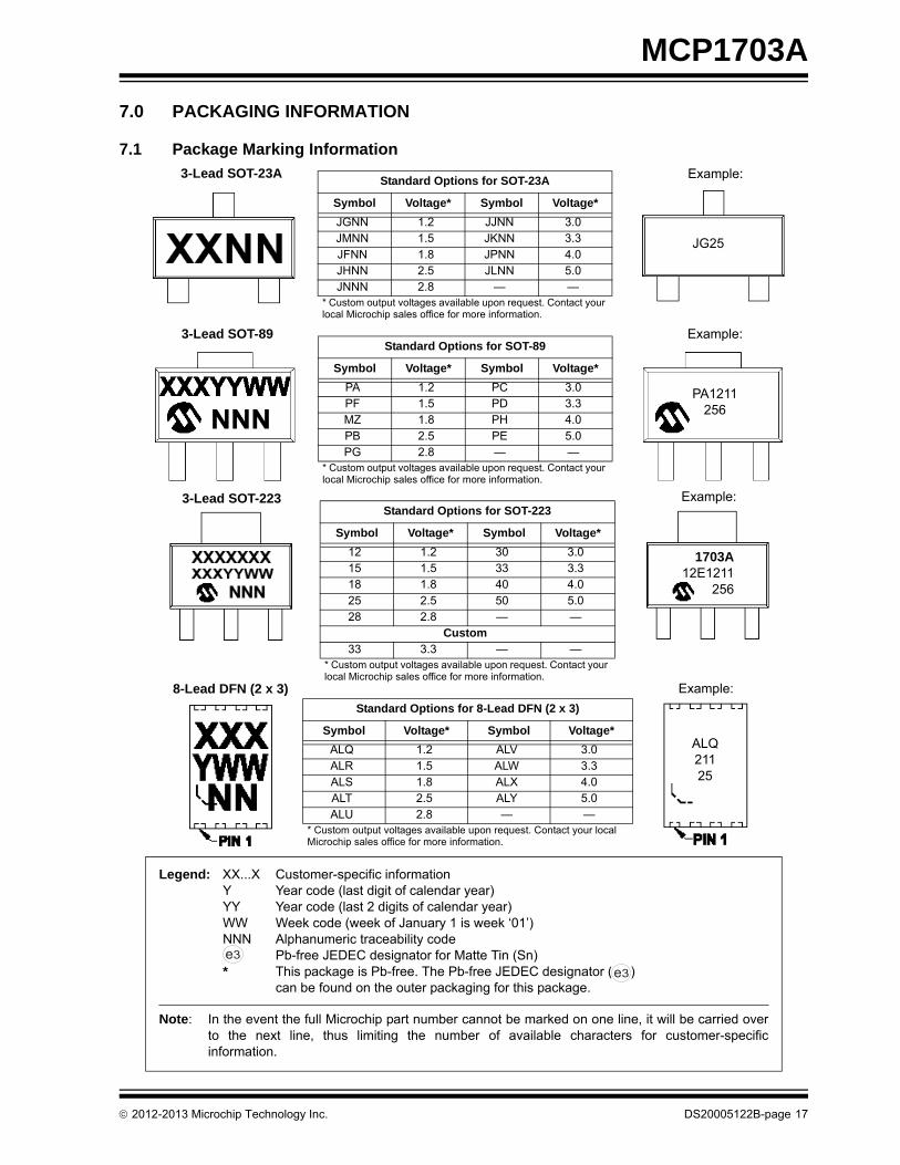
7.0 PACKAGING INFORMATION
7.1 Package Marking Information
3-Lead SOT-23A Example:
3-Lead SOT-89 Example:
JG25
Standard Options for SOT-23A
Symbol Voltage* Symbol Voltage*
JGNN 1.2 JJNN 3.0JMNN 1.5 JKNN 3.3JFNN 1.8 JPNN 4.0JHNN 2.5 JLNN 5.0JNNN 2.8 — —
* Custom output voltages available upon request. Contact your local Microchip sales office for more information.
Standard Options for SOT-89
Symbol Voltage* Symbol Voltage*
PA 1.2 PC 3.0PF 1.5 PD 3.3MZ 1.8 PH 4.0PB 2.5 PE 5.0PG 2.8 — —
* Custom output voltages available upon request. Contact your local Microchip sales office for more information.
PA1211256
3-Lead SOT-223 Example:Standard Options for SOT-223
Symbol Voltage* Symbol Voltage*
12 1.2 30 3.015 1.5 33 3.318 1.8 40 4.025 2.5 50 5.028 2.8 — —
Custom33 3.3 — —
* Custom output voltages available upon request. Contact your local Microchip sales office for more information.
1703A12E1211
256
ALQ21125
8-Lead DFN (2 x 3) Example:
Standard Options for 8-Lead DFN (2 x 3)
Symbol Voltage* Symbol Voltage*
ALQ 1.2 ALV 3.0ALR 1.5 ALW 3.3ALS 1.8 ALX 4.0ALT 2.5 ALY 5.0ALU 2.8 — —
* Custom output voltages available upon request. Contact your local Microchip sales office for more information.
Legend: XX...X Customer-specific informationY Year code (last digit of calendar year)YY Year code (last 2 digits of calendar year)WW Week code (week of January 1 is week ‘01’)NNN Alphanumeric traceability code Pb-free JEDEC designator for Matte Tin (Sn)* This package is Pb-free. The Pb-free JEDEC designator ( )
can be found on the outer packaging for this package.
Note: In the event the full Microchip part number cannot be marked on one line, it will be carried overto the next line, thus limiting the number of available characters for customer-specificinformation.
3e
3e
2012-2013 Microchip Technology Inc. DS20005122B-page 17
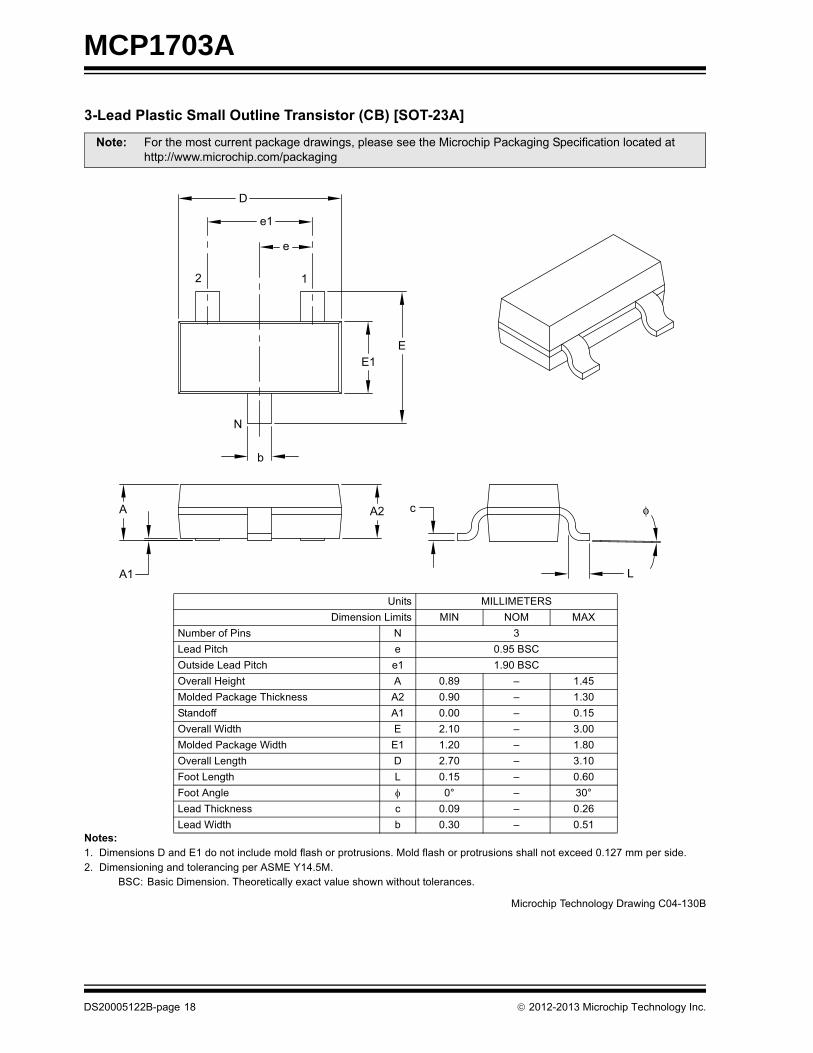
MCP1703A
�������� ������������������� � ���������������!
"��� #�� ��� � ��� �����!�"��!����#�����$! ����!�%�� �������#�$ ��� �����!�%�� �������#�$ ��� � �������#� &� !���������� �� �! ��� ��� � ���������!�#�� �������� �����"�'���(��
)�*+ )� ������ � ������� �� #������� &��#�,��$ � ��-��-�#��$#�#�� ���� �
"���# .���#� ��� #��$�� �#���/�� �!��-��� 0�� � � �#� ����������1��/������� ��%���#��������# !��#��##+22---�������������2��/�����
3��# ��44��"�"����� � ����4���# ��5 56� ��7
5$�8 ���%�1�� 5 �4 �!�1�#�� ���(�)�*6$# �! �4 �!�1�#�� � �����)�*6, �����9 ���# � ��:� ; ���(���! !�1��/�� �����/� �� ���� ; �����#��!�%% �� ���� ; ���(6, �����<�!#� " ���� ; �������! !�1��/�� �<�!#� "� ���� ; ��:�6, �����4 ��#� � ���� ; ����.��#�4 ��#� 4 ���( ; ��=�.��#����� � �> ; ��>4 �!�����/� � ���� ; ���=4 �!�<�!#� 8 ���� ; ��(�
D
e
e1
2 1
EE1
N
b
A
A1
A2 c
L
φ
�������� � �������� ���-��� *�����)
DS20005122B-page 18 2012-2013 Microchip Technology Inc.
MCP1703A
Note: For the most current package drawings, please see the Microchip Packaging Specification located at http://www.microchip.com/packaging
2012-2013 Microchip Technology Inc. DS20005122B-page 19
MCP1703A
�������� ������������������� � ���$�����%�������&'!
"��� #�� ��� � ��� �����!�"�!����#�����$! ����!�%�� �������#�$ ��� �����!�%�� �������#�$ ��� � �������#� &� !���������� �� �! ��� ��� � ���������!�#�� �������� �����"�'���(��
)�*+ )� ������ � ������� �� #������� &��#�,��$ � ��-��-�#��$#�#�� ���� �
"���# .���#� ��� #��$�� �#���/�� �!��-��� 0�� � � �#� ����������1��/������� ��%���#��������# !��#��##+22---�������������2��/�����
3��# ��44��"�"����� � ����4���# ��5 ��7
5$�8 ���%�4 �! 5 �1�#�� ��(��)�*6$# �! �4 �!�1�#�� � �����)�*6, �����9 ���# � ���� ��=�6, �����<�!#� 9 ���� ���(���! !�1��/�� �<�!#���#�)� " ���� ��=����! !�1��/�� �<�!#���#��� "� ���� ����6, �����4 ��#� � ���� ��=���8�4 ��#� �� ���� ��:�.��#�4 ��#� 4 ���� ����4 �!�����/� � ���( ����4 �!���<�!#� 8 ���� ��(=4 �! ���?���<�!#� 8� ���= ���:
D
D1
E
H
N
b1
e1
b
21
eb1
L
A
C
E1
�������� � �������� ���-��� *�����)
DS20005122B-page 20 2012-2013 Microchip Technology Inc.

MCP1703A
Note: For the most current package drawings, please see the Microchip Packaging Specification located at http://www.microchip.com/packaging
2012-2013 Microchip Technology Inc. DS20005122B-page 21
MCP1703A
�������� ������������������� � ����*����������!
"��� #�� ��� � ��� �����!�"��!����#�����$! ����!�%�� �������#�$ ��� �����!�%�� �������#�$ ��� � �������#� &� !���������� �� �! ��� ��� � ���������!�#�� �������� �����"�'���(��
)�*+ )� ������ � ������� �� #������� &��#�,��$ � ��-��-�#��$#�#�� ���� �
"���# .���#� ��� #��$�� �#���/�� �!��-��� 0�� � � �#� ����������1��/������� ��%���#��������# !��#��##+22---�������������2��/�����
3��# ��44��"�"����� � ����4���# ��5 56� ��7
5$�8 ���%�4 �! 5 �4 �!�1�#�� �����)�*6$# �! �4 �!�1�#�� � ��=��)�*6, �����9 ���# � ; ; ��:��#��!�%% �� ���� ; �������! !�1��/�� �9 ���# �� ��(� ��=� ����6, �����<�!#� " =��� ���� �������! !�1��/�� �<�!#� "� ���� ��(� ����6, �����4 ��#� � =��� =�(� =���4 �!�����/� � ���� ���� ���(4 �!�<�!#� 8 ��=� ���= ��:���8�4 �!�<�!#� 8� ���� ���� ����.��#�4 ��#� 4 ���( ; ;4 �!����� � �> ; ��>
D
b2
EE1
1 2 3
e
e1
A A2
A1b
c
L
φ
�������� � �������� ���-��� *�����)
DS20005122B-page 22 2012-2013 Microchip Technology Inc.
MCP1703A
�������� ������������������� � ����*����������!
"���# .���#� ��� #��$�� �#���/�� �!��-��� 0�� � � �#� ����������1��/������� ��%���#��������# !��#��##+22---�������������2��/�����
2012-2013 Microchip Technology Inc. DS20005122B-page 23
MCP1703A
&������� ���*���+���-"�������4�8��%��9�:�:;<'����>�*+"!
"��� #�� 1�����,� $�����! &�% �#$� �����,���0�8$#��$ #�8 �����# !�-�#����#� ���#�� !��� ���� 1��/�� �������, ��� ������� � &� !�#� �8�� ��#� �! ��� 1��/�� �� � �-� ���$��# !��� ��� � ���������!�#�� �������� �����"�'���(��
)�*+ )� ������ � ������� �� #������� &��#�,��$ � ��-��-�#��$#�#�� ���� ��".+ � % � �� ���� � ���0�$ $�����-�#��$#�#�� ���� 0�%�����%����#����$�� ������
"���# .���#� ��� #��$�� �#���/�� �!��-��� 0�� � � �#� ����������1��/������� ��%���#��������# !��#��##+22---�������������2��/�����
3��# ��44��"�"����� � ����4���# ��5 56� ��7
5$�8 ���%�1�� 5 :1�#�� ��(��)�*6, �����9 ���# � ��:� ���� �����#��!�%%� �� ���� ���� ���(*��#��#�����/� �� ������".6, �����4 ��#� � �����)�*6, �����<�!#� " �����)�*"&� !�1�!�4 ��#� �� ���� ; ��(("&� !�1�!�<�!#� "� ��(� ; ���(*��#��#�<�!#� 8 ���� ���( ����*��#��#�4 ��#� 4 ���� ���� ��(�*��#��##�"&� !�1�! @ ���� ; ;
D
N
E
NOTE 1
1 2
EXPOSED PAD
NOTE 12 1
D2
K
L
E2
N
eb
A3 A1
A
NOTE 2
BOTTOM VIEWTOP VIEW
�������� � �������� ���-��� *�����*
DS20005122B-page 24 2012-2013 Microchip Technology Inc.

MCP1703A
Note: For the most current package drawings, please see the Microchip Packaging Specification located at http://www.microchip.com/packaging
2012-2013 Microchip Technology Inc. DS20005122B-page 25
MCP1703A
NOTES:
DS20005122B-page 26 2012-2013 Microchip Technology Inc.

MCP1703A
APPENDIX A: REVISION HISTORY
Revision B (September 2013)
The following is the list of modifications:
1. Updated Figure 2-10, Figure 2-16, Figure 2-17,Figure 2-27, Figure 2-28, Figure 2-29 andFigure 2-30.
2. Minor grammatical and editorial corrections.
Revision A (March 2012)
• Original Release of this Document.
2012-2013 Microchip Technology Inc. DS20005122B-page 27

MCP1703A
NOTES:
2012-2013 Microchip Technology Inc. DS20005122B-page 28
2012-2013 Microchip Technology Inc. DS20005122B-page 28
MCP1703A
PRODUCT IDENTIFICATION SYSTEM
To order or obtain information, e.g., on pricing or delivery, refer to the factory or the listed sales office.
Device: MCP1703A: 250 mA, 16V Low Quiescent Current LDO
Tape and Reel: T = Tape and Reel
Output Voltage*: 12 = 1.2V “Standard”15 = 1.5V “Standard”18 = 1.8V “Standard”25 = 2.5V “Standard”28 = 2.8V “Standard”30 = 3.0V “Standard”33 = 3.3V “Standard”40 = 4.0V “Standard”50 = 5.0V “Standard”*Contact factory for other output voltage options.
Extra Feature Code: 0 = Fixed
Tolerance: 1 = 1.0% (Custom)
2 = 2.0% (Standard)
Temperature: E = -40°C to +125°C (Extended)
Package Type: CB = Plastic Small Outline Transistor (SOT-23A), 3-leadDB = Plastic Small Outline Transistor (SOT-223), 3-leadMB = Plastic Small Outline Transistor (SOT-89), 3-leadMC = Plastic Dual Flat, No Lead Package (DFN) -
2x3x0.9mm, 8-lead.
PART NO. XXX
Output FeatureCode
DeviceVoltage
X
Tolerance
X/
Temp.
XX
Package
X-
Tapeand Reel
Examples:
a) MCP1703AT-1202E/XX: Tape and Reel,1.2V Low Quiescent LDO,Extended Temperature
b) MCP1703AT-1502E/XX: Tape and Reel,1.5V Low Quiescent LDO,Extended Temperature
c) MCP1703AT-1802E/XX: Tape and Reel,1.8V Low Quiescent LDO,Extended Temperature
d) MCP1703AT-2502E/XX: Tape and Reel,2.5V Low Quiescent LDO,Extended Temperature
e) MCP1703AT-2802E/XX: Tape and Reel,2.8V Low Quiescent LDO,Extended Temperature
f) MCP1703AT-3002E/XX: Tape and Reel,3.0V Low Quiescent LDO,Extended Temperature
g) MCP1703AT-3302E/XX: Tape and Reel,3.3V Low Quiescent LDO,Extended Temperature
h) MCP1703AT-4002E/XX: Tape and Reel,4.0V Low Quiescent LDO,Extended Temperature
i) MCP1703AT-5002E/XX: Tape and Reel,5.0V Low Quiescent LDO,Extended Temperature
XX = CB for 3LD SOT-23A package= DB for 3LD SOT-223 package= MB for 3LD SOT-89 package= MC for 8LD DFN package.
Note the following details of the code protection feature on Microchip devices:
• Microchip products meet the specification contained in their particular Microchip Data Sheet.
• Microchip believes that its family of products is one of the most secure families of its kind on the market today, when used in the intended manner and under normal conditions.
• There are dishonest and possibly illegal methods used to breach the code protection feature. All of these methods, to our knowledge, require using the Microchip products in a manner outside the operating specifications contained in Microchip’s Data Sheets. Most likely, the person doing so is engaged in theft of intellectual property.
• Microchip is willing to work with the customer who is concerned about the integrity of their code.
• Neither Microchip nor any other semiconductor manufacturer can guarantee the security of their code. Code protection does not mean that we are guaranteeing the product as “unbreakable.”
Code protection is constantly evolving. We at Microchip are committed to continuously improving the code protection features of ourproducts. Attempts to break Microchip’s code protection feature may be a violation of the Digital Millennium Copyright Act. If such actsallow unauthorized access to your software or other copyrighted work, you may have a right to sue for relief under that Act.
Information contained in this publication regarding deviceapplications and the like is provided only for your convenienceand may be superseded by updates. It is your responsibility toensure that your application meets with your specifications.MICROCHIP MAKES NO REPRESENTATIONS ORWARRANTIES OF ANY KIND WHETHER EXPRESS ORIMPLIED, WRITTEN OR ORAL, STATUTORY OROTHERWISE, RELATED TO THE INFORMATION,INCLUDING BUT NOT LIMITED TO ITS CONDITION,QUALITY, PERFORMANCE, MERCHANTABILITY ORFITNESS FOR PURPOSE. Microchip disclaims all liabilityarising from this information and its use. Use of Microchipdevices in life support and/or safety applications is entirely atthe buyer’s risk, and the buyer agrees to defend, indemnify andhold harmless Microchip from any and all damages, claims,suits, or expenses resulting from such use. No licenses areconveyed, implicitly or otherwise, under any Microchipintellectual property rights.
2012-2013 Microchip Technology Inc.
QUALITY MANAGEMENT SYSTEM CERTIFIED BY DNV
== ISO/TS 16949 ==
Trademarks
The Microchip name and logo, the Microchip logo, dsPIC, FlashFlex, KEELOQ, KEELOQ logo, MPLAB, PIC, PICmicro, PICSTART, PIC32 logo, rfPIC, SST, SST Logo, SuperFlash and UNI/O are registered trademarks of Microchip Technology Incorporated in the U.S.A. and other countries.
FilterLab, Hampshire, HI-TECH C, Linear Active Thermistor, MTP, SEEVAL and The Embedded Control Solutions Company are registered trademarks of Microchip Technology Incorporated in the U.S.A.
Silicon Storage Technology is a registered trademark of Microchip Technology Inc. in other countries.
Analog-for-the-Digital Age, Application Maestro, BodyCom, chipKIT, chipKIT logo, CodeGuard, dsPICDEM, dsPICDEM.net, dsPICworks, dsSPEAK, ECAN, ECONOMONITOR, FanSense, HI-TIDE, In-Circuit Serial Programming, ICSP, Mindi, MiWi, MPASM, MPF, MPLAB Certified logo, MPLIB, MPLINK, mTouch, Omniscient Code Generation, PICC, PICC-18, PICDEM, PICDEM.net, PICkit, PICtail, REAL ICE, rfLAB, Select Mode, SQI, Serial Quad I/O, Total Endurance, TSHARC, UniWinDriver, WiperLock, ZENA and Z-Scale are trademarks of Microchip Technology Incorporated in the U.S.A. and other countries.
SQTP is a service mark of Microchip Technology Incorporated in the U.S.A.
GestIC and ULPP are registered trademarks of Microchip Technology Germany II GmbH & Co. KG, a subsidiary of Microchip Technology Inc., in other countries.
All other trademarks mentioned herein are property of their respective companies.
© 2012-2013, Microchip Technology Incorporated, Printed in the U.S.A., All Rights Reserved.
Printed on recycled paper.
ISBN: 978-1-62077-430-4
DS20005122B-page 29
Microchip received ISO/TS-16949:2009 certification for its worldwide headquarters, design and wafer fabrication facilities in Chandler and Tempe, Arizona; Gresham, Oregon and design centers in California and India. The Company’s quality system processes and procedures are for its PIC® MCUs and dsPIC® DSCs, KEELOQ® code hopping devices, Serial EEPROMs, microperipherals, nonvolatile memory and analog products. In addition, Microchip’s quality system for the design and manufacture of development systems is ISO 9001:2000 certified.

DS20005122B-page 30 2012-2013 Microchip Technology Inc.
AMERICASCorporate Office2355 West Chandler Blvd.Chandler, AZ 85224-6199Tel: 480-792-7200 Fax: 480-792-7277Technical Support: http://www.microchip.com/supportWeb Address: www.microchip.com
AtlantaDuluth, GA Tel: 678-957-9614 Fax: 678-957-1455
BostonWestborough, MA Tel: 774-760-0087 Fax: 774-760-0088
ChicagoItasca, IL Tel: 630-285-0071 Fax: 630-285-0075
ClevelandIndependence, OH Tel: 216-447-0464 Fax: 216-447-0643
DallasAddison, TX Tel: 972-818-7423 Fax: 972-818-2924
DetroitFarmington Hills, MI Tel: 248-538-2250Fax: 248-538-2260
IndianapolisNoblesville, IN Tel: 317-773-8323Fax: 317-773-5453
Los AngelesMission Viejo, CA Tel: 949-462-9523 Fax: 949-462-9608
Santa ClaraSanta Clara, CA Tel: 408-961-6444Fax: 408-961-6445
TorontoMississauga, Ontario, CanadaTel: 905-673-0699 Fax: 905-673-6509
ASIA/PACIFICAsia Pacific OfficeSuites 3707-14, 37th FloorTower 6, The GatewayHarbour City, KowloonHong KongTel: 852-2401-1200Fax: 852-2401-3431
Australia - SydneyTel: 61-2-9868-6733Fax: 61-2-9868-6755
China - BeijingTel: 86-10-8569-7000 Fax: 86-10-8528-2104
China - ChengduTel: 86-28-8665-5511Fax: 86-28-8665-7889
China - ChongqingTel: 86-23-8980-9588Fax: 86-23-8980-9500
China - HangzhouTel: 86-571-2819-3187 Fax: 86-571-2819-3189
China - Hong Kong SARTel: 852-2943-5100 Fax: 852-2401-3431
China - NanjingTel: 86-25-8473-2460Fax: 86-25-8473-2470
China - QingdaoTel: 86-532-8502-7355Fax: 86-532-8502-7205
China - ShanghaiTel: 86-21-5407-5533 Fax: 86-21-5407-5066
China - ShenyangTel: 86-24-2334-2829Fax: 86-24-2334-2393
China - ShenzhenTel: 86-755-8864-2200 Fax: 86-755-8203-1760
China - WuhanTel: 86-27-5980-5300Fax: 86-27-5980-5118
China - XianTel: 86-29-8833-7252Fax: 86-29-8833-7256
China - XiamenTel: 86-592-2388138 Fax: 86-592-2388130
China - ZhuhaiTel: 86-756-3210040 Fax: 86-756-3210049
ASIA/PACIFICIndia - BangaloreTel: 91-80-3090-4444 Fax: 91-80-3090-4123
India - New DelhiTel: 91-11-4160-8631Fax: 91-11-4160-8632
India - PuneTel: 91-20-3019-1500
Japan - OsakaTel: 81-6-6152-7160 Fax: 81-6-6152-9310
Japan - TokyoTel: 81-3-6880- 3770 Fax: 81-3-6880-3771
Korea - DaeguTel: 82-53-744-4301Fax: 82-53-744-4302
Korea - SeoulTel: 82-2-554-7200Fax: 82-2-558-5932 or 82-2-558-5934
Malaysia - Kuala LumpurTel: 60-3-6201-9857Fax: 60-3-6201-9859
Malaysia - PenangTel: 60-4-227-8870Fax: 60-4-227-4068
Philippines - ManilaTel: 63-2-634-9065Fax: 63-2-634-9069
SingaporeTel: 65-6334-8870Fax: 65-6334-8850
Taiwan - Hsin ChuTel: 886-3-5778-366Fax: 886-3-5770-955
Taiwan - KaohsiungTel: 886-7-213-7828Fax: 886-7-330-9305
Taiwan - TaipeiTel: 886-2-2508-8600 Fax: 886-2-2508-0102
Thailand - BangkokTel: 66-2-694-1351Fax: 66-2-694-1350
EUROPEAustria - WelsTel: 43-7242-2244-39Fax: 43-7242-2244-393Denmark - CopenhagenTel: 45-4450-2828 Fax: 45-4485-2829
France - ParisTel: 33-1-69-53-63-20 Fax: 33-1-69-30-90-79
Germany - MunichTel: 49-89-627-144-0 Fax: 49-89-627-144-44
Italy - Milan Tel: 39-0331-742611 Fax: 39-0331-466781
Netherlands - DrunenTel: 31-416-690399 Fax: 31-416-690340
Spain - MadridTel: 34-91-708-08-90Fax: 34-91-708-08-91
UK - WokinghamTel: 44-118-921-5869Fax: 44-118-921-5820
Worldwide Sales and Service
08/20/13


![Output LDO Regulators Ultra Low Quiescent Current LDO ...0 2 4 6 8 12 14 16 18 20 0 40 80 120 160 200 OUTPUT CURRENT : IOUT[mA]-40 C 25 C 125 C Total supply current vs. Load Figure](https://static.fdocuments.net/doc/165x107/61143a411c02b07ee452b42d/output-ldo-regulators-ultra-low-quiescent-current-ldo-0-2-4-6-8-12-14-16-18.jpg)