23 bits optical sensor based on nonvolatile organic memory ... · PDF fileSpatial profile of...
7
Title 23 bits optical sensor based on nonvolatile organic memory transistor Author(s) Ren, X; Chan, PKL Citation Applied Physics Letters, 2014, v. 104 n. 11, article no. 113302, p. 113302:1-113302:5 Issued Date 2014 URL http://hdl.handle.net/10722/199131 Rights Applied Physics Letters. Copyright © American Institute of Physics.
Transcript of 23 bits optical sensor based on nonvolatile organic memory ... · PDF fileSpatial profile of...
Title 23 bits optical sensor based on nonvolatile organic memorytransistor
Author(s) Ren, X; Chan, PKL
Citation Applied Physics Letters, 2014, v. 104 n. 11, article no. 113302, p.113302:1-113302:5
Issued Date 2014
URL http://hdl.handle.net/10722/199131
Rights Applied Physics Letters. Copyright © American Institute ofPhysics.
23 bits optical sensor based on nonvolatile organic memory transistorXiaochen Ren and Paddy K. L. Chan Citation: Applied Physics Letters 104, 113302 (2014); doi: 10.1063/1.4869308 View online: http://dx.doi.org/10.1063/1.4869308 View Table of Contents: http://scitation.aip.org/content/aip/journal/apl/104/11?ver=pdfcov Published by the AIP Publishing Articles you may be interested in Ambipolar organic thin-film transistor-based nano-floating-gate nonvolatile memory Appl. Phys. Lett. 104, 013302 (2014); 10.1063/1.4860990 Spatial profile of charge storage in organic field-effect transistor nonvolatile memory using polymer electret Appl. Phys. Lett. 103, 143302 (2013); 10.1063/1.4824213 Nonvolatile memory thin film transistors using CdSe/ZnS quantum dot-poly(methyl methacrylate) composite layerformed by a two-step spin coating technique J. Appl. Phys. 112, 034518 (2012); 10.1063/1.4745041 Nonvolatile organic transistor-memory devices using various thicknesses of silver nanoparticle layers Appl. Phys. Lett. 97, 023511 (2010); 10.1063/1.3462949 Nonvolatile organic field-effect transistor memory element with a polymeric gate electret Appl. Phys. Lett. 85, 5409 (2004); 10.1063/1.1828236
This article is copyrighted as indicated in the article. Reuse of AIP content is subject to the terms at: http://scitation.aip.org/termsconditions. Downloaded to IP: 147.8.31.43
On: Tue, 25 Nov 2014 06:21:11
23 bits optical sensor based on nonvolatile organic memory transistor
Xiaochen Ren and Paddy K. L. Chana)
Department of Mechanical Engineering, The University of Hong Kong, Hong Kong
(Received 13 November 2013; accepted 11 March 2014; published online 20 March 2014)
Polymer electret transistor memory device has stable charge storage and memory properties. Here,
we combine a large band gap organic semiconductor dinaphtho[2,3-b:20,30-f]thieno[3,2-
b]thiophene with the polystyrene electret to form an optical sensor with memory effect. The blue
light combined with programming bias leads to a positive threshold voltage shift for more than
100 V while the drain-source current shows a variation of seven orders of magnitude. The dynamic
range of current device is up to 23 bits and the photo responsivity is 420 A W�1. The optically
programmed transistor can be directly used for high-resolution optical sensor and multi-level data
storage applications. VC 2014 AIP Publishing LLC. [http://dx.doi.org/10.1063/1.4869308]
Organic field effect transistors (OFETs) have demon-
strated their potential applications in various functional devi-
ces including memories1 and integrated sensors.2 In memory
transistors, the carrier density in the channel region is pre-
cisely controlled by the local electrical field induced by trap
charges that are generated by electrical bias or external stimu-
lations such as pressure and light. Different structures have
been realized for organic memory transistor, such as inserting
the floating gate layer,1 using polymer electrets as charge
trapping media,3 and placing metal nanoparticles into dielec-
tric4 or semiconductor5 as the charge trapping centers.
Among these structures, polymer electret has demonstrated
high writing/erasing speed with long charge retention prop-
erty.6,7 Baeg et al. has reported transistor memory devices
based on different polymer electrets and most of the devices
can be programmed within few millisecond (ms) and the pro-
gramming states can be maintained over 1000 s without
significant degradation and it is expected that the retention
time of memory transistor based on polystyrene (PS) electret
could be close to 108 s.3 Hsu et al. reported the charge trap-
ping property of pentacene transistor with polystyrene
para-substituted with p-conjugated oligofluorenes as polymer
electrets.8 They showed the p-conjugated oligofluorenes with
smaller band gap can offer larger threshold voltage (Vth) shift
because of the lower injection barrier for electrons.8 In
polymer electrets memory devices, pentacene is commonly
used as the active layer p-type semiconductor materials.9,10
Compare with pentacene, transistors made with dinaph-
tho-[2,3-b:20,30-f]-thieno[3,2-b]thiophene (DNTT) cannot
only provide high field-effect mobility for high frequency
operation,11 but more importantly, DNTT device can operate
under high temperature environment up to 150 �C and ambi-
ent air environment without encapsulation.12,13
Other than memory devices, OFETs can also be used for
sensing physical parameters including pressure,2 tempera-
ture,14 and light.15 Optical sensors for different photon wave-
lengths can be tuned by varying the molecular structure thus
the band gap of organic semiconductors.16 Small molecular
weight organic semiconductor phototransistors have similar
photo responsivity (R—the ratio between the photo-
generated current and the incident light intensity) and
dynamic range (DR—ratio between maximum and minimum
output signal of a sensor) to their inorganic counterparts.
Owing to the high mobility of graphene, the highest reported
R of organic transistor was graphene-based devices with a
value over 105 A W�1.17 However, the DR of the graphene
transistor is very low because of the high off current in the
device. On the other hand, the small molecular weight
organic semiconductor transistors offer large light/dark
current ratio (103–105) (i.e., high dynamic range), but
suffer from low responsivity due to their low mobility
(0.02–0.5 cm2 V�1 s�1).18 Recently, several groups have
demonstrated the integration of the photosensing and mem-
ory properties of organic transistor into a single device by
maintaining the photo excited charges in the device. This
can be done by using ultrathin dielectric,19 photochromic
materials,20,21 or charge trapping small molecule layer.22
Zhang et al. have demonstrated the light-charge organic tran-
sistor memory (LCOM) devices with the low-lying lowest
unoccupied molecular orbital (LUMO) energy level small
molecule organic semiconductor as the charge storage mate-
rial.22 In LCOM, photo-generated electrons are stored in the
small molecule charge trapping centers due to its low con-
ductivity and low-lying LUMO energy level. The charge
retention time and on/off ratio of the devices can be as high
as 20 000 s and 103, respectively.
In this work, we combine the optical sensing and mem-
ory properties of the OFETs by using electret material and
large band gap organic semiconductor to form a high per-
formance optical programming memory transistor. We used
the air stable organic semiconductor with large band gap,
DNTT (3 eV), as the active layer material and PS/SiO2 as the
hybrid dielectric. The Vth of the transistors can be altered in
both positive and negative directions by applying external
gate bias with light irradiation. The shift of Vth shows no
degradation for longer than 104 s and it is believed that the
charge retention time can be longer than 107 s. The current
optical memory transistor with controllable Vth shift under
various light intensities has responsivity of 420 A W�1 and
high dynamic range of 23 bits which can be use directly as
an optical sensors and multi-level storage memories.
The cross-section SEM image together with schematic
diagram of the device is shown in Fig. 1(a). The device fab-
rication process is described as follow. Heavily doped Sia)Email: [email protected]
0003-6951/2014/104(11)/113302/5/$30.00 VC 2014 AIP Publishing LLC104, 113302-1
APPLIED PHYSICS LETTERS 104, 113302 (2014)
This article is copyrighted as indicated in the article. Reuse of AIP content is subject to the terms at: http://scitation.aip.org/termsconditions. Downloaded to IP: 147.8.31.43
On: Tue, 25 Nov 2014 06:21:11
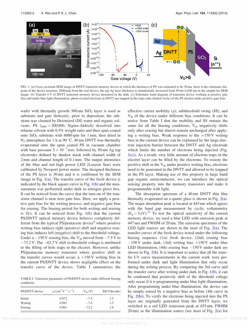
wafer with thermally growth 300 nm SiO2 layer is used as
substrate and gate dielectric, prior to deposition, the sub-
strate was cleaned by Deionized (DI) water and organic sol-
vents. PS (MW¼ 200 000, Sigma-Aldrich) dissolved into
toluene solvent with 0.5% weight ratio and then spun coated
onto SiO2 substrate with 6000 rpm for 1 min, then dried in
N2 atmosphere for 1 h at 90 �C. 40 nm DNTT was thermally
evaporated onto the spun coated PS in vacuum chamber
with base pressure 5� 10�7 torr, followed by 50 nm Ag top
electrodes defined by shadow mask with channel width of
2 mm and channel length of 0.1 mm. The output intensities
of the blue and red high power LED (Luxeon Star) were
calibrated by Newport power meter. The designed thickness
of the PS layer is 30 nm and it is confirmed by the SEM
image in Fig. 1(a). The transfer curve of the fresh device is
indicated by the black square curve in Fig. 1(b) and the mea-
surement was performed under dark in nitrogen glove box.
It can be noticed from the curve that the turn-on of the tran-
sistor channel is near zero gate bias. Here, we apply a posi-
tive gate bias for the writing process, and negative gate bias
for erasing. The biasing period for both writing and erasing
is 10 s. It can be noticed from Fig. 1(b) that the current
PS/DNTT optical memory device behaves completely dif-
ferent from the typical PS/pentacene device6 where positive
writing bias induces right (positive) shift and negative eras-
ing bias induces left (negative) shift to the threshold voltage.
Under a �150 V erasing bias, the Vth moved from �7.5 V to
�73.2 V. The �63.7 V shift in threshold voltage is attributed
to the filling of hole traps in the electret. However, unlike
PS/pentacene memory transistor where positive shift in
the transfer curves would occur, a þ150 V writing bias in
the current PS/DNTT device shows negligible effect on the
transfer curve of the device. Table I summarizes the
effective carrier mobility (l), subthreshold swing (SS), and
Vth of the device under different bias conditions. It can be
notice from Table I that the mobility and SS remain the
same for all the biasing conditions, Vth negatively shifts
only after erasing but almost remain unchanged after apply-
ing a writing bias. Weak response to the þ150 V writing
bias in the current device can be explained by the large elec-
tron injection barrier between the DNTT and Ag electrode
which limits the number of electrons being injected (Fig.
1(c)). As a result, very little amount of electron traps in the
electret layer can be filled by the electrons. To restore the
positive shift in the Vth under positive writing bias, electrons
need to be generated in the DNTT and allowed to be trapped
in the PS layer. Making use of this property in large band
gap organic semiconductor, we can introduce the optical
sensing property into the memory transistors and make it
programmable with light.
The absorption spectrum of a 40 nm DNTT thin film
thermally evaporated on a quartz glass is shown in Fig. 2(a).
The major absorption peak is located at 443 nm which agrees
with the band gap measurement by cyclic voltammetry
(Eg¼ 3 eV).23 To test the optical sensitivity of the current
memory device, we used a blue LED with emission peak at
447 nm and FWHM of 20 nm. The emission spectrums of the
LED light sources are shown in the inset of Fig. 2(a). The
transfer curves of the fresh device tested under the following
biasing sequence (1st) fresh device, (2nd) erasing bias
�150 V under dark, (3rd) writing bias þ150 V under blue
LED illumination, (4th) erasing bias �150 V under dark are
shown in Fig. 2(b). It is important to notice that all the trans-
fer I-V curve measurements in the current work were per-
formed under dark and light illumination that only occur
during the writing process. By comparing the 3rd curve and
the transfer curve after writing under dark in Fig. 1(b), it can
be confirmed that positively shift of the threshold voltage
only occur if it is programming under blue light illumination.
After programming under blue illumination, the device can
be simply erased by a negative bias as before (4th curve in
Fig. 2(b)). To verify the electrons being injected into the PS
layer are originally generated from the DNTT layer, we
switched to a red LED (emission peak at 655 nm, FWHM
20 nm) as the illumination source (see inset of Fig. 2(a) for
FIG. 1. (a) Cross sectional SEM image of DNTT transistor memory device in which the thickness of PS was estimated to be 30 nm. Inset is the schematic dia-
gram of the device structure. Different from the real device, the top Ag layer thickness is intentionally increased from 50 nm to100 nm in the sample for SEM
image. (b) Transfer I-V of DNTT transistor memory device measured in the dark. (c) Schematic band diagram of transistor device working at positive gate
bias and under blue light illumination, photo excited electrons in DNTT are trapped in the traps state (dotted circle) of the PS electret under positive gate bias.
TABLE I. Transistor parameters of PS/DNTT device under different biasing
conditions.
PS/DNTT device l (cm2 V�1 s�1) Vth (V) SS(V/decade)
Initial 0.972 �7.5 1.5
Writing 0.981 �7.4 1.5
Erasing 0.961 �73.2 1.6
113302-2 X. Ren and P. K. L. Chan Appl. Phys. Lett. 104, 113302 (2014)
This article is copyrighted as indicated in the article. Reuse of AIP content is subject to the terms at: http://scitation.aip.org/termsconditions. Downloaded to IP: 147.8.31.43
On: Tue, 25 Nov 2014 06:21:11
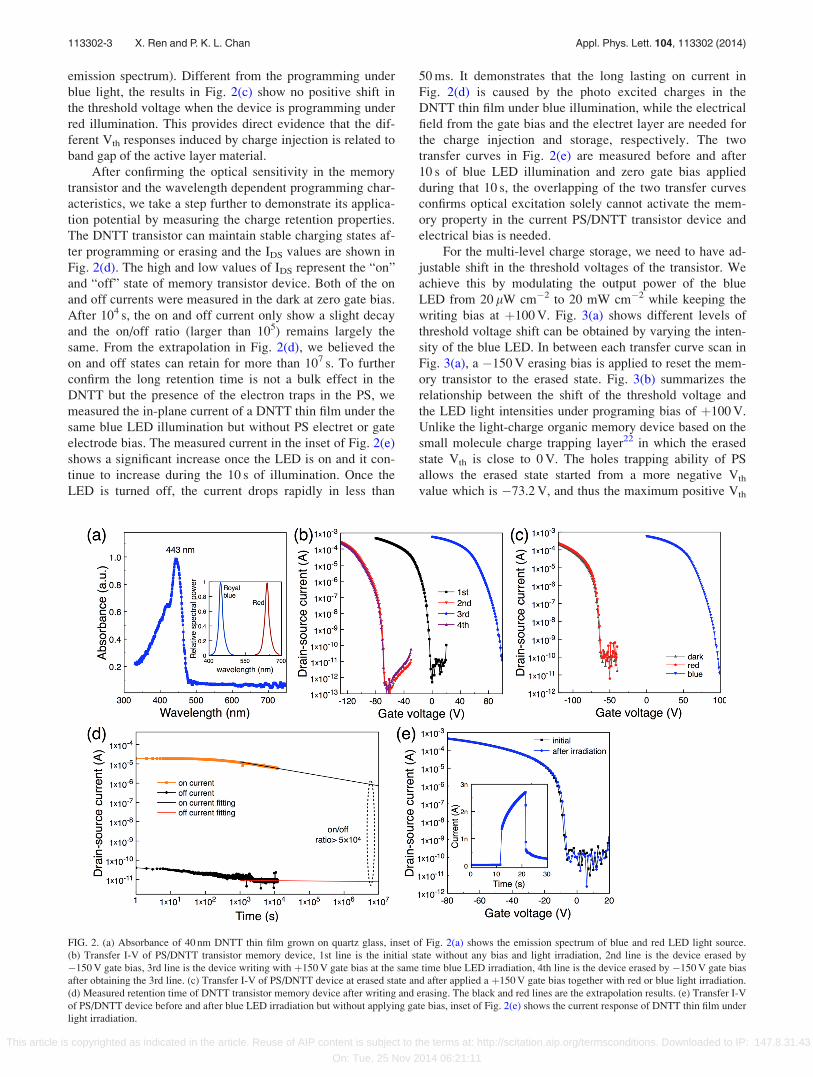
emission spectrum). Different from the programming under
blue light, the results in Fig. 2(c) show no positive shift in
the threshold voltage when the device is programming under
red illumination. This provides direct evidence that the dif-
ferent Vth responses induced by charge injection is related to
band gap of the active layer material.
After confirming the optical sensitivity in the memory
transistor and the wavelength dependent programming char-
acteristics, we take a step further to demonstrate its applica-
tion potential by measuring the charge retention properties.
The DNTT transistor can maintain stable charging states af-
ter programming or erasing and the IDS values are shown in
Fig. 2(d). The high and low values of IDS represent the “on”
and “off” state of memory transistor device. Both of the on
and off currents were measured in the dark at zero gate bias.
After 104 s, the on and off current only show a slight decay
and the on/off ratio (larger than 105) remains largely the
same. From the extrapolation in Fig. 2(d), we believed the
on and off states can retain for more than 107 s. To further
confirm the long retention time is not a bulk effect in the
DNTT but the presence of the electron traps in the PS, we
measured the in-plane current of a DNTT thin film under the
same blue LED illumination but without PS electret or gate
electrode bias. The measured current in the inset of Fig. 2(e)
shows a significant increase once the LED is on and it con-
tinue to increase during the 10 s of illumination. Once the
LED is turned off, the current drops rapidly in less than
50 ms. It demonstrates that the long lasting on current in
Fig. 2(d) is caused by the photo excited charges in the
DNTT thin film under blue illumination, while the electrical
field from the gate bias and the electret layer are needed for
the charge injection and storage, respectively. The two
transfer curves in Fig. 2(e) are measured before and after
10 s of blue LED illumination and zero gate bias applied
during that 10 s, the overlapping of the two transfer curves
confirms optical excitation solely cannot activate the mem-
ory property in the current PS/DNTT transistor device and
electrical bias is needed.
For the multi-level charge storage, we need to have ad-
justable shift in the threshold voltages of the transistor. We
achieve this by modulating the output power of the blue
LED from 20 lW cm�2 to 20 mW cm�2 while keeping the
writing bias at þ100 V. Fig. 3(a) shows different levels of
threshold voltage shift can be obtained by varying the inten-
sity of the blue LED. In between each transfer curve scan in
Fig. 3(a), a �150 V erasing bias is applied to reset the mem-
ory transistor to the erased state. Fig. 3(b) summarizes the
relationship between the shift of the threshold voltage and
the LED light intensities under programing bias of þ100 V.
Unlike the light-charge organic memory device based on the
small molecule charge trapping layer22 in which the erased
state Vth is close to 0 V. The holes trapping ability of PS
allows the erased state started from a more negative Vth
value which is �73.2 V, and thus the maximum positive Vth
FIG. 2. (a) Absorbance of 40 nm DNTT thin film grown on quartz glass, inset of Fig. 2(a) shows the emission spectrum of blue and red LED light source.
(b) Transfer I-V of PS/DNTT transistor memory device, 1st line is the initial state without any bias and light irradiation, 2nd line is the device erased by
�150 V gate bias, 3rd line is the device writing with þ150 V gate bias at the same time blue LED irradiation, 4th line is the device erased by �150 V gate bias
after obtaining the 3rd line. (c) Transfer I-V of PS/DNTT device at erased state and after applied a þ150 V gate bias together with red or blue light irradiation.
(d) Measured retention time of DNTT transistor memory device after writing and erasing. The black and red lines are the extrapolation results. (e) Transfer I-V
of PS/DNTT device before and after blue LED irradiation but without applying gate bias, inset of Fig. 2(e) shows the current response of DNTT thin film under
light irradiation.
113302-3 X. Ren and P. K. L. Chan Appl. Phys. Lett. 104, 113302 (2014)
This article is copyrighted as indicated in the article. Reuse of AIP content is subject to the terms at: http://scitation.aip.org/termsconditions. Downloaded to IP: 147.8.31.43
On: Tue, 25 Nov 2014 06:21:11
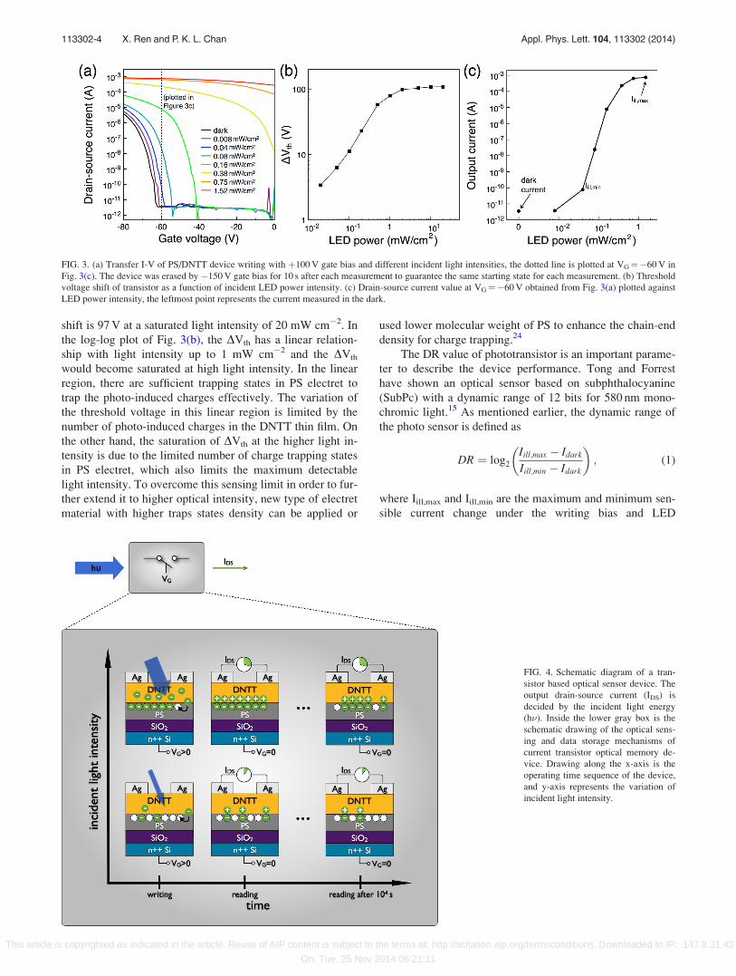
shift is 97 V at a saturated light intensity of 20 mW cm�2. In
the log-log plot of Fig. 3(b), the DVth has a linear relation-
ship with light intensity up to 1 mW cm�2 and the DVth
would become saturated at high light intensity. In the linear
region, there are sufficient trapping states in PS electret to
trap the photo-induced charges effectively. The variation of
the threshold voltage in this linear region is limited by the
number of photo-induced charges in the DNTT thin film. On
the other hand, the saturation of DVth at the higher light in-
tensity is due to the limited number of charge trapping states
in PS electret, which also limits the maximum detectable
light intensity. To overcome this sensing limit in order to fur-
ther extend it to higher optical intensity, new type of electret
material with higher traps states density can be applied or
used lower molecular weight of PS to enhance the chain-end
density for charge trapping.24
The DR value of phototransistor is an important parame-
ter to describe the device performance. Tong and Forrest
have shown an optical sensor based on subphthalocyanine
(SubPc) with a dynamic range of 12 bits for 580 nm mono-
chromic light.15 As mentioned earlier, the dynamic range of
the photo sensor is defined as
DR ¼ log2
Iill;max � Idark
Iill;min � Idark
� �; (1)
where Iill,max and Iill,min are the maximum and minimum sen-
sible current change under the writing bias and LED
FIG. 3. (a) Transfer I-V of PS/DNTT device writing with þ100 V gate bias and different incident light intensities, the dotted line is plotted at VG¼�60 V in
Fig. 3(c). The device was erased by �150 V gate bias for 10 s after each measurement to guarantee the same starting state for each measurement. (b) Threshold
voltage shift of transistor as a function of incident LED power intensity. (c) Drain-source current value at VG¼�60 V obtained from Fig. 3(a) plotted against
LED power intensity, the leftmost point represents the current measured in the dark.
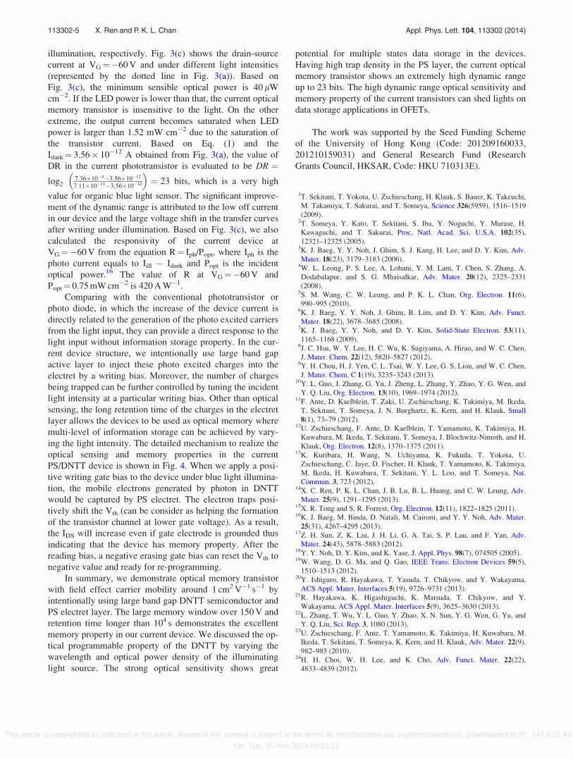
FIG. 4. Schematic diagram of a tran-
sistor based optical sensor device. The
output drain-source current (IDS) is
decided by the incident light energy
(h�). Inside the lower gray box is the
schematic drawing of the optical sens-
ing and data storage mechanisms of
current transistor optical memory de-
vice. Drawing along the x-axis is the
operating time sequence of the device,
and y-axis represents the variation of
incident light intensity.
113302-4 X. Ren and P. K. L. Chan Appl. Phys. Lett. 104, 113302 (2014)
This article is copyrighted as indicated in the article. Reuse of AIP content is subject to the terms at: http://scitation.aip.org/termsconditions. Downloaded to IP: 147.8.31.43
On: Tue, 25 Nov 2014 06:21:11
illumination, respectively. Fig. 3(c) shows the drain-source
current at VG¼�60 V and under different light intensities
(represented by the dotted line in Fig. 3(a)). Based on
Fig. 3(c), the minimum sensible optical power is 40 lW
cm�2. If the LED power is lower than that, the current optical
memory transistor is insensitive to the light. On the other
extreme, the output current becomes saturated when LED
power is larger than 1.52 mW cm�2 due to the saturation of
the transistor current. Based on Eq. (1) and the
Idark¼ 3.56� 10�12 A obtained from Fig. 3(a), the value of
DR in the current phototransistor is evaluated to be DR ¼log2
7:36�10�4�3:56�10�12
7:11�10�11�3:56�10�12
� �¼ 23 bits, which is a very high
value for organic blue light sensor. The significant improve-
ment of the dynamic range is attributed to the low off current
in our device and the large voltage shift in the transfer curves
after writing under illumination. Based on Fig. 3(c), we also
calculated the responsivity of the current device at
VG¼�60 V from the equation R¼ Iph/Popt, where Iph is the
photo current equals to Iill � Idark and Popt is the incident
optical power.16 The value of R at VG¼�60 V and
Popt¼ 0.75 mW cm�2 is 420 A W�1.
Comparing with the conventional phototransistor or
photo diode, in which the increase of the device current is
directly related to the generation of the photo excited carriers
from the light input, they can provide a direct response to the
light input without information storage property. In the cur-
rent device structure, we intentionally use large band gap
active layer to inject these photo excited charges into the
electret by a writing bias. Moreover, the number of charges
being trapped can be further controlled by tuning the incident
light intensity at a particular writing bias. Other than optical
sensing, the long retention time of the charges in the electret
layer allows the devices to be used as optical memory where
multi-level of information storage can be achieved by vary-
ing the light intensity. The detailed mechanism to realize the
optical sensing and memory properties in the current
PS/DNTT device is shown in Fig. 4. When we apply a posi-
tive writing gate bias to the device under blue light illumina-
tion, the mobile electrons generated by photon in DNTT
would be captured by PS electret. The electron traps posi-
tively shift the Vth (can be consider as helping the formation
of the transistor channel at lower gate voltage). As a result,
the IDS will increase even if gate electrode is grounded thus
indicating that the device has memory property. After the
reading bias, a negative erasing gate bias can reset the Vth to
negative value and ready for re-programming.
In summary, we demonstrate optical memory transistor
with field effect carrier mobility around 1 cm2 V�1 s�1 by
intentionally using large band gap DNTT semiconductor and
PS electret layer. The large memory window over 150 V and
retention time longer than 104 s demonstrates the excellent
memory property in our current device. We discussed the op-
tical programmable property of the DNTT by varying the
wavelength and optical power density of the illuminating
light source. The strong optical sensitivity shows great
potential for multiple states data storage in the devices.
Having high trap density in the PS layer, the current optical
memory transistor shows an extremely high dynamic range
up to 23 bits. The high dynamic range optical sensitivity and
memory property of the current transistors can shed lights on
data storage applications in OFETs.
The work was supported by the Seed Funding Scheme
of the University of Hong Kong (Code: 201209160033,
201210159031) and General Research Fund (Research
Grants Council, HKSAR, Code: HKU 710313E).
1T. Sekitani, T. Yokota, U. Zschieschang, H. Klauk, S. Bauer, K. Takeuchi,
M. Takamiya, T. Sakurai, and T. Someya, Science 326(5959), 1516–1519
(2009).2T. Someya, Y. Kato, T. Sekitani, S. Iba, Y. Noguchi, Y. Murase, H.
Kawaguchi, and T. Sakurai, Proc. Natl. Acad. Sci. U.S.A. 102(35),
12321–12325 (2005).3K. J. Baeg, Y. Y. Noh, J. Ghim, S. J. Kang, H. Lee, and D. Y. Kim, Adv.
Mater. 18(23), 3179–3183 (2006).4W. L. Leong, P. S. Lee, A. Lohani, Y. M. Lam, T. Chen, S. Zhang, A.
Dodabalapur, and S. G. Mhaisalkar, Adv. Mater. 20(12), 2325–2331
(2008).5S. M. Wang, C. W. Leung, and P. K. L. Chan, Org. Electron. 11(6),
990–995 (2010).6K. J. Baeg, Y. Y. Noh, J. Ghim, B. Lim, and D. Y. Kim, Adv. Funct.
Mater. 18(22), 3678–3685 (2008).7K. J. Baeg, Y. Y. Noh, and D. Y. Kim, Solid-State Electron. 53(11),
1165–1168 (2009).8J. C. Hsu, W. Y. Lee, H. C. Wu, K. Sugiyama, A. Hirao, and W. C. Chen,
J. Mater. Chem. 22(12), 5820–5827 (2012).9Y. H. Chou, H. J. Yen, C. L. Tsai, W. Y. Lee, G. S. Liou, and W. C. Chen,
J. Mater. Chem. C 1(19), 3235–3243 (2013).10Y. L. Guo, J. Zhang, G. Yu, J. Zheng, L. Zhang, Y. Zhao, Y. G. Wen, and
Y. Q. Liu, Org. Electron. 13(10), 1969–1974 (2012).11F. Ante, D. Kaelblein, T. Zaki, U. Zschieschang, K. Takimiya, M. Ikeda,
T. Sekitani, T. Someya, J. N. Burghartz, K. Kern, and H. Klauk, Small
8(1), 73–79 (2012).12U. Zschieschang, F. Ante, D. Kaelblein, T. Yamamoto, K. Takimiya, H.
Kuwabara, M. Ikeda, T. Sekitani, T. Someya, J. Blochwitz-Nimoth, and H.
Klauk, Org. Electron. 12(8), 1370–1375 (2011).13K. Kuribara, H. Wang, N. Uchiyama, K. Fukuda, T. Yokota, U.
Zschieschang, C. Jaye, D. Fischer, H. Klauk, T. Yamamoto, K. Takimiya,
M. Ikeda, H. Kuwabara, T. Sekitani, Y. L. Loo, and T. Someya, Nat.
Commun. 3, 723 (2012).14X. C. Ren, P. K. L. Chan, J. B. Lu, B. L. Huang, and C. W. Leung, Adv.
Mater. 25(9), 1291–1295 (2013).15X. R. Tong and S. R. Forrest, Org. Electron. 12(11), 1822–1825 (2011).16K. J. Baeg, M. Binda, D. Natali, M. Caironi, and Y. Y. Noh, Adv. Mater.
25(31), 4267–4295 (2013).17Z. H. Sun, Z. K. Liu, J. H. Li, G. A. Tai, S. P. Lau, and F. Yan, Adv.
Mater. 24(43), 5878–5883 (2012).18Y. Y. Noh, D. Y. Kim, and K. Yase, J. Appl. Phys. 98(7), 074505 (2005).19W. Wang, D. G. Ma, and Q. Gao, IEEE Trans. Electron Devices 59(5),
1510–1513 (2012).20Y. Ishiguro, R. Hayakawa, T. Yasuda, T. Chikyow, and Y. Wakayama,
ACS Appl. Mater. Interfaces 5(19), 9726–9731 (2013).21R. Hayakawa, K. Higashiguchi, K. Matsuda, T. Chikyow, and Y.
Wakayama, ACS Appl. Mater. Interfaces 5(9), 3625–3630 (2013).22L. Zhang, T. Wu, Y. L. Guo, Y. Zhao, X. N. Sun, Y. G. Wen, G. Yu, and
Y. Q. Liu, Sci. Rep. 3, 1080 (2013).23U. Zschieschang, F. Ante, T. Yamamoto, K. Takimiya, H. Kuwabara, M.
Ikeda, T. Sekitani, T. Someya, K. Kern, and H. Klauk, Adv. Mater. 22(9),
982–985 (2010).24H. H. Choi, W. H. Lee, and K. Cho, Adv. Funct. Mater. 22(22),
4833–4839 (2012).
113302-5 X. Ren and P. K. L. Chan Appl. Phys. Lett. 104, 113302 (2014)
This article is copyrighted as indicated in the article. Reuse of AIP content is subject to the terms at: http://scitation.aip.org/termsconditions. Downloaded to IP: 147.8.31.43
On: Tue, 25 Nov 2014 06:21:11