2.25 V low-voltage local digital temperature...
36
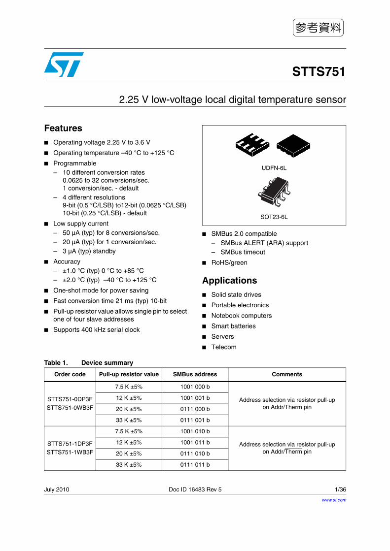
July 2010 Doc ID 16483 Rev 5 1/36 1 STTS751 2.25 V low-voltage local digital temperature sensor Features ■ Operating voltage 2.25 V to 3.6 V ■ Operating temperature –40 °C to +125 °C ■ Programmable – 10 different conversion rates 0.0625 to 32 conversions/sec. 1 conversion/sec. - default – 4 different resolutions 9-bit (0.5 °C/LSB) to12-bit (0.0625 °C/LSB) 10-bit (0.25 °C/LSB) - default ■ Low supply current – 50 μA (typ) for 8 conversions/sec. – 20 μA (typ) for 1 conversion/sec. – 3 μA (typ) standby ■ Accuracy – ±1.0 °C (typ) 0 °C to +85 °C – ±2.0 °C (typ) –40 °C to +125 °C ■ One-shot mode for power saving ■ Fast conversion time 21 ms (typ) 10-bit ■ Pull-up resistor value allows single pin to select one of four slave addresses ■ Supports 400 kHz serial clock ■ SMBus 2.0 compatible – SMBus ALERT (ARA) support – SMBus timeout ■ RoHS/green Applications ■ Solid state drives ■ Portable electronics ■ Notebook computers ■ Smart batteries ■ Servers ■ Telecom UDFN-6L SOT23-6L Table 1. Device summary Order code Pull-up resistor value SMBus address Comments STTS751-0DP3F STTS751-0WB3F 7.5 K ±5% 1001 000 b Address selection via resistor pull-up on Addr/Therm pin 12 K ±5% 1001 001 b 20 K ±5% 0111 000 b 33 K ±5% 0111 001 b STTS751-1DP3F STTS751-1WB3F 7.5 K ±5% 1001 010 b Address selection via resistor pull-up on Addr/Therm pin 12 K ±5% 1001 011 b 20 K ±5% 0111 010 b 33 K ±5% 0111 011 b www.st.com 参考資料
Transcript of 2.25 V low-voltage local digital temperature...
July 2010 Doc ID 16483 Rev 5 1/36
1
STTS751
2.25 V low-voltage local digital temperature sensor
Features■ Operating voltage 2.25 V to 3.6 V
■ Operating temperature –40 °C to +125 °C
■ Programmable– 10 different conversion rates
0.0625 to 32 conversions/sec. 1 conversion/sec. - default
– 4 different resolutions 9-bit (0.5 °C/LSB) to12-bit (0.0625 °C/LSB) 10-bit (0.25 °C/LSB) - default
■ Low supply current– 50 µA (typ) for 8 conversions/sec.– 20 µA (typ) for 1 conversion/sec.– 3 µA (typ) standby
■ Accuracy– ±1.0 °C (typ) 0 °C to +85 °C – ±2.0 °C (typ) –40 °C to +125 °C
■ One-shot mode for power saving
■ Fast conversion time 21 ms (typ) 10-bit
■ Pull-up resistor value allows single pin to select one of four slave addresses
■ Supports 400 kHz serial clock
■ SMBus 2.0 compatible– SMBus ALERT (ARA) support– SMBus timeout
■ RoHS/green
Applications■ Solid state drives
■ Portable electronics
■ Notebook computers
■ Smart batteries
■ Servers
■ Telecom
UDFN-6L
SOT23-6L
Table 1. Device summary
Order code Pull-up resistor value SMBus address Comments
STTS751-0DP3F
STTS751-0WB3F
7.5 K ±5% 1001 000 b
Address selection via resistor pull-upon Addr/Therm pin
12 K ±5% 1001 001 b
20 K ±5% 0111 000 b
33 K ±5% 0111 001 b
STTS751-1DP3F
STTS751-1WB3F
7.5 K ±5% 1001 010 b
Address selection via resistor pull-upon Addr/Therm pin
12 K ±5% 1001 011 b
20 K ±5% 0111 010 b
33 K ±5% 0111 011 b
www.st.com
参考資料
Contents STTS751
2/36 Doc ID 16483 Rev 5
Contents
1 Description . . . . . . . . . . . . . . . . . . . . . . . . . . . . . . . . . . . . . . . . . . . . . . . . . 6
2 Functional description . . . . . . . . . . . . . . . . . . . . . . . . . . . . . . . . . . . . . . . 9
3 SMBus interface . . . . . . . . . . . . . . . . . . . . . . . . . . . . . . . . . . . . . . . . . . . 10
3.1 SMBus protocol . . . . . . . . . . . . . . . . . . . . . . . . . . . . . . . . . . . . . . . . . . . . 10
3.2 WRITE byte . . . . . . . . . . . . . . . . . . . . . . . . . . . . . . . . . . . . . . . . . . . . . . . 11
3.3 READ byte . . . . . . . . . . . . . . . . . . . . . . . . . . . . . . . . . . . . . . . . . . . . . . . . 11
3.4 SEND byte . . . . . . . . . . . . . . . . . . . . . . . . . . . . . . . . . . . . . . . . . . . . . . . . 11
3.5 RECEIVE byte . . . . . . . . . . . . . . . . . . . . . . . . . . . . . . . . . . . . . . . . . . . . . 11
3.6 SMBus addresses . . . . . . . . . . . . . . . . . . . . . . . . . . . . . . . . . . . . . . . . . . 12
3.7 SMBus timeout . . . . . . . . . . . . . . . . . . . . . . . . . . . . . . . . . . . . . . . . . . . . . 12
3.8 Alert response address . . . . . . . . . . . . . . . . . . . . . . . . . . . . . . . . . . . . . . 12
4 STTS751 register summary . . . . . . . . . . . . . . . . . . . . . . . . . . . . . . . . . . 13
4.1 STTS751 register formats and details . . . . . . . . . . . . . . . . . . . . . . . . . . . 14
4.2 Temperature register format . . . . . . . . . . . . . . . . . . . . . . . . . . . . . . . . . . . 14
4.3 Temperature limit register format . . . . . . . . . . . . . . . . . . . . . . . . . . . . . . . 15
4.4 Temperature examples . . . . . . . . . . . . . . . . . . . . . . . . . . . . . . . . . . . . . . . 15
4.5 Status register . . . . . . . . . . . . . . . . . . . . . . . . . . . . . . . . . . . . . . . . . . . . . 16
4.6 Configuration register . . . . . . . . . . . . . . . . . . . . . . . . . . . . . . . . . . . . . . . . 17
4.7 Conversion rate register . . . . . . . . . . . . . . . . . . . . . . . . . . . . . . . . . . . . . . 18
4.8 One-shot register . . . . . . . . . . . . . . . . . . . . . . . . . . . . . . . . . . . . . . . . . . . 19
4.9 Therm limit . . . . . . . . . . . . . . . . . . . . . . . . . . . . . . . . . . . . . . . . . . . . . . . . 20
4.10 Therm hysteresis . . . . . . . . . . . . . . . . . . . . . . . . . . . . . . . . . . . . . . . . . . . 20
4.11 SMBus timeout register . . . . . . . . . . . . . . . . . . . . . . . . . . . . . . . . . . . . . . 20
4.12 STTS751 product ID . . . . . . . . . . . . . . . . . . . . . . . . . . . . . . . . . . . . . . . . . 21
4.13 STTS751 manufacturer’s ID . . . . . . . . . . . . . . . . . . . . . . . . . . . . . . . . . . 21
4.14 STTS751 revision ID . . . . . . . . . . . . . . . . . . . . . . . . . . . . . . . . . . . . . . . . 21
5 EVENT output . . . . . . . . . . . . . . . . . . . . . . . . . . . . . . . . . . . . . . . . . . . . . 22
参考資料

STTS751 Contents
Doc ID 16483 Rev 5 3/36
6 Addr/Therm output . . . . . . . . . . . . . . . . . . . . . . . . . . . . . . . . . . . . . . . . . 23
7 Maximum ratings . . . . . . . . . . . . . . . . . . . . . . . . . . . . . . . . . . . . . . . . . . . 24
8 DC and AC parameters . . . . . . . . . . . . . . . . . . . . . . . . . . . . . . . . . . . . . . 25
9 Package mechanical data . . . . . . . . . . . . . . . . . . . . . . . . . . . . . . . . . . . . 28
10 Part numbering . . . . . . . . . . . . . . . . . . . . . . . . . . . . . . . . . . . . . . . . . . . . 34
11 Revision history . . . . . . . . . . . . . . . . . . . . . . . . . . . . . . . . . . . . . . . . . . . 35
参考資料

List of tables STTS751
4/36 Doc ID 16483 Rev 5
List of tables
Table 1. Device summary . . . . . . . . . . . . . . . . . . . . . . . . . . . . . . . . . . . . . . . . . . . . . . . . . . . . . . . . . . 1Table 2. Signal names . . . . . . . . . . . . . . . . . . . . . . . . . . . . . . . . . . . . . . . . . . . . . . . . . . . . . . . . . . . . 6Table 3. Pin descriptions . . . . . . . . . . . . . . . . . . . . . . . . . . . . . . . . . . . . . . . . . . . . . . . . . . . . . . . . . . 7Table 4. SMBus WRITE byte protocol . . . . . . . . . . . . . . . . . . . . . . . . . . . . . . . . . . . . . . . . . . . . . . . 11Table 5. SMBus READ byte protocol . . . . . . . . . . . . . . . . . . . . . . . . . . . . . . . . . . . . . . . . . . . . . . . . 11Table 6. SMBus SEND byte protocol . . . . . . . . . . . . . . . . . . . . . . . . . . . . . . . . . . . . . . . . . . . . . . . . 11Table 7. SMBus RECEIVE byte protocol . . . . . . . . . . . . . . . . . . . . . . . . . . . . . . . . . . . . . . . . . . . . . 11Table 8. SMBus protocol response to ARA . . . . . . . . . . . . . . . . . . . . . . . . . . . . . . . . . . . . . . . . . . . 12Table 9. Registers/pointers. . . . . . . . . . . . . . . . . . . . . . . . . . . . . . . . . . . . . . . . . . . . . . . . . . . . . . . . 13Table 10. Pointer register format . . . . . . . . . . . . . . . . . . . . . . . . . . . . . . . . . . . . . . . . . . . . . . . . . . . . 14Table 11. Temperature register (two’s complement) . . . . . . . . . . . . . . . . . . . . . . . . . . . . . . . . . . . . . 14Table 12. Temperature limit register (two’s complement format) . . . . . . . . . . . . . . . . . . . . . . . . . . . . 15Table 13. Temperature examples (two’s complement format) . . . . . . . . . . . . . . . . . . . . . . . . . . . . . . 15Table 14. Status register. . . . . . . . . . . . . . . . . . . . . . . . . . . . . . . . . . . . . . . . . . . . . . . . . . . . . . . . . . . 16Table 15. Configuration register . . . . . . . . . . . . . . . . . . . . . . . . . . . . . . . . . . . . . . . . . . . . . . . . . . . . . 17Table 16. Conversion resolution . . . . . . . . . . . . . . . . . . . . . . . . . . . . . . . . . . . . . . . . . . . . . . . . . . . . . 18Table 17. Conversion rate register . . . . . . . . . . . . . . . . . . . . . . . . . . . . . . . . . . . . . . . . . . . . . . . . . . . 18Table 18. Conversion rates. . . . . . . . . . . . . . . . . . . . . . . . . . . . . . . . . . . . . . . . . . . . . . . . . . . . . . . . . 19Table 19. One-shot register . . . . . . . . . . . . . . . . . . . . . . . . . . . . . . . . . . . . . . . . . . . . . . . . . . . . . . . . 19Table 20. Therm limit . . . . . . . . . . . . . . . . . . . . . . . . . . . . . . . . . . . . . . . . . . . . . . . . . . . . . . . . . . . . . 20Table 21. Therm hysteresis . . . . . . . . . . . . . . . . . . . . . . . . . . . . . . . . . . . . . . . . . . . . . . . . . . . . . . . . 20Table 22. SMBus timeout register . . . . . . . . . . . . . . . . . . . . . . . . . . . . . . . . . . . . . . . . . . . . . . . . . . . 20Table 23. Product ID register . . . . . . . . . . . . . . . . . . . . . . . . . . . . . . . . . . . . . . . . . . . . . . . . . . . . . . . 21Table 24. Manufacturer’s ID register . . . . . . . . . . . . . . . . . . . . . . . . . . . . . . . . . . . . . . . . . . . . . . . . . 21Table 25. Revision ID register . . . . . . . . . . . . . . . . . . . . . . . . . . . . . . . . . . . . . . . . . . . . . . . . . . . . . . 21Table 26. Absolute maximum ratings . . . . . . . . . . . . . . . . . . . . . . . . . . . . . . . . . . . . . . . . . . . . . . . . . 24Table 27. Operating and AC measurement conditions. . . . . . . . . . . . . . . . . . . . . . . . . . . . . . . . . . . . 25Table 28. DC and AC characteristics . . . . . . . . . . . . . . . . . . . . . . . . . . . . . . . . . . . . . . . . . . . . . . . . . 26Table 29. AC characteristics. . . . . . . . . . . . . . . . . . . . . . . . . . . . . . . . . . . . . . . . . . . . . . . . . . . . . . . . 27Table 30. UDFN-6L (2 mm x 2 mm x 0.5 mm) package mechanical data . . . . . . . . . . . . . . . . . . . . . 29Table 31. SOT23-6L (2.90 mm x 2.80 mm) package mechanical data . . . . . . . . . . . . . . . . . . . . . . . 30Table 32. Carrier tape dimensions for UDFN-6L and SOT23-6L packages . . . . . . . . . . . . . . . . . . . . 32Table 33. Reel dimensions for 8 mm carrier tape - UDFN-6L and SOT23-6L packages . . . . . . . . . . 33Table 34. Ordering information scheme . . . . . . . . . . . . . . . . . . . . . . . . . . . . . . . . . . . . . . . . . . . . . . . 34Table 35. Document revision history . . . . . . . . . . . . . . . . . . . . . . . . . . . . . . . . . . . . . . . . . . . . . . . . . 35
参考資料

STTS751 List of figures
Doc ID 16483 Rev 5 5/36
List of figures
Figure 1. Logic diagram . . . . . . . . . . . . . . . . . . . . . . . . . . . . . . . . . . . . . . . . . . . . . . . . . . . . . . . . . . . . 6Figure 2. Pinout - SOT23-6L and UDFN-6L. . . . . . . . . . . . . . . . . . . . . . . . . . . . . . . . . . . . . . . . . . . . . 7Figure 3. Block diagram . . . . . . . . . . . . . . . . . . . . . . . . . . . . . . . . . . . . . . . . . . . . . . . . . . . . . . . . . . . . 8Figure 4. Application hardware hookup . . . . . . . . . . . . . . . . . . . . . . . . . . . . . . . . . . . . . . . . . . . . . . . . 8Figure 5. SMBus timing diagram . . . . . . . . . . . . . . . . . . . . . . . . . . . . . . . . . . . . . . . . . . . . . . . . . . . . 10Figure 6. EVENT output. . . . . . . . . . . . . . . . . . . . . . . . . . . . . . . . . . . . . . . . . . . . . . . . . . . . . . . . . . . 22Figure 7. Therm output . . . . . . . . . . . . . . . . . . . . . . . . . . . . . . . . . . . . . . . . . . . . . . . . . . . . . . . . . . . 23Figure 8. AC measurement I/O waveform . . . . . . . . . . . . . . . . . . . . . . . . . . . . . . . . . . . . . . . . . . . . . 25Figure 9. UDFN-6L (2 mm x 2 mm x 0.5 mm) package mechanical drawing . . . . . . . . . . . . . . . . . . 29Figure 10. SOT23-6L (2.90 mm x 2.80 mm) package mechanical drawing. . . . . . . . . . . . . . . . . . . . . 30Figure 11. UDFN-6L package footprint . . . . . . . . . . . . . . . . . . . . . . . . . . . . . . . . . . . . . . . . . . . . . . . . 31Figure 12. SOT23-6L package footprint. . . . . . . . . . . . . . . . . . . . . . . . . . . . . . . . . . . . . . . . . . . . . . . . 31Figure 13. Carrier tape for UDFN-6L and SOT23-6L packages. . . . . . . . . . . . . . . . . . . . . . . . . . . . . . 32Figure 14. Reel schematic . . . . . . . . . . . . . . . . . . . . . . . . . . . . . . . . . . . . . . . . . . . . . . . . . . . . . . . . . . 33
参考資料

Description STTS751
6/36 Doc ID 16483 Rev 5
1 Description
The STTS751 is a digital temperature sensor which communicates over a 2-wire SMBus 2.0 compatible bus. The temperature is measured with a user-configurable resolution between 9 and 12 bits. At 9 bits, the smallest step size is 0.5 °C, and at 12 bits, it is 0.0625 °C. At the default resolution (10 bits, 0.25 °C/LSB), the conversion time is nominally 21 milliseconds.
The open-drain EVENT output is used to indicate an alarm condition in which the measured temperature has exceeded the user-programmed high limit or fallen below the low limit. When the EVENT pin is asserted, the host can respond using the SMBus Alert Response Address (ARA) protocol to which the STTS751 will respond by sending its slave address.
The STTS751 is a 6-pin device that supports user-configurable slave addresses. Via the pull-up resistor on the Addr/Therm pin, one of four different slave addresses can be specified. Two order numbers (STTS751-0 and STTS751-1) provide two different sets of slave addresses bringing the total available to eight. Thus, up to eight devices can share the same 2-wire SMBus without ambiguity, thereby allowing monitoring of multiple temperature zones in an application.
The two-wire interface can support transfer rates up to 400 kHz. Two small footprint packages are available: a UDFN-6L and a standard SOT23-6L package.
Figure 1. Logic diagram
1. This pin may not float.
Table 2. Signal names
Symbol Type Description
Addr/Therm Output Address selection pin / thermal status pin
EVENT Output Event (alert) output
SDA I/O SMBus interface data I/O
SCL Input SMBus interface clock input
VDD Power Device power supply
GND Ground Device ground
SDA
VDD
STTS751-0
GND
SCL
EVENT (1)
Addr/ThermSTTS751-1
AM03028v1
参考資料

STTS751 Description
Doc ID 16483 Rev 5 7/36
Figure 2. Pinout - SOT23-6L and UDFN-6L
SDA
VDD
GND
SCL
EVENT
Addr/Therm 1
2
3
6
5
4
SDA
VDD
GND
SCL 1
2
3
6
5
4
EVENT
Addr/Therm
SOT23-6L UDFN-6L
AM03029v1
Table 3. Pin descriptions
PinName Description
SOT23-6L UDFN-6L
1 4Addr/Therm
Open-drain output that can be used to turn on/off a fan or throttle a CPU clock in the event of an overtemperature condition.
The pin at power-up determines the SMBus slave address according to the pull-up resistor value as shown in Table 1.
This pin must have a pull-up resistor connected to the same voltage as VDD or tied to GND (pin cannot float).
Total capacitance on this pin must be <100 pF.
Note: By tying Addr/Therm to ground, the device functions as one address device only. The Therm functionality is then not available. The address for device STTS751-0 is 72h and the address for device STTS751-1 is 76h.
2 5 GND GND
3 3 VDD Power supply VDD
4 1 SCL SMBus clock
5 2 EVENTOpen-drain interrupt output. Output supports the SMBus Alert (ARA).
Note: This pin may not float.
6 6 SDA SMBus data input/output
参考資料

Description STTS751
8/36 Doc ID 16483 Rev 5
Figure 3. Block diagram
Figure 4. Application hardware hookup
Interrupt Enabling
SMBus Interface
Control LogicSensor
A to DConverter
Digital ComparatorAlert Response
Temperature Registers
Configuration
Conversion Rate
High Limit Registers
Low Limit Registers
One-Shot
Therm LIMIT
Therm HYSTERESIS
SMBus Timeout
Product ID
Manufacturer ID
Address Pointers
REGISTERS
SCL
SDA
VDD
EVENT
Status
Addr/Therm
Revision ID
AM03030v1
VDD
GND
FanDriver
HostController
SCL
SDA
STTS751-0STTS751-1
Addr/Therm
EVENT
VDD
R
AM03031v1
GND
参考資料

STTS751 Functional description
Doc ID 16483 Rev 5 9/36
2 Functional description
The STTS751 digital temperature sensor acquires the temperature and stores it in the temperature register. The resolution is programmable which allows the host controller to select the optimal configuration between sensitivity and conversion times. The STTS751 can be placed in standby mode to minimize power consumption.
The user can control the update rate of the temperature measurements via the configuration register (Table 15 on page 17). Sample rates can be adjusted from once every 16 seconds up to 32 samples per second, in powers-of-2 steps.
These devices also offer a one-shot feature. When the device is in the standby mode, writing to the one-shot register initiates a single temperature conversion. The result is compared with the limit registers, and the outputs updated accordingly. Then the device returns to the standby mode. Operating the device in this mode allows for very low average power consumption, thereby making this device ideal for low power applications.
The device supports the SMBus Alert Response address (ARA) protocol. The ARA is polled by the controller (host) device that supports this protocol whenever it detects that the EVENT pin has been asserted. The STTS751 will respond with its device address (refer to Section 3.8 on page 12).
The STTS751 contains 16 registers. The register summary is shown in Table 9 on page 13. Using register addresses not specified in the table may result in an incorrect response. These registers and their functions are described in more detail in the following sections.
参考資料

SMBus interface STTS751
10/36 Doc ID 16483 Rev 5
3 SMBus interface
3.1 SMBus protocolThe STTS751 communicates over a 2-wire serial interface compatible with the SMBus standard. Temperature data, alarm limits and configuration information are communicated over the bus. A detailed timing diagram is shown below in Figure 5.
Figure 5. SMBus timing diagram
The STTS751 supports standard SMBus protocols (see Table 4, 5, 6, and 7).
● WRITE byte
● READ byte
● SEND byte
● RECEIVE byte
● Alert response address
P S P
S - start condition
P - stop condition
TBUF
THD; STA
TLOW
TR
THIGH THD; STA
TF
TSU:STO
TSU:STA
TSU:DAT
THD:DAT
S
SMCLK
SMDATA
AM03067v1
参考資料

STTS751 SMBus interface
Doc ID 16483 Rev 5 11/36
3.2 WRITE byteThe WRITE byte protocol is used to write one byte of data to the registers as shown in Table 4. The gray data is sent by the STTS751 while the white data is sent by the host.
3.3 READ byteThe READ byte protocol is used to read one byte of data from the registers as shown in Table 5.
3.4 SEND byteThe SEND byte protocol is used to set the internal address register to the correct address. It sends a register address with no data (see Table 6). The SEND byte can be followed by the RECEIVE byte protocol described below in order to read data from the register.
3.5 RECEIVE byteThe RECEIVE byte protocol is used to read data from the register when the internal register address pointer is known (see Table 7). This can be used for consecutive reads of the same register.
Table 4. SMBus WRITE byte protocol
Start Slave address WR ACKRegister address
ACK Data ACK Stop
1 bit 7 bits 1 bit 1 bit 8 bits 1 bit 8 bits 1 bit 1 bit
Table 5. SMBus READ byte protocol
Start Slave address WR ACKRegister address
ACK Start Slave address RD ACK Data NACK Stop
1 bit 7 bits 1 bit 1 bit 8 bits 1 bit 1 bit 7 bits 1 bit 1 bit 8 bits 1 bit 1 bit
Table 6. SMBus SEND byte protocol
Start Slave address WR ACK Register address ACK Stop
1 bit 7 bits 1 bit 1 bit 8 bits 1 bit 1 bit
Table 7. SMBus RECEIVE byte protocol
Start Slave address RD ACK Data NACK Stop
1 bit 7 bits 1 bit 1 bit 8 bits 1 bit 1 bit
参考資料

SMBus interface STTS751
12/36 Doc ID 16483 Rev 5
3.6 SMBus addressesThe STTS751 is available in two versions. Each version has 4 slave addresses determined by the pull-up resistor value connected to the Addr/Therm pin. Refer to Table 1 for valid address and recommended resistor values. The device will not respond to an invalid slave address.
3.7 SMBus timeoutThe STTS751 supports SMBus timeout which is enabled by default at power-up. This can be disabled via bit 7 in the timeout register, refer to Section 4.11: SMBus timeout register. When timeout is enabled, the STTS751 will time out after 25 to 35 ms of inactivity.
The STTS751 supports the SMBus timeout feature. If the host holds SCL low or the device drives SDA low for more than tTIMEOUT (max), the STTS751 resets and releases the bus. This feature is turned on by default. The STTS751 also supports timeout while in standby mode and when the device is driving SDA low.
Note: The STTS751 never drives the clock line and it does not support clock stretching.
3.8 Alert response addressThe STTS751supports the SMBus alert response address (ARA) protocol. In the event of an out-of-limit temperature measurement, the EVENT output will be asserted. In response, the host (supporting the ARA protocol) will send the SMBus Alert Response Address to the general (slave) address of 0001_100b. All devices with active interrupts will respond with their client addresses as shown in Table 1 on page 1 (with the LSB bit set to 0).
The STTS751 will acknowledge the ARA and respond with its slave device address. Table 8 shows the ARA transfer. See Section 5 for more information.
Table 8. SMBus protocol response to ARA
Field STARTALERT
RESPONSE ADDRESS
RD ACKSTTS751 SLAVE
ADDRESSNACK STOP
Bits 1 7 1 1 8 1 1
参考資料

STTS751 STTS751 register summary
Doc ID 16483 Rev 5 13/36
4 STTS751 register summary
The STTS751 uses 8-bit registers. Variables longer than 8 bits are managed in byte pairs. For example, when reading a 10-bit temperature value (10 bits is the default resolution.) the application must read two registers and then concatenate the upper byte with the 2 most significant bits of the lower byte.
Table 9 below summarizes the register map for the device. Accessing any invalid address results in indeterminate data.
In the following sections are the detailed descriptions of the registers along with their power-up default values. Examples are also included.
Table 9. Registers/pointers
Address
pointers (h)
STTS751 register map Power-up default values binary (dec)Device registers name Size Type
00 Temperature value high byte 8 R undefined
01 Status 8 R undefined
02 Temperature value low byte 8 R undefined
03 Configuration 8 R/W 0000 0000
04 Conversion rate 8 R/W 0000 0100
05 Temperature high limit high byte 8 R/W 0101 0101 (85 °C)
06 Temperature high limit low byte 8 R/W 0000 0000
07 Temperature low limit high byte 8 R/W 0000 0000 (0 °C)
08 Temperature low limit low byte 8 R/W 0000 0000
0F One-shot 8 W N/A
20 THERM limit 8 R/W 0101 0101 (85 °C)
21 THERM hysteresis 8 R/W 0000 1010 (10 °C)
22 SMBus timeout enable 8 R/W 1000 0000 (Enabled)
FD Product ID register 8 R
STTS751-0[0000 0000]
STTS751-1[0000 0001]
FE Manufacturer ID 8 R 0101 0011 (53h)
FF Revision number 8 R 0000 0001
参考資料

STTS751 register summary STTS751
14/36 Doc ID 16483 Rev 5
4.1 STTS751 register formats and detailsThe STTS751 register set is comprised of the 16 addresses shown in Table 9. The individual registers are accessed by transferring their addresses via the SMBus interface as shown in Section 3.2, 3.3, and 3.4. In the case of the RECEIVE byte sequence (Section 3.5) the address used is the address sent in the previous WRITE, READ or SEND byte sequence.
An example read sequence of the Therm hysteresis register, address 21h, with its default value, 0Ah, is shown below. The slave address used is 90h. The gray data is sent by the STTS751 while the white data is sent by the host.
Note: All eight bits are used to select the register.
4.2 Temperature register formatThe temperature data is a 12-bit number and is stored in two's complement format spanning the high byte and low byte registers as shown in Table 11.
The integer portion of the temperature is stored in the high byte, and the fractional portion in the low byte. The lower four bits of the low byte will always read 0. At power-up, the STTS751 defaults to 10-bit resolution. Thus, bits b5 and b4 of the lower byte will also read 0 until the device is configured to a higher resolution (via the Tres bits in the configuration register).
Table 10. Pointer register format
STARTSLAVE
ADDRESSWR ACK
REGISTERADDRESS
ACK STARTSLAVE
ADDRESSRD ACK DATA NACK STOP
1001_000 0 0010_0001 1001_000 1 0000_1010
Table 11. Temperature register (two’s complement)
ADDR(hex)
R/W Register b7 b6 b5 b4 b3 b2 b1 b0Power-up
default (hex)
00 R Temperature - high byte sign 64 °C 32 °C 16 °C 8 °C 4°C 2 °C 1 °C 00
02 R Temperature - low byte ½ °C ¼ °C 1/8 °C 1/16 °C 0 0 0 0 00
参考資料

STTS751 STTS751 register summary
Doc ID 16483 Rev 5 15/36
4.3 Temperature limit register formatThe high and low limit registers have the same format as the temperature register with the integer portion of the two's complement value stored in the high byte and the fractional portion in the low byte. These registers are read-write.
Note that the high limit defaults to 85 °C.
4.4 Temperature examplesThe table below shows several examples of how the data is arranged in the high and low byte pairs used for the temperature and limit registers.
Note: The maximum and minimum values for the temperature registers are 127.9375 (7F:F0h, high byte : low byte) and –64 (C0:00h), respectively. This also applies to the high and low limit registers.
Table 12. Temperature limit register (two’s complement format)
ADDR(hex)
R/W Register b7 b6 b5 b4 b3 b2 b1 b0Power-up
default (hex)
05 R/W High limit - high byte sign 64 °C 32 °C 16 °C 8 °C 4°C 2 °C 1 °C 55 (85 °C, dec)
06 R/W High limit - low byte ½ °C ¼ °C 1/8 °C 1/16 °C 0 0 0 0 00
07 R/W Low limit - high byte sign 64 °C 32 °C 16 °C 8 °C 4°C 2 °C 1 °C 00
08 R/W Low limit - low byte ½ °C ¼ °C 1/8 °C 1/16 °C 0 0 0 0 00
Table 13. Temperature examples (two’s complement format)
b7 b6 b5 b4 b3 b2 b1 b0
Weighting of the bits
High byte sign 64 °C 32 °C 16 °C 8 °C 4°C 2 °C 1 °C
Low byte ½ °C ¼ °C 1/8 °C 1/16 °C 0 0 0 0
–64 °CHigh byte 1 1 0 0 0 0 0 0
Low byte 0 0 0 0 0 0 0 0
–63 °CHigh byte 1 1 0 0 0 0 0 1
Low byte 0 0 0 0 0 0 0 0
–1 °CHigh byte 1 1 1 1 1 1 1 1
Low byte 0 0 0 0 0 0 0 0
+1 °CHigh byte 0 0 0 0 0 0 0 1
Low byte 0 0 0 0 0 0 0 0
+5.3125 °C(1) High byte 0 0 0 0 0 1 0 1
Low byte 0 1 0 1 0 0 0 0
+125 °CHigh byte 0 1 1 1 1 1 0 1
Low byte 0 0 0 0 0 0 0 0
1. With 12-bit resolution selected.
参考資料

STTS751 register summary STTS751
16/36 Doc ID 16483 Rev 5
4.5 Status register
The STTS751 status register is read-only and located at address 01h. The various status bits function as described below.
Busy: [7] Bit =1 when a temperature conversion is in progress.
THIGH: [6] Bit = 1 indicates temperature high limit has been exceeded (TA > high limit). THIGH is cleared when the status register is read, provided the condition no longer exists.
TLOW: [5] Bit = 1 indicates the is at or below the low limit (TA ≤ low limit). TLOW is cleared when the status register is read, provided the condition no longer exists.
RFU: [4:1] Not used - reserved.
THRM: [0] Bit = 1 indicates the measured temperature has crossed the Therm limit. The THRM bit will go low when the temperature falls below the Therm limit minus the Therm Hysteresis. When the THRM bit is high, the Addr/Therm output will be asserted low.
Table 14. Status register
ADDR(hex)
R/W Register b7 b6 b5 b4 b3 b2 b1 b0Power-up
default (hex)
01 R Status Busy THIGH TLOW RFU RFU RFU RFU THRM undefined
参考資料

STTS751 STTS751 register summary
Doc ID 16483 Rev 5 17/36
4.6 Configuration registerThe STTS751 configuration register is read/write and controls the functionality of temperature measurements. It is located at address 03h. The configuration register bits function as described below.
Description
MASK1: [bit 7]
0: EVENT is enabled. Any out-of-limit condition asserts the EVENT pin (active low).
1: EVENT is disabled.
RUN/STOP: [bit 6]
0: Device is running in continuous conversion mode.
1: Device is in standby mode drawing minimum power.
The RUN/STOP bit controls temperature conversions by the ADC. When this bit is 0, the ADC converts temperatures in continuous mode, at a rate as selected by the Conversion Rate register (Section 4.7). When the RUN/STOP bit is 1, the ADC will be in standby mode, thus reducing current supply significantly.
Note: The device can still be accessed via the SMBus while in standby mode.
When RUN/STOP is 1 and the one-shot register is written to, the ADC will execute a temperature measurement and then return to standby mode.
[bit 5]: This bit must always be 0.
RFU: [bit 4] Not used - reserved.
Table 15. Configuration register
ADDR(hex)
R/W Register b7 b6 b5 b4 b3 b2 b1 b0Power-up
default (hex)
03 R/W Configuration MASK1 RUN/STOP 0 RFU Tres1 Tres0 RFU RFU 00
参考資料

STTS751 register summary STTS751
18/36 Doc ID 16483 Rev 5
Tres1:Tres0 [bits 3 and 2]
These bits select one of the four programmable resolutions for temperature data on the STTS751 providing resolutions down to 0.0625 °C/LSB. The default resolution is 10 bits, 0.25 °C/LSB.
RFU [bits 1 and 0] Not used - reserved.
4.7 Conversion rate registerThe STTS751 conversion rate register is read/write and controls the number of times the temperature value will be updated each second.
The upper four bits of the register are reserved and default to 0 on power-up. The lower four bits control the conversion rate as shown in the table below. The power-up default is 1 conversion per second. The current draw is proportional to the conversion rate, and goes up at higher rates.
Table 16. Conversion resolution
Tres1:Tres0 Temperature resolution LSB step size (°C)
00 10 bits (default) 0.25
01 11 bits 0.125
11 12 bits 0.0625
10 9 bits 0.5
Table 17. Conversion rate register
ADDR(hex)
R/W Register b7 b6 b5 b4 b3 b2 b1 b0Power-up
default (hex)
04 R/W Conversion rate 0 0 0 0 CONV[3:0] 04 (1/sec)
参考資料

STTS751 STTS751 register summary
Doc ID 16483 Rev 5 19/36
Note: The user must program the conversion rate and resolution bits (Tres1:Tres0 in the configuration register, address 03h) to be consistent with this table. For a sampling rate of 32 conversions per second, the maximum resolution is 10 bits. For 16 conversions per second, the maximum is 11 bits.
4.8 One-shot registerThe STTS751 can be configured to perform a single temperature conversion on demand. When the device is placed in standby mode (by setting RUN/STOP to 1 in the configuration register) a write to the one-shot register will invoke a temperature conversion. The device will set the busy bit while the conversion is in progress. The conversion is complete when the busy bit is cleared. The STTS751 returns to standby mode upon completion of the conversion.
The one-shot register is write-only and is located at address 0Fh. The value written to invoke the one-shot conversion is a don't care. The device responds only to the write at address 0Fh and ignores the value written.
Note: Writes to the one-shot register will be ignored when the STTS751 is in continuous conversion mode (ie. when RUN/STOP=0).
Table 18. Conversion rates
CONV[3:0](hex)
Conversions per second Typical current (µA) Comment
0 0.0625 15
1 0.125
2 0.25
3 0.5
4 1 20
5 2
6 4
7 8 50
8 16 9, 10, or 11-bit resolutions only
9 32 125 9 or 10-bit resolutions only
A-F reserved
Table 19. One-shot register
ADDR(hex)
R/W Register b7 b6 b5 b4 b3 b2 b1 b0Power-up
default (hex)
0F W One shot X X X X X X X X n/a
参考資料

STTS751 register summary STTS751
20/36 Doc ID 16483 Rev 5
4.9 Therm limitThe Therm limit is a read/write register located at address 20h. The power-on default value is 85 °C (55h). The format is 8-bit, two's complement integer. This is the same format as the upper byte of the temperature register (Section 4.2: Temperature register format).
Whenever the temperature exceeds the value of the therm limit, the Addr/Therm output will be asserted (low). See Section 6 for more information.
4.10 Therm hysteresisThe Therm hysteresis values controls the hysteresis for Addr/Therm output. Once Therm output has asserted, it will not de-assert until the temperature has fallen below the respective therm limit minus the therm hysteresis value. See Section 5 for more information.
The therm hysteresis register is read/write and is located at address 21h. The power-up default value is 10 °C (0Ah). The format is 8-bit, two's complement integer.
4.11 SMBus timeout registerAt power-up, the STTS751 is configured with an SMBus timeout of 25 to 35 milliseconds (tTIMEOUT). See Section 3.7 for more information.
TIMEOUT: [bit 7]
1: SMBus timeout is enabled. Default condition.
0: SMBus timeout is disabled.
[bits 6:0] Not used - reserved.
Table 20. Therm limit
ADDR(hex)
R/W Register b7 b6 b5 b4 b3 b2 b1 b0Power-up
default (hex)
20 R/W Therm sign 64 °C 32 °C 16 °C 8 °C 4 °C 2 °C 1 °C 55 (85 °C, dec)
Table 21. Therm hysteresis
ADDR(hex)
R/W Register b7 b6 b5 b4 b3 b2 b1 b0Power-up
default (hex)
21 R/W Therm hysteresis sign 64 °C 32 °C 16 °C 8 °C 4 °C 2 °C 1 °C 0A (10 °C, dec)
Table 22. SMBus timeout register
ADDR(hex)
R/W Register b7 b6 b5 b4 b3 b2 b1 b0Power-up
default (hex)
22 R/W SMBus timeout TIMEOUT 0 0 0 0 0 0 0 80
参考資料

STTS751 STTS751 register summary
Doc ID 16483 Rev 5 21/36
4.12 STTS751 product IDThe two versions of the STTS751 as shown in Table 1 can be identified via the read-only Product ID register at address FDh. The STTS751-0 has a Product ID of 00h. The STTS751-1 has a Product ID of 01h.
4.13 STTS751 manufacturer’s IDThe read-only manufacturer's ID is located at address FEh. For the STTS751, the value is 53h.
4.14 STTS751 revision IDThe STTS751 revision ID register pointer is read-only and can be accessed at address FFh. The value is formatted as an unsigned, 8-bit integer.
Table 23. Product ID register
ADDR(hex)
R/W Register b7 b6 b5 b4 b3 b2 b1 b0 hex
FD R Product ID0 0 0 0 0 0 0 0 00: STTS751-0
0 0 0 0 0 0 0 1 01: STTS751-1
Table 24. Manufacturer’s ID register
ADDR(hex)
R/W Register b7 b6 b5 b4 b3 b2 b1 b0 hex
FE R Mfg ID 0 1 0 1 0 0 1 1 53
Table 25. Revision ID register
ADDR(hex)
R/W Register b7 b6 b5 b4 b3 b2 b1 b0
FF R Revision ID 0 0 0 0 0 0 0 1
参考資料

EVENT output STTS751
22/36 Doc ID 16483 Rev 5
5 EVENT output
The STTS751 EVENT output is open drain and requires a pull-up resistor.
The EVENT pin is asserted (low) whenever the temperature exceeds the high limit or is equal to or below the low limit. Once asserted, the output will remain asserted until the STTS751 receives an SMBus Alert Response Address (ARA) from the host and acknowledges with its slave address. The output will be deasserted when the ARA is acknowledged. If the triggering condition is still true, the output will be reasserted at the next temperature conversion.
Figure 6 below shows how the EVENT output functions.
Figure 6. EVENT output
AM03032v1
Temperature
Time
EVENT
SMBus ARA acknowledged
Temperature high limit
Temperature low limit
参考資料

STTS751 Addr/Therm output
Doc ID 16483 Rev 5 23/36
6 Addr/Therm output
The Addr/Therm pin functions normally as an output to alert the system of an over temperature condition. It is open drain and requires a pull-up resistor. During power-up, the pull-up value is sensed by the STTS751 to determine what its slave address will be as depicted in Table 1.
The Therm output is asserted low whenever the temperature exceeds the Therm limit (address 20h). Only the upper 8 bits of the temperature register are used in the comparison with the Therm limit. Once asserted, Therm will remain asserted until temperature falls below the Therm limit minus the therm hysteresis value. For example, if the Therm limit is 25 °C, and the therm hysteresis value is 10 °C, the Therm output will assert when the temperature exceeds 25 °C. It will remain asserted until the temperature falls down to or below 15 °C (25 – 10).
This pin can be used to control a fan or other failsafe device as shown in Figure 4 on page 8.
Figure 7 below shows how the Therm output functions.
Figure 7. Therm output
AM03033v1
Time
Addr/Therm
Therm limitTherm Limit minusTherm Hysteresis
Temperature ThermHysteresis
参考資料

Maximum ratings STTS751
24/36 Doc ID 16483 Rev 5
7 Maximum ratings
Stressing the device above the rating listed in the absolute maximum ratings table may cause permanent damage to the device. These are stress ratings only and operation of the device at these or any other conditions above those indicated in the operating sections of this specification is not implied. Exposure to absolute maximum rating conditions for extended periods may affect device reliability.
Table 26. Absolute maximum ratings
Symbol Parameter Value Unit
TSTG Storage temperature (VDD off) –55 to 150 °C
TSLD(1)
1. Reflow at peak temperature of 260 °C. The time above 255 °C must not exceed 30 seconds.
Lead solder temperature 260 °C
VIO Input or output voltage –0.3 to VDD + 0.3 V
VDD Supply voltage 5.0 V
IO Output current 20 mA
θJA Thermal resistance (junction to ambient)UDFN-6L 78
°C/WSOT23-6L 191
参考資料

STTS751 DC and AC parameters
Doc ID 16483 Rev 5 25/36
8 DC and AC parameters
This section summarizes the operating measurement conditions, and the DC and AC characteristics of the device. The parameters in the DC and AC characteristics tables that follow, are derived from tests performed under the measurement conditions summarized in Table 27: Operating and AC measurement conditions. Designers should check that the operating conditions in their circuit match the operating conditions when relying on the quoted parameters.
Figure 8. AC measurement I/O waveform
Table 27. Operating and AC measurement conditions
Parameter Conditions Unit
VDD supply voltage - temperature sensor 2.25 to 3.6 V
Ambient operating temperature (TA) –40 to +125 °C
Input rise and fall times 5 ns
Input pulse voltages 0.2 VDD to 0.8 VDD V
Input and output timing reference voltages 0.3 VDD to 0.7 VDD V
Input levels Input and output timingreference levels
0.8 * VDD
0.2 * VDD
0.7 * VDD
0.3 * VDD
AM04731v1
参考資料

DC and AC parameters STTS751
26/36 Doc ID 16483 Rev 5
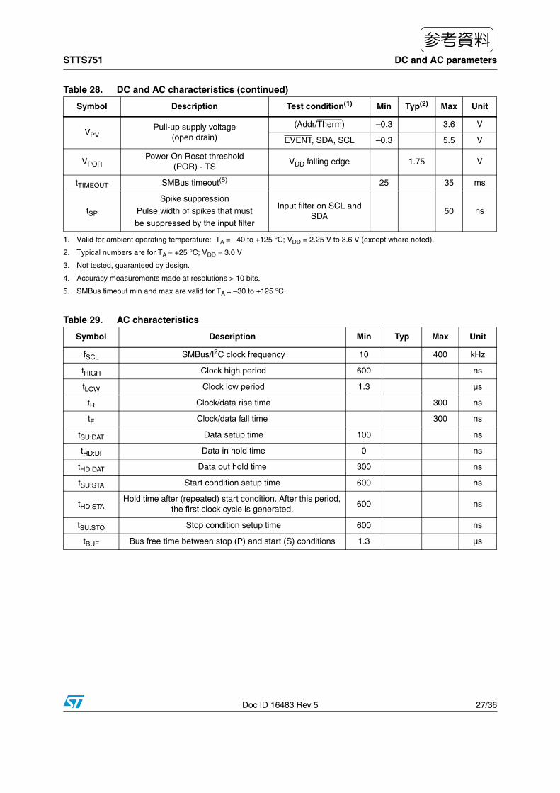
Table 28. DC and AC characteristics
Symbol Description Test condition(1) Min Typ(2) Max Unit
VDD Supply voltage 2.25 3.6 V
IDDOperating current dependent upon
conversion rate
0.0625 conversions/second(3) 15 35 µA
1 conversion/second(3) 20 40 µA
8 conversions/second 50 85 µA
32 conversions/second 125 250 µA
ISB Standby current 3 8 µA
Temperature measurement
Accuracy(4) 2.25 V to 3.6 V 0 °C to 85 °C ±1.0 ±1.5 °C
–40 °C to +125 °C ±2.0 ±2.5 °C
ResolutionSTTS751 is programmable from 9 bits to 12 bits (0.5 °C/LSB to 0.0625 °C)
9-bittemperature data
0.5 °C/LSB
9 bits
10-bit temperature data
(default)
0.25 °C/LSB
10 bits
11-bit temperature data0.125 °C/LSB
11 bits
12-bit temperature data0.0625 °C/LSB
12 bits
tCONV Conversion time
9-bit 10.5 14 ms
10-bit (default) 21 28 ms
11-bit 42 56 ms
12-bit 84 112 ms
VOLLow level output voltage
Addr/Therm, EVENT IOL = 4 mA 0.4 V
IOHHigh level output leakage current
EVENT, SDA, Addr/ThermVOH = VDD 1 µA
SMBus interface inputs (SDA, SCL)
VIH Input logic high (SCL, SDA) 2.3 V ≤ VDD ≤ 3.6 V0.7 x VDD
V
VIL Input logic low (SCL, SDA) 2.3 V ≤ VDD ≤ 3.6 V0.3 x VDD
V
IHI Logical "1" input current 0 V ≤ VIN ≤ VDD –1 1 µA
ILI Logical "0" input current 0 V ≤ VIN ≤ VDD –1 1 µA
CIN Input capacitance (SDA) 5 pF
ISINK SMBus output low sink current SDA forced to 0.6 V 6 mA
参考資料
STTS751 DC and AC parameters
Doc ID 16483 Rev 5 27/36
VPVPull-up supply voltage
(open drain)
(Addr/Therm) –0.3 3.6 V
EVENT, SDA, SCL –0.3 5.5 V
VPORPower On Reset threshold
(POR) - TSVDD falling edge 1.75 V
tTIMEOUT SMBus timeout(5) 25 35 ms
tSP
Spike suppression
Pulse width of spikes that mustbe suppressed by the input filter
Input filter on SCL and SDA
50 ns
1. Valid for ambient operating temperature: TA = –40 to +125 °C; VDD = 2.25 V to 3.6 V (except where noted).
2. Typical numbers are for TA = +25 °C; VDD = 3.0 V
3. Not tested, guaranteed by design.
4. Accuracy measurements made at resolutions > 10 bits.
5. SMBus timeout min and max are valid for TA = –30 to +125 °C.
Table 28. DC and AC characteristics (continued)
Symbol Description Test condition(1) Min Typ(2) Max Unit
Table 29. AC characteristics
Symbol Description Min Typ Max Unit
fSCL SMBus/I2C clock frequency 10 400 kHz
tHIGH Clock high period 600 ns
tLOW Clock low period 1.3 µs
tR Clock/data rise time 300 ns
tF Clock/data fall time 300 ns
tSU:DAT Data setup time 100 ns
tHD:DI Data in hold time 0 ns
tHD:DAT Data out hold time 300 ns
tSU:STA Start condition setup time 600 ns
tHD:STAHold time after (repeated) start condition. After this period,
the first clock cycle is generated. 600 ns
tSU:STO Stop condition setup time 600 ns
tBUF Bus free time between stop (P) and start (S) conditions 1.3 µs
参考資料

Package mechanical data STTS751
28/36 Doc ID 16483 Rev 5
9 Package mechanical data
In order to meet environmental requirements, ST offers these devices in different grades of ECOPACK® packages, depending on their level of environmental compliance. ECOPACK® specifications, grade definitions and product status are available at: www.st.com. ECOPACK® is an ST trademark.
参考資料

STTS751 Package mechanical data
Doc ID 16483 Rev 5 29/36
Figure 9. UDFN-6L (2 mm x 2 mm x 0.5 mm) package mechanical drawing
Table 30. UDFN-6L (2 mm x 2 mm x 0.5 mm) package mechanical data
Symmm inches
Min Typ Max Min Typ Max
A 0.45 0.50 0.55 0.018 0.020 0.022
A1 0.00 0.05 0.000 0.002
A3 0.065 0.003
b 0.20 0.25 0.30 0.008 0.010 0.012
D 1.95 2.00 2.05 0.077 0.079 0.081
E 1.95 2.00 2.05 0.077 0.079 0.081
e 0.65 0.026
L 0.50 0.60 0.70 0.020 0.024 0.028
8187820_A
参考資料

Package mechanical data STTS751
30/36 Doc ID 16483 Rev 5
Figure 10. SOT23-6L (2.90 mm x 2.80 mm) package mechanical drawing
Table 31. SOT23-6L (2.90 mm x 2.80 mm) package mechanical data
Symmm inches
Min Typ Max Min Typ Max
A 1.45 0.057
A1 0.00 0.15 0.000 0.006
A2 0.90 1.15 1.30 0.035 0.045 0.051
b 0.30 0.50 0.012 0.020
c 0.08 0.22 0.003 0.009
D 2.90 0.114
E 2.80 0.110
E1 1.60 0.063
e 0.95 0.037
e1 1.90 0.075
L 0.30 0.45 0.60 0.012 0.018 0.024
θ 0° 4° 8° 0° 4° 8°
N 6 6
7049717_G
参考資料

STTS751 Package mechanical data
Doc ID 16483 Rev 5 31/36
Figure 11. UDFN-6L package footprint
Figure 12. SOT23-6L package footprint
8187820_A(LP)
7049714_G(LP)
参考資料

Package mechanical data STTS751
32/36 Doc ID 16483 Rev 5
Figure 13. Carrier tape for UDFN-6L and SOT23-6L packages
T
K0
P1
A0
B0
P2
P0
CENTER LINESOF CAVITY
W
E
F
D
TOP COVERTAPE
USER DIRECTION OF FEEDAM03073v1
Table 32. Carrier tape dimensions for UDFN-6L and SOT23-6L packages
Package W D E P0 P2 F A0 B0 K0 P1 T Unit
UDFN-6L8.00
±0.30
1.50+0.10/–0.00
1.75±0.10
4.00±0.10
2.00±0.05
3.50±0.05
2.20±0.10
2.20±0.10
0.75±0.10
4.00±0.10
0.25±0.05
mm
SOT23-6L8.00
+0.30/–0.10
1.50+0.10/–0.00
1.75±0.10
4.00±0.10
2.00±0.10
3.50±0.05
3.23±0.10
3.17±0.10
1.37±0.10
4.00±0.10
0.254±0.013
mm
参考資料

STTS751 Package mechanical data
Doc ID 16483 Rev 5 33/36
Figure 14. Reel schematic
Note: The dimensions given in Table 33 incorporate tolerances that cover all variations on critical parameters.
A
D
B
Full radius
Tape slot In core for
Tape start 2.5mm min.width
G measured
At hub
C
N
40mm min.
Access hole
At slot location
T
AM04928v1
Table 33. Reel dimensions for 8 mm carrier tape - UDFN-6L and SOT23-6L packages
A
(max)
B
(min)C
D
(min)
N
(min)G
T
(max)
180 mm
(7 inch)1.5 mm
13 mm± 0.2 mm
20.2 mm 60 mm8.4 mm
+ 2/–0 mm14.4 mm
参考資料

Part numbering STTS751
34/36 Doc ID 16483 Rev 5
10 Part numbering
Table 34. Ordering information scheme
For other options, or for more information on any aspect of this device, please contact the ST sales office nearest you.
Example: STTS751-0 DP 3 F
Device type
STTS751-0
STTS751-1
Package
DP = UDFN-6L
WB = SOT23-6L
Temperature range
3 = –40 °C to 125 °C
Shipping method
F = ECOPACK® package, tape & reel
E = ECOPACK® package, tubes
参考資料

STTS751 Revision history
Doc ID 16483 Rev 5 35/36
11 Revision history
Table 35. Document revision history
Date Revision Changes
06-Nov-2009 1 Initial release.
21-Jan-2010 2
Updated Features; removed Therm2 throughout document (from Section 1, 2, 3.8, 4.6, 4.10, 5, Figure 1, 2, 3, 4, 6, Table 2, 3, 15, 28); updated Figure 3, Section 3.4, Section 4.6, Section 4.8, Section 4.10, Table 10, 11, 12, 13, 14, 15, 17, 18, 19, 20, 21, 22, 23, 24, 25; added package footprints (Figure 11 and 12); minor textual changes.
12-May-2010 3
Updated Section 3.7, Section 4.11, Section 5; Figure 6, 7, 11, 12; Table 3, 9, 25, 28, Table 31; added tape and reel information (Figure 13, 14 and Table 32, 33); minor textual changes in title and document.
01-Jul-2010 4Document status upgraded to full datasheet; updated cover page; added footnote to Table 28; minor textual changes.
20-Jul-2010 5 Removed footnote from Table 28.
参考資料

STTS751
36/36 Doc ID 16483 Rev 5
Please Read Carefully:
Information in this document is provided solely in connection with ST products. STMicroelectronics NV and its subsidiaries (“ST”) reserve theright to make changes, corrections, modifications or improvements, to this document, and the products and services described herein at anytime, without notice.
All ST products are sold pursuant to ST’s terms and conditions of sale.
Purchasers are solely responsible for the choice, selection and use of the ST products and services described herein, and ST assumes noliability whatsoever relating to the choice, selection or use of the ST products and services described herein.
No license, express or implied, by estoppel or otherwise, to any intellectual property rights is granted under this document. If any part of thisdocument refers to any third party products or services it shall not be deemed a license grant by ST for the use of such third party productsor services, or any intellectual property contained therein or considered as a warranty covering the use in any manner whatsoever of suchthird party products or services or any intellectual property contained therein.
UNLESS OTHERWISE SET FORTH IN ST’S TERMS AND CONDITIONS OF SALE ST DISCLAIMS ANY EXPRESS OR IMPLIEDWARRANTY WITH RESPECT TO THE USE AND/OR SALE OF ST PRODUCTS INCLUDING WITHOUT LIMITATION IMPLIEDWARRANTIES OF MERCHANTABILITY, FITNESS FOR A PARTICULAR PURPOSE (AND THEIR EQUIVALENTS UNDER THE LAWSOF ANY JURISDICTION), OR INFRINGEMENT OF ANY PATENT, COPYRIGHT OR OTHER INTELLECTUAL PROPERTY RIGHT.
UNLESS EXPRESSLY APPROVED IN WRITING BY AN AUTHORIZED ST REPRESENTATIVE, ST PRODUCTS ARE NOTRECOMMENDED, AUTHORIZED OR WARRANTED FOR USE IN MILITARY, AIR CRAFT, SPACE, LIFE SAVING, OR LIFE SUSTAININGAPPLICATIONS, NOR IN PRODUCTS OR SYSTEMS WHERE FAILURE OR MALFUNCTION MAY RESULT IN PERSONAL INJURY,DEATH, OR SEVERE PROPERTY OR ENVIRONMENTAL DAMAGE. ST PRODUCTS WHICH ARE NOT SPECIFIED AS "AUTOMOTIVEGRADE" MAY ONLY BE USED IN AUTOMOTIVE APPLICATIONS AT USER’S OWN RISK.
Resale of ST products with provisions different from the statements and/or technical features set forth in this document shall immediately voidany warranty granted by ST for the ST product or service described herein and shall not create or extend in any manner whatsoever, anyliability of ST.
ST and the ST logo are trademarks or registered trademarks of ST in various countries.
Information in this document supersedes and replaces all information previously supplied.
The ST logo is a registered trademark of STMicroelectronics. All other names are the property of their respective owners.
© 2010 STMicroelectronics - All rights reserved
STMicroelectronics group of companies
Australia - Belgium - Brazil - Canada - China - Czech Republic - Finland - France - Germany - Hong Kong - India - Israel - Italy - Japan - Malaysia - Malta - Morocco - Philippines - Singapore - Spain - Sweden - Switzerland - United Kingdom - United States of America
www.st.com
参考資料