2048 BIT STATIC MOS RAM WITH I/O PORTS AND TIMER
12
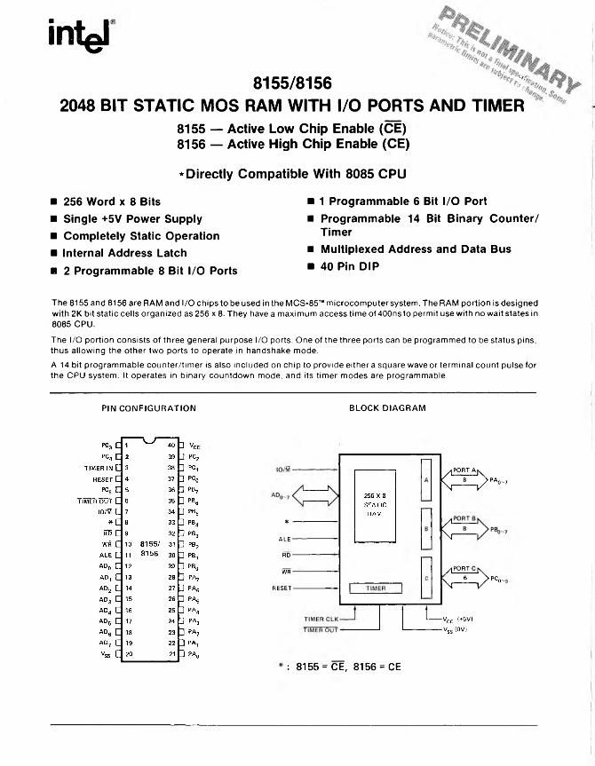
in y 8155/8156 ^ 2048 BIT STATIC MOS RAM WITH I/O PORTS AND TIMER 8155 — Active Low Chip Enable (CE) 8156 — Active High Chip Enable (CE) * Directly Compatible With 8085 CPU ■ 256 Word x 8 Bits ■ Single +5V Power Supply ■ Completely Static Operation ■ Internal Address Latch ■ 2 Programmable 8 Bit I/O Ports ■ 1 Programmable 6 Bit I/O Port ■ Programmable 14 Bit Binary Counter/ Timer ■ Multiplexed Address and Data Bus ■ 40 Pin DIP The 8155 and 8156 are RAM and I/O chips to be used in the MCS-85™ microcomputer system. The RAM portion is designed with 2K bit static cells organized as 256 x 8. They have a maximum access time of 400ns to permit use with no wait states in 8085 CPU. The I/O portion consists of three general purpose I/O ports. One of the three ports can be programmed to be status pins, thus allowing the other two ports to operate in handshake mode. A 14 bit programmable counter/timer is also included on chip to provide either a square wave or terminal count pulse for the CPU system. It operates in binary countdown mode, and its timer modes are programmable. PIN CONFIGURATION BLOCK DIAGRAM * - ALE- RD- WR- RESET- /1 P?.RTAK V V PV' Z1 V y lp ..?.RT_-K v-^>pc- t_. vcc (+5V) vss (0V) : 8155 = CE, 8156 = CE
Transcript of 2048 BIT STATIC MOS RAM WITH I/O PORTS AND TIMER
i n y
8155/8156 ^2048 BIT STATIC MOS RAM WITH I/O PORTS AND TIMER
8155 — Active Low Chip Enable (CE)8156 — Active High Chip Enable (CE)
* Directly Compatible With 8085 CPU
■ 256 Word x 8 Bits■ Single +5V Power Supply■ Completely Static Operation■ Internal Address Latch■ 2 Programmable 8 Bit I/O Ports
■ 1 Programmable 6 Bit I/O Port■ Programmable 14 Bit Binary Counter/
Timer■ Multiplexed Address and Data Bus■ 40 Pin DIP
The 8155 and 8156 are RAM and I/O chips to be used in the MCS-85™ microcomputer system. The RAM portion is designed with 2K bit static cells organized as 256 x 8. They have a maximum access time of 400ns to permit use with no wait states in 8085 CPU.
The I/O portion consists of three general purpose I/O ports. One of the three ports can be programmed to be status pins, thus allowing the other two ports to operate in handshake mode.A 14 bit programmable counter/timer is also included on chip to provide either a square wave or terminal count pulse for the CPU system. It operates in binary countdown mode, and its timer modes are programmable.
PIN CONFIGURATION BLOCK DIAGRAM
* -
A L E -
R D -
W R -
R E SET-
/1 P?.RTAKV V PV'
Z1V
y lp..?.RT_-K
v - ^ > pc-
t _ . vcc (+5V) vss (0V)
: 8155 = CE, 8156 = CE

8155/8156
8155/8156 FUNCTIONAL PIN DEFINITIONThe following describes the functions of all of the 8155/8156 pins.
Symbol
RESET
ADq_7
CE or CE
RD
WR
ALE
IO/M
Function
The Reset signal is a pulse provided by the 8085 to initialize the system. Input high on this line resets the chip and initializes the three I/O ports to input mode. The width of RESET pulse should typically be 600 nsec. (Two 8085 clock cycle times).These are 3-state Address/Data lines that interface with the CPU lower 8- bit Address/Data Bus. The 8-bit address is latched into the address latch on the falling edge of the ALE. The address can be either for the memory section or the I/O section depending on the polarity of the IO/M input signal. The 8-bit data is either written into the chip or Read from the chip depending on the status of WRITE or READ input signal.Chip Enable: On the 8155. this pin is CE and is ACTIVE LOW. On the 8156. this pin is CE and is ACTIVE HIGH.Input low on this line with the Chip Enable active enables the AD0-7 buffers. If SO/M pin is low, the RAM content will be read out to the AD bus. Otherwise the content of the selected I/O port will be read to the AD bus.Input low on this line with the Chip Enable active causes the data on the AD lines to be written to the RAM or l/0_ports depending on the polarity of IO/M.
Address Latch Enable: This control signal latches both the address on the AD0-7 lines and_the state of the Chip Enable and IO/M into the chip at the falling edge of ALE.IO/Memory Select: This line selects the memory if low and selects the IO if high.
Symbol
PA0-7(8)
PB0_7(8)
PC 0-5 (6)
TIMER IN TIMER OUT
VCC
V SS
Function
These 8 pins are general purpose I/O pins. The in/out direction is selected by programming the Command/ Status Register.These 8 pins are general purpose I/O pins. The in/out direction is selected by programming the Command/ Status Register.These 6 pins can function as either input port, output port, or as control signals for PA and PB. Programming is done through the C/S Register. When PC0-5 are used as control signals, they will provide the following:
PCO — A INTR (Port A Interrupt)PC1 — ABF (Port A Buffer full)PC2 — A STB (Port A Strobe)PCS — B INTR (Port B Interrupt)PC4 ~ B BF (Port B Buffer Full)PC5 — B STB (Port B Strobe)This is the input to the counter timer.This pin is the timer output. This output can be either a square wave or a pulse depending on thetimer mode.
+5 volt supply.
Ground Reference.

8155/8156
OPERATIONAL DESCRIPTIONThe 8155/8156 includes the following operational features:
• 2K Bit Static RAM organized as 256 x 8• Two 8-bit I/O ports (PA & PB) and one 6-bit I/O port
(PC)• 14-bit binary down counter
The I/O portion contains four registers (Command/ Status, PAo-7, PBq-7, PCq-5). The IO/M (lO/Memory Select) pin selects the I/O or the memory (RAM) portion. Detailed descriptions of memory, I/O ports and timer functions will follow.
The 8-b^address on the AD lines, the Chip Enable input, and IO/M are all jatched on chip at the falling edgeof ALE. A low on the IO/M must be provided to select the memory section.
CE (8155)
OR
CE (8156 ) y// ' A __
............. - - ...............
k VIO /M / \ .
>------ <X
©D<
ADDRESS
ALE y A JR D O R W R V _ ________________/
NOTE: FOR D E TA ILE D T IM IN G D IA G R A M IN FO R M A TIO N , SEE F IGURE 7 AND A.C. CHARACTERISTICS.
FIGURE 1. MEMORY READ/WRITE CYCLE.

8155/8156
PROGRAMMING OF THE COMMAND/ STATUS REGISTERThe command register consists of eight latches one for each bit. Four bits (0-3) define the mode of the ports, two bits (4-5) enable or disable the interrupt from port C when it acts as control port, and the last two bits (6-7) are for the timer.The C/S register contents can be altered at any time by using the I/O address XXXXX000 during a WRITE operation. The meaning of each bit of the command byte is defined as follows:
READING THE COMMAND/STATUS REGISTERThe status register consists of seven latches one for each bit; six (0-5) for the status of the ports and one (6) for the status of the timer.The status of the timer and the I/O section can be polled by reading the C/S Register (Address XXXXX000). Status word format is shown below:
7 6 5 4 3 2 1 0
AD7 ADg AD5 AD4 AD3 AD2 AD-J ADq
j t e | b I in t r IIN TE l A IlNTR B BF B A BF AIEE
r PORT A INTERRUPT REQUEST
PORT A BUFFER FULL/EMPTY (INPUT/OUTPUT)
PORT A INTERRUPT ENABLE
PORT B INTERRUPT REQUEST
PORT B BUFFER FULL/EMPTY (INPUT/OUTPUT)
PORT B INTERRUPT ENABLED
TIMER INTERRUPT (THIS BIT IS LATCHED HIGH WHEN TERMINAL COUNT IS REACHED, AND IS RESET TO LOW UPON READING OF THE C/S REGISTER OR STARTING NEW COUNT.)
FIGURE 2. COMMAND/STATUS REGISTER BIT ASSIGNMENT.
FIGURE 3. COMMAND/STATUS REGISTER STATUS WORD FORMAT.

8155/8156
INPUT/OUTPUT SECTIONThe I/O section of the 8155/8156 consists of four registers as described below.
The following diagram shows how I/O PORTS Aand Bare structured within the 8155 and 8156:
8155/8156ONE BIT OF PORT A OR PORT B
• Command/Status Register (C/S) — This register is assigned the address XXXXX000. The C/S address serves the dual purpose.When the C/S register is selected during WRITE operation, a command is written into the command register. The contents of this register are not accessible through the pins.When the C/S (XXXXX000) is selected during a READ operation, the status information of the I/O ports and the timer become available on the AD0-7 lines.
• PA Register — This register can be programmed to be either input or output ports depending on the status of the contents of the C/S Register. Also depending on the command, this port can operate in either the basic mode or the strobed mode (See timing diagram). The I/O pins assigned in relation to this register are PA0-7. The address of this register is XXXXX001.
NOTES:(1) OUTPUT MODE(2) SIMPLE INPUT(3) STROBED INPUT
MULTIPLEXERCONTROL
(4) = 1 FOR OUTPUT MODE = 0 FOR INPUT MODE
READ PORT = (IO /M j1) • (RJDjO) • (CE ACTIVE)* (PORT ADDRESS SELECTED) WRITE PORT = (IO/M=1) • (WR=Q) • (CE ACTIVE) • (PORT ADDRESS SELECTED)
• PB Register — This register functions the same as PA Register. The I/O pins assigned are PB0_7. The address of this register is XXXXX010.
• PC Register — This register has the address XXXXX011 and contains only 6-bits. The 6-bits can be programmed to be either input ports, output ports or as control signals for PA and PB by properly programming the AD2 and AD3 bits of the C/S register.When PC0-5 is used as a control port, 3-bits are assigned for Port A and 3 for Port B. The first bit is an interrupt that the 8155 sends out. The second is an output signal indicating whether the buffer is full or empty, and the third is an input pin to accept a strobe for the strobed input mode. See Table 1.
When the ‘C’ port is programmed to either ALT3 or AL.T4, the control signals for PA and PB are initialized as follows:
CONTROL INPUT MODE OUTPUT MODEBF
INTRSTB
LowLow
Input Control
LowHigh
Input Control
Note in the diagram that when the I/O ports are programmed to be output ports, the contents of the output ports can still be read by a READ operation when appropriately addressed.Note also that the output latch is cleared when the port enters the input mode. The output latch cannot be loaded by writing to the port if the port is in the input mode. The result is that each time a port mode is changed from input to output, the output pins will go low. When the 8155/56 is RESET, the output latches are all cleared and all 3 ports enter the input mode.When in the ALT 1 or ALT 2 modes, the bits of PORT C are structured like the diagram above in the simple input or output mode, respectively.Reading from an input port with nothing connected to the pins will provide unpredictable results.
TABLE 1. TABLE OF PORT CONTROL ASSIGNMENT.Pin ALT 1 ALT 2 ALT 3 ALT 4PCO In p u t P ort O u tp u t P ort A IN TR (P ort A In te rru p t) A IN TR (P o rt A In te rru p t)PC1 in p u t P ort O u tp u t P o rt A BF (P o rt A B u ffe r Fu ll) A BF (P o rt A B u ffe r Fu ll)PC2 In p u t P ort O u tp u t P ort A S TB (P o rt A S trob e ) A S TB (P o rt A S trob e )PC3 In p u t P ort O u tp u t P ort O u tp u t P ort B IN TR (P o rt B In te rru p t)PC4 In p u t P ort O u tp u t P ort O u tp u t P ort B BF (P o rt B B u ffe r Full).PC5 In p u t P ort O u tp u t P ort O u tp u t P ort B S TB (P o rt B S trob e )
The set and reset of INTR and BF with respect to STB, WR and RD timing is shown in Figure 8.
To summarize, the registers’ assignments are: Address Pinouts Functions No. of Bits
x x x x x o o o In te rn a l C o m m a n d /S ta tu s R e g is te r 8XXXXX001 PAO-7 G e n e ra l P u rp o s e I /O P o rt 8XXXXX010 PBO-7 G e n e ra l P u rp o s e I /O P o rt 8XXXXX011 PCO-5 G e n e ra l P u rp o s e I /O P o rt o r
C o n tro l L in e s6

8155/8156
TIMER SECTIONThe timer is a 14-bit counter that counts the ‘timer input’ pulses and provides either a square wave or pulse when terminal count (TC) is reached.The timer has the I/O address XXXXX100 for the low order byte of the register and the I/O address XXXXX101 for the high order byte of the register.The timer addresses serve a dual purpose. During WRITE operation, a COUNT LENGTH REGISTER (CLR) with a count length (bits 0-13) and a timer mode (bits 14-15) are loaded. During READ operation the contents of the counter (the present count) and the mode bits are read.To be sure that the right content of the counter is read, it is preferable to stop counting, read it, and then load it again and continue counting.To program the timer, the COUNT LENGTH REG is loaded first, one byte at a time, by selecting the timer addresses. Bits 0-13 will specify the length of the next count and bits 14-15 will specify the timer output mode.There are four modes to choose from:
0. Puts out low during second half of count.1. Square wave2. Single pulse upon TC being reached3. Repetitive single pulse everytime TC is readied and automatic reload of counter upon TC being reached, until instructed to stop by a new command loaded into C/S.
Bits 6-7 of Command/Status Register Contents are used to start and stop the counter. There are four commands to choose from:
Note: See the further description on Command/Status Register.
m 2 Mi T13 Tl2 T i i T 10 T 9 t 8
I___________II________ _ JITIMER MODE MSB OF CNT LENGTH
t 7 t 6 t 5 t 4 t 3 t 2 T 1 To
I______________________________________ _________I
LSB OF CNT LENGTH
FIGURE 4. TIMER FORMAT
M2 Ml defines the timer mode as follows:
M2 M1
0 0 Puts out low during second half ofcount.
0 1 Square wave, i.e., the period of thesquare wave equals the count length programmed with automatic reload at terminal count.
1 0 Single pulse upon TC beingreached.
1 1 Automatic reload, i.e., single pulseeverytime TC is reached.
Note: In case of an asymmetric count, i.e. 9, larger half o f the count w ill be high, the larger count w ill stay active as shown in Figure 5.
C/S7 C/S6
0 0 NOP — Do not affect counter operation.0 1 STOP — NOP if timer has not started; stop
counting if the timer is running.1 0 STOP AFTER TC — Stop immediately after
present TC is reached (NOP if timer has not started)
1 1 START - - Load mode and CNT length and start immediately after loading (if timer isnot presently running). If timer is running, start the new mode and CNT length immediately after present TC is reached.
I
Note: 5 and 4 refer to the number o f clock cycles in that time period.
FIGURE 5. ASYMMETRIC COUNT.
The timer in the 8155 is not initialized to any particular mode when hardware RESET occurs, but RESET does stop the counting. Therefore, counting cannot begin following RESET until the desired mode and count length and START command are issued.

8155/8156
8085 MINIMUM SYSTEM CONFIGURATIONFigure 6shows that a minimum system is possible using only three chips:
• 256 Bytes RAM• 2K Bytes ROM• 38 I/O Pins• 1 Interval Timer• 4 Interrupt Levels
FIGURE 6. 8085 MINIMUM SYSTEM CONFIGURATION.

8155/8156
ABSOLUTE MAXIMUM RATINGS*
Temperature Under Bias ........................... 0°Cto+70°CStorage Temperature ......................... -65°Cto +150°CVoltage on Any Pin
With Respect to Ground ......................... -0.3Vto+7VPower Dissipation .................................................. 1.5W
*COMMENT: Stresses above those listed under "Absolute, Maximum Ratings" may cause permanent damage to the device. This is a stress rating only and functional operation o f the device at these or any other conditions above those indicated in the operational sections o f this specification is not implied. Exposure to absolute maximum rating conditions for extended periods may affect device reliability.
D.C. CHARACTERISTICS (ta = o°c to 70°C; vcc = 5V ± 5%)
SYMBOL PARAMETER MIN. MAX. UNITS TEST CONDITIONS
V|L Input Low Voltage -0.5 0.8 V
VIH Input High Voltage 2.0 V
V0 L Output Low Voltage 0.45 V Iq l = 2mA
VOH Output High Voltage 2.4 V Iqh = -400juA
IlL Input Leakage 10 pA v in = V c c to ov
•lo Output Leakage Current ±10 pA 0.45V < V 0UT < V Cc
>cc Vcc Supply Current 180 mA
8155/8156
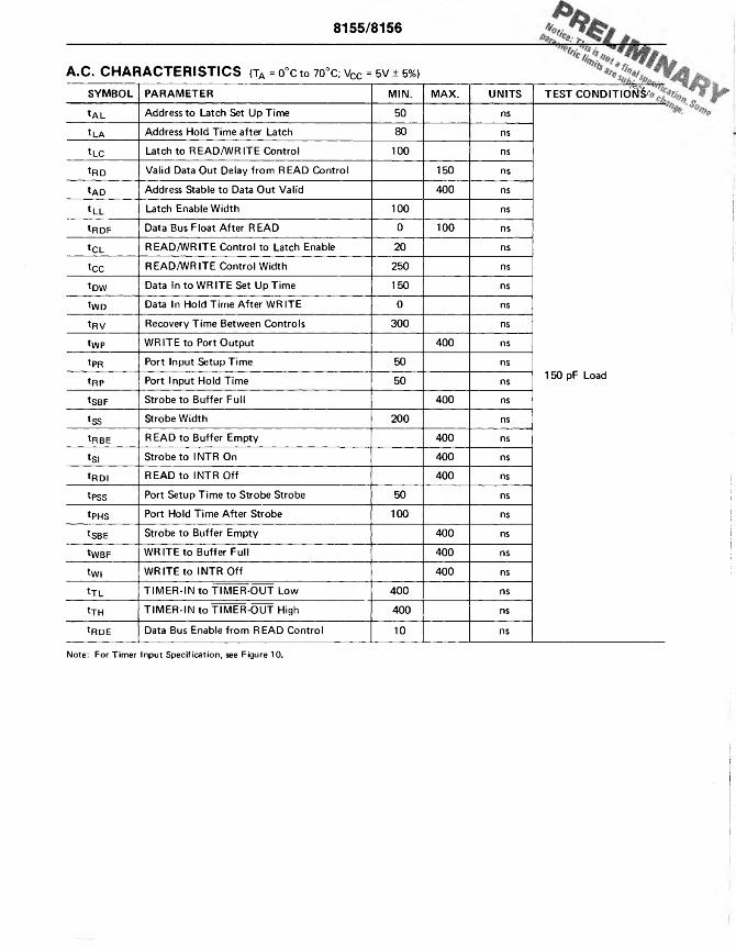
A.C. CHARACTERISTICS (ta = o°cto 70°C; vCc = 5V + 5%)
SYMBOL PARAMETER MIN. MAX. UNITS
*AL Address to Latch Set Up Time 50 ns
*LA Address Hold Time after Latch 80 ns
tLC Latch to READ/WRITE Control 100 ns
tRD Valid Data Out Delay from READ Control 150 ns
^AD Address Stable to Data Out Valid 400 ns
tLL Latch Enable Width 100 ns
*RDF Data Bus Float After READ 0 100 ns
tCL READ/WRITE Control to Latch Enable 20 ns
tcc READ/WRITE Control Width 250 ns
*DW Data In to WRITE Set Up Time 150 ns
*WD Data In Hold Time After WRITE 0 ns
*RV Recovery Time Between Controls 300 ns
tWp WRITE to Port Output 400 ns
tpR Port Input Setup Time 50 ns
tRP Port Input Hold Time 50 ns
*SBF Strobe to Buffer Full 400 ns
tss Strobe Width 200 ns
tRBE READ to Buffer Empty 400 ns
tsi Strobe to INTR On 400 ns
tRDI READ to INTR Off 400 ns
tpss Port Setup Time to Strobe Strobe 50 ns
tPHS Port Hold Time After Strobe 100 ns
tSBE Strobe to Buffer Empty 400 ns
tWBF WRITE to Buffer Full 400 ns
twi WRITE to INTR Off 400 ns
tTL TIMER-IN to TIMER-OUT Low 400 ns
tTH TIMER-IN to TIMER-OUT High 400 ns
tRDE Data Bus Enable from READ Control 10 ns
------
TEST CONDITlditffo
150 pF Load
Note: For Timer Input Specification, see Figure 10.

8155/8156
B. WRITE CYCLE
FIGURE 7. 8155/8156 READ/WRITE TIMING DIAGRAMS

8155/8156W M
W fl
A. STROBED INPUT MODE
B. STROBED OUTPUT MODE
FIGURE 8. STROBED I/O TIMING.

8155/8156
A. BASIC INPUT MODE
RD
t PR----
k ___________________ 7l
INPUT ^.̂.... ....—... ........................ ............—
B. BASIC OUTPUT MODE
FIGURE 9. BASIC I/O TIMING WAVEFORM.
LOAD . RELOADCOUNTER COUNTER — ►FROM CLR ' FROM CLR '
COUNT| 0 | 3 | 2 | 1 | 0 | 3 | 2
COUNTDOWN FROM 3 TO 0
tCYC 320 ns MIN.
W e & Vall 30 ns MAX- t 1 80 ns MIN.t2 120 ns MIN.tJL TIMER-IN TO TIMER-OUT LOW (TO BE DEFINED).tTH TIMER-IN TO TIMER-OUT HIGH (TO BE DEFINED).
FIGURE 10. TIMER OUTPUT WAVEFORM.