
2019 NEPP ETW: RF Driven Lifetesting of GaN Power MMICs · 2 Statement of the Problem the...
16
1 © 2019The Aerospace Corporation RF Driven Lifetesting of GaN Power MMICs John Scarpulla, Chris Clark, Albert Young and Yat Chan 19 June, 2019 NASA NEPP Conference Beltsville , MD
Transcript of 2019 NEPP ETW: RF Driven Lifetesting of GaN Power MMICs · 2 Statement of the Problem the...

1© 2019The Aerospace Corporation
RF Driven Lifetesting of GaN Power MMICs
John Scarpulla, Chris Clark, Albert Young and Yat Chan
19 June, 2019NASA NEPP Conference
Beltsville, MD
2
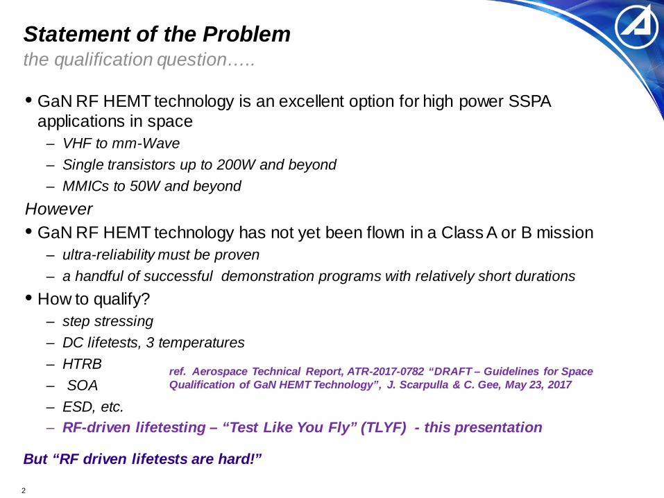
Statement of the Problemthe qualification question…..
But “RF driven lifetests are hard!”
• GaN RF HEMT technology is an excellent option for high power SSPA applications in space
– VHF to mm-Wave– Single transistors up to 200W and beyond– MMICs to 50W and beyond
However• GaN RF HEMT technology has not yet been flown in a Class A or B mission
– ultra-reliability must be proven– a handful of successful demonstration programs with relatively short durations
• How to qualify? – step stressing– DC lifetests, 3 temperatures– HTRB– SOA– ESD, etc.– RF-driven lifetesting – “Test Like You Fly” (TLYF) - this presentation
ref. Aerospace Technical Report, ATR-2017-0782 “DRAFT – Guidelines for Space Qualification of GaN HEMT Technology”, J. Scarpulla & C. Gee, May 23, 2017

3
Traditional lifetests might miss “sneak” failure modelow EA mechanism(s) must be disproven
TLYF testing recommended to confirm high reliability
350 300 250 200 150 125°C
15 years
5
1
Traditional lifetests
typical mission durations
actual RF power amp usage
“sneak” failure mode
1.8 eV 1.0
0.2

4
Flight-like Test Article TLYF details
test goals: 4 DUTs tested for 5000 hours
• Custom broadband MMIC power amp– 0.25µm gate length HEMTs process– Output Power 41dBm (12.5W) min.
• at 6dB compression• at pulsed duty cycle ≤ 50%• at Tch = 200°C
– Power-added efficiency 40%– Drain voltage VDD = 40V– Drain Current, Quiescent IDQ =480 mA– bandwidth 150MHz – 2GHz– devices packaged in ceramic packages– removable lids
• Success Criteria (in-situ)– output power degradation, Δ Pout < 1 dB– small signal gain degradation, Δ s21 < 1dB– current at ID = 860 mA, IG < 1mA/mm
• Burn-in– T = 200°C channel, 320 hours– DC only, VDD = 40V, IDQ =0.48 A– N2 purged
• pre/post measurements– swept s-parameters– Pout vs. Pin at 1.5 GHz– pulsed IV
• TLYF test– defined pulsed waveform– Pout ~ 41 dBm– Pin ~ 10 dBm– T = 50°C baseplate, (est. 200°C channel)– lab air environment– ID = 860 mA, pulsed– in-situ measurements of
• gain (s21), Pout, IG gate current

5
RF stress waveforms for TLYFpulsed operation to simulate mission
– RF input has a 50% duty cycle: 50msec on / 50 msec off f = 1.5 GHz– Maintain pulsed RF input for 20 minutes on period– Then RF input and VDD are switched off for 5 min. rest period
• s21 measurement at f=1.5GHz during each off period– Repeat the sequence for up to 5,000 hours
– Risetimes and falltimes of RF pulses = 1µsec– VDD and VG on/off risetime and falltime = 50µsec
Pulsed RF: 50msec on / 50msec off, f = 1.5GHz
RF Output
VDD
20 min5 min.
~+40dBm
40V0V
timein-situ s21 measurements
simultaneous pulsed VDD

6
TLYF Essential Requirementstest set design features
Special measures have been taken to protect the GaN DUTs
• continuous measurement of Pout, ID, IG, VD, VG– once per second, data stored
• Protections (very important)• Substantial VDD power supply can potentially do serious damage
– GaN HEMT’s are very susceptible to damage from improper DC biasing• Rapidly (within µ seconds) remove prime VDD power IF:
– VG gate bias is lost, • protects device from catastrophic destruction in case of a gate short failure• gate short could be a dendrite, a weak spot in field plate, MIMCAP failure etc.
– IG gate currtent rises above acceptable limit (> 1mA/mm)• possible indication of imminent failure• hot electron degradation or trap generation at drain-gate recess
– drain overcurrent, ID• protects device from catastrophic destruction in case a drain-source short develops
• In case bad things happen, the DUT does not suffer collateral damage– DUT failure analysis can be performed

7
MMIC test set block diagramdetects three fault types that rapidly latch the DUT off
Luckily the protection circuits were only invoked in cases of operator error – no test failure conditions were detected

8
Test Set
Custom test set developed for unattended continuous operation
4 DUTs in modified Accel-RFfixtures mounted on cold plate
drain power suppliesLabView
software
Instruments:spectrum analyzer,RF switches, oscilloscope,pulser, RF source
protection circuits
voltage/current meters

9
Pulse Schemestaggering of pulses to reduce noise

10
∆Pout is within ± 0.2 dB for 2450 hours, success criterion is ± 1 dB
Pout
in-situ Results

11
∆s21 is within ± 0.5 dB for 2450 hours, success criterion is ± 1 dB
s21
in-situ Results

12
|IG| < 22 µA (< 18.3 µA/mm) success criterion is < 1 mA/mm
IGin-situ Results

13
Ex-situ resultsgain and gain compression, at 0, 330 and 900 hrs (test still running)
small changes are insignificant and within instrument and configurational errors

14
Ex-situ resultsPulsed IV and transfer characteristic at 0, 330 and 900 hrs.
small changes are insignificant and within instrument and configurational errors

15
ConclusionsGaN RF-driven lifetest• A RF-driven lifetest system has been configured
– pulsed operation at 1.5GHz– special attention paid to protection of the devices in case of faults or failures– custom software– in situ measurements of key parameters of interest:
• output power, gain and gate current• a custom wideband GaN MMIC device has been tested under TLYF conditions
– tests have successfully run to ~2,500 hours– with goal to run to > 5,000 hours– output power, gain and gate current changed negligibly to ~2500 hours– goal is to run to 5,000 hours or longer
• qualification of the GaN device and fabrication process was enhanced – eliminates concerns about low EA mechanisms– low EA “sneak” mechanisms could be missed in traditional qual
• Lessons learned– implement an elapsed time counter– dry runs to simulate power shutdown, air conditioning failure ,etc.– rehearse the startup and shutdown– careful fixture design

16
Acronyms• HEMT high electron mobility transistor• DUT device under test• IV current (I) vs. voltage (V)• TLYF test like you fly• RF radio frequency• DC direct current• VHF very high frequency• HTRB high temperature reverse bias (stress test)• SOA safe operating area• ESD electrostatic discharge• mmW millimeter wave• MMIC monolithic microwave integrated circuit• EA activation energy• HPA high power amplifier• SSPA solid state power amplifier• GaN Gallium Nitride• IDQ drain current, quiescent point• VDD drain power supply voltage• Tch channel temperature• N2 nitrogen (gas)• RFOLT RF operational life test• Pout vs. Pin measurement and plot of output power vs. input power


