2017 Summer Camp day3 part2 - cl.cam.ac.uk · PDF file• Synopsys Design Constraints...
36
NetFPGA Summer Course Presented by: Andrew W Moore, Noa Zilberman, Gianni Antichi Stephen Ibanez, Marcin Wojcik, Jong Hun Han, Salvator Galea, Murali Ramanujam, Jingyun Zhang, Yuta Tokusashi University of Cambridge July 24 – July 28, 2017 http://NetFPGA.org
Transcript of 2017 Summer Camp day3 part2 - cl.cam.ac.uk · PDF file• Synopsys Design Constraints...

NetFPGA Summer Course
Presented by: Andrew W Moore, Noa Zilberman, Gianni AntichiStephen Ibanez, Marcin Wojcik, Jong Hun Han,
Salvator Galea, Murali Ramanujam, Jingyun Zhang, Yuta Tokusashi
University of CambridgeJuly 24 – July 28, 2017
http://NetFPGA.org

Summer Course Technion, Haifa, IL 2015 2
Finally, after hours of work you managed to finalise your HDL code and make it working in simulation!!!!

Summer Course Technion, Haifa, IL 2015 3
Once the bitfile is created you need to:
• Check if your design meet the timing.
• Debug your HW code if regression tests are not passed.

Summer Course Technion, Haifa, IL 2015 4
Once the bitfile is created you need to:
• Check if your design meet the timing.
• Debug your HW code if regression tests are not passed.

Static Timing Analysis (STA)
Summer Course Technion, Haifa, IL 2015 5
A design netlist is an interconnected set of ports, cells and nets

Static Timing Analysis (STA)
Summer Course Technion, Haifa, IL 2015 6
A design netlist is an interconnected set of ports, cells and nets
• The functionality of a design is determined by RTL code (verilog, vhdl, etc.) and verified by simulation tools

Static Timing Analysis (STA)
Summer Course Technion, Haifa, IL 2015 7
A design netlist is an interconnected set of ports, cells and nets
• The functionality of a design is determined by RTL code (verilog, vhdl, etc.) and verified by simulation tools
• The quality of your RTL determines how easy timing will be met
Static Timing Analysis (STA)
Summer Course Technion, Haifa, IL 2015 8
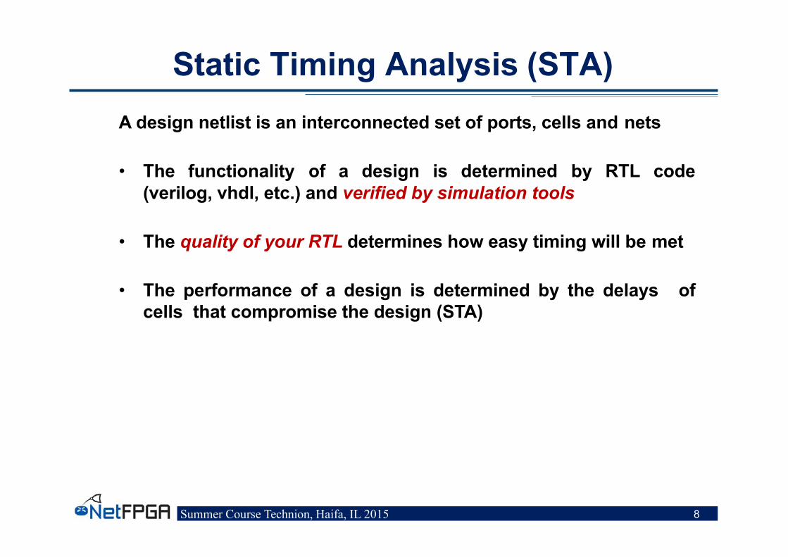
A design netlist is an interconnected set of ports, cells and nets
• The functionality of a design is determined by RTL code (verilog, vhdl, etc.) and verified by simulation tools
• The quality of your RTL determines how easy timing will be met
• The performance of a design is determined by the delays of cells that compromise the design (STA)

Static Timing Analysis (STA)
Summer Course Technion, Haifa, IL 2015 9
A design netlist is an interconnected set of ports, cells and nets
• The functionality of a design is determined by RTL code (verilog, vhdl, etc.) and verified by simulation tools
• The quality of your RTL determines how easy timing will be met
• The performance of a design is determined by the delays of cells that compromise the design (STA)
• Static timing analysis doesn’t check the functionality of the components but rather performance of components

STA GoalsMany FPGA processes are timing driven:- Synthesis for circuit construction- Placer for optimal cells locations- Router for choosing routing elements
Summer Course Technion, Haifa, IL 2015 10

STA GoalsMany FPGA processes are timing driven:- Synthesis for circuit construction- Placer for optimal cells locations- Router for choosing routing elements
Constraints are used to determine the desired performance goals
STA reports whether the design will provide the desired performance through reports
Summer Course Technion, Haifa, IL 2015 11

Component delays
Summer Course Technion, Haifa, IL 2015 12
Each component has delays to perform it function:- LUT has propagation delay from it’s ins to outs- Net has delay from driver to receiver- FF required stable data for a certain time around sampling point

Component delays
Summer Course Technion, Haifa, IL 2015 13
Each component has delays to perform it function:- LUT has propagation delay from it’s ins to outs- Net has delay from driver to receiver- FF required stable data for a certain time around sampling point
Delays are also dependent of environment factors. These aredetermined and characterized by Xilinx during device design.
Timing is extracted over the operating range of the device:- Process (different speed grades)- Voltage (min ® max)- Temperature (min ® max)

Static Timing Path- A static timing path is a path that starts at a clock element- Propagates through any # combinatorial elements and nets- Ends at clocking element
Source clock delay – starting top level clock port and ending at the launch FFData path delay – delay to the capturing FFDestination clock delay – there might be a difference bw these two FFs
Summer Course Technion, Haifa, IL 2015 14

Setup checkSetup Timing Check checks that data arrives in good time
Checks that change in a clocked element has time to propagate to other clocked elements before the next clock event
Simple case – same domain & only data path is considered:T(D1_CLK) + T(FF1(Clk->Q)) + T(Comb) < T (CLKperiod) – T(FF2(setup)) – T(SU) + T(D2_CLK)
Summer Course Technion, Haifa, IL 2015 15

Hold checkHold time checks that data doesn’t arrive too quickly
Checks DATA isn’t caught at destination FF at the same clock as the clock that launched it at source FF
Simple case – same domain & only data path is considered:T(D1_CLK) + T(FF1(Clk->Q)) + T(Comb) > T(FF2(hold)) + T(D2_CLK) + T(HU)
Summer Course Technion, Haifa, IL 2015 16

Constraints MethodologyDesign constraints define the requirements that must be met by the compilation flow in order for the design to be functional on the board
Summer Course Technion, Haifa, IL 2015 17

Constraints MethodologyDesign constraints define the requirements that must be met by the compilation flow in order for the design to be functional on the board
• Over-constraining and under-constraining is bad, so use reasonable constraints that correspond to your requirements
Summer Course Technion, Haifa, IL 2015 18
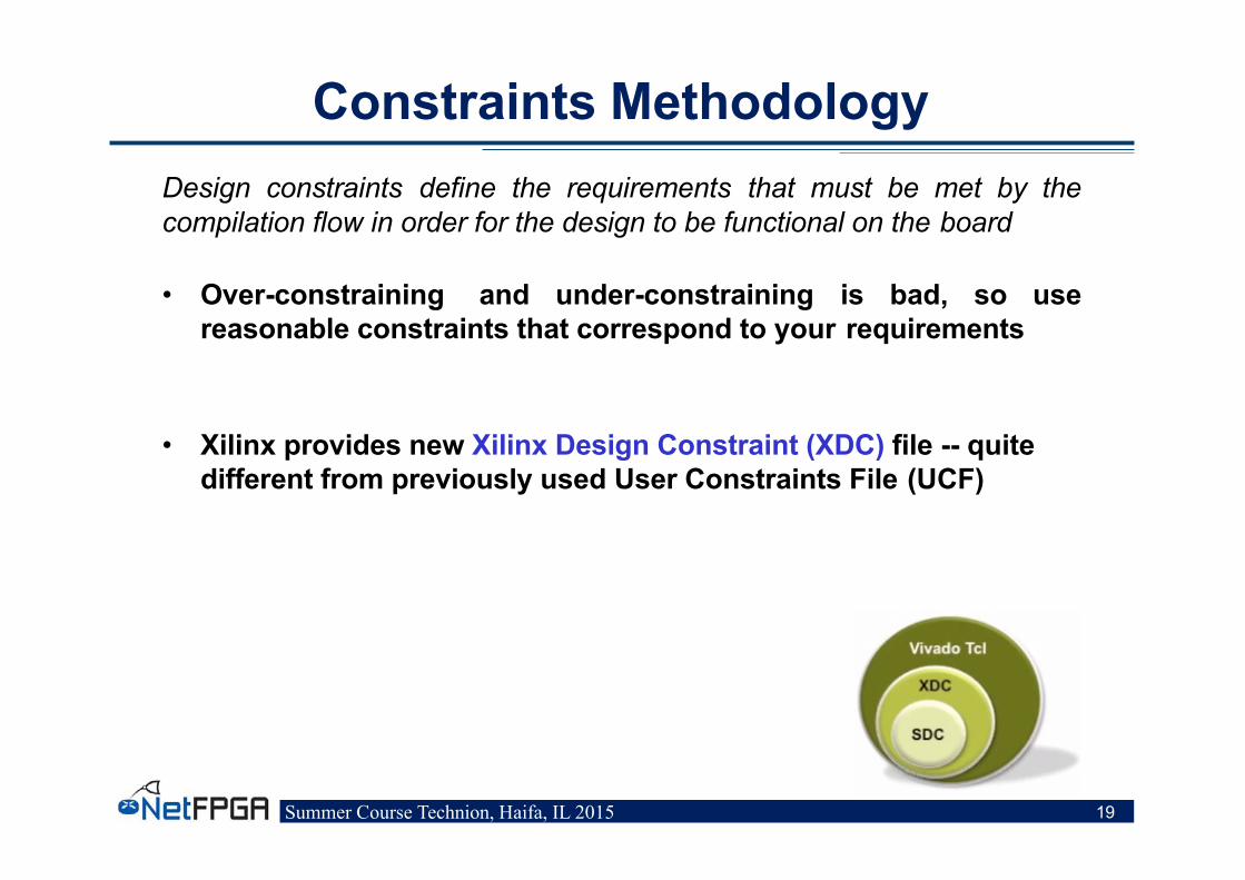
Constraints MethodologyDesign constraints define the requirements that must be met by the compilation flow in order for the design to be functional on the board
• Over-constraining and under-constraining is bad, so use reasonable constraints that correspond to your requirements
• Xilinx provides new Xilinx Design Constraint (XDC) file -- quite different from previously used User Constraints File (UCF)
Summer Course Technion, Haifa, IL 2015 19
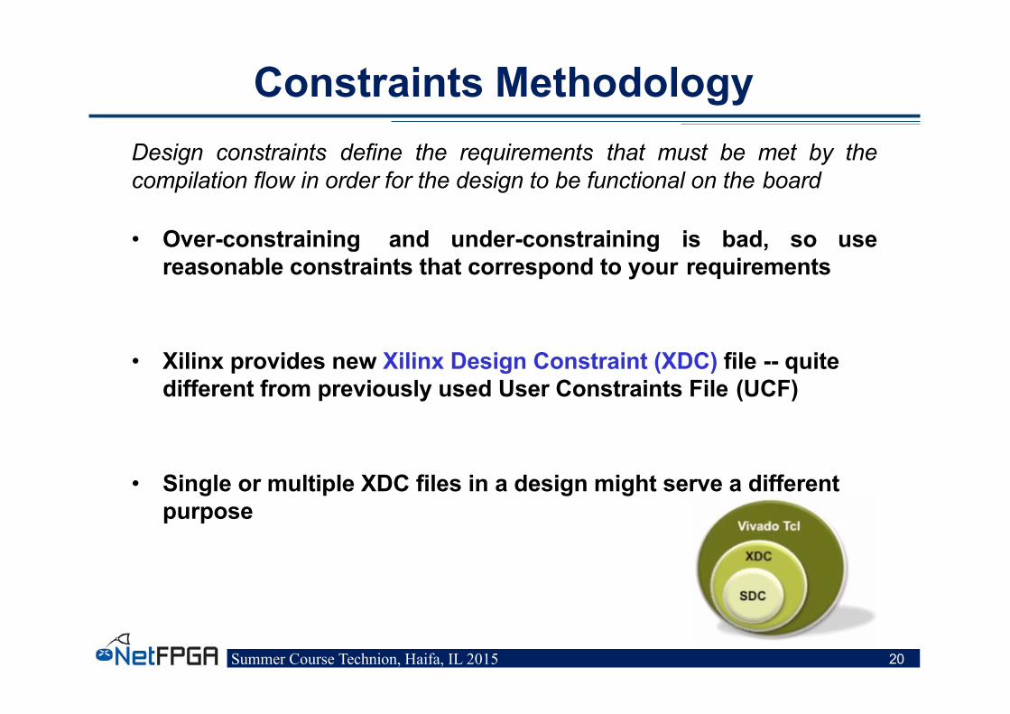
Constraints MethodologyDesign constraints define the requirements that must be met by the compilation flow in order for the design to be functional on the board
• Over-constraining and under-constraining is bad, so use reasonable constraints that correspond to your requirements
• Xilinx provides new Xilinx Design Constraint (XDC) file -- quite different from previously used User Constraints File (UCF)
• Single or multiple XDC files in a design might serve a different purpose
Summer Course Technion, Haifa, IL 2015 20

Xilinx Design Constraint fileXDC constraints are a combination of:• Synopsys Design Constraints format (SDC)• Xilinx centric extensions• Tcl-compatible for advanced scripting
XDC constraints have the following properties:• follow the Tcl semantic,• interpreted like any other Tcl command,• read in and parsed sequentially.
You can use constraints for:• Synthesis and/or Implementation
Options are specified in file properties or via tcl :set_property used_in_synthesis false [get_files wave_gen_pins.xdc]set_property used_in_implementation true [get_files wave_gen_pins.xdc]
Summer Course Technion, Haifa, IL 2015 21

XDC File Order
Summer Course Technion, Haifa, IL 2015 22
The constraint files are loaded in the same sequence as the way they are listed
To change order either drag and drop or reorder using: reorder_files -fileset constrs_1 -before [get_files wave_gen_timing.xdc] \[get_files wave_gen_pins.xdc]
IPs:If you use the native IPs, their XDC files are loaded after your files
You cannot change the IP XDC files order, but you can disable them and re-apply constraints in your XDC files

Common pitfalls
Summer Course Technion, Haifa, IL 2015 23
Missing constraints:- The corresponding paths are not optimized for timing- No violation will be reported but design may not work on HW
Incorrect constraints:- Runtime and optimization efforts will be spent on the wrong paths- Reported timing violations may not result in any issues on HW
Unreasonable hold requirements:- May result in long runtime and SETUP violations- P&R fixes HOLD violations as #1 priority, because:
• Designs with HOLD violations won’t work on HW• Designs with SETUP violations will work, but slower

Timing report
Ø Report SummaryContains info about design, device, tool version, data and time of report
Ø Path summarySummarizes timing information for the path: timing is met (Slack), source anddestination, clock used, setup and hold check (requirements), number of level oflogic, skew and uncertainty
Summer Course Technion, Haifa, IL 2015 24

Timing command summary
Ø Create and validate clocks:– check_timing: for missing clocks and IO constraints– report_clocks: check frequency and phase– report_clock_networks: possible clock root
Ø Validate clock groups:– report_clock_interaction
Ø Validate I/O delays– report_timing –from [input_port] –setup/-hold– report_timing –to [output_port] –setup/-hold
Ø Add exceptions if necessary– Validate using report_timing
Summer Course Technion, Haifa, IL 2015 25

Summer Course Technion, Haifa, IL 2015 26
Once the bitfile is created you need to:
• Check if your design meet the timing.
• Debug your HW code if regression tests are not passed.
Debugging the design
Summer Course Technion, Haifa, IL 2015 27
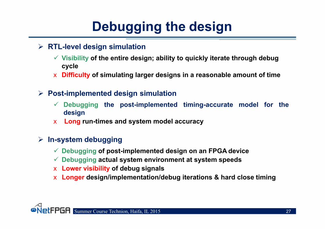
Ø RTL-level design simulationü Visibility of the entire design; ability to quickly iterate through debug
cyclex Difficulty of simulating larger designs in a reasonable amount of time
Ø Post-implemented design simulationmodel for theü Debugging the post-implemented timing-accurate
designx Long run-times and system model accuracy
Ø In-system debuggingü Debugging of post-implemented design on an FPGA deviceü Debugging actual system environment at system speedsx Lower visibility of debug signalsx Longer design/implementation/debug iterations & hard close timing

Integrated Logic Analyzer
Summer Course Technion, Haifa, IL 2015 28
Ø 1. Probing phase: Identifying what signals in your design you want to probe and how you want to probe them
Identifying what signals or nets you want to probe Deciding how you want to add debug cores to your design
Ø 2. Implementation phase: Implementing the design that includes the additional debug IP that is attached to the probed nets
The debug core hub must be implemented prior to running the PL & RT.
Ø 3. Analysis phase: Interacting with the debug IP contained in the design to debug and verify functional issues
Connecting to the Hardware Target and Programming the FPGA Device Setting up the ILA Core to Take a MeasurementViewing ILA Cores in the Debug Probes Window Using Basic Trigger ModeViewing ILA Probe Data in the Waveform Viewer

Inserting ILA cores
Summer Course Technion, Haifa, IL 2015 29
• Either Manually add the debug IP component instances through the source code, or
• Allow Vivado tool to automatically insert the debug cores into your post-synthesis netlist
The first approach is more straight forward:
Ø Start with Identifying signals for debugging at the HDL source level prior to synthesis
(* mark_debug = "true" *) wire [7:0] char_fifo_dout; -- Verilog example
Ø Once design is synthesized use Set up Debug wizard for core assignment and configuration

Inserting ILA cores (cont.)
You can insert it from GUI as well:
• Synthesize your design first
• Open synthesized design
• Set up debug
• The core can be seen in the Netlist folder
Summer Course Technion, Haifa, IL 2015 30
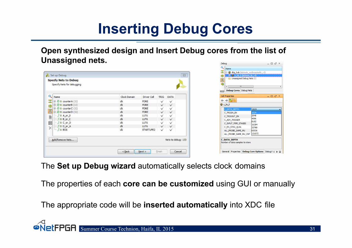
Inserting Debug CoresOpen synthesized design and Insert Debug cores from the list of Unassigned nets.
The Set up Debug wizard automatically selects clock domains
The properties of each core can be customized using GUI or manually
The appropriate code will be inserted automatically into XDC file
Summer Course Technion, Haifa, IL 2015 31

Inserting Debug Cores (cont.)
Summer Course Technion, Haifa, IL 2015 32
Ø XDC Commands can be also used to Insert Debug Corescreate_debug_core u_ila_0 ilaset_property C_DATA_DEPTH 1024 [get_debug_cores u_ila_0] set_property C_TRIGIN_EN false [get_debug_cores u_ila_0] set_property C_TRIGOUT_EN false [get_debug_cores u_ila_0] set_property C_ADV_TRIGGER false [get_debug_cores u_ila_0]…
Ø Saving constraints may cause the synthesis and implementation to go out-of-date;
Ø you do not need to re-synthesize the design since the debug XDC constraints are only used during implementation
Ø Check Xil UG908 for advanced debugging capabilities and IBERT

Debugging Logic Designs in Hardware1. Connect to the hardware target and program the FPGA with the .bit file2. Set up the ILA debug core trigger and capture controls.3. Arm the ILA debug core trigger.4. View the captured data from the ILA debug core in the Waveform window
Summer Course Technion, Haifa, IL 2015 33
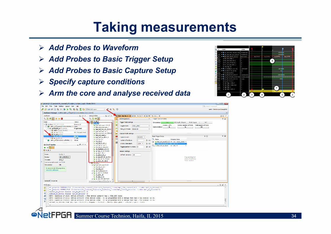
Taking measurementsØ Add Probes to WaveformØ Add Probes to Basic Trigger SetupØ Add Probes to Basic Capture SetupØ Specify capture conditionsØ Arm the core and analyse received data
Summer Course Technion, Haifa, IL 2015 34
Acknowledgments (I)
Summer Course Technion, Haifa, IL 2015 35
NetFPGA Team at University of Cambridge (Past and Present):Andrew Moore, David Miller, Muhammad Shahbaz, Martin Zadnik
Matthew Grosvenor, Yury Audzevich, Neelakandan Manihatty-Bojan, Georgina Kalogeridou, Jong Hun Han, Noa Zilberman, Gianni Antichi, Charalampos Rotsos, Marco Forconesi, Jinyun Zhang, Bjoern Zeeb
NetFPGA Team at Stanford University (Past and Present):Nick McKeown, Glen Gibb, Jad Naous, David Erickson,
G. Adam Covington, John W. Lockwood, Jianying Luo, Brandon Heller, Paul Hartke, Neda Beheshti, Sara Bolouki, James Zeng,
Jonathan Ellithorpe, Sachidanandan Sambandan, Eric LoAll Community members (including but not limited to):
Paul Rodman, Kumar Sanghvi, Wojciech A. Koszek, Yahsar Ganjali, Martin Labrecque, Jeff Shafer, Eric Keller , Tatsuya Yabe, Bilal Anwer, Yashar Ganjali, Martin Labrecque,
Lisa Donatini, Sergio Lopez-Buedo
Kees Vissers, Michaela Blott, Shep Siegel, Cathal McCabe

Acknowledgements (II)
Disclaimer: Any opinions, findings, conclusions, or recommendations expressed in these materials do not necessarily reflect the views of the National Science Foundation or of any other sponsors supporting this project.This effort is also sponsored by the Defense Advanced Research Projects Agency (DARPA) and the Air Force Research Laboratory (AFRL), under contract FA8750-11-C-0249. This material is approved for public release, distribution unlimited. The views expressed are those of the authors and do not reflect the official policy or position of the Department of Defense or the U.S. Government.
Summer Course Technion, Haifa, IL 2015 36