2016.10.24 eksprimenter - pdf v.01 - Innlagt av Sven Åge Eriksen Fagskolen Telemark ...
423
First Edition, last update January 18, 2010
-
Upload
sven-age-eriksen -
Category
Education
-
view
30 -
download
3
Transcript of 2016.10.24 eksprimenter - pdf v.01 - Innlagt av Sven Åge Eriksen Fagskolen Telemark ...

First Edition, last update January 18, 2010

2

Lessons In Electric Circuits, Volume VI – Experiments
By Tony R. Kuphaldt
First Edition, last update January 18, 2010

i
c©2002-2015, Tony R. Kuphaldt
This book is published under the terms and conditions of the Design Science License. Theseterms and conditions allow for free copying, distribution, and/or modification of this documentby the general public. The full Design Science License text is included in the last chapter.
As an open and collaboratively developed text, this book is distributed in the hope thatit will be useful, but WITHOUT ANY WARRANTY; without even the implied warranty ofMERCHANTABILITY or FITNESS FOR A PARTICULAR PURPOSE. See the Design ScienceLicense for more details.
Available in its entirety as part of the Open Book Project collection at:
openbookproject.net/electricCircuits
PRINTING HISTORY
• First Edition: Printed in April 2002. Source files written in SubML format. SubML is asimple markup language designed to easily convert to other markups like LATEX, HTML,or DocBook using nothing but search-and-replace substitutions.

ii

Contents
1 INTRODUCTION 1
1.1 Electronics as science . . . . . . . . . . . . . . . . . . . . . . . . . . . . . . . . . . 11.2 Setting up a home lab . . . . . . . . . . . . . . . . . . . . . . . . . . . . . . . . . . 31.3 Contributors . . . . . . . . . . . . . . . . . . . . . . . . . . . . . . . . . . . . . . . . 14
2 BASIC CONCEPTS AND TEST EQUIPMENT 15
2.1 Voltmeter usage . . . . . . . . . . . . . . . . . . . . . . . . . . . . . . . . . . . . . . 152.2 Ohmmeter usage . . . . . . . . . . . . . . . . . . . . . . . . . . . . . . . . . . . . . 212.3 A very simple circuit . . . . . . . . . . . . . . . . . . . . . . . . . . . . . . . . . . . 282.4 Ammeter usage . . . . . . . . . . . . . . . . . . . . . . . . . . . . . . . . . . . . . . 352.5 Ohm’s Law . . . . . . . . . . . . . . . . . . . . . . . . . . . . . . . . . . . . . . . . . 422.6 Nonlinear resistance . . . . . . . . . . . . . . . . . . . . . . . . . . . . . . . . . . . 452.7 Power dissipation . . . . . . . . . . . . . . . . . . . . . . . . . . . . . . . . . . . . . 482.8 Circuit with a switch . . . . . . . . . . . . . . . . . . . . . . . . . . . . . . . . . . . 532.9 Electromagnetism . . . . . . . . . . . . . . . . . . . . . . . . . . . . . . . . . . . . 552.10 Electromagnetic induction . . . . . . . . . . . . . . . . . . . . . . . . . . . . . . . . 57
3 DC CIRCUITS 59
3.1 Introduction . . . . . . . . . . . . . . . . . . . . . . . . . . . . . . . . . . . . . . . . 593.2 Series batteries . . . . . . . . . . . . . . . . . . . . . . . . . . . . . . . . . . . . . . 603.3 Parallel batteries . . . . . . . . . . . . . . . . . . . . . . . . . . . . . . . . . . . . . 633.4 Voltage divider . . . . . . . . . . . . . . . . . . . . . . . . . . . . . . . . . . . . . . 673.5 Current divider . . . . . . . . . . . . . . . . . . . . . . . . . . . . . . . . . . . . . . 783.6 Potentiometer as a voltage divider . . . . . . . . . . . . . . . . . . . . . . . . . . . 873.7 Potentiometer as a rheostat . . . . . . . . . . . . . . . . . . . . . . . . . . . . . . . 933.8 Precision potentiometer . . . . . . . . . . . . . . . . . . . . . . . . . . . . . . . . . 993.9 Rheostat range limiting . . . . . . . . . . . . . . . . . . . . . . . . . . . . . . . . . 1023.10 Thermoelectricity . . . . . . . . . . . . . . . . . . . . . . . . . . . . . . . . . . . . . 1093.11 Make your own multimeter . . . . . . . . . . . . . . . . . . . . . . . . . . . . . . . 1123.12 Sensitive voltage detector . . . . . . . . . . . . . . . . . . . . . . . . . . . . . . . . 1173.13 Potentiometric voltmeter . . . . . . . . . . . . . . . . . . . . . . . . . . . . . . . . 1223.14 4-wire resistance measurement . . . . . . . . . . . . . . . . . . . . . . . . . . . . . 1273.15 A very simple computer . . . . . . . . . . . . . . . . . . . . . . . . . . . . . . . . . 1313.16 Potato battery . . . . . . . . . . . . . . . . . . . . . . . . . . . . . . . . . . . . . . . 136
iii

iv CONTENTS
3.17 Capacitor charging and discharging . . . . . . . . . . . . . . . . . . . . . . . . . . 138
3.18 Rate-of-change indicator . . . . . . . . . . . . . . . . . . . . . . . . . . . . . . . . . 142
4 AC CIRCUITS 145
4.1 Introduction . . . . . . . . . . . . . . . . . . . . . . . . . . . . . . . . . . . . . . . . 145
4.2 Transformer – power supply . . . . . . . . . . . . . . . . . . . . . . . . . . . . . . 147
4.3 Build a transformer . . . . . . . . . . . . . . . . . . . . . . . . . . . . . . . . . . . 151
4.4 Variable inductor . . . . . . . . . . . . . . . . . . . . . . . . . . . . . . . . . . . . . 153
4.5 Sensitive audio detector . . . . . . . . . . . . . . . . . . . . . . . . . . . . . . . . . 155
4.6 Sensing AC magnetic fields . . . . . . . . . . . . . . . . . . . . . . . . . . . . . . . 160
4.7 Sensing AC electric fields . . . . . . . . . . . . . . . . . . . . . . . . . . . . . . . . 162
4.8 Automotive alternator . . . . . . . . . . . . . . . . . . . . . . . . . . . . . . . . . . 164
4.9 Induction motor . . . . . . . . . . . . . . . . . . . . . . . . . . . . . . . . . . . . . . 170
4.10 Induction motor, large . . . . . . . . . . . . . . . . . . . . . . . . . . . . . . . . . . 174
4.11 Phase shift . . . . . . . . . . . . . . . . . . . . . . . . . . . . . . . . . . . . . . . . . 177
4.12 Sound cancellation . . . . . . . . . . . . . . . . . . . . . . . . . . . . . . . . . . . . 180
4.13 Musical keyboard as a signal generator . . . . . . . . . . . . . . . . . . . . . . . . 183
4.14 PC Oscilloscope . . . . . . . . . . . . . . . . . . . . . . . . . . . . . . . . . . . . . . 186
4.15 Waveform analysis . . . . . . . . . . . . . . . . . . . . . . . . . . . . . . . . . . . . 189
4.16 Inductor-capacitor ”tank” circuit . . . . . . . . . . . . . . . . . . . . . . . . . . . . 191
4.17 Signal coupling . . . . . . . . . . . . . . . . . . . . . . . . . . . . . . . . . . . . . . 194
5 DISCRETE SEMICONDUCTOR CIRCUITS 201
5.1 Introduction . . . . . . . . . . . . . . . . . . . . . . . . . . . . . . . . . . . . . . . . 202
5.2 Commutating diode . . . . . . . . . . . . . . . . . . . . . . . . . . . . . . . . . . . 203
5.3 Half-wave rectifier . . . . . . . . . . . . . . . . . . . . . . . . . . . . . . . . . . . . 205
5.4 Full-wave center-tap rectifier . . . . . . . . . . . . . . . . . . . . . . . . . . . . . . 213
5.5 Full-wave bridge rectifier . . . . . . . . . . . . . . . . . . . . . . . . . . . . . . . . 218
5.6 Rectifier/filter circuit . . . . . . . . . . . . . . . . . . . . . . . . . . . . . . . . . . . 221
5.7 Voltage regulator . . . . . . . . . . . . . . . . . . . . . . . . . . . . . . . . . . . . . 227
5.8 Transistor as a switch . . . . . . . . . . . . . . . . . . . . . . . . . . . . . . . . . . 230
5.9 Static electricity sensor . . . . . . . . . . . . . . . . . . . . . . . . . . . . . . . . . 235
5.10 Pulsed-light sensor . . . . . . . . . . . . . . . . . . . . . . . . . . . . . . . . . . . . 238
5.11 Voltage follower . . . . . . . . . . . . . . . . . . . . . . . . . . . . . . . . . . . . . . 241
5.12 Common-emitter amplifier . . . . . . . . . . . . . . . . . . . . . . . . . . . . . . . 246
5.13 Multi-stage amplifier . . . . . . . . . . . . . . . . . . . . . . . . . . . . . . . . . . . 251
5.14 Current mirror . . . . . . . . . . . . . . . . . . . . . . . . . . . . . . . . . . . . . . 255
5.15 JFET current regulator . . . . . . . . . . . . . . . . . . . . . . . . . . . . . . . . . 261
5.16 Differential amplifier . . . . . . . . . . . . . . . . . . . . . . . . . . . . . . . . . . . 266
5.17 Simple op-amp . . . . . . . . . . . . . . . . . . . . . . . . . . . . . . . . . . . . . . 269
5.18 Audio oscillator . . . . . . . . . . . . . . . . . . . . . . . . . . . . . . . . . . . . . . 274
5.19 Vacuum tube audio amplifier . . . . . . . . . . . . . . . . . . . . . . . . . . . . . . 277
Bibliography . . . . . . . . . . . . . . . . . . . . . . . . . . . . . . . . . . . . . . . . . . . 288

CONTENTS v
6 ANALOG INTEGRATED CIRCUITS 289
6.1 Introduction . . . . . . . . . . . . . . . . . . . . . . . . . . . . . . . . . . . . . . . . 2896.2 Voltage comparator . . . . . . . . . . . . . . . . . . . . . . . . . . . . . . . . . . . . 2916.3 Precision voltage follower . . . . . . . . . . . . . . . . . . . . . . . . . . . . . . . . 2946.4 Noninverting amplifier . . . . . . . . . . . . . . . . . . . . . . . . . . . . . . . . . . 2986.5 High-impedance voltmeter . . . . . . . . . . . . . . . . . . . . . . . . . . . . . . . 3016.6 Integrator . . . . . . . . . . . . . . . . . . . . . . . . . . . . . . . . . . . . . . . . . 3056.7 555 audio oscillator . . . . . . . . . . . . . . . . . . . . . . . . . . . . . . . . . . . . 3116.8 555 ramp generator . . . . . . . . . . . . . . . . . . . . . . . . . . . . . . . . . . . 3146.9 PWM power controller . . . . . . . . . . . . . . . . . . . . . . . . . . . . . . . . . . 3176.10 Class B audio amplifier . . . . . . . . . . . . . . . . . . . . . . . . . . . . . . . . . 321
7 DIGITAL INTEGRATED CIRCUITS 331
7.1 Introduction . . . . . . . . . . . . . . . . . . . . . . . . . . . . . . . . . . . . . . . . 3317.2 Basic gate function . . . . . . . . . . . . . . . . . . . . . . . . . . . . . . . . . . . . 3337.3 NOR gate S-R latch . . . . . . . . . . . . . . . . . . . . . . . . . . . . . . . . . . . . 3377.4 NAND gate S-R enabled latch . . . . . . . . . . . . . . . . . . . . . . . . . . . . . 3417.5 NAND gate S-R flip-flop . . . . . . . . . . . . . . . . . . . . . . . . . . . . . . . . . 3437.6 LED sequencer . . . . . . . . . . . . . . . . . . . . . . . . . . . . . . . . . . . . . . 3477.7 Simple combination lock . . . . . . . . . . . . . . . . . . . . . . . . . . . . . . . . . 3567.8 3-bit binary counter . . . . . . . . . . . . . . . . . . . . . . . . . . . . . . . . . . . 3597.9 7-segment display . . . . . . . . . . . . . . . . . . . . . . . . . . . . . . . . . . . . 361
8 555 TIMER CIRCUITS 365
8.1 The 555 IC . . . . . . . . . . . . . . . . . . . . . . . . . . . . . . . . . . . . . . . . . 3658.2 555 Schmitt Trigger . . . . . . . . . . . . . . . . . . . . . . . . . . . . . . . . . . . 3668.3 555 HYSTERETIC OSCILLATOR . . . . . . . . . . . . . . . . . . . . . . . . . . . 3708.4 555 MONOSTABLE MULTIVIBRATOR . . . . . . . . . . . . . . . . . . . . . . . 3748.5 CMOS 555 LONG DURATION MINIMUM PARTS RED LED FLASHER . . . . 3808.6 CMOS 555 LONG DURATION BLUE LED FLASHER . . . . . . . . . . . . . . . 3858.7 CMOS 555 LONG DURATION FLYBACK LED FLASHER . . . . . . . . . . . . 3898.8 HOW TO MAKE AN INDUCTOR . . . . . . . . . . . . . . . . . . . . . . . . . . . 3928.9 CMOS 555 LONG DURATION RED LED FLASHER . . . . . . . . . . . . . . . . 395
A-1 ABOUT THIS BOOK 399
A-2 CONTRIBUTOR LIST 403
A-3 DESIGN SCIENCE LICENSE 407
INDEX 410

Chapter 1
INTRODUCTION
Contents
1.1 Electronics as science . . . . . . . . . . . . . . . . . . . . . . . . . . . . . . . . 1
1.2 Setting up a home lab . . . . . . . . . . . . . . . . . . . . . . . . . . . . . . . . 3
1.2.1 Work area . . . . . . . . . . . . . . . . . . . . . . . . . . . . . . . . . . . . 3
1.2.2 Tools . . . . . . . . . . . . . . . . . . . . . . . . . . . . . . . . . . . . . . . 3
1.2.3 Supplies . . . . . . . . . . . . . . . . . . . . . . . . . . . . . . . . . . . . . 12
1.3 Contributors . . . . . . . . . . . . . . . . . . . . . . . . . . . . . . . . . . . . . . 14
1.1 Electronics as science
Electronics is a science, and a very accessible science at that. With other areas of scientificstudy, expensive equipment is generally required to perform any non-trivial experiments. Notso with electronics. Many advanced concepts may be explored using parts and equipmenttotaling under a few hundred US dollars. This is good, because hands-on experimentation isvital to gaining scientific knowledge about any subject.
When I started writing Lessons In Electric Circuits, my intent was to create a textbooksuitable for introductory college use. However, being mostly self-taught in electronics myself,I knew the value of a good textbook to hobbyists and experimenters not enrolled in any formalelectronics course. Many people selflessly volunteered their time and expertise in helping melearn electronics when I was younger, and my intent is to honor their service and love by givingback to the world what they gave to me.
In order for someone to teach themselves a science such as electronics, they must engage inhands-on experimentation. Knowledge gleaned from books alone has limited use, especially inscientific endeavors. If my contribution to society is to be complete, I must include a guide toexperimentation along with the text(s) on theory, so that the individual learning on their ownhas a resource to guide their experimental adventures.
A formal laboratory course for college electronics study requires an enormous amount ofwork to prepare, and usually must be based around specific parts and equipment so that the
1

2 CHAPTER 1. INTRODUCTION
experiments will be sufficient detailed, with results sufficiently precise to allow for rigorouscomparison between experimental and theoretical data. A process of assessment, articulatedthrough a qualified instructor, is also vital to guarantee that a certain level of learning hastaken place. Peer review (comparison of experimental results with the work of others) is an-other important component of college-level laboratory study, and helps to improve the qualityof learning. Since I cannot meet these criteria through the medium of a book, it is impracticalfor me to present a complete laboratory course here. In the interest of keeping this experimentguide reasonably low-cost for people to follow, and practical for deployment over the internet, Iam forced to design the experiments at a lower level than what would be expected for a collegelab course.
The experiments in this volume begin at a level appropriate for someone with no electronicsknowledge, and progress to higher levels. They stress qualitative knowledge over quantitativeknowledge, although they could serve as templates for more rigorous coursework. If thereis any portion of Lessons In Electric Circuits that will remain ”incomplete,” it is this one: Ifully intend to continue adding experiments ad infinitum so as to provide the experimenter orhobbyist with a wealth of ideas to explore the science of electronics. This volume of the bookseries is also the easiest to contribute to, for those who would like to help me in providing freeinformation to people learning electronics. It doesn’t take a tremendous effort to describe anexperiment or two, and I will gladly include it if you email it to me, giving you full credit forthe work. Refer to Appendix 2 for details on contributing to this book.
When performing these experiments, feel free to explore by trying different circuit construc-tion and measurement techniques. If something isn’t working as the text describes it should,don’t give up! It’s probably due to a simple problem in construction (loose wire, wrong com-ponent value) or test equipment setup. It can be frustrating working through these problemson your own, but the knowledge gained by ”troubleshooting” a circuit yourself is at least asimportant as the knowledge gained by a properly functioning experiment. This is one of themost important reasons why experimentation is so vital to your scientific education: the realproblems you will invariably encounter in experimentation challenge you to develop practicalproblem-solving skills.
In many of these experiments, I offer part numbers for Radio Shack brand components. Thisis not an endorsement of Radio Shack, but simply a convenient reference to an electronic supplycompany well-known in North America. Often times, components of better quality and lowerprice may be obtained through mail-order companies and other, lesser-known supply houses. Istrongly recommend that experimenters obtain some of the more expensive components suchas transformers (see the AC chapter) by salvaging them from discarded electrical appliances,both for economic and ecological reasons.
All experiments shown in this book are designed with safety in mind. It is nearly impossibleto shock or otherwise hurt yourself by battery-powered experiments or other circuits of lowvoltage. However, hazards do exist building anything with your own two hands. Where thereis a greater-than-normal level of danger in an experiment, I take efforts to direct the reader’sattention toward it. However, it is unfortunately necessary in this litigious society to disclaimany and all liability for the outcome of any experiment presented here. Neither myself norany contributors bear responsibility for injuries resulting from the construction or use of anyof these projects, from the mis-handling of electricity by the experimenter, or from any otherunsafe practices leading to injury. Perform these experiments at your own risk!

1.2. SETTING UP A HOME LAB 3
1.2 Setting up a home lab
In order to build the circuits described in this volume, you will need a small work area, aswell as a few tools and critical supplies. This section describes the setup of a home electronicslaboratory.
1.2.1 Work area
A work area should consist of a large workbench, desk, or table (preferably wooden) for per-forming circuit assembly, with household electrical power (120 volts AC) readily accessible topower soldering equipment, power supplies, and any test equipment. Inexpensive desks in-tended for computer use function very well for this purpose. Avoid a metal-surface desk, as theelectrical conductivity of a metal surface creates both a shock hazard and the very distinct pos-sibility of unintentional ”short circuits” developing from circuit components touching the metaltabletop. Vinyl and plastic bench surfaces are to be avoided for their ability to generate andstore large static-electric charges, which may damage sensitive electronic components. Also,these materials melt easily when exposed to hot soldering irons and molten solder droplets.
If you cannot obtain a wooden-surface workbench, you may turn any form of table or deskinto one by laying a piece of plywood on top. If you are reasonably skilled with woodworkingtools, you may construct your own desk using plywood and 2x4 boards.
The work area should be well-lit and comfortable. I have a small radio set up on my ownworkbench for listening to music or news as I experiment. My own workbench has a ”powerstrip” receptacle and switch assembly mounted to the underside, into which I plug all 120volt devices. It is convenient to have a single switch for shutting off all power in case of anaccidental short-circuit!
1.2.2 Tools
A few tools are required for basic electronics work. Most of these tools are inexpensive and easyto obtain. If you desire to keep the cost as low as possible, you might want to search for themat thrift stores and pawn shops before buying them new. As you can tell from the photographs,some of my own tools are rather old but function well nonetheless.
First and foremost in your tool collection is a multimeter. This is an electrical instrumentdesigned to measure voltage, current, resistance, and often other variables as well. Multime-ters are manufactured in both digital and analog form. A digital multimeter is preferred forprecision work, but analog meters are also useful for gaining an intuitive understanding ofinstrument sensitivity and range.
My own digital multimeter is a Fluke model 27, purchased in 1987:
Digital multimeter

4 CHAPTER 1. INTRODUCTION
Most analog multimeters sold today are quite inexpensive, and not necessarily precisiontest instruments. I recommend having both digital and analog meter types in your tool collec-tion, spending as little money as possible on the analog multimeter and investing in a good-quality digital multimeter (I highly recommend the Fluke brand).
======================================
A test instrument I have found indispensable in my home work is a sensitive voltage de-
tector, or sensitive audio detector, described in nearly identical experiments in two chaptersof this book volume. It is nothing more than a sensitized set of audio headphones, equippedwith an attenuator (volume control) and limiting diodes to limit sound intensity from strongsignals. Its purpose is to audibly indicate the presence of low-intensity voltage signals, DC orAC. In the absence of an oscilloscope, this is a most valuable tool, because it allows you to lis-
ten to an electronic signal, and thereby determine something of its nature. Few tools engenderan intuitive comprehension of frequency and amplitude as this! I cite its use in many of theexperiments shown in this volume, so I strongly encourage that you build your own. Secondonly to a multimeter, it is the most useful piece of test equipment in the collection of the budgetelectronics experimenter.
Sensitive voltage/audio detector

1.2. SETTING UP A HOME LAB 5
As you can see, I built my detector using scrap parts (household electrical switch/receptaclebox for the enclosure, section of brown lamp cord for the test leads). Even some of the internalcomponents were salvaged from scrap (the step-down transformer and headphone jack weretaken from an old radio, purchased in non-working condition from a thrift store). The en-tire thing, including the headphones purchased second-hand, cost no more than $15 to build.Of course, one could take much greater care in choosing construction materials (metal box,shielded test probe cable), but it probably wouldn’t improve its performance significantly.
The single most influential component with regard to detector sensitivity is the headphoneassembly: generally speaking, the greater the ”dB” rating of the headphones, the better theywill function for this purpose. Since the headphones need not be modified for use in the detectorcircuit, and they can be unplugged from it, you might justify the purchase of more expensive,high-quality headphones by using them as part of a home entertainment (audio/video) system.
======================================
Also essential is a solderless breadboard, sometimes called a prototyping board, or proto-
board. This device allows you to quickly join electronic components to one another withouthaving to solder component terminals and wires together.
Solderless breadboard
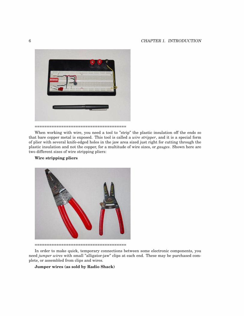
6 CHAPTER 1. INTRODUCTION
======================================
When working with wire, you need a tool to ”strip” the plastic insulation off the ends sothat bare copper metal is exposed. This tool is called a wire stripper, and it is a special formof plier with several knife-edged holes in the jaw area sized just right for cutting through theplastic insulation and not the copper, for a multitude of wire sizes, or gauges. Shown here aretwo different sizes of wire stripping pliers:
Wire stripping pliers
======================================
In order to make quick, temporary connections between some electronic components, youneed jumper wires with small ”alligator-jaw” clips at each end. These may be purchased com-plete, or assembled from clips and wires.
Jumper wires (as sold by Radio Shack)

1.2. SETTING UP A HOME LAB 7
Jumper wires (home-made)
The home-made jumper wires with large, uninsulated (bare metal) alligator clips are okayto use so long as care is taken to avoid any unintentional contact between the bare clips andany other wires or components. For use in crowded breadboard circuits, jumper wires withinsulated (rubber-covered) clips like the jumper shown from Radio Shack are much preferred.
======================================
Needle-nose pliers are designed to grasp small objects, and are especially useful for pushingwires into stubborn breadboard holes.
Needle-nose pliers

8 CHAPTER 1. INTRODUCTION
======================================No tool set would be complete without screwdrivers, and I recommend a complementary
pair (3/16 inch slotted and #2 Phillips) as the starting point for your collection. You may laterfind it useful to invest in a set of jeweler’s screwdrivers for work with very small screws andscrew-head adjustments.
Screwdrivers
======================================For projects involving printed-circuit board assembly or repair, a small soldering iron and a
spool of ”rosin-core” solder are essential tools. I recommend a 25 watt soldering iron, no largerfor printed circuit board work, and the thinnest solder you can find. Do not use ”acid-core”
solder! Acid-core solder is intended for the soldering of copper tubes (plumbing), where a smallamount of acid helps to clean the copper of surface impurities and provide a stronger bond. Ifused for electrical work, the residual acid will cause wires to corrode. Also, you should avoidsolder containing the metal lead, opting instead for silver-alloy solder. If you do not alreadywear glasses, a pair of safety glasses is highly recommended while soldering, to prevent bits of

1.2. SETTING UP A HOME LAB 9
molten solder from accidently landing in your eye should a wire release from the joint duringthe soldering process and fling bits of solder toward you.
Soldering iron and solder (”rosin core”)
======================================
Projects requiring the joining of large wires by soldering will necessitate a more powerfulheat source than a 25 watt soldering iron. A soldering gun is a practical option.
Soldering gun
======================================
Knives, like screwdrivers, are essential tools for all kinds of work. For safety’s sake, Irecommend a ”utility” knife with retracting blade. These knives are also advantageous to havefor their ability to accept replacement blades.
Utility knife

10 CHAPTER 1. INTRODUCTION
======================================
Pliers other than the needle-nose type are useful for the assembly and disassembly of elec-tronic device chassis. Two types I recommend are slip-joint and adjustable-joint (”Channel-lock”).
Slip-joint pliers
Adjustable-joint pliers

1.2. SETTING UP A HOME LAB 11
======================================Drilling may be required for the assembly of large projects. Although power drills work
well, I have found that a simple hand-crank drill does a remarkable job drilling through plastic,wood, and most metals. It is certainly safer and quieter than a power drill, and costs quite abit less.
Hand drill
As the wear on my drill indicates, it is an often-used tool around my home!======================================Some experiments will require a source of audio-frequency voltage signals. Normally, this
type of signal is generated in an electronics laboratory by a device called a signal generator
or function generator. While building such a device is not impossible (nor difficult!), it oftenrequires the use of an oscilloscope to fine-tune, and oscilloscopes are usually outside the bud-getary range of the home experimenter. A relatively inexpensive alternative to a commercialsignal generator is an electronic keyboard of the musical type. You need not be a musician tooperate one for the purposes of generating an audio signal (just press any key on the board!),

12 CHAPTER 1. INTRODUCTION
and they may be obtained quite readily at second-hand stores for substantially less than newprice. The electronic signal generated by the keyboard is conducted to your circuit via a head-phone cable plugged into the ”headphones” jack. More details regarding the use of a ”MusicalKeyboard as a Signal Generator” may be found in the experiment of that name in chapter 4(AC).
1.2.3 Supplies
Wire used in solderless breadboards must be 22-gauge, solid copper. Spools of this wire areavailable from electronic supply stores and some hardware stores, in different insulation colors.Insulation color has no bearing on the wire’s performance, but different colors are sometimesuseful for ”color-coding” wire functions in a complex circuit.
Spool of 22-gauge, solid copper wire
Note how the last 1/4 inch or so of the copper wire protruding from the spool has been”stripped” of its plastic insulation.
======================================
An alternative to solderless breadboard circuit construction is wire-wrap, where 30-gauge(very thin!) solid copper wire is tightly wrapped around the terminals of components insertedthrough the holes of a fiberglass board. No soldering is required, and the connections made areat least as durable as soldered connections, perhaps more. Wire-wrapping requires a spool ofthis very thin wire, and a special wrapping tool, the simplest kind resembling a small screw-driver.
Wire-wrap wire and wrapping tool
1.2. SETTING UP A HOME LAB 13
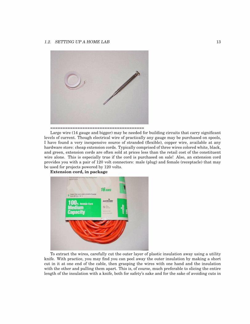
======================================Large wire (14 gauge and bigger) may be needed for building circuits that carry significant
levels of current. Though electrical wire of practically any gauge may be purchased on spools,I have found a very inexpensive source of stranded (flexible), copper wire, available at anyhardware store: cheap extension cords. Typically comprised of three wires colored white, black,and green, extension cords are often sold at prices less than the retail cost of the constituentwire alone. This is especially true if the cord is purchased on sale! Also, an extension cordprovides you with a pair of 120 volt connectors: male (plug) and female (receptacle) that maybe used for projects powered by 120 volts.
Extension cord, in package
To extract the wires, carefully cut the outer layer of plastic insulation away using a utilityknife. With practice, you may find you can peel away the outer insulation by making a shortcut in it at one end of the cable, then grasping the wires with one hand and the insulationwith the other and pulling them apart. This is, of course, much preferable to slicing the entirelength of the insulation with a knife, both for safety’s sake and for the sake of avoiding cuts in

14 CHAPTER 1. INTRODUCTION
the individual wires’ insulation.======================================During the course of building many circuits, you will accumulate a large number of small
components. One technique for keeping these components organized is to keep them in aplastic ”organizer” box like the type used for fishing tackle.
Component box
In this view of one of my component boxes, you can see plenty of 1/8 watt resistors, transis-tors, diodes, and even a few 8-pin integrated circuits (”chips”). Labels for each compartmentwere made with a permanent ink marker.
1.3 Contributors
Contributors to this chapter are listed in chronological order of their contributions, from mostrecent to first. See Appendix 2 (Contributor List) for dates and contact information.
Michael Warner (April 9, 2002): Suggestions for a section describing home laboratorysetup.

Chapter 2
BASIC CONCEPTS AND TEST
EQUIPMENT
Contents
2.1 Voltmeter usage . . . . . . . . . . . . . . . . . . . . . . . . . . . . . . . . . . . . 15
2.2 Ohmmeter usage . . . . . . . . . . . . . . . . . . . . . . . . . . . . . . . . . . . 21
2.3 A very simple circuit . . . . . . . . . . . . . . . . . . . . . . . . . . . . . . . . . 28
2.4 Ammeter usage . . . . . . . . . . . . . . . . . . . . . . . . . . . . . . . . . . . . 35
2.5 Ohm’s Law . . . . . . . . . . . . . . . . . . . . . . . . . . . . . . . . . . . . . . . 42
2.6 Nonlinear resistance . . . . . . . . . . . . . . . . . . . . . . . . . . . . . . . . . 45
2.7 Power dissipation . . . . . . . . . . . . . . . . . . . . . . . . . . . . . . . . . . . 48
2.8 Circuit with a switch . . . . . . . . . . . . . . . . . . . . . . . . . . . . . . . . 53
2.9 Electromagnetism . . . . . . . . . . . . . . . . . . . . . . . . . . . . . . . . . . 55
2.10 Electromagnetic induction . . . . . . . . . . . . . . . . . . . . . . . . . . . . . 57
2.1 Voltmeter usage
PARTS AND MATERIALS
• Multimeter, digital or analog
• Assorted batteries
• One light-emitting diode (Radio Shack catalog # 276-026 or equivalent)
• Small ”hobby” motor, permanent-magnet type (Radio Shack catalog # 273-223 or equiva-lent)
15

16 CHAPTER 2. BASIC CONCEPTS AND TEST EQUIPMENT
• Two jumper wires with ”alligator clip” ends (Radio Shack catalog # 278-1156, 278-1157,or equivalent)
A multimeter is an electrical instrument capable of measuring voltage, current, and re-sistance. Digital multimeters have numerical displays, like digital clocks, for indicating thequantity of voltage, current, or resistance. Analog multimeters indicate these quantities bymeans of a moving pointer over a printed scale.
Analog multimeters tend to be less expensive than digital multimeters, and more beneficialas learning tools for the first-time student of electricity. I strongly recommend purchasing ananalog multimeter before purchasing a digital multimeter, but to eventually have both in yourtool kit for these experiments.
CROSS-REFERENCES
Lessons In Electric Circuits, Volume 1, chapter 1: ”Basic Concepts of Electricity”
Lessons In Electric Circuits, Volume 1, chapter 8: ”DC Metering Circuits”
LEARNING OBJECTIVES
• How to measure voltage
• Characteristics of voltage: existing between two points
• Selection of proper meter range
ILLUSTRATION
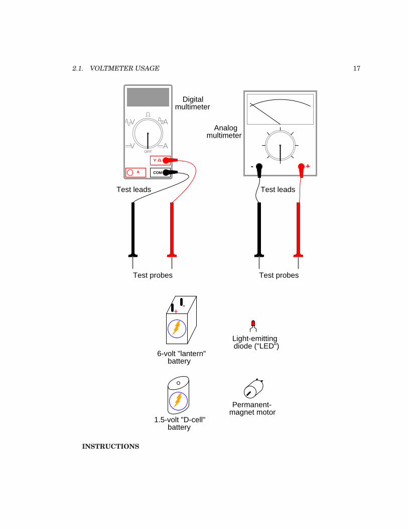
2.1. VOLTMETER USAGE 17
COMA
V
V A
AOFF
- +
Digitalmultimeter
Analogmultimeter
Test leads Test leads
Test probes Test probes
+-
6-volt "lantern"battery
Light-emittingdiode ("LED")
Permanent-magnet motor
1.5-volt "D-cell"battery
INSTRUCTIONS

18 CHAPTER 2. BASIC CONCEPTS AND TEST EQUIPMENT
In all the experiments in this book, you will be using some sort of test equipment to measureaspects of electricity you cannot directly see, feel, hear, taste, or smell. Electricity – at least insmall, safe quantities – is insensible by our human bodies. Your most fundamental ”eyes” in theworld of electricity and electronics will be a device called a multimeter. Multimeters indicatethe presence of, and measure the quantity of, electrical properties such as voltage, current, andresistance. In this experiment, you will familiarize yourself with the measurement of voltage.
Voltage is the measure of electrical ”push” ready to motivate electrons to move through aconductor. In scientific terms, it is the specific energy per unit charge, mathematically definedas joules per coulomb. It is analogous to pressure in a fluid system: the force that moves fluidthrough a pipe, and is measured in the unit of the Volt (V).
Your multimeter should come with some basic instructions. Read them well! If your mul-timeter is digital, it will require a small battery to operate. If it is analog, it does not need abattery to measure voltage.
Some digital multimeters are autoranging. An autoranging meter has only a few selec-tor switch (dial) positions. Manual-ranging meters have several different selector positionsfor each basic quantity: several for voltage, several for current, and several for resistance.Autoranging is usually found on only the more expensive digital meters, and is to manualranging as an automatic transmission is to a manual transmission in a car. An autorangingmeter ”shifts gears” automatically to find the best measurement range to display the particularquantity being measured.
Set your multimeter’s selector switch to the highest-value ”DC volt” position available. Au-toranging multimeters may only have a single position for DC voltage, in which case you needto set the switch to that one position. Touch the red test probe to the positive (+) side of abattery, and the black test probe to the negative (-) side of the same battery. The meter shouldnow provide you with some sort of indication. Reverse the test probe connections to the batteryif the meter’s indication is negative (on an analog meter, a negative value is indicated by thepointer deflecting left instead of right).
If your meter is a manual-range type, and the selector switch has been set to a high-rangeposition, the indication will be small. Move the selector switch to the next lower DC voltagerange setting and reconnect to the battery. The indication should be stronger now, as indicatedby a greater deflection of the analog meter pointer (needle), or more active digits on the digitalmeter display. For the best results, move the selector switch to the lowest-range setting thatdoes not ”over-range” the meter. An over-ranged analog meter is said to be ”pegged,” as theneedle will be forced all the way to the right-hand side of the scale, past the full-range scalevalue. An over-ranged digital meter sometimes displays the letters ”OL”, or a series of dashedlines. This indication is manufacturer-specific.
What happens if you only touch one meter test probe to one end of a battery? How does themeter have to connect to the battery in order to provide an indication? What does this tell usabout voltmeter use and the nature of voltage? Is there such a thing as voltage ”at” a singlepoint?
Be sure to measure more than one size of battery, and learn how to select the best voltagerange on the multimeter to give you maximum indication without over-ranging.
Now switch your multimeter to the lowest DC voltage range available, and touch the meter’stest probes to the terminals (wire leads) of the light-emitting diode (LED). An LED is designedto produce light when powered by a small amount of electricity, but LEDs also happen togenerate DC voltage when exposed to light, somewhat like a solar cell. Point the LED toward

2.1. VOLTMETER USAGE 19
a bright source of light with your multimeter connected to it, and note the meter’s indication:
- +
Light source
LED
Batteries develop electrical voltage through chemical reactions. When a battery ”dies,” ithas exhausted its original store of chemical ”fuel.” The LED, however, does not rely on aninternal ”fuel” to generate voltage; rather, it converts optical energy into electrical energy. Solong as there is light to illuminate the LED, it will produce voltage.
Another source of voltage through energy conversion a generator. The small electric mo-tor specified in the ”Parts and Materials” list functions as an electrical generator if its shaftis turned by a mechanical force. Connect your voltmeter (your multimeter, set to the ”volt”function) to the motor’s terminals just as you connected it to the LED’s terminals, and spinthe shaft with your fingers. The meter should indicate voltage by means of needle deflection(analog) or numerical readout (digital).
If you find it difficult to maintain both meter test probes in connection with the motor’sterminals while simultaneously spinning the shaft with your fingers, you may use alligator
clip ”jumper” wires like this:
- +Motor
Jumperwire
Alligatorclip

20 CHAPTER 2. BASIC CONCEPTS AND TEST EQUIPMENT
Determine the relationship between voltage and generator shaft speed? Reverse the gen-erator’s direction of rotation and note the change in meter indication. When you reverse shaftrotation, you change the polarity of the voltage created by the generator. The voltmeter indi-cates polarity by direction of needle direction (analog) or sign of numerical indication (digital).When the red test lead is positive (+) and the black test lead negative (-), the meter will registervoltage in the normal direction. If the applied voltage is of the reverse polarity (negative onred and positive on black), the meter will indicate ”backwards.”

2.2. OHMMETER USAGE 21
2.2 Ohmmeter usage
PARTS AND MATERIALS
• Multimeter, digital or analog
• Assorted resistors (Radio Shack catalog # 271-312 is a 500-piece assortment)
• Rectifying diode (1N4001 or equivalent; Radio Shack catalog # 276-1101)
• Cadmium Sulphide photocell (Radio Shack catalog # 276-1657)
• Breadboard (Radio Shack catalog # 276-174 or equivalent)
• Jumper wires
• Paper
• Pencil
• Glass of water
• Table salt
This experiment describes how to measure the electrical resistance of several objects. Youneed not possess all items listed above in order to effectively learn about resistance. Con-versely, you need not limit your experiments to these items. However, be sure to never mea-sure the resistance of any electrically ”live” object or circuit. In other words, do not attempt tomeasure the resistance of a battery or any other source of substantial voltage using a multi-meter set to the resistance (”ohms”) function. Failing to heed this warning will likely result inmeter damage and even personal injury.
CROSS-REFERENCES
Lessons In Electric Circuits, Volume 1, chapter 1: ”Basic Concepts of Electricity”Lessons In Electric Circuits, Volume 1, chapter 8: ”DC Metering Circuits”
LEARNING OBJECTIVES
• Determination and comprehension of ”electrical continuity”
• Determination and comprehension of ”electrically common points”
• How to measure resistance
• Characteristics of resistance: existing between two points
• Selection of proper meter range
• Relative conductivity of various components and materials
22 CHAPTER 2. BASIC CONCEPTS AND TEST EQUIPMENT
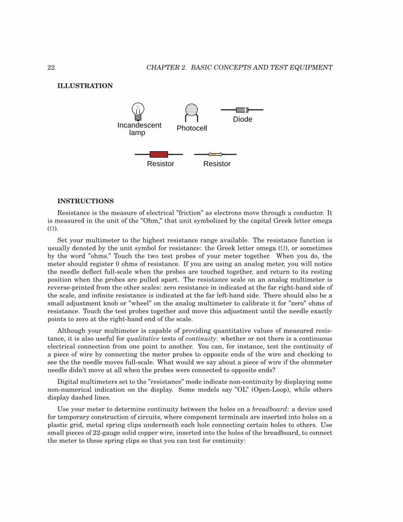
ILLUSTRATION
PhotocellIncandescentlamp
Diode
Resistor Resistor
INSTRUCTIONS
Resistance is the measure of electrical ”friction” as electrons move through a conductor. Itis measured in the unit of the ”Ohm,” that unit symbolized by the capital Greek letter omega(Ω).
Set your multimeter to the highest resistance range available. The resistance function isusually denoted by the unit symbol for resistance: the Greek letter omega (Ω), or sometimesby the word ”ohms.” Touch the two test probes of your meter together. When you do, themeter should register 0 ohms of resistance. If you are using an analog meter, you will noticethe needle deflect full-scale when the probes are touched together, and return to its restingposition when the probes are pulled apart. The resistance scale on an analog multimeter isreverse-printed from the other scales: zero resistance in indicated at the far right-hand side ofthe scale, and infinite resistance is indicated at the far left-hand side. There should also be asmall adjustment knob or ”wheel” on the analog multimeter to calibrate it for ”zero” ohms ofresistance. Touch the test probes together and move this adjustment until the needle exactlypoints to zero at the right-hand end of the scale.
Although your multimeter is capable of providing quantitative values of measured resis-tance, it is also useful for qualitative tests of continuity: whether or not there is a continuouselectrical connection from one point to another. You can, for instance, test the continuity ofa piece of wire by connecting the meter probes to opposite ends of the wire and checking tosee the the needle moves full-scale. What would we say about a piece of wire if the ohmmeterneedle didn’t move at all when the probes were connected to opposite ends?
Digital multimeters set to the ”resistance” mode indicate non-continuity by displaying somenon-numerical indication on the display. Some models say ”OL” (Open-Loop), while othersdisplay dashed lines.
Use your meter to determine continuity between the holes on a breadboard: a device usedfor temporary construction of circuits, where component terminals are inserted into holes on aplastic grid, metal spring clips underneath each hole connecting certain holes to others. Usesmall pieces of 22-gauge solid copper wire, inserted into the holes of the breadboard, to connectthe meter to these spring clips so that you can test for continuity:

2.2. OHMMETER USAGE 23
- +
Analogmeter
Continuity!
Breadboard
22-gauge wire22-gauge wire

24 CHAPTER 2. BASIC CONCEPTS AND TEST EQUIPMENT
- +
Analogmeter
Breadboard
22-gauge wire22-gauge wire
No continuity
An important concept in electricity, closely related to electrical continuity, is that of pointsbeing electrically common to each other. Electrically common points are points of contact on adevice or in a circuit that have negligible (extremely small) resistance between them. We couldsay, then, that points within a breadboard column (vertical in the illustrations) are electrically
common to each other, because there is electrical continuity between them. Conversely, bread-board points within a row (horizontal in the illustrations) are not electrically common, becausethere is no continuity between them. Continuity describes what is between points of contact,while commonality describes how the points themselves relate to each other.
Like continuity, commonality is a qualitative assessment, based on a relative comparison ofresistance between other points in a circuit. It is an important concept to grasp, because thereare certain facts regarding voltage in relation to electrically common points that are valuablein circuit analysis and troubleshooting, the first one being that there will never be substantialvoltage dropped between points that are electrically common to each other.
Select a 10,000 ohm (10 kΩ) resistor from your parts assortment. This resistance value isindicated by a series of color bands: Brown, Black, Orange, and then another color representingthe precision of the resistor, Gold (+/- 5%) or Silver (+/- 10%). Some resistors have no color forprecision, which marks them as +/- 20%. Other resistors use five color bands to denote theirvalue and precision, in which case the colors for a 10 kΩ resistor will be Brown, Black, Black,
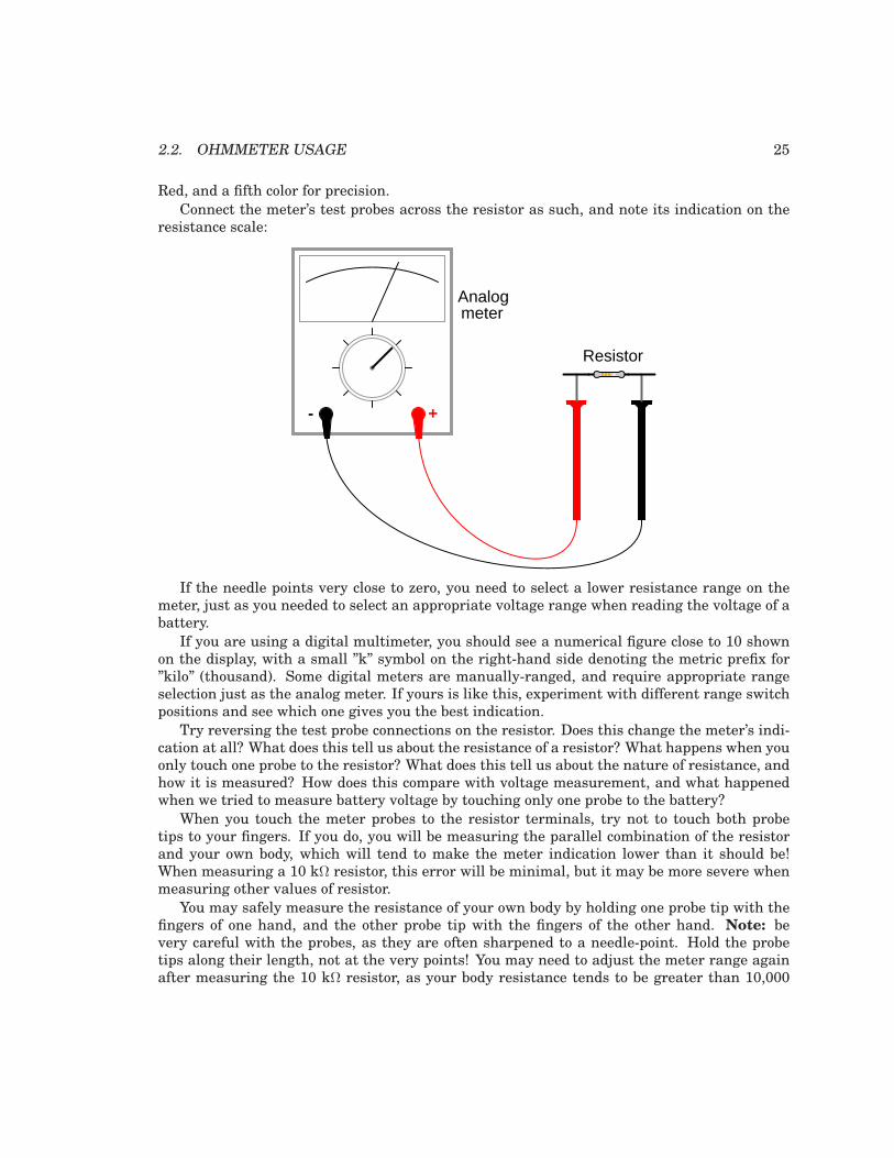
2.2. OHMMETER USAGE 25
Red, and a fifth color for precision.
Connect the meter’s test probes across the resistor as such, and note its indication on theresistance scale:
- +
Resistor
Analogmeter
If the needle points very close to zero, you need to select a lower resistance range on themeter, just as you needed to select an appropriate voltage range when reading the voltage of abattery.
If you are using a digital multimeter, you should see a numerical figure close to 10 shownon the display, with a small ”k” symbol on the right-hand side denoting the metric prefix for”kilo” (thousand). Some digital meters are manually-ranged, and require appropriate rangeselection just as the analog meter. If yours is like this, experiment with different range switchpositions and see which one gives you the best indication.
Try reversing the test probe connections on the resistor. Does this change the meter’s indi-cation at all? What does this tell us about the resistance of a resistor? What happens when youonly touch one probe to the resistor? What does this tell us about the nature of resistance, andhow it is measured? How does this compare with voltage measurement, and what happenedwhen we tried to measure battery voltage by touching only one probe to the battery?
When you touch the meter probes to the resistor terminals, try not to touch both probetips to your fingers. If you do, you will be measuring the parallel combination of the resistorand your own body, which will tend to make the meter indication lower than it should be!When measuring a 10 kΩ resistor, this error will be minimal, but it may be more severe whenmeasuring other values of resistor.
You may safely measure the resistance of your own body by holding one probe tip with thefingers of one hand, and the other probe tip with the fingers of the other hand. Note: bevery careful with the probes, as they are often sharpened to a needle-point. Hold the probetips along their length, not at the very points! You may need to adjust the meter range againafter measuring the 10 kΩ resistor, as your body resistance tends to be greater than 10,000

26 CHAPTER 2. BASIC CONCEPTS AND TEST EQUIPMENT
ohms hand-to-hand. Try wetting your fingers with water and re-measuring resistance with themeter. What impact does this have on the indication? Try wetting your fingers with saltwaterprepared using the glass of water and table salt, and re-measuring resistance. What impactdoes this have on your body’s resistance as measured by the meter?
Resistance is the measure of friction to electron flow through an object. The less resistancethere is between two points, the harder it is for electrons to move (flow) between those twopoints. Given that electric shock is caused by a large flow of electrons through a person’s body,and increased body resistance acts as a safeguard by making it more difficult for electrons toflow through us, what can we ascertain about electrical safety from the resistance readingsobtained with wet fingers? Does water increase or decrease shock hazard to people?
Measure the resistance of a rectifying diode with an analog meter. Try reversing the testprobe connections to the diode and re-measure resistance. What strikes you as being remark-able about the diode, especially in contrast to the resistor?
Take a piece of paper and draw a very heavy black mark on it with a pencil (not a pen!).Measure resistance on the black strip with your meter, placing the probe tips at each end ofthe mark like this:
- +
Paper
Mark made with pencil
Move the probe tips closer together on the black mark and note the change in resistancevalue. Does it increase or decrease with decreased probe spacing? If the results are inconsis-tent, you need to redraw the mark with more and heavier pencil strokes, so that it is consistent

2.2. OHMMETER USAGE 27
in its density. What does this teach you about resistance versus length of a conductive mate-rial?
Connect your meter to the terminals of a cadmium-sulphide (CdS) photocell and measurethe change in resistance created by differences in light exposure. Just as with the light-emitting diode (LED) of the voltmeter experiment, you may want to use alligator-clip jumperwires to make connection with the component, leaving your hands free to hold the photocell toa light source and/or change meter ranges:
- +
Light source
Photocell
Experiment with measuring the resistance of several different types of materials, just besure not to try measure anything that produces substantial voltage, like a battery. Suggestionsfor materials to measure are: fabric, plastic, wood, metal, clean water, dirty water, salt water,glass, diamond (on a diamond ring or other piece of jewelry), paper, rubber, and oil.

28 CHAPTER 2. BASIC CONCEPTS AND TEST EQUIPMENT
2.3 A very simple circuit
PARTS AND MATERIALS
• 6-volt battery
• 6-volt incandescent lamp
• Jumper wires
• Breadboard
• Terminal strip
From this experiment on, a multimeter is assumed to be necessary and will not be includedin the required list of parts and materials. In all subsequent illustrations, a digital multimeterwill be shown instead of an analog meter unless there is some particular reason to use ananalog meter. You are encouraged to use both types of meters to gain familiarity with theoperation of each in these experiments.
CROSS-REFERENCES
Lessons In Electric Circuits, Volume 1, chapter 1: ”Basic Concepts of Electricity”
LEARNING OBJECTIVES
• Essential configuration needed to make a circuit
• Normal voltage drops in an operating circuit
• Importance of continuity to a circuit
• Working definitions of ”open” and ”short” circuits
• Breadboard usage
• Terminal strip usage
SCHEMATIC DIAGRAM
Battery Lamp
ILLUSTRATION

2.3. A VERY SIMPLE CIRCUIT 29
BatteryLamp
+-
INSTRUCTIONS
This is the simplest complete circuit in this collection of experiments: a battery and anincandescent lamp. Connect the lamp to the battery as shown in the illustration, and the lampshould light, assuming the battery and lamp are both in good condition and they are matchedto one another in terms of voltage.
If there is a ”break” (discontinuity) anywhere in the circuit, the lamp will fail to light. It doesnot matter where such a break occurs! Many students assume that because electrons leave thenegative (-) side of the battery and continue through the circuit to the positive (+) side, that thewire connecting the negative terminal of the battery to the lamp is more important to circuitoperation than the other wire providing a return path for electrons back to the battery. This isnot true!
BatteryLamp
+- No light!
break in circuit
BatteryLamp
+- No light!
break in circuit

30 CHAPTER 2. BASIC CONCEPTS AND TEST EQUIPMENT
BatteryLamp
+- No light!
break in circuit
BatteryLamp
+- No light!
break in circuit
Using your multimeter set to the appropriate ”DC volt” range, measure voltage across thebattery, across the lamp, and across each jumper wire. Familiarize yourself with the normalvoltages in a functioning circuit.
Now, ”break” the circuit at one point and re-measure voltage between the same sets ofpoints, additionally measuring voltage across the break like this:

2.3. A VERY SIMPLE CIRCUIT 31
BatteryLamp
+- No light!
COMA
V
V A
AOFF
What voltages measure the same as before? What voltages are different since introducingthe break? How much voltage is manifest, or dropped across the break? What is the polarity
of the voltage drop across the break, as indicated by the meter?
Re-connect the jumper wire to the lamp, and break the circuit in another place. Measureall voltage ”drops” again, familiarizing yourself with the voltages of an ”open” circuit.
Construct the same circuit on a breadboard, taking care to place the lamp and wires intothe breadboard in such a way that continuity will be maintained. The example shown here isonly that: an example, not the only way to build a circuit on a breadboard:

32 CHAPTER 2. BASIC CONCEPTS AND TEST EQUIPMENT
+-
Breadboard
Experiment with different configurations on the breadboard, plugging the lamp into differ-ent holes. If you encounter a situation where the lamp refuses to light up and the connectingwires are getting warm, you probably have a situation known as a short circuit, where a lower-resistance path than the lamp bypasses current around the lamp, preventing enough voltagefrom being dropped across the lamp to light it up. Here is an example of a short circuit madeon a breadboard:

2.3. A VERY SIMPLE CIRCUIT 33
+-
Breadboard
No light!
"shorting"wire
Here is an example of an accidental short circuit of the type typically made by studentsunfamiliar with breadboard usage:
+-
Breadboard
No light!

34 CHAPTER 2. BASIC CONCEPTS AND TEST EQUIPMENT
Here there is no ”shorting” wire present on the breadboard, yet there is a short circuit, andthe lamp refuses to light. Based on your understanding of breadboard hole connections, canyou determine where the ”short” is in this circuit?
Short circuits are generally to be avoided, as they result in very high rates of electronflow, causing wires to heat up and battery power sources to deplete. If the power source issubstantial enough, a short circuit may cause heat of explosive proportions to manifest, causingequipment damage and hazard to nearby personnel. This is what happens when a tree limb”shorts” across wires on a power line: the limb – being composed of wet wood – acts as alow-resistance path to electric current, resulting in heat and sparks.
You may also build the battery/lamp circuit on a terminal strip: a length of insulatingmaterial with metal bars and screws to attach wires and component terminals to. Here is anexample of how this circuit might be constructed on a terminal strip:
+-
Terminalstrip

2.4. AMMETER USAGE 35
2.4 Ammeter usage
PARTS AND MATERIALS
• 6-volt battery
• 6-volt incandescent lamp
Basic circuit construction components such as breadboard, terminal strip, and jumper wiresare also assumed to be available from now on, leaving only components and materials uniqueto the project listed under ”Parts and Materials.”
CROSS-REFERENCES
Lessons In Electric Circuits, Volume 1, chapter 1: ”Basic Concepts of Electricity”
Lessons In Electric Circuits, Volume 1, chapter 8: ”DC Metering Circuits”
LEARNING OBJECTIVES
• How to measure current with a multimeter
• How to check a multimeter’s internal fuse
• Selection of proper meter range
SCHEMATIC DIAGRAM
Battery Lamp
A
Ammeter
ILLUSTRATION
36 CHAPTER 2. BASIC CONCEPTS AND TEST EQUIPMENT
BatteryLamp
+-
COMA
V
V A
AOFF
INSTRUCTIONS
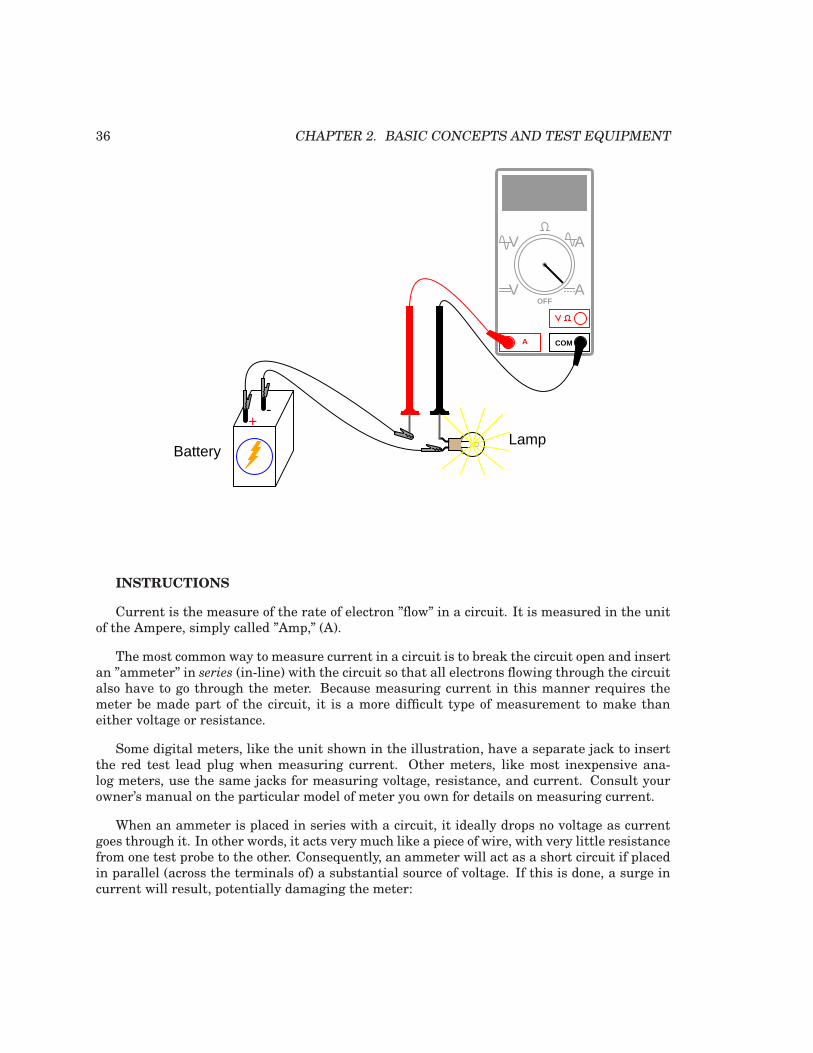
Current is the measure of the rate of electron ”flow” in a circuit. It is measured in the unitof the Ampere, simply called ”Amp,” (A).
The most common way to measure current in a circuit is to break the circuit open and insertan ”ammeter” in series (in-line) with the circuit so that all electrons flowing through the circuitalso have to go through the meter. Because measuring current in this manner requires themeter be made part of the circuit, it is a more difficult type of measurement to make thaneither voltage or resistance.
Some digital meters, like the unit shown in the illustration, have a separate jack to insertthe red test lead plug when measuring current. Other meters, like most inexpensive ana-log meters, use the same jacks for measuring voltage, resistance, and current. Consult yourowner’s manual on the particular model of meter you own for details on measuring current.
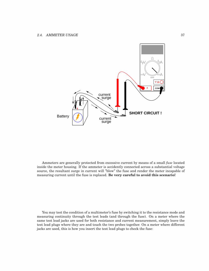
When an ammeter is placed in series with a circuit, it ideally drops no voltage as currentgoes through it. In other words, it acts very much like a piece of wire, with very little resistancefrom one test probe to the other. Consequently, an ammeter will act as a short circuit if placedin parallel (across the terminals of) a substantial source of voltage. If this is done, a surge incurrent will result, potentially damaging the meter:
2.4. AMMETER USAGE 37
Battery
+-
COMA
V
V A
AOFF
SHORT CIRCUIT !
current surge
current surge
Ammeters are generally protected from excessive current by means of a small fuse locatedinside the meter housing. If the ammeter is accidently connected across a substantial voltagesource, the resultant surge in current will ”blow” the fuse and render the meter incapable ofmeasuring current until the fuse is replaced. Be very careful to avoid this scenario!
You may test the condition of a multimeter’s fuse by switching it to the resistance mode andmeasuring continuity through the test leads (and through the fuse). On a meter where thesame test lead jacks are used for both resistance and current measurement, simply leave thetest lead plugs where they are and touch the two probes together. On a meter where differentjacks are used, this is how you insert the test lead plugs to check the fuse:

38 CHAPTER 2. BASIC CONCEPTS AND TEST EQUIPMENT
COMA
V
V A
AOFF
Internallocation of
fuse
Low resistanceindication = good fuse
High resistanceindication = "blown" fuse
touch probes together
Build the one-battery, one-lamp circuit using jumper wires to connect the battery to thelamp, and verify that the lamp lights up before connecting the meter in series with it. Then,break the circuit open at any point and connect the meter’s test probes to the two points ofthe break to measure current. As usual, if your meter is manually-ranged, begin by selectingthe highest range for current, then move the selector switch to lower range positions until thestrongest indication is obtained on the meter display without over-ranging it. If the meter in-dication is ”backwards,” (left motion on analog needle, or negative reading on a digital display),then reverse the test probe connections and try again. When the ammeter indicates a normalreading (not ”backwards”), electrons are entering the black test lead and exiting the red. Thisis how you determine direction of current using a meter.
For a 6-volt battery and a small lamp, the circuit current will be in the range of thousandthsof an amp, or milliamps. Digital meters often show a small letter ”m” in the right-hand side ofthe display to indicate this metric prefix.
Try breaking the circuit at some other point and inserting the meter there instead. Whatdo you notice about the amount of current measured? Why do you think this is?
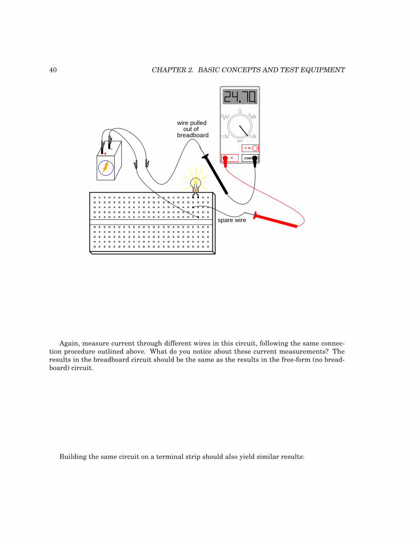
Re-construct the circuit on a breadboard like this:

2.4. AMMETER USAGE 39
+-
Breadboard
Students often get confused when connecting an ammeter to a breadboard circuit. How canthe meter be connected so as to intercept all the circuit’s current and not create a short circuit?One easy method that guarantees success is this:
• Identify what wire or component terminal you wish to measure current through.
• Pull that wire or terminal out of the breadboard hole. Leave it hanging in mid-air.
• Insert a spare piece of wire into the hole you just pulled the other wire or terminal out of.Leave the other end of this wire hanging in mid-air.
• Connect the ammeter between the two unconnected wire ends (the two that were hangingin mid-air). You are now assured of measuring current through the wire or terminalinitially identified.
40 CHAPTER 2. BASIC CONCEPTS AND TEST EQUIPMENT
+-
COMA
V
V A
AOFF
spare wire
wire pulledout of
breadboard
m
Again, measure current through different wires in this circuit, following the same connec-tion procedure outlined above. What do you notice about these current measurements? Theresults in the breadboard circuit should be the same as the results in the free-form (no bread-board) circuit.
Building the same circuit on a terminal strip should also yield similar results:

2.4. AMMETER USAGE 41
+-
Terminalstrip
COMA
V
V A
AOFF
m
The current figure of 24.70 milliamps (24.70 mA) shown in the illustrations is an arbitraryquantity, reasonable for a small incandescent lamp. If the current for your circuit is a differentvalue, that is okay, so long as the lamp is functioning when the meter is connected. If thelamp refuses to light when the meter is connected to the circuit, and the meter registers amuch greater reading, you probably have a short-circuit condition through the meter. If yourlamp refuses to light when the meter is connected in the circuit, and the meter registers zerocurrent, you’ve probably blown the fuse inside the meter. Check the condition of your meter’sfuse as described previously in this section and replace the fuse if necessary.

42 CHAPTER 2. BASIC CONCEPTS AND TEST EQUIPMENT
2.5 Ohm’s Law
PARTS AND MATERIALS
• Calculator (or pencil and paper for doing arithmetic)
• 6-volt battery
• Assortment of resistors between 1 KΩ and 100 kΩ in value
I’m purposely restricting the resistance values between 1 kΩ and 100 kΩ for the sake ofobtaining accurate voltage and current readings with your meter. With very low resistancevalues, the internal resistance of the ammeter has a significant impact on measurement accu-racy. Very high resistance values can cause problems for voltage measurement, the internalresistance of the voltmeter substantially changing circuit resistance when it is connected inparallel with a high-value resistor.
At the recommended resistance values, there will still be a small amount of measurementerror due to the ”impact” of the meter, but not enough to cause serious disagreement withcalculated values.
CROSS-REFERENCES
Lessons In Electric Circuits, Volume 1, chapter 2: ”Ohm’s Law”
LEARNING OBJECTIVES
• Voltmeter use
• Ammeter use
• Ohmmeter use
• Use of Ohm’s Law
SCHEMATIC DIAGRAM
Battery
A
Ammeter
Resistor V Voltmeter
ILLUSTRATION

2.5. OHM’S LAW 43
+-
Terminalstrip
COMA
V
V A
AOFF
Resistor
Ammeter
COMA
V
V A
AOFF
Voltmeter
INSTRUCTIONS
Select a resistor from the assortment, and measure its resistance with your multimeter setto the appropriate resistance range. Be sure not to hold the resistor terminals when measuringresistance, or else your hand-to-hand body resistance will influence the measurement! Recordthis resistance value for future use.
Build a one-battery, one-resistor circuit. A terminal strip is shown in the illustration, butany form of circuit construction is okay. Set your multimeter to the appropriate voltage rangeand measure voltage across the resistor as it is being powered by the battery. Record thisvoltage value along with the resistance value previously measured.
Set your multimeter to the highest current range available. Break the circuit and connectthe ammeter within that break, so it becomes a part of the circuit, in series with the batteryand resistor. Select the best current range: whichever one gives the strongest meter indication

44 CHAPTER 2. BASIC CONCEPTS AND TEST EQUIPMENT
without over-ranging the meter. If your multimeter is autoranging, of course, you need notbother with setting ranges. Record this current value along with the resistance and voltagevalues previously recorded.
Taking the measured figures for voltage and resistance, use the Ohm’s Law equation tocalculate circuit current. Compare this calculated figure with the measured figure for circuitcurrent:
Ohm’s Law
I = E
R
(solving for current)
Where,
I = Current in amps
E = Voltage in volts
R = Resistance in ohmsTaking the measured figures for voltage and current, use the Ohm’s Law equation to cal-
culate circuit resistance. Compare this calculated figure with the measured figure for circuitresistance:
Ohm’s Law
ER =
I
(solving for resistance)
Finally, taking the measured figures for resistance and current, use the Ohm’s Law equa-tion to calculate circuit voltage. Compare this calculated figure with the measured figure forcircuit voltage:
Ohm’s Law
E = IR
(solving for voltage)
There should be close agreement between all measured and all calculated figures. Anydifferences in respective quantities of voltage, current, or resistance are most likely due tometer inaccuracies. These differences should be rather small, no more than several percent.Some meters, of course, are more accurate than others!
Substitute different resistors in the circuit and re-take all resistance, voltage, and currentmeasurements. Re-calculate these figures and check for agreement with the experimental data(measured quantities). Also note the simple mathematical relationship between changes inresistor value and changes in circuit current. Voltage should remain approximately the samefor any resistor size inserted into the circuit, because it is the nature of a battery to maintainvoltage at a constant level.
2.6. NONLINEAR RESISTANCE 45
2.6 Nonlinear resistance
PARTS AND MATERIALS
• Calculator (or pencil and paper for doing arithmetic)
• 6-volt battery
• Low-voltage incandescent lamp (Radio Shack catalog # 272-1130 or equivalent)
CROSS-REFERENCES
Lessons In Electric Circuits, Volume 1, chapter 2: ”Ohm’s Law”
LEARNING OBJECTIVES
• Voltmeter use
• Ammeter use
• Ohmmeter use
• Use of Ohm’s Law
• Realization that some resistances are unstable!
• Scientific method
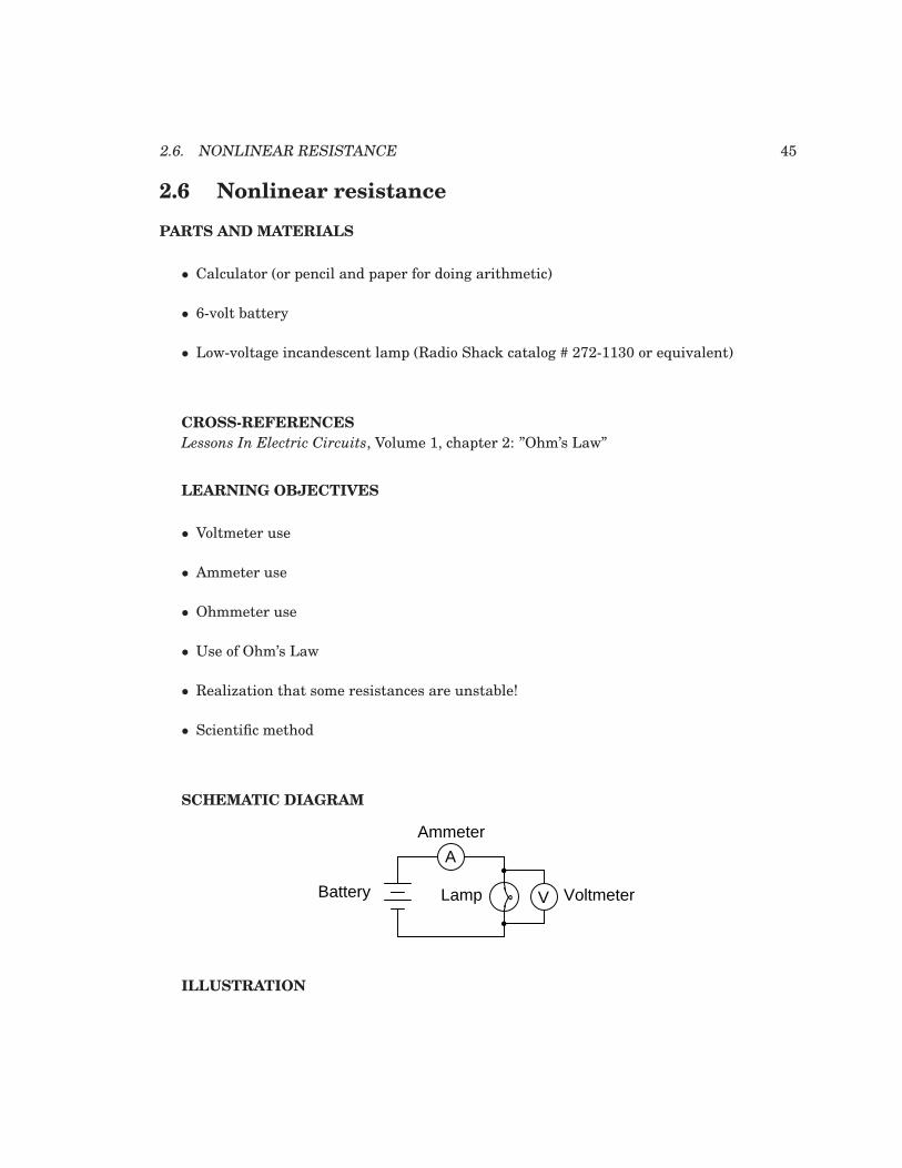
SCHEMATIC DIAGRAM
Battery
A
Ammeter
V VoltmeterLamp
ILLUSTRATION

46 CHAPTER 2. BASIC CONCEPTS AND TEST EQUIPMENT
+-
Terminalstrip
COMA
V
V A
AOFF
Ammeter
COMA
V
V A
AOFF
Voltmeter
Lamp
INSTRUCTIONS
Measure the resistance of the lamp with your multimeter. This resistance figure is due tothe thin metal ”filament” inside the lamp. It has substantially more resistance than a jumperwire, but less than any of the resistors from the last experiment. Record this resistance valuefor future use.
Build a one-battery, one-lamp circuit. Set your multimeter to the appropriate voltage rangeand measure voltage across the lamp as it is energized (lit). Record this voltage value alongwith the resistance value previously measured.
Set your multimeter to the highest current range available. Break the circuit and connectthe ammeter within that break, so it becomes a part of the circuit, in series with the batteryand lamp. Select the best current range: whichever one gives the strongest meter indicationwithout over-ranging the meter. If your multimeter is autoranging, of course, you need not

2.6. NONLINEAR RESISTANCE 47
bother with setting ranges. Record this current value along with the resistance and voltagevalues previously recorded.
Taking the measured figures for voltage and resistance, use the Ohm’s Law equation tocalculate circuit current. Compare this calculated figure with the measured figure for circuitcurrent:
Ohm’s Law
I = E
R
(solving for current)
Where,
I = Current in amps
E = Voltage in volts
R = Resistance in ohmsWhat you should find is a marked difference between measured current and calculated
current: the calculated figure is much greater. Why is this?To make things more interesting, try measuring the lamp’s resistance again, this time us-
ing a different model of meter. You will need to disconnect the lamp from the battery circuit inorder to obtain a resistance reading, because voltages outside of the meter interfere with re-sistance measurement. This is a general rule that should be remembered: measure resistanceonly on an unpowered component!
Using a different ohmmeter, the lamp will probably register as a different value of resis-tance. Usually, analog meters give higher lamp resistance readings than digital meters.
This behavior is very different from that of the resistors in the last experiment. Why? Whatfactor(s) might influence the resistance of the lamp filament, and how might those factors bedifferent between conditions of lit and unlit, or between resistance measurements taken withdifferent types of meters?
This problem is a good test case for the application of scientific method. Once you’ve thoughtof a possible reason for the lamp’s resistance changing between lit and unlit conditions, try toduplicate that cause by some other means. For example, if you think the lamp resistancemight change as it is exposed to light (its own light, when lit), and that this accounts for thedifference between the measured and calculated circuit currents, try exposing the lamp to anexternal source of light while measuring its resistance. If you measure substantial resistancechange as a result of light exposure, then your hypothesis has some evidential support. If not,then your hypothesis has been falsified, and another cause must be responsible for the changein circuit current.

48 CHAPTER 2. BASIC CONCEPTS AND TEST EQUIPMENT
2.7 Power dissipation
PARTS AND MATERIALS
• Calculator (or pencil and paper for doing arithmetic)
• 6 volt battery
• Two 1/4 watt resistors: 10 Ω and 330 Ω.
• Small thermometer
The resistor values need not be exact, but within five percent of the figures specified (+/- 0.5Ω for the 10 Ω resistor; +/- 16.5 Ω for the 330 Ω resistor). Color codes for 5% tolerance 10 Ω and330 Ω resistors are as follows: Brown, Black, Black, Gold (10, +/- 5%), and Orange, Orange,Brown, Gold (330, +/- 5%).
Do not use any battery size other than 6 volts for this experiment.The thermometer should be as small as possible, to facilitate rapid detection of heat pro-
duced by the resistor. I recommend a medical thermometer, the type used to take body temper-ature.
CROSS-REFERENCES
Lessons In Electric Circuits, Volume 1, chapter 2: ”Ohm’s Law”
LEARNING OBJECTIVES
• Voltmeter use
• Ammeter use
• Ohmmeter use
• Use of Joule’s Law
• Importance of component power ratings
• Significance of electrically common points
SCHEMATIC DIAGRAM
ILLUSTRATION

2.7. POWER DISSIPATION 49
+-
Caution: do not hold resistor withyour fingers while powered!
Thermometer
INSTRUCTIONS
Measure each resistor’s resistance with your ohmmeter, noting the exact values on a pieceof paper for later reference.
Connect the 330 Ω resistor to the 6 volt battery using a pair of jumper wires as shown inthe illustration. Connect the jumper wires to the resistor terminals before connecting the otherends to the battery. This will ensure your fingers are not touching the resistor when batterypower is applied.
You might be wondering why I advise no bodily contact with the powered resistor. Thisis because it will become hot when powered by the battery. You will use the thermometer tomeasure the temperature of each resistor when powered.
With the 330 Ω resistor connected to the battery, measure voltage with a voltmeter. Inmeasuring voltage, there is more than one way to obtain a proper reading. Voltage may bemeasured directly across the battery, or directly across the resistor. Battery voltage is the sameas resistor voltage in this circuit, since those two components share the same set of electricallycommon points: one side of the resistor is directly connected to one side of the battery, and theother side of the resistor is directly connected to the other side of the battery.

50 CHAPTER 2. BASIC CONCEPTS AND TEST EQUIPMENT
+-
COMA
V
V A
AOFF
electr
ically common
pointselectrically
commonpoints
All points of contact along the upper wire in the illustration (colored red) are electricallycommon to each other. All points of contact along the lower wire (colored black) are likewiseelectrically common to each other. Voltage measured between any point on the upper wire andany point on the lower wire should be the same. Voltage measured between any two common
points, however, should be zero.
Using an ammeter, measure current through the circuit. Again, there is no one ”correct”way to measure current, so long as the ammeter is placed within the flow-path of electronsthrough the resistor and not across a source of voltage. To do this, make a break in the circuit,and place the ammeter within that break: connect the two test probes to the two wire orterminal ends left open from the break. One viable option is shown in the following illustration:

2.7. POWER DISSIPATION 51
+-
COMA
V
V A
AOFF
Now that you’ve measured and recorded resistor resistance, circuit voltage, and circuit cur-rent, you are ready to calculate power dissipation. Whereas voltage is the measure of electrical”push” motivating electrons to move through a circuit, and current is the measure of electronflow rate, power is the measure ofwork-rate: how fast work is being done in the circuit. It takesa certain amount of work to push electrons through a resistance, and power is a description ofhow rapidly that work is taking place. In mathematical equations, power is symbolized by theletter ”P” and measured in the unit of the Watt (W).
Power may be calculated by any one of three equations – collectively referred to as Joule’sLaw – given any two out of three quantities of voltage, current, and resistance:
(solving for power)
P = IE
P = I2R
P =E2
R
Joule’s Law
Try calculating power in this circuit, using the three measured values of voltage, current,and resistance. Any way you calculate it, the power dissipation figure should be roughly thesame. Assuming a battery with 6.000 volts and a resistor of exactly 330 Ω, the power dissi-

52 CHAPTER 2. BASIC CONCEPTS AND TEST EQUIPMENT
pation will be 0.1090909 watts, or 109.0909 milli-watts (mW), to use a metric prefix. Sincethe resistor has a power rating of 1/4 watt (0.25 watts, or 250 mW), it is more than capable ofsustaining this level of power dissipation. Because the actual power level is almost half therated power, the resistor should become noticeably warm but it should not overheat. Touch thethermometer end to the middle of the resistor and see how warm it gets.
The power rating of any electrical component does not tell us how much power it will dis-sipate, but simply how much power it may dissipate without sustaining damage. If the actualamount of dissipated power exceeds a component’s power rating, that component will increasetemperature to the point of damage.
To illustrate, disconnect the 330 Ω resistor and replace it with the 10 Ω resistor. Again,avoid touching the resistor once the circuit is complete, as it will heat up rapidly. The safestway to do this is to disconnect one jumper wire from a battery terminal, then disconnect the330 Ω resistor from the two alligator clips, then connect the 10 Ω resistor between the two clips,and finally reconnect the jumper wire back to the battery terminal.
Caution: keep the 10 Ω resistor away from any flammable materials when it is
powered by the battery!
You may not have enough time to take voltage and current measurements before the re-sistor begins to smoke. At the first sign of distress, disconnect one of the jumper wires from abattery terminal to interrupt circuit current, and give the resistor a few moments to cool down.With power still disconnected, measure the resistor’s resistance with an ohmmeter and noteany substantial deviation from its original value. If the resistor still measures within +/- 5%of its advertised value (between 9.5 and 10.5 Ω), re-connect the jumper wire and let it smoke abit more.
What trend do you notice with the resistor’s value as it is damaged more and more byoverpowering? It is typical of resistors to fail with a greater-than-normal resistance whenoverheated. This is often a self-protective mode of failure, as an increased resistance resultsin less current and (generally) less power dissipation, cooling it down again. However, theresistor’s normal resistance value will not return if sufficiently damaged.
Performing some Joule’s Law calculations for resistor power again, we find that a 10 Ω
resistor connected to a 6 volt battery dissipates about 3.6 watts of power, about 14.4 times itsrated power dissipation. Little wonder it smokes so quickly after connection to the battery!

2.8. CIRCUIT WITH A SWITCH 53
2.8 Circuit with a switch
PARTS AND MATERIALS
• 6-volt battery
• Low-voltage incandescent lamp (Radio Shack catalog # 272-1130 or equivalent)
• Long lengths of wire, 22-gauge or larger
• Household light switch (these are readily available at any hardware store)
Household light switches are a bargain for students of basic electricity. They are readilyavailable, very inexpensive, and almost impossible to damage with battery power. Do not get”dimmer” switches, just the simple on-off ”toggle” variety used for ordinary household wall-mounted light controls.
CROSS-REFERENCES
Lessons In Electric Circuits, Volume 1, chapter 1: ”Basic Concepts of Electricity”
LEARNING OBJECTIVES
• Switch behavior
• Using an ohmmeter to check switch action
SCHEMATIC DIAGRAM
Switch
ILLUSTRATION

54 CHAPTER 2. BASIC CONCEPTS AND TEST EQUIPMENT
Switch
+-
INSTRUCTIONS
Build a one-battery, one-switch, one-lamp circuit as shown in the schematic diagram and inthe illustration. This circuit is most impressive when the wires are long, as it shows how theswitch is able to control circuit current no matter how physically large the circuit may be.
Measure voltage across the battery, across the switch (measure from one screw terminal toanother with the voltmeter), and across the lamp with the switch in both positions. When theswitch is turned off, it is said to be open, and the lamp will go out just the same as if a wirewere pulled loose from a terminal. As before, any break in the circuit at any location causesthe lamp to immediately de-energize (darken).

2.9. ELECTROMAGNETISM 55
2.9 Electromagnetism
PARTS AND MATERIALS
• 6-volt battery
• Magnetic compass
• Small permanent magnet
• Spool of 28-gauge magnet wire
• Large bolt, nail, or steel rod
• Electrical tape
Magnet wire is a term for thin-gauge copper wire with enamel insulation instead of rubberor plastic insulation. Its small size and very thin insulation allow for many ”turns” to be woundin a compact coil. You will need enough magnet wire to wrap hundreds of turns around thebolt, nail, or other rod-shaped steel form.
Be sure to select a bolt, nail, or rod that is magnetic. Stainless steel, for example, is non-magnetic and will not function for the purpose of an electromagnet coil! The ideal material forthis experiment is soft iron, but any commonly available steel will suffice.
CROSS-REFERENCES
Lessons In Electric Circuits, Volume 1, chapter 14: ”Magnetism and Electromagnetism”
LEARNING OBJECTIVES
• Application of the left-hand rule
• Electromagnet construction
SCHEMATIC DIAGRAM
ILLUSTRATION

56 CHAPTER 2. BASIC CONCEPTS AND TEST EQUIPMENT
+-
N
S
W E
Compass
Electromagnet(wire coil wrappedaround steel bar)
INSTRUCTIONS
Wrap a single layer of electrical tape around the steel bar (or bolt, or mail) to protect thewire from abrasion. Proceed to wrap several hundred turns of wire around the steel bar, mak-ing the coil as even as possible. It is okay to overlap wire, and it is okay to wrap in the samestyle that a fishing reel wraps line around the spool. The only rule you must follow is that allturns must be wrapped around the bar in the same direction (no reversing from clockwise tocounter-clockwise!). I find that a drill press works as a great tool for coil winding: clamp therod in the drill’s chuck as if it were a drill bit, then turn the drill motor on at a slow speed andlet it do the wrapping! This allows you to feed wire onto the rod in a very steady, even manner.
After you’ve wrapped several hundred turns of wire around the rod, wrap a layer or two ofelectrical tape over the wire coil to secure the wire in place. Scrape the enamel insulation offthe ends of the coil wires for connection to jumper leads, then connect the coil to a battery.
When electric current goes through the coil, it will produce a strong magnetic field: one”pole” at each end of the rod. This phenomenon is known as electromagnetism. The magneticcompass is used to identify the ”North” and ”South” poles of the electromagnet.
With the electromagnet energized (connected to the battery), place a permanent magnetnear one pole and note whether there is an attractive or repulsive force. Reverse the orienta-tion of the permanent magnet and note the difference in force.
Electromagnetism has many applications, including relays, electric motors, solenoids, door-bells, buzzers, computer printer mechanisms, andmagnetic media ”write” heads (tape recorders,disk drives).
You might notice a significant spark whenever the battery is disconnected from the elec-tromagnet coil: much greater than the spark produced if the battery is simply short-circuited.This spark is the result of a high-voltage surge created whenever current is suddenly inter-rupted through the coil. The effect is known as inductive ”kickback” and is capable of deliver-ing a small but harmless electric shock! To avoid receiving this shock, do not place your bodyacross the break in the circuit when de-energizing! Use one hand at a time when un-poweringthe coil and you’ll be perfectly safe. This phenomenon will be explored in greater detail in thenext chapter (DC Circuits).

2.10. ELECTROMAGNETIC INDUCTION 57
2.10 Electromagnetic induction
PARTS AND MATERIALS
• Electromagnet from previous experiment
• Permanent magnet
See previous experiment for instructions on electromagnet construction.
CROSS-REFERENCES
Lessons In Electric Circuits, Volume 1, chapter 14: ”Magnetism and Electromagnetism”
LEARNING OBJECTIVES
• Relationship between magnetic field strength and induced voltage
SCHEMATIC DIAGRAM
+V
-Voltmeter
ILLUSTRATION
Electromagnet
COMA
V
V A
AOFF
Magnet N
S
INSTRUCTIONS

58 CHAPTER 2. BASIC CONCEPTS AND TEST EQUIPMENT
Electromagnetic induction is the complementary phenomenon to electromagnetism. In-stead of producing a magnetic field from electricity, we produce electricity from a magneticfield. There is one important difference, though: whereas electromagnetism produces a steadymagnetic field from a steady electric current, electromagnetic induction requires motion be-tween the magnet and the coil to produce a voltage.
Connect the multimeter to the coil, and set it to the most sensitive DC voltage range avail-able. Move the magnet slowly to and from one end of the electromagnet, noting the polarityand magnitude of the induced voltage. Experiment with moving the magnet, and discover foryourself what factor(s) determine the amount of voltage induced. Try the other end of the coiland compare results. Try the other end of the permanent magnet and compare.
If using an analog multimeter, be sure to use long jumper wires and locate the meter faraway from the coil, as the magnetic field from the permanent magnet may affect the meter’soperation and produce false readings. Digital meters are unaffected by magnetic fields.

Chapter 3
DC CIRCUITS
Contents
3.1 Introduction . . . . . . . . . . . . . . . . . . . . . . . . . . . . . . . . . . . . . . 59
3.2 Series batteries . . . . . . . . . . . . . . . . . . . . . . . . . . . . . . . . . . . . 60
3.3 Parallel batteries . . . . . . . . . . . . . . . . . . . . . . . . . . . . . . . . . . . 63
3.4 Voltage divider . . . . . . . . . . . . . . . . . . . . . . . . . . . . . . . . . . . . 67
3.5 Current divider . . . . . . . . . . . . . . . . . . . . . . . . . . . . . . . . . . . . 78
3.6 Potentiometer as a voltage divider . . . . . . . . . . . . . . . . . . . . . . . . 87
3.7 Potentiometer as a rheostat . . . . . . . . . . . . . . . . . . . . . . . . . . . . 93
3.8 Precision potentiometer . . . . . . . . . . . . . . . . . . . . . . . . . . . . . . 99
3.9 Rheostat range limiting . . . . . . . . . . . . . . . . . . . . . . . . . . . . . . . 102
3.10 Thermoelectricity . . . . . . . . . . . . . . . . . . . . . . . . . . . . . . . . . . 109
3.11 Make your own multimeter . . . . . . . . . . . . . . . . . . . . . . . . . . . . 112
3.12 Sensitive voltage detector . . . . . . . . . . . . . . . . . . . . . . . . . . . . . 117
3.13 Potentiometric voltmeter . . . . . . . . . . . . . . . . . . . . . . . . . . . . . . 122
3.14 4-wire resistance measurement . . . . . . . . . . . . . . . . . . . . . . . . . . 127
3.15 A very simple computer . . . . . . . . . . . . . . . . . . . . . . . . . . . . . . . 131
3.16 Potato battery . . . . . . . . . . . . . . . . . . . . . . . . . . . . . . . . . . . . . 136
3.17 Capacitor charging and discharging . . . . . . . . . . . . . . . . . . . . . . . 138
3.18 Rate-of-change indicator . . . . . . . . . . . . . . . . . . . . . . . . . . . . . . 142
3.1 Introduction
”DC” stands for Direct Current, which can refer to either voltage or current in a constantpolarity or direction, respectively. These experiments are designed to introduce you to severalimportant concepts of electricity related to DC circuits.
59

60 CHAPTER 3. DC CIRCUITS
3.2 Series batteries
PARTS AND MATERIALS
• Two 6-volt batteries
• One 9-volt battery
Actually, any size batteries will suffice for this experiment, but it is recommended to haveat least two different voltages available to make it more interesting.
CROSS-REFERENCES
Lessons In Electric Circuits, Volume 1, chapter 5: ”Series and Parallel Circuits”
Lessons In Electric Circuits, Volume 1, chapter 11: ”Batteries and Power Systems”
LEARNING OBJECTIVES
• How to connect batteries to obtain different voltage levels
SCHEMATIC DIAGRAM
+V
-Voltmeter
+
+
-
-
ILLUSTRATION

3.2. SERIES BATTERIES 61
COMA
V
V A
AOFF
+-
+-
INSTRUCTIONS
Connecting components in series means to connect them in-line with each other, so thatthere is but a single path for electrons to flow through them all. If you connect batteries sothat the positive of one connects to the negative of the other, you will find that their respectivevoltages add. Measure the voltage across each battery individually as they are connected, thenmeasure the total voltage across them both, like this:

62 CHAPTER 3. DC CIRCUITS
COMA
V
V A
AOFF
+-
+-
COMA
V
V A
AOFF
+-
+-
COMA
V
V A
AOFF
+-
+-
Measuring first battery
Measuringsecond battery
Measuringtotal voltage
Try connecting batteries of different sizes in series with each other, for instance a 6-voltbattery with a 9-volt battery. What is the total voltage in this case? Try reversing the terminalconnections of just one of these batteries, so that they are opposing each other like this:
+V
-Voltmeter
+
+
-
-
Series-opposing
How does the total voltage compare in this situation to the previous one with both batteries”aiding?” Note the polarity of the total voltage as indicated by the voltmeter indication andtest probe orientation. Remember, if the meter’s digital indication is a positive number, the redprobe is positive (+) and the black probe negative (-); if the indication is a negative number,the polarity is ”backward” (red=negative, black=positive). Analog meters simply will not readproperly if reverse-connected, because the needle tries to move the wrong direction (left insteadof right). Can you predict what the overall voltage polarity will be, knowing the polarities ofthe individual batteries and their respective strengths?

3.3. PARALLEL BATTERIES 63
3.3 Parallel batteries
PARTS AND MATERIALS
• Four 6-volt batteries
• 12-volt light bulb, 25 or 50 watt
• Lamp socket
High-wattage 12-volt lamps may be purchased from recreational vehicle (RV) and boatingsupply stores. Common sizes are 25 watt and 50 watt. This lamp will be used as a ”heavy” loadfor your batteries (heavy load = one that draws substantial current).
A regular household (120 volt) lamp socket will work just fine for these low-voltage ”RV”lamps.
CROSS-REFERENCES
Lessons In Electric Circuits, Volume 1, chapter 5: ”Series and Parallel Circuits”Lessons In Electric Circuits, Volume 1, chapter 11: ”Batteries and Power Systems”
LEARNING OBJECTIVES
• Voltage source regulation
• Boosting current capacity through parallel connections
SCHEMATIC DIAGRAM
+ +
- -
+
-
+
-
ILLUSTRATION
+-
+-
+-
+-

64 CHAPTER 3. DC CIRCUITS
INSTRUCTIONS
Begin this experiment by connecting one 6-volt battery to the lamp. The lamp, designed tooperate on 12 volts, should glow dimly when powered by the 6-volt battery. Use your voltmeterto read voltage across the lamp like this:
+-
COMA
V
V A
AOFF
The voltmeter should register a voltage lower than the usual voltage of the battery. If youuse your voltmeter to read the voltage directly at the battery terminals, you will measure a lowvoltage there as well. Why is this? The large current drawn by the high-power lamp causes thevoltage at the battery terminals to ”sag” or ”droop,” due to voltage dropped across resistanceinternal to the battery.
We may overcome this problem by connecting batteries in parallel with each other, so thateach battery only has to supply a fraction of the total current demanded by the lamp. Parallelconnections involve making all the positive (+) battery terminals electrically common to eachother by connection through jumper wires, and all negative (-) terminals common to each otheras well. Add one battery at a time in parallel, noting the lamp voltage with the addition ofeach new, parallel-connected battery:

3.3. PARALLEL BATTERIES 65
+-
COMA
V
V A
AOFF
+-
+-
+-
. . . additional batteries . . .
There should also be a noticeable difference in light intensity as the voltage ”sag” is im-proved.
Try measuring the current of one battery and comparing it to the total current (light bulbcurrent). Shown here is the easiest way to measure single-battery current:
+-
+-
+-
+-
COMA
V
V A
AOFF
By breaking the circuit for just one battery, and inserting our ammeter within that break,we intercept the current of that one battery and are therefore able to measure it. Measuringtotal current involves a similar procedure: make a break somewhere in the path that totalcurrent must take, then insert the ammeter within than break:

66 CHAPTER 3. DC CIRCUITS
+-
+-
+-
+-
COMA
V
V A
AOFF
Note the difference in current between the single-battery and total measurements.To obtain maximum brightness from the light bulb, a series-parallel connection is required.
Two 6-volt batteries connected series-aiding will provide 12 volts. Connecting two of theseseries-connected battery pairs in parallel improves their current-sourcing ability for minimumvoltage sag:
+-
+-
+-
+-

3.4. VOLTAGE DIVIDER 67
3.4 Voltage divider
PARTS AND MATERIALS
• Calculator (or pencil and paper for doing arithmetic)
• 6-volt battery
• Assortment of resistors between 1 KΩ and 100 kΩ in value
I’m purposely restricting the resistance values between 1 kΩ and 100 kΩ for the sake ofobtaining accurate voltage and current readings with your meter. With very low resistancevalues, the internal resistance of the ammeter has a significant impact on measurement accu-racy. Very high resistance values may cause problems for voltage measurement, the internalresistance of the voltmeter substantially changing circuit resistance when it is connected inparallel with a high-value resistor.
CROSS-REFERENCES
Lessons In Electric Circuits, Volume 1, chapter 6: ”Divider Circuits and Kirchhoff ’s Laws”
LEARNING OBJECTIVES
• Voltmeter use
• Ammeter use
• Ohmmeter use
• Use of Ohm’s Law
• Use of Kirchhoff ’s Voltage Law (”KVL”)
• Voltage divider design
SCHEMATIC DIAGRAM
R1
R2
R3
+V
-Voltmeter

68 CHAPTER 3. DC CIRCUITS
ILLUSTRATION
+-
R1
R2
R3
Breadboard
+-
R1
R2
R3
Terminal strip

3.4. VOLTAGE DIVIDER 69
+-
R1 R2 R3
"Free-form" construction
INSTRUCTIONS
Shown here are three different methods of circuit construction: on a breadboard, on a termi-nal strip, and ”free-form.” Try building the same circuit each way to familiarize yourself withthe different construction techniques and their respective merits. The ”free-form” method –where all components are connected together with ”alligator-” style jumper wires – is the leastprofessional, but appropriate for a simple experiment such as this. Breadboard constructionis versatile and allows for high component density (many parts in a small space), but is quitetemporary. Terminal strips offer a much more permanent form of construction at the cost oflow component density.
Select three resistors from your resistor assortment and measure the resistance of each onewith an ohmmeter. Note these resistance values with pen and paper, for reference in yourcircuit calculations.
Connect the three resistors in series, and to the 6-volt battery, as shown in the illustrations.Measure battery voltage with a voltmeter after the resistors have been connected to it, notingthis voltage figure on paper as well. It is advisable to measure battery voltage while its pow-ering the resistor circuit because this voltage may differ slightly from a no-load condition. Wesaw this effect exaggerated in the ”parallel battery” experiment while powering a high-wattagelamp: battery voltage tends to ”sag” or ”droop” under load. Although this three-resistor circuitshould not present a heavy enough load (not enough current drawn) to cause significant volt-age ”sag,” measuring battery voltage under load is a good scientific practice because it providesmore realistic data.
Use Ohm’s Law (I=E/R) to calculate circuit current, then verify this calculated value bymeasuring current with an ammeter like this (”terminal strip” version of the circuit shown asan arbitrary choice in construction method):

70 CHAPTER 3. DC CIRCUITS
+-
R1
R2
R3
COMA
V
V A
AOFF
If your resistor values are indeed between 1 kΩ and 100 kΩ, and the battery voltage approx-imately 6 volts, the current should be a very small value, in the milliamp (mA) or microamp(µA) range. When you measure current with a digital meter, the meter may show the appro-priate metric prefix symbol (m or µ) in some corner of the display. These metric prefix telltalesare easy to overlook when reading the display of a digital meter, so pay close attention!
The measured value of current should agree closely with your Ohm’s Law calculation. Now,take that calculated value for current and multiply it by the respective resistances of eachresistor to predict their voltage drops (E=IR). Switch you multimeter to the ”voltage” mode andmeasure the voltage dropped across each resistor, verifying the accuracy of your predictions.Again, there should be close agreement between the calculated and measured voltage figures.
Each resistor voltage drop will be some fraction or percentage of the total voltage, hence thename voltage divider given to this circuit. This fractional value is determined by the resistanceof the particular resistor and the total resistance. If a resistor drops 50% of the total batteryvoltage in a voltage divider circuit, that proportion of 50% will remain the same as long as theresistor values are not altered. So, if the total voltage is 6 volts, the voltage across that resistorwill be 50% of 6, or 3 volts. If the total voltage is 20 volts, that resistor will drop 10 volts, or50% of 20 volts.
The next part of this experiment is a validation of Kirchhoff ’s Voltage Law. For this, youneed to identify each unique point in the circuit with a number. Points that are electricallycommon (directly connected to each other with insignificant resistance between) must bear thesame number. An example using the numbers 0 through 3 is shown here in both illustrative

3.4. VOLTAGE DIVIDER 71
and schematic form. In the illustration, I show how points in the circuit may be labeled withsmall pieces of tape, numbers written on the tape:
+-
R1
R2
R3
Terminal strip
0
0
0
1
3
3
3
2
12
R1
R2
R3
1
2
0 0
3 3
Using a digital voltmeter (this is important!), measure voltage drops around the loop formedby the points 0-1-2-3-0. Write on paper each of these voltages, along with its respective signas indicated by the meter. In other words, if the voltmeter registers a negative voltage suchas -1.325 volts, you should write that figure as a negative number. Do not reverse the meterprobe connections with the circuit to make the number read ”correctly.” Mathematical sign isvery significant in this phase of the experiment! Here is a sequence of illustrations showinghow to ”step around” the circuit loop, starting and ending at point 0:

72 CHAPTER 3. DC CIRCUITS
+-
R1
R2
R3
0
0
0
1
3
3
3
2
12
COMA
V
V A
AOFF
Measure voltage from 1 to 0
+-
R1
R2
R3
0
0
0
1
3
3
3
2
12
COMA
V
V A
AOFF
Measure voltage from to2 1

3.4. VOLTAGE DIVIDER 73
+-
R1
R2
R3
0
0
0
1
3
3
3
2
12
COMA
V
V A
AOFF
Measure voltage from to3 2
+-
R1
R2
R3
0
0
0
1
3
3
3
2
12
COMA
V
V A
AOFF
Measure voltage from to 30
Using the voltmeter to ”step” around the circuit in this manner yields three positive voltagefigures and one negative:

74 CHAPTER 3. DC CIRCUITS
R1
R2
R3
1
2
0 0
3 3
1-0
2-1
3-2
0-3
(+)
(+)
(+)
(-)
These figures, algebraically added (”algebraically” = respecting the signs of the numbers),should equal zero. This is the fundamental principle of Kirchhoff ’s Voltage Law: that thealgebraic sum of all voltage drops in a ”loop” add to zero.
It is important to realize that the ”loop” stepped around does not have to be the same paththat current takes in the circuit, or even a legitimate current path at all. The loop in which wetally voltage drops can be any collection of points, so long as it begins and ends with the samepoint. For example, we may measure and add the voltages in the loop 1-2-3-1, and they willform a sum of zero as well:
R1
R2
R3
1
2
0 0
3 3
2-1
3-2(+)
(+)
(-)1-3

3.4. VOLTAGE DIVIDER 75
+-
R1
R2
R3
0
0
0
1
3
3
3
2
12
COMA
V
V A
AOFF
Measure voltage from to2 1
+-
R1
R2
R3
0
0
0
1
3
3
3
2
12
COMA
V
V A
AOFF
Measure voltage from to3 2

76 CHAPTER 3. DC CIRCUITS
+-
R1
R2
R3
0
0
0
1
3
3
3
2
12
COMA
V
V A
AOFF
Measure voltage from to 31
Try stepping between any set of points, in any order, around your circuit and see for yourselfthat the algebraic sum always equals zero. This Law holds true no matter what the configura-tion of the circuit: series, parallel, series-parallel, or even an irreducible network.
Kirchhoff ’s Voltage Law is a powerful concept, allowing us to predict the magnitude andpolarity of voltages in a circuit by developing mathematical equations for analysis based on thetruth of all voltages in a loop adding up to zero. This experiment is intended to give empiricalevidence for and a deep understanding of Kirchhoff ’s Voltage Law as a general principle.
COMPUTER SIMULATION
Netlist (make a text file containing the following text, verbatim):Voltage dividerv1 3 0r1 3 2 5kr2 2 1 3kr3 1 0 2k.dc v1 6 6 1
* Voltages around 0-1-2-3-0 loop algebraically add to zero:.print dc v(1,0) v(2,1) v(3,2) v(0,3)
* Voltages around 1-2-3-1 loop algebraically add to zero:.print dc v(2,1) v(3,2) v(1,3).end
This computer simulation is based on the point numbers shown in the previous diagramsfor illustrating Kirchhoff ’s Voltage Law (points 0 through 3). Resistor values were chosen toprovide 50%, 30%, and 20% proportions of total voltage across R1, R2, and R3, respectively.Feel free to modify the voltage source value (in the ”.dc ” line, shown here as 6 volts), and/orthe resistor values.
When run, SPICE will print a line of text containing four voltage figures, then anotherline of text containing three voltage figures, along with lots of other text lines describing the

3.4. VOLTAGE DIVIDER 77
analysis process. Add the voltage figures in each line to see that the sum is zero.

78 CHAPTER 3. DC CIRCUITS
3.5 Current divider
PARTS AND MATERIALS
• Calculator (or pencil and paper for doing arithmetic)
• 6-volt battery
• Assortment of resistors between 1 KΩ and 100 kΩ in value
CROSS-REFERENCES
Lessons In Electric Circuits, Volume 1, chapter 6: ”Divider Circuits and Kirchhoff ’s Laws”
LEARNING OBJECTIVES
• Voltmeter use
• Ammeter use
• Ohmmeter use
• Use of Ohm’s Law
• Use of Kirchhoff ’s Current Law (KCL)
• Current divider design
SCHEMATIC DIAGRAM
R1 R2 R3
+A
-Ammeter
ILLUSTRATION

3.5. CURRENT DIVIDER 79
+-
R1 R2 R3
Breadboard
+-
R1 R2 R3
Terminalstrip
Normally, it is considered improper to secure more than two wires under a single terminalstrip screw. In this illustration, I show three wires joining at the top screw of the rightmostlug used on this strip. This is done for the ease of proving a concept (of current summing at acircuit node), and does not represent professional assembly technique.

80 CHAPTER 3. DC CIRCUITS
+-
R1 R2 R3
"Free-form" construction
Piece of stiff wire servesas a connection point
The non-professional nature of the ”free-form” construction method merits no further com-ment.
INSTRUCTIONS
Once again, I show different methods of constructing the same circuit: breadboard, terminalstrip, and ”free-form.” Experiment with all these construction formats and become familiarwith their respective advantages and disadvantages.
Select three resistors from your resistor assortment and measure the resistance of each onewith an ohmmeter. Note these resistance values with pen and paper, for reference in yourcircuit calculations.
Connect the three resistors in parallel to and each other, and with the 6-volt battery, asshown in the illustrations. Measure battery voltage with a voltmeter after the resistors havebeen connected to it, noting this voltage figure on paper as well. It is advisable to measurebattery voltage while its powering the resistor circuit because this voltage may differ slightlyfrom a no-load condition.
Measure voltage across each of the three resistors. What do you notice? In a series circuit,current is equal through all components at any given time. In a parallel circuit, voltage is thecommon variable between all components.
Use Ohm’s Law (I=E/R) to calculate current through each resistor, then verify this calcu-lated value by measuring current with a digital ammeter. Place the red probe of the ammeterat the point where the positive (+) ends of the resistors connect to each other and lift one re-sistor wire at a time, connecting the meter’s black probe to the lifted wire. In this manner,measure each resistor current, noting both the magnitude of the current and the polarity. Inthese illustrations, I show an ammeter used to measure the current through R1:

3.5. CURRENT DIVIDER 81
+-
R1 R2 R3
Breadboard
COMA
V
V A
AOFF

82 CHAPTER 3. DC CIRCUITS
+-
R1 R2 R3
Terminalstrip
COMA
V
V A
AOFF
Measure current for each of the three resistors, comparing with the current figures calcu-lated previously. With the digital ammeter connected as shown, all three indications should bepositive, not negative.
Now, measure total circuit current, keeping the ammeter’s red probe on the same pointof the circuit, but disconnecting the wire leading to the positive (+) side of the battery andtouching the black probe to it:

3.5. CURRENT DIVIDER 83
+-
R1 R2 R3
Breadboard
COMA
V
V A
AOFF

84 CHAPTER 3. DC CIRCUITS
+-
R1 R2 R3
Terminalstrip
COMA
V
V A
AOFF
Note both the magnitude and the sign of the current as indicated by the ammeter. Add thisfigure (algebraically) to the three resistor currents. What do you notice about the result thatis similar to the Kirchhoff ’s Voltage Law experiment? Kirchhoff ’s Current Law is to currents”summing” at a point (node) in a circuit, just as Kirchhoff ’s Voltage Law is to voltages addingin a series loop: in both cases, the algebraic sum is equal to zero.
This Law is also very useful in the mathematical analysis of circuits. Along with Kirchhoff ’sVoltage Law, it allows us to generate equations describing several variables in a circuit, whichmay then be solved using a variety of mathematical techniques.
Now consider the four current measurements as all positive numbers: the first three repre-senting the current through each resistor, and the fourth representing total circuit current asa positive sum of the three ”branch” currents. Each resistor (branch) current is a fraction, orpercentage, of the total current. This is why a parallel resistor circuit is often called a current
divider.
Disconnect the battery from the rest of the circuit, and measure resistance across the par-allel resistors. You may read total resistance across any of the individual resistors’ terminalsand obtain the same indication: it will be a value less than any of the individual resistor val-ues. This is often surprising to new students of electricity, that you read the exact same (total)resistance figure when connecting an ohmmeter across any one of a set of parallel-connectedresistors. It makes sense, though, if you consider the points in a parallel circuit in terms ofelectrical commonality. All parallel components are connected between two sets of electrically

3.5. CURRENT DIVIDER 85
common points. Since the meter cannot distinguish between points common to each other byway of direct connection, to read resistance across one resistor is to read the resistance of themall. The same is true for voltage, which is why battery voltage could be read across any one ofthe resistors as easily as it could be read across the battery terminals directly.
If you divide the battery voltage (previously measured) by this total resistance figure, youshould obtain a figure for total current (I=E/R) closely matching the measured figure.
The ratio of resistor current to total current is the same as the ratio of total resistance toindividual resistance. For example, if a 10 kΩ resistor is part of a current divider circuit witha total resistance of 1 kΩ, that resistor will conduct 1/10 of the total current, whatever valuethat current total happens to be.
COMPUTER SIMULATION
Schematic with SPICE node numbers:
R1 R2 R3V1
Vitotal Vir1 Vir2 Vir3
1
0 0 0 0
2 222
3 4 5
Ammeters in SPICE simulations are actually zero-voltage sources inserted in the paths ofelectron flow. You will notice the voltage sources Vir1, Vir2, and Vir3 are set to 0 volts in thenetlist. When electrons enter the negative side of one of these ”dummy” batteries and out thepositive, the battery’s current indication will be a positive number. In other words, these 0-voltsources are to be regarded as ammeters with the red probe on the long-line side of the batterysymbol and the black probe on the short-line side.
Netlist (make a text file containing the following text, verbatim):Current dividerv1 1 0r1 3 0 2kr2 4 0 3kr3 5 0 5kvitotal 2 1 dc 0vir1 2 3 dc 0vir2 2 4 dc 0vir3 2 5 dc 0.dc v1 6 6 1.print dc i(vitotal) i(vir1) i(vir2) i(vir3).end

86 CHAPTER 3. DC CIRCUITS
When run, SPICE will print a line of text containing four current figures, the first currentrepresenting the total as a negative quantity, and the other three representing currents forresistors R1, R2, and R3. When algebraically added, the one negative figure and the threepositive figures will form a sum of zero, as described by Kirchhoff ’s Current Law.

3.6. POTENTIOMETER AS A VOLTAGE DIVIDER 87
3.6 Potentiometer as a voltage divider
PARTS AND MATERIALS
• Two 6-volt batteries
• Carbon pencil ”lead” for a mechanical-style pencil
• Potentiometer, single turn, 5 kΩ to 50 kΩ, linear taper (Radio Shack catalog # 271-1714through 271-1716)
• Potentiometer, multi turn, 1 kΩ to 20 kΩ, (Radio Shack catalog # 271-342, 271-343, 900-8583, or 900-8587 through 900-8590)
Potentiometers are variable voltage dividers with a shaft or slide control for setting thedivision ratio. They are manufactured in panel-mount as well as breadboard (printed-circuitboard) mount versions. Any style of potentiometer will suffice for this experiment.
If you salvage a potentiometer from an old radio or other audio device, you will likely begetting what is called an audio taper potentiometer. These potentiometers exhibit a logarith-mic relationship between division ratio and shaft position. By contrast, a linear potentiometerexhibits a direct correlation between shaft position and voltage division ratio. I highly recom-mend a linear potentiometer for this experiment, and for most experiments in general.
CROSS-REFERENCES
Lessons In Electric Circuits, Volume 1, chapter 6: ”Divider Circuits and Kirchhoff ’s Laws”
LEARNING OBJECTIVES
• Voltmeter use
• Ohmmeter use
• Voltage divider design and function
• How voltages add in series
SCHEMATIC DIAGRAM
+V
-
Potentiometer
ILLUSTRATION

88 CHAPTER 3. DC CIRCUITS
+-
Pencil "lead"
COMA
V
V A
AOFF
+-
COMA
V
V A
AOFF
Potentiometer
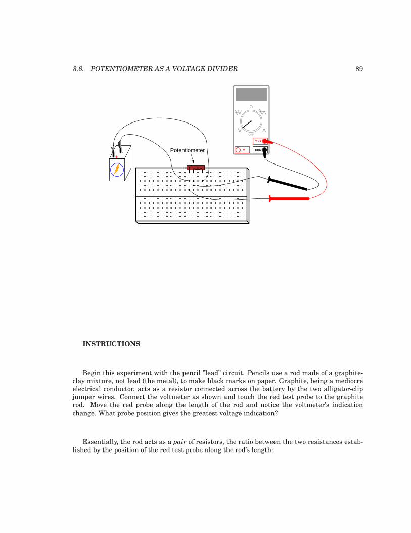
3.6. POTENTIOMETER AS A VOLTAGE DIVIDER 89
+-
COMA
V
V A
AOFF
Potentiometer
INSTRUCTIONS
Begin this experiment with the pencil ”lead” circuit. Pencils use a rod made of a graphite-clay mixture, not lead (the metal), to make black marks on paper. Graphite, being a mediocreelectrical conductor, acts as a resistor connected across the battery by the two alligator-clipjumper wires. Connect the voltmeter as shown and touch the red test probe to the graphiterod. Move the red probe along the length of the rod and notice the voltmeter’s indicationchange. What probe position gives the greatest voltage indication?
Essentially, the rod acts as a pair of resistors, the ratio between the two resistances estab-lished by the position of the red test probe along the rod’s length:

90 CHAPTER 3. DC CIRCUITS
+-
Pencil "lead"
equivalent to
Now, change the voltmeter connection to the circuit so as to measure voltage across the”upper resistor” of the pencil lead, like this:
+-
Pencil "lead"
COMA
V
V A
AOFF

3.6. POTENTIOMETER AS A VOLTAGE DIVIDER 91
Move the black test probe position along the length of the rod, noting the voltmeter indica-tion. Which position gives the greatest voltage drop for the meter to measure? Does this differfrom the previous arrangement? Why?
Manufactured potentiometers enclose a resistive strip inside a metal or plastic housing,and provide some kind of mechanism for moving a ”wiper” across the length of that resistivestrip. Here is an illustration of a rotary potentiometer’s construction:
Resistive strip
Wiper
Terminals
Rotary potentiometerconstruction
Some rotary potentiometers have a spiral resistive strip, and a wiper that moves axially asit rotates, so as to require multiple turns of the shaft to drive the wiper from one end of thepotentiometer’s range to the other. Multi-turn potentiometers are used in applications whereprecise setting is important.
Linear potentiometers also contain a resistive strip, the only difference being the wiper’sdirection of travel. Some linear potentiometers use a slide mechanism to move the wiper, whileothers a screw, to facilitate multiple-turn operation:
Resistive stripWiper
Terminals
Linear potentiometer construction
It should be noted that not all linear potentiometers have the same pin assignments. Onsome, the middle pin is the wiper.
Set up a circuit using a manufactured potentiometer, not the ”home-made” one made froma pencil lead. You may use any form of construction that is convenient.
Measure battery voltage while powering the potentiometer, and make note of this voltagefigure on paper. Measure voltage between the wiper and the potentiometer end connected tothe negative (-) side of the battery. Adjust the potentiometer mechanism until the voltmeter
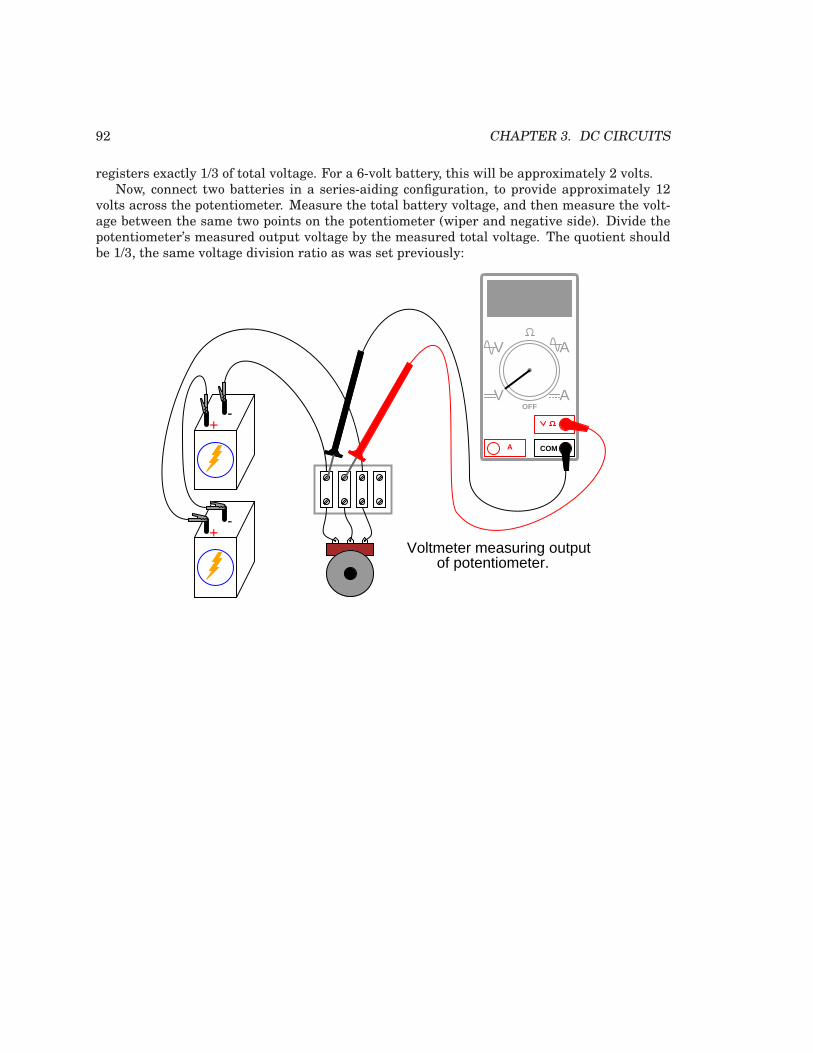
92 CHAPTER 3. DC CIRCUITS
registers exactly 1/3 of total voltage. For a 6-volt battery, this will be approximately 2 volts.Now, connect two batteries in a series-aiding configuration, to provide approximately 12
volts across the potentiometer. Measure the total battery voltage, and then measure the volt-age between the same two points on the potentiometer (wiper and negative side). Divide thepotentiometer’s measured output voltage by the measured total voltage. The quotient shouldbe 1/3, the same voltage division ratio as was set previously:
+-
COMA
V
V A
AOFF
+-
Voltmeter measuring outputof potentiometer.

3.7. POTENTIOMETER AS A RHEOSTAT 93
3.7 Potentiometer as a rheostat
PARTS AND MATERIALS
• 6 volt battery
• Potentiometer, single turn, 5 kΩ, linear taper (Radio Shack catalog # 271-1714)
• Small ”hobby” motor, permanent-magnet type (Radio Shack catalog # 273-223 or equiva-lent)
For this experiment, you will need a relatively low-value potentiometer, certainly not morethan 5 kΩ.
CROSS-REFERENCES
Lessons In Electric Circuits, Volume 1, chapter 2: ”Ohm’s Law”
LEARNING OBJECTIVES
• Rheostat use
• Wiring a potentiometer as a rheostat
• Simple motor speed control
• Use of voltmeter over ammeter to verify a continuous circuit
SCHEMATIC DIAGRAM
Mtr
ILLUSTRATION

94 CHAPTER 3. DC CIRCUITS
+-
Potentiometer
Motor
optional
INSTRUCTIONS
Potentiometers find their most sophisticated application as voltage dividers, where shaftposition determines a specific voltage division ratio. However, there are applications where wedon’t necessarily need a variable voltage divider, but merely a variable resistor: a two-terminaldevice. Technically, a variable resistor is known as a rheostat, but potentiometers can be madeto function as rheostats quite easily.
In its simplest configuration, a potentiometer may be used as a rheostat by simply usingthe wiper terminal and one of the other terminals, the third terminal left unconnected andunused:
Mtr

3.7. POTENTIOMETER AS A RHEOSTAT 95
+-
Potentiometer
Motor
Moving the potentiometer control in the direction that brings the wiper closest to the otherused terminal results in a lower resistance. The direction of motion required to increase ordecrease resistance may be changed by using a different set of terminals:
Resistive strip
Wiper
Less resistance when turned clockwise
Resistive strip
Wiper
More resistance when turned clockwise
Be careful, though, that you don’t use the two outer terminals, as this will result in no
change in resistance as the potentiometer shaft is turned. In other words, it will no longerfunction as a variable resistance:

96 CHAPTER 3. DC CIRCUITS
No resistance change when wiper moves!
Build the circuit as shown in the schematic and illustration, using just two terminals onthe potentiometer, and see how motor speed may be controlled by adjusting shaft position.Experiment with different terminal connections on the potentiometer, noting the changes inmotor speed control. If your potentiometer has a high resistance (as measured between thetwo outer terminals), the motor might not move at all until the wiper is brought very close tothe connected outer terminal.
As you can see, motor speed may be made variable using a series-connected rheostat tochange total circuit resistance and limit total current. This simple method of motor speedcontrol, however, is inefficient, as it results in substantial amounts of power being dissipated(wasted) by the rheostat. A much more efficient means of motor control relies on fast ”pulsing”of power to the motor, using a high-speed switching device such as a transistor. A similarmethod of power control is used in household light ”dimmer” switches. Unfortunately, thesetechniques are much too sophisticated to explore at this point in the experiments.
When a potentiometer is used as a rheostat, the ”unused” terminal is often connected to thewiper terminal, like this:
Mtr
At first, this seems rather pointless, as it has no impact on resistance control. You mayverify this fact for yourself by inserting another wire in your circuit and comparing motorbehavior before and after the change:

3.7. POTENTIOMETER AS A RHEOSTAT 97
+-
Potentiometer
Motor
add wire
If the potentiometer is in good working order, this additional wire makes no differencewhatsoever. However, if the wiper ever loses contact with the resistive strip inside the poten-tiometer, this connection ensures the circuit does not completely open: that there will still bea resistive path for current through the motor. In some applications, this may be an impor-tant. Old potentiometers tend to suffer from intermittent losses of contact between the wiperand the resistive strip, and if a circuit cannot tolerate the complete loss of continuity (infiniteresistance) created by this condition, that ”extra” wire provides a measure of protection bymaintaining circuit continuity.
You may simulate such a wiper contact ”failure” by disconnecting the potentiometer’s mid-dle terminal from the terminal strip, measuring voltage across the motor to ensure there isstill power getting to it, however small:

98 CHAPTER 3. DC CIRCUITS
+-
break connection
COMA
V
V A
AOFF
It would have been valid to measure circuit current instead of motor voltage to verify acompleted circuit, but this is a safer method because it does not involve breaking the circuitto insert an ammeter in series. Whenever an ammeter is used, there is risk of causing a shortcircuit by connecting it across a substantial voltage source, possibly resulting in instrumentdamage or personal injury. Voltmeters lack this inherent safety risk, and so whenever a voltagemeasurement may be made instead of a current measurement to verify the same thing, it isthe wiser choice.

3.8. PRECISION POTENTIOMETER 99
3.8 Precision potentiometer
PARTS AND MATERIALS
• Two single-turn, linear-taper potentiometers, 5 kΩ each (Radio Shack catalog # 271-1714)
• One single-turn, linear-taper potentiometer, 50 kΩ (Radio Shack catalog # 271-1716)
• Plastic or metal mounting box
• Three ”banana” jack style binding posts, or other terminal hardware, for connection topotentiometer circuit (Radio Shack catalog # 274-662 or equivalent)
This is a project useful to those who want a precision potentiometer without spending a lotof money. Ordinarily, multi-turn potentiometers are used to obtain precise voltage division ra-tios, but a cheaper alternative exists using multiple, single-turn (sometimes called ”3/4-turn”)potentiometers connected together in a compound divider network.
Because this is a useful project, I recommend building it in permanent form using someform of project enclosure. Suppliers such as Radio Shack offer nice project boxes, but boxespurchased at a general hardware store are much less expensive, if a bit ugly. The ultimatein low cost for a new box are the plastic boxes sold as light switch and receptacle boxes forhousehold electrical wiring.
”Banana” jacks allow for the temporary connection of test leads and jumper wires equippedwith matching ”banana” plug ends. Most multimeter test leads have this style of plug forinsertion into the meter jacks. Banana plugs are so named because of their oblong appearanceformed by spring steel strips, which maintain firm contact with the jack walls when inserted.Some banana jacks are called binding posts because they also allow plain wires to be firmlyattached. Binding posts have screw-on sleeves that fit over a metal post. The sleeve is used as anut to secure a wire wrapped around the post, or inserted through a perpendicular hole drilledthrough the post. A brief inspection of any binding post will clarify this verbal description.
CROSS-REFERENCES
Lessons In Electric Circuits, Volume 1, chapter 6: ”Divider Circuits and Kirchhoff ’s Laws”
LEARNING OBJECTIVES
• Soldering practice
• Potentiometer function and operation
SCHEMATIC DIAGRAM

100 CHAPTER 3. DC CIRCUITS
R1
R2
R3
+V
-
5 kΩ
5 kΩ
50kΩ
ILLUSTRATION
+- COMA
V
V A
AOFF
R1
R2
R35 kΩ
5 kΩ50 kΩ
INSTRUCTIONS
It is essential that the connecting wires be soldered to the potentiometer terminals, nottwisted or taped. Since potentiometer action is dependent on resistance, the resistance ofall wiring connections must be carefully controlled to a bare minimum. Soldering ensures acondition of low resistance between joined conductors, and also provides very good mechanicalstrength for the connections.
When the circuit is assembled, connect a 6-volt battery to the outer two binding posts.Connect a voltmeter between the ”wiper” post and the battery’s negative (-) terminal. Thisvoltmeter will measure the ”output” of the circuit.
The circuit works on the principle of compressed range: the voltage output range of thiscircuit available by adjusting potentiometer R3 is restricted between the limits set by poten-tiometers R1 and R2. In other words, if R1 and R2 were set to output 5 volts and 3 volts,

3.8. PRECISION POTENTIOMETER 101
respectively, from a 6-volt battery, the range of output voltages obtainable by adjusting R3
would be restricted from 3 to 5 volts for the full rotation of that potentiometer. If only a singlepotentiometer were used instead of this three-potentiometer circuit, full rotation would pro-duce an output voltage from 0 volts to full battery voltage. The ”range compression” affordedby this circuit allows for more precise voltage adjustment than would be normally obtainableusing a single potentiometer.
Operating this potentiometer network is more complex than using a single potentiometer.To begin, turn the R3 potentiometer fully clockwise, so that its wiper is in the full ”up” positionas referenced to the schematic diagram (electrically ”closest” to R1’s wiper terminal). Adjustpotentiometer R1 until the upper voltage limit is reached, as indicated by the voltmeter.
Turn the R3 potentiometer fully counter-clockwise, so that its wiper is in the full ”down”position as referenced to the schematic diagram (electrically ”closest” to R2’s wiper terminal).Adjust potentiometer R2 until the lower voltage limit is reached, as indicated by the voltmeter.
When either the R1 or the R2 potentiometer is adjusted, it interferes with the prior settingof the other. In other words, if R1 is initially adjusted to provide an upper voltage limit of 5.000volts from a 6 volt battery, and then R2 is adjusted to provide some lower limit voltage differentfrom what it was before, R1 will no longer be set to 5.000 volts.
To obtain precise upper and lower voltage limits, turn R3 fully clockwise to read and adjustthe voltage of R1, then turn R3 fully counter-clockwise to read and adjust the voltage of R2,repeating as necessary.
Technically, this phenomenon of one adjustment affecting the other is known as interaction,and it is usually undesirable due to the extra effort required to set and re-set the adjustments.The reason that R1 and R2 were specified as 10 times less resistance than R3 is to minimize thiseffect. If all three potentiometers were of equal resistance value, the interaction between R1
and R2 would be more severe, though manageable with patience. Bear in mind that the upperand lower voltage limits need not be set precisely in order for this circuit to achieve its goal ofincreased precision. So long as R3’s adjustment range is compressed to some lesser value thanfull battery voltage, we will enjoy greater precision than a single potentiometer could provide.
Once the upper and lower voltage limits have been set, potentiometer R3 may be adjustedto produce an output voltage anywhere between those limits.
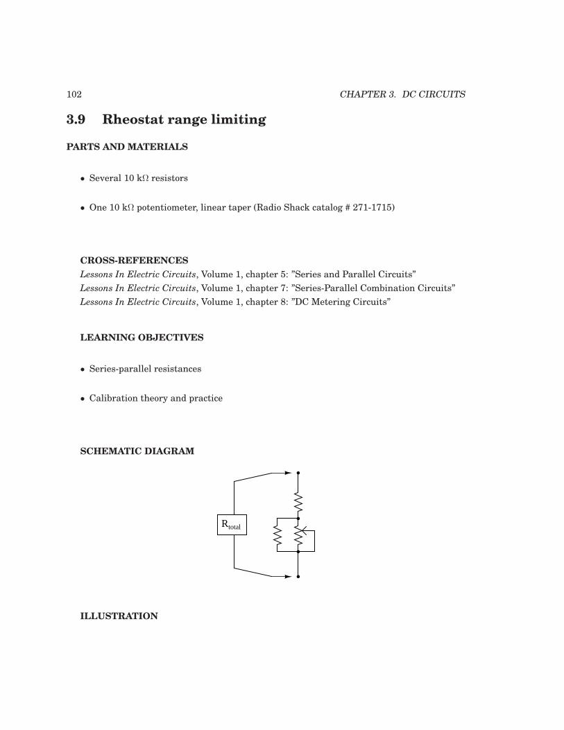
102 CHAPTER 3. DC CIRCUITS
3.9 Rheostat range limiting
PARTS AND MATERIALS
• Several 10 kΩ resistors
• One 10 kΩ potentiometer, linear taper (Radio Shack catalog # 271-1715)
CROSS-REFERENCES
Lessons In Electric Circuits, Volume 1, chapter 5: ”Series and Parallel Circuits”
Lessons In Electric Circuits, Volume 1, chapter 7: ”Series-Parallel Combination Circuits”
Lessons In Electric Circuits, Volume 1, chapter 8: ”DC Metering Circuits”
LEARNING OBJECTIVES
• Series-parallel resistances
• Calibration theory and practice
SCHEMATIC DIAGRAM
Rtotal
ILLUSTRATION

3.9. RHEOSTAT RANGE LIMITING 103
COMA
V
V A
AOFF
INSTRUCTIONS
This experiment explores the different resistance ranges obtainable from combining fixed-value resistors with a potentiometer connected as a rheostat. To begin, connect a 10 kΩ poten-tiometer as a rheostat with no other resistors connected. Adjusting the potentiometer throughits full range of travel should result in a resistance that varies smoothly from 0 Ω to 10,000 Ω:

104 CHAPTER 3. DC CIRCUITS
COMA
V
V A
AOFF
Suppose we wanted to elevate the lower end of this resistance range so that we had anadjustable range from 10 kΩ to 20 kΩ with a full sweep of the potentiometer’s adjustment. Thiscould be easily accomplished by adding a 10 kΩ resistor in series with the potentiometer. Addone to the circuit as shown and re-measure total resistance while adjusting the potentiometer:

3.9. RHEOSTAT RANGE LIMITING 105
COMA
V
V A
AOFF
A shift in the low end of an adjustment range is called a zero calibration, in metrologicalterms. With the addition of a series 10 kΩ resistor, the ”zero point” was shifted upward by10,000 Ω. The difference between high and low ends of a range – called the span of the circuit– has not changed, though: a range of 10 kΩ to 20 kΩ has the same 10,000 Ω span as a rangeof 0 Ω to 10 kΩ. If we wish to shift the span of this rheostat circuit as well, we must changethe range of the potentiometer itself. We could replace the potentiometer with one of anothervalue, or we could simulate a lower-value potentiometer by placing a resistor in parallel withit, diminishing its maximum obtainable resistance. This will decrease the span of the circuitfrom 10 kΩ to something less.
Add a 10 kΩ resistor in parallel with the potentiometer, to reduce the span to one-half of itsformer value: from 10 KΩ to 5 kΩ. Now the calibrated resistance range of this circuit will be10 kΩ to 15 kΩ:

106 CHAPTER 3. DC CIRCUITS
COMA
V
V A
AOFF
There is nothing we can do to increase the span of this rheostat circuit, short of replacingthe potentiometer with another of greater total resistance. Adding resistors in parallel canonly decrease the span. However, there is no such restriction with calibrating the zero point ofthis circuit, as it began at 0 Ω and may be made as great as we wish by adding resistance inseries.
A multitude of resistance ranges may be obtained using only 10 KΩ fixed-value resistors, ifwe are creative with series-parallel combinations of them. For instance, we can create a rangeof 7.5 kΩ to 10 kΩ by building the following circuit:

3.9. RHEOSTAT RANGE LIMITING 107
All resistors = 10 kΩ
Rtotal
2.5 kΩ 5 kΩ0 to 2.5 kΩ
COMA
V
V A
AOFF
Creating a custom resistance range from fixed-value resistors and a potentiometer is avery useful technique for producing precise resistances required for certain circuits, especiallymeter circuits. In many electrical instruments – multimeters especially – resistance is thedetermining factor for the instrument’s range of measurement. If an instrument’s internalresistance values are not precise, neither will its indications be. Finding a fixed-value resistor

108 CHAPTER 3. DC CIRCUITS
of just the right resistance for placement in an instrument circuit design is unlikely, so cus-tom resistance ”networks” may need to be built to provide the desired resistance. Having apotentiometer as part of the resistor network provides a means of correction if the network’sresistance should ”drift” from its original value. Designing the network for minimum spanensures that the potentiometer’s effect will be small, so that precise adjustment is possible andso that accidental movement of its mechanism will not result in severe calibration errors.
Experiment with different resistor ”networks” and note the effects on total resistance range.

3.10. THERMOELECTRICITY 109
3.10 Thermoelectricity
PARTS AND MATERIALS
• Length of bare (uninsulated) copper wire
• Length of bare (uninsulated) iron wire
• Candle
• Ice cubes
Iron wire may be obtained from a hardware store. If some cannot be found, aluminum wirealso works.
CROSS-REFERENCES
Lessons In Electric Circuits, Volume 1, chapter 9: ”Electrical Instrumentation Signals”
LEARNING OBJECTIVES
• Thermocouple function and purpose
SCHEMATIC DIAGRAM
+V
-
Thermocouple Voltmeter
ILLUSTRATION

110 CHAPTER 3. DC CIRCUITS
Candle
iron wire
copper wire
COMA
V
V A
AOFF
INSTRUCTIONS
Twist one end of the iron wire together with one end of the copper wire. Connect the freeends of these wires to respective terminals on a terminal strip. Set your voltmeter to its mostsensitive range and connect it to the terminals where the wires attach. The meter shouldindicate nearly zero voltage.
What you have just constructed is a thermocouple: a device which generates a small voltageproportional to the temperature difference between the tip and the meter connection points.When the tip is at a temperature equal to the terminal strip, there will be no voltage produced,and thus no indication seen on the voltmeter.
Light a candle and insert the twisted-wire tip into the flame. You should notice an indicationon your voltmeter. Remove the thermocouple tip from the flame and let cool until the voltmeterindication is nearly zero again. Now, touch the thermocouple tip to an ice cube and note thevoltage indicated by the meter. Is it a greater or lesser magnitude than the indication obtainedwith the flame? How does the polarity of this voltage compare with that generated by theflame?
After touching the thermocouple tip to the ice cube, warm it by holding it between yourfingers. It may take a short while to reach body temperature, so be patient while observing thevoltmeter’s indication.

3.10. THERMOELECTRICITY 111
A thermocouple is an application of the Seebeck effect: the production of a small voltageproportional to a temperature gradient along the length of a wire. This voltage is dependentupon the magnitude of the temperature difference and the type of wire. Directly measuringthe Seebeck voltage produced along a length of continuous wire from a temperature gradientis quite difficult, and so will not be attempted in this experiment.
Thermocouples, being made of two dissimilar metals joined at one end, produce a voltageproportional to the temperature of the junction. The temperature gradient along both wiresresulting from a constant temperature at the junction produces different Seebeck voltagesalong those wires’ lengths, because the wires are made of different metals. The resultantvoltage between the two free wire ends is the difference between the two Seebeck voltages:
iron wire voltage
copper wire voltage
ResultantvoltageHOT COOL
Thermocouples are widely used as temperature-sensing devices because the mathemati-cal relationship between temperature difference and resultant voltage is both repeatable andfairly linear. By measuring voltage, it is possible to infer temperature. Different ranges oftemperature measurement are possible by selecting different metal pairs to be joined together.

112 CHAPTER 3. DC CIRCUITS
3.11 Make your own multimeter
PARTS AND MATERIALS
• Sensitive meter movement (Radio Shack catalog # 22-410)
• Selector switch, single-pole, multi-throw, break-before-make (Radio Shack catalog # 275-1386 is a 2-pole, 6-position unit that works well)
• Multi-turn potentiometers, PCB mount (Radio Shack catalog # 271-342 and 271-343 are15-turn, 1 kΩ and 10 kΩ ”trimmer” units, respectively)
• Assorted resistors, preferably high-precision metal film or wire-wound types (Radio Shackcatalog # 271-309 is an assortment of metal-film resistors, +/- 1% tolerance)
• Plastic or metal mounting box
• Three ”banana” jack style binding posts, or other terminal hardware, for connection topotentiometer circuit (Radio Shack catalog # 274-662 or equivalent)
The most important and expensive component in a meter is the movement: the actualneedle-and-scale mechanism whose task it is to translate an electrical current into mechanicaldisplacement where it may be visually interpreted. The ideal meter movement is physicallylarge (for ease of viewing) and as sensitive as possible (requires minimal current to producefull-scale deflection of the needle). High-quality meter movements are expensive, but RadioShack carries some of acceptable quality that are reasonably priced. The model recommendedin the parts list is sold as a voltmeter with a 0-15 volt range, but is actually a milliammeterwith a range (”multiplier”) resistor included separately.
It may be cheaper to purchase an inexpensive analog meter and disassemble it for the metermovement alone. Although the thought of destroying a working multimeter in order to haveparts to make your own may sound counter-productive, the goal here is learning, not meterfunction.
I cannot specify resistor values for this experiment, as these depend on the particular metermovement and measurement ranges chosen. Be sure to use high-precision fixed-value resis-tors rather than carbon-composition resistors. Even if you happen to find carbon-compositionresistors of just the right value(s), those values will change or ”drift” over time due to agingand temperature fluctuations. Of course, if you don’t care about the long-term stability of thismeter but are building it just for the learning experience, resistor precision matters little.
CROSS-REFERENCES
Lessons In Electric Circuits, Volume 1, chapter 8: ”DC Metering Circuits”
LEARNING OBJECTIVES
• Voltmeter design and use
• Ammeter design and use
• Rheostat range limiting

3.11. MAKE YOUR OWN MULTIMETER 113
• Calibration theory and practice
• Soldering practice
SCHEMATIC DIAGRAM
+-
"Common"jack
Rshunt
Rmultiplier1
Rmultiplier2
Rmultiplier3
VV
V
AOff
A
mA
V/mA
Movement
Rmultiplier
"Rmultiplier" resistors are actually rheostat networks
ILLUSTRATION

114 CHAPTER 3. DC CIRCUITS
- +
Selectorswitch
Rshunt
Common
A
V/mA
Metermovement
INSTRUCTIONS
First, you need to determine the characteristics of your meter movement. Most importantis to know the full scale deflection in milliamps or microamps. To determine this, connectthe meter movement, a potentiometer, battery, and digital ammeter in series. Adjust the po-tentiometer until the meter movement is deflected exactly to full-scale. Read the ammeter’sdisplay to find the full-scale current value:

3.11. MAKE YOUR OWN MULTIMETER 115
Metermovement
+-
Potentiometer
COMA
V
V A
AOFF
- +
Be very careful not to apply too much current to the meter movement, as movements arevery sensitive devices and easily damaged by overcurrent. Most meter movements have full-scale deflection current ratings of 1 mA or less, so choose a potentiometer value high enoughto limit current appropriately, and begin testing with the potentiometer turned to maximumresistance. The lower the full-scale current rating of a movement, the more sensitive it is.
After determining the full-scale current rating of your meter movement, you must accu-rately measure its internal resistance. To do this, disconnect all components from the previ-ous testing circuit and connect your digital ohmmeter across the meter movement terminals.Record this resistance figure along with the full-scale current figure obtained in the last proce-dure.
Perhaps the most challenging portion of this project is determining the proper range resis-tance values and implementing those values in the form of rheostat networks. The calculationsare outlined in chapter 8 of volume 1 (”Metering Circuits”), but an example is given here. Sup-pose your meter movement had a full-scale rating of 1 mA and an internal resistance of 400Ω. If we wanted to determine the necessary range resistance (”Rmultiplier”) to give this move-ment a range of 0 to 15 volts, we would have to divide 15 volts (total applied voltage) by 1 mA(full-scale current) to obtain the total probe-to-probe resistance of the voltmeter (R=E/I). Forthis example, that total resistance is 15 kΩ. From this total resistance figure, we subtract themovement’s internal resistance, leaving 14.6 kΩ for the range resistor value. A simple rheostatnetwork to produce 14.6 kΩ (adjustable) would be a 10 kΩ potentiometer in parallel with a 10kΩ fixed resistor, all in series with another 10 kΩ fixed resistor:

116 CHAPTER 3. DC CIRCUITS
10 kΩ
10 kΩ
10 kΩ
≈ 15 kΩ, adjustable
One position of the selector switch directly connects the meter movement between the blackCommon binding post and the redV/mA binding post. In this position, the meter is a sensitiveammeter with a range equal to the full-scale current rating of the meter movement. The farclockwise position of the switch disconnects the positive (+) terminal of the movement fromeither red binding post and shorts it directly to the negative (-) terminal. This protects themeter from electrical damage by isolating it from the red test probe, and it ”dampens” theneedle mechanism to further guard against mechanical shock.
The shunt resistor (Rshunt) necessary for a high-current ammeter function needs to be alow-resistance unit with a high power dissipation. You will definitely not be using any 1/4watt resistors for this, unless you form a resistance network with several smaller resistors inparallel combination. If you plan on having an ammeter range in excess of 1 amp, I recommendusing a thick piece of wire or even a skinny piece of sheet metal as the ”resistor,” suitably filedor notched to provide just the right amount of resistance.
To calibrate a home-made shunt resistor, you will need to connect the your multimeterassembly to a calibrated source of high current, or a high-current source in series with a digitalammeter for reference. Use a small metal file to shave off shunt wire thickness or to notch thesheet metal strip in small, careful amounts. The resistance of your shunt will increase withevery stroke of the file, causing the meter movement to deflect more strongly. Remember thatyou can always approach the exact value in slower and slower steps (file strokes), but youcannot go ”backward” and decrease the shunt resistance!
Build the multimeter circuit on a breadboard first while determining proper range resis-tance values, and perform all calibration adjustments there. For final construction, solder thecomponents on to a printed-circuit board. Radio Shack sells printed circuit boards that havethe same layout as a breadboard, for convenience (catalog # 276-170). Feel free to alter thecomponent layout from what is shown.
I strongly recommend that you mount the circuit board and all components in a sturdy box,so that the meter is durably finished. Despite the limitations of this multimeter (no resistancefunction, inability to measure alternating current, and lower precision than most purchasedanalog multimeters), it is an excellent project to assist learning fundamental instrument prin-ciples and circuit function. A far more accurate and versatile multimeter may be constructedusing many of the same parts if an amplifier circuit is added to it, so save the parts and piecesfor a later experiment!

3.12. SENSITIVE VOLTAGE DETECTOR 117
3.12 Sensitive voltage detector
PARTS AND MATERIALS
• High-quality ”closed-cup” audio headphones
• Headphone jack: female receptacle for headphone plug (Radio Shack catalog # 274-312)
• Small step-down power transformer (Radio Shack catalog # 273-1365 or equivalent, usingthe 6-volt secondary winding tap)
• Two 1N4001 rectifying diodes (Radio Shack catalog # 276-1101)
• 1 kΩ resistor
• 100 kΩ potentiometer (Radio Shack catalog # 271-092)
• Two ”banana” jack style binding posts, or other terminal hardware, for connection topotentiometer circuit (Radio Shack catalog # 274-662 or equivalent)
• Plastic or metal mounting box
Regarding the headphones, the higher the ”sensitivity” rating in decibels (dB), the better,but listening is believing: if you’re serious about building a detector with maximum sensitivityfor small electrical signals, you should try a few different headphone models at a high-qualityaudio store and ”listen” for which ones produce an audible sound for the lowest volume settingon a radio or CD player. Beware, as you could spend hundreds of dollars on a pair of head-phones to get the absolute best sensitivity! Take heart, though: I’ve used an old pair of RadioShack ”Realistic” brand headphones with perfectly adequate results, so you don’t need to buythe best.
A transformer is a device normally used with alternating current (”AC”) circuits, used toconvert high-voltage AC power into low-voltage AC power, and for many other purposes. Itis not important that you understand its intended function in this experiment, other than itmakes the headphones become more sensitive to low-current electrical signals.
Normally, the transformer used in this type of application (audio speaker impedance match-ing) is called an ”audio transformer,” with its primary and secondary windings represented byimpedance values (1000 Ω : 8 Ω) instead of voltages. An audio transformer will work, but I’vefound small step-down power transformers of 120/6 volt ratio to be perfectly adequate for thetask, cheaper (especially when taken from an old thrift-store alarm clock radio), and far morerugged.
The tolerance (precision) rating for the 1 kΩ resistor is irrelevant. The 100 kΩ potentiome-ter is a recommended option for incorporation into this project, as it gives the user controlover the loudness for any given signal. Even though an audio-taper potentiometer would beappropriate for this application, it is not necessary. A linear-taper potentiometer works quitewell.
CROSS-REFERENCES
Lessons In Electric Circuits, Volume 1, chapter 8: ”DC Metering Circuits”

118 CHAPTER 3. DC CIRCUITS
Lessons In Electric Circuits, Volume 1, chapter 10: ”DC Network Analysis” (in regard to theMaximum Power Transfer Theorem)
Lessons In Electric Circuits, Volume 2, chapter 9: ”Transformers”Lessons In Electric Circuits, Volume 2, chapter 12: ”AC Metering Circuits”
LEARNING OBJECTIVES
• Soldering practice
• Detection of extremely small electrical signals
• Using a potentiometer as a voltage divider/signal attenuator
• Using diodes to ”clip” voltage at some maximum level
SCHEMATIC DIAGRAM
plugjack
transformertest lead
test lead
diodes
headphones
1 kΩ
ILLUSTRATION
6 V120 V
diodes
transformer jackplug
headphones
resistor
Bindingposts
INSTRUCTIONS
The headphones, most likely being stereo units (separate left and right speakers) will havea three-contact plug. You will be connecting to only two of those three contact points. If youonly have a ”mono” headphone set with a two-contact plug, just connect to those two contactpoints. You may either connect the two stereo speakers in series or in parallel. I’ve found theseries connection to work best, that is, to produce the most sound from a small signal:

3.12. SENSITIVE VOLTAGE DETECTOR 119
common right left common right left
Speakers in series Speakers in parallel
To transformer To transformer
Solder all wire connections well. This detector system is extremely sensitive, and any loosewire connections in the circuit will add unwanted noise to the sounds produced by the mea-sured voltage signal. The two diodes (arrow-like component symbols) connected in parallelwith the transformer’s primary winding, along with the series-connected 1 kΩ resistor, worktogether to prevent any more than about 0.7 volts from being dropped across the primary coilof the transformer. This does one thing and one thing only: limit the amount of sound the head-phones can produce. The system will work without the diodes and resistor in place, but therewill be no limit to sound volume in the circuit, and the resulting sound caused by accidentlyconnecting the test leads across a substantial voltage source (like a battery) can be deafening!
Binding posts provide points of connection for a pair of test probes with banana-style plugs,once the detector components are mounted inside a box. You may use ordinary multimeterprobes, or make your own probes with alligator clips at the ends for secure connection to acircuit.
Detectors are intended to be used for balancing bridge measurement circuits, potentiomet-ric (null-balance) voltmeter circuits, and detect extremely low-amplitude AC (”alternating cur-rent”) signals in the audio frequency range. It is a valuable piece of test equipment, especiallyfor the low-budget experimenter without an oscilloscope. It is also valuable in that it allowsyou to use a different bodily sense in interpreting the behavior of a circuit.
For connection across any non-trivial source of voltage (1 volt and greater), the detector’sextremely high sensitivity should be attenuated. This may be accomplished by connecting avoltage divider to the ”front” of the circuit:
SCHEMATIC DIAGRAM
test lead
test lead
kΩ100
1 kΩ
ILLUSTRATION

120 CHAPTER 3. DC CIRCUITS
potentiometer
Adjust the 100 kΩ voltage divider potentiometer to about mid-range when initially sensinga voltage signal of unknown magnitude. If the sound is too loud, turn the potentiometer downand try again. If too soft, turn it up and try again. The detector produces a ”click” soundwhenever the test leads make or break contact with the voltage source under test. With mycheap headphones, I’ve been able to detect currents of less than 1/10 of a microamp (¡ 0.1 µA).
A good demonstration of the detector’s sensitivity is to touch both test leads to the endof your tongue, with the sensitivity adjustment set to maximum. The voltage produced bymetal-to-electrolyte contact (called galvanic voltage) is very small, but enough to produce soft”clicking” sounds every time the leads make and break contact on the wet skin of your tongue.
Try unplugged the headphone plug from the jack (receptacle) and similarly touching it tothe end of your tongue. You should still hear soft clicking sounds, but they will be much smallerin amplitude. Headphone speakers are ”low impedance” devices: they require low voltage and”high” current to deliver substantial sound power. Impedance is a measure of opposition to anyand all forms of electric current, including alternating current (AC). Resistance, by compari-son, is a strictly measure of opposition to direct current (DC). Like resistance, impedance ismeasured in the unit of the Ohm (Ω), but it is symbolized in equations by the capital letter ”Z”rather than the capital letter ”R”. We use the term ”impedance” to describe the headphone’s op-position to current because it is primarily AC signals that headphones are normally subjectedto, not DC.
Most small signal sources have high internal impedances, some much higher than the nom-inal 8 Ω of the headphone speakers. This is a technical way of saying that they are incapable ofsupplying substantial amounts of current. As the Maximum Power Transfer Theorem predicts,maximum sound power will be delivered by the headphone speakers when their impedance is”matched” to the impedance of the voltage source. The transformer does this. The transformeralso helps aid the detection of small DC signals by producing inductive ”kickback” every timethe test lead circuit is broken, thus ”amplifying” the signal by magnetically storing up electricalenergy and suddenly releasing it to the headphone speakers.
I recommend building this detector in a permanent fashion (mounting all components insideof a box, and providing nice test lead wires) so it may be easily used in the future. Constructedas such, it might look something like this:

3.12. SENSITIVE VOLTAGE DETECTOR 121
plug
headphones
Sensitivity
Test leads
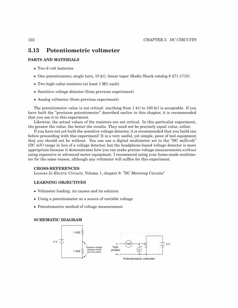
122 CHAPTER 3. DC CIRCUITS
3.13 Potentiometric voltmeter
PARTS AND MATERIALS
• Two 6 volt batteries
• One potentiometer, single turn, 10 kΩ, linear taper (Radio Shack catalog # 271-1715)
• Two high-value resistors (at least 1 MΩ each)
• Sensitive voltage detector (from previous experiment)
• Analog voltmeter (from previous experiment)
The potentiometer value is not critical: anything from 1 kΩ to 100 kΩ is acceptable. If youhave built the ”precision potentiometer” described earlier in this chapter, it is recommendedthat you use it in this experiment.
Likewise, the actual values of the resistors are not critical. In this particular experiment,the greater the value, the better the results. They need not be precisely equal value, either.
If you have not yet built the sensitive voltage detector, it is recommended that you build onebefore proceeding with this experiment! It is a very useful, yet simple, piece of test equipmentthat you should not be without. You can use a digital multimeter set to the ”DC millivolt”(DC mV) range in lieu of a voltage detector, but the headphone-based voltage detector is moreappropriate because it demonstrates how you can make precise voltage measurements without
using expensive or advanced meter equipment. I recommend using your home-made multime-ter for the same reason, although any voltmeter will suffice for this experiment.
CROSS-REFERENCES
Lessons In Electric Circuits, Volume 1, chapter 8: ”DC Metering Circuits”
LEARNING OBJECTIVES
• Voltmeter loading: its causes and its solution
• Using a potentiometer as a source of variable voltage
• Potentiometric method of voltage measurement
SCHEMATIC DIAGRAM
1 MΩ
1 MΩ
6 V
measure voltagebetween thesetwo test points
6 V+
V-
null
Potentiometric voltmeter
Testprobes

3.13. POTENTIOMETRIC VOLTMETER 123
ILLUSTRATION
+-
+-
- +
plug
headphones
Sensitivity
Test circuit
Potentiometric voltmeter circuit
Test probes
INSTRUCTIONS
Build the two-resistor voltage divider circuit shown on the left of the schematic diagramand of the illustration. If the two high-value resistors are of equal value, the battery’s voltageshould be split in half, with approximately 3 volts dropped across each resistor.
Measure the battery voltage directly with a voltmeter, then measure each resistor’s voltagedrop. Do you notice anything unusual about the voltmeter’s readings? Normally, series voltagedrops add to equal the total applied voltage, but in this case you will notice a serious discrep-ancy. Is Kirchhoff ’s Voltage Law untrue? Is this an exception to one of the most fundamentallaws of electric circuits? No! What is happening is this: when you connect a voltmeter acrosseither resistor, the voltmeter itself alters the circuit so that the voltage is not the same as withno meter connected.
I like to use the analogy of an air pressure gauge used to check the pressure of a pneumatictire. When a gauge is connected to the tire’s fill valve, it releases some air out of the tire.This affects the pressure in the tire, and so the gauge reads a slightly lower pressure thanwhat was in the tire before the gauge was connected. In other words, the act of measuringtire pressure alters the tire’s pressure. Hopefully, though, there is so little air released fromthe tire during the act of measurement that the reduction in pressure is negligible. Voltmeterssimilarly impact the voltage they measure, by bypassing some current around the componentwhose voltage drop is being measured. This affects the voltage drop, but the effect is so slightthat you usually don’t notice it.
In this circuit, though, the effect is very pronounced. Why is this? Try replacing the twohigh-value resistors with two of 100 kΩ value each and repeat the experiment. Replace thoseresistors with two 10 KΩ units and repeat. What do you notice about the voltage readings with

124 CHAPTER 3. DC CIRCUITS
lower-value resistors? What does this tell you about voltmeter ”impact” on a circuit in relationto that circuit’s resistance? Replace any low-value resistors with the original, high-value (>=1 MΩ) resistors before proceeding.
Try measuring voltage across the two high-value resistors – one at a time – with a digitalvoltmeter instead of an analog voltmeter. What do you notice about the digital meter’s readingsversus the analog meter’s? Digital voltmeters typically have greater internal (probe-to-probe)resistance, meaning they draw less current than a comparable analog voltmeter when mea-suring the same voltage source. An ideal voltmeter would draw zero current from the circuitunder test, and thus suffer no voltage ”impact” problems.
If you happen to have two voltmeters, try this: connect one voltmeter across one resistor,and the other voltmeter across the other resistor. The voltage readings you get will add upto the total voltage this time, no matter what the resistor values are, even though they’redifferent from the readings obtained from a single meter used twice. Unfortunately, though, itis unlikely that the voltage readings obtained this way are equal to the true voltage drops withno meters connected, and so it is not a practical solution to the problem.
Is there any way to make a ”perfect” voltmeter: one that has infinite resistance and drawsno current from the circuit under test? Modern laboratory voltmeters approach this goal byusing semiconductor ”amplifier” circuits, but this method is too technologically advanced forthe student or hobbyist to duplicate. A much simpler and much older technique is called thepotentiometric or null-balance method. This involves using an adjustable voltage source to”balance” the measured voltage. When the two voltages are equal, as indicated by a verysensitive null detector, the adjustable voltage source is measured with an ordinary voltmeter.Because the two voltage sources are equal to each other, measuring the adjustable source isthe same as measuring across the test circuit, except that there is no ”impact” error becausethe adjustable source provides any current needed by the voltmeter. Consequently, the circuitunder test remains unaffected, allowing measurement of its true voltage drop.
Examine the following schematic to see how the potentiometric voltmeter method is imple-mented:
1 MΩ
1 MΩ
6 V6 V
+V
-
null
Potentiometric voltmeterTest circuit
+
-
The circle symbol with the word ”null” written inside represents the null detector. This canbe any arbitrarily sensitive meter movement or voltage indicator. Its sole purpose in this circuitis to indicate when there is zero voltage: when the adjustable voltage source (potentiometer)is precisely equal to the voltage drop in the circuit under test. The more sensitive this nulldetector is, the more precisely the adjustable source may be adjusted to equal the voltage

3.13. POTENTIOMETRIC VOLTMETER 125
under test, and the more precisely that test voltage may be measured.
Build this circuit as shown in the illustration and test its operation measuring the voltagedrop across one of the high-value resistors in the test circuit. It may be easier to use a regularmultimeter as a null detector at first, until you become familiar with the process of adjust-ing the potentiometer for a ”null” indication, then reading the voltmeter connected across thepotentiometer.
If you are using the headphone-based voltage detector as your null meter, you will needto intermittently make and break contact with the circuit under test and listen for ”clicking”sounds. Do this by firmly securing one of the test probes to the test circuit and momentarilytouching the other test probe to the other point in the test circuit again and again, listeningfor sounds in the headphones indicating a difference of voltage between the test circuit andthe potentiometer. Adjust the potentiometer until no clicking sounds can be heard from theheadphones. This indicates a ”null” or ”balanced” condition, and you may read the voltmeterindication to see how much voltage is dropped across the test circuit resistor. Unfortunately,the headphone-based null detector provides no indication of whether the potentiometer voltageis greater than, or less than the test circuit voltage, so you will have to listen for decreasing
”click” intensity while turning the potentiometer to determine if you need to adjust the voltagehigher or lower.
You may find that a single-turn (”3/4 turn”) potentiometer is too coarse of an adjustmentdevice to accurately ”null” the measurement circuit. A multi-turn potentiometer may be usedinstead of the single-turn unit for greater adjustment precision, or the ”precision potentiome-ter” circuit described in an earlier experiment may be used.
Prior to the advent of amplified voltmeter technology, the potentiometric method was theonlymethod for making highly accurate voltage measurements. Even now, electrical standardslaboratories make use of this technique along with the latest meter technology to minimize me-ter ”impact” errors and maximize measurement accuracy. Although the potentiometric methodrequires more skill to use than simply connecting a modern digital voltmeter across a compo-nent, and is considered obsolete for all but the most precise measurement applications, it isstill a valuable learning process for the new student of electronics, and a useful technique forthe hobbyist who may lack expensive instrumentation in their home laboratory.
COMPUTER SIMULATION
Schematic with SPICE node numbers:

126 CHAPTER 3. DC CIRCUITS
1 MΩ
1 MΩ+
V-
null+
-
V1
1
0 00 0
1
2 2 3 3
V2
R1
R2
Netlist (make a text file containing the following text, verbatim):Potentiometric voltmeterv1 1 0 dc 6v2 3 0r1 1 2 1megr2 2 0 1megrnull 2 3 10krmeter 3 0 50k.dc v2 0 6 0.5.print dc v(2,0) v(2,3) v(3,0).end
This SPICE simulation shows the actual voltage across R2 of the test circuit, the null de-tector’s voltage, and the voltage across the adjustable voltage source, as that source is adjustedfrom 0 volts to 6 volts in 0.5 volt steps. In the output of this simulation, you will notice thatthe voltage across R2 is impacted significantly when the measurement circuit is unbalanced,returning to its true voltage only when there is practically zero voltage across the null detec-tor. At that point, of course, the adjustable voltage source is at a value of 3.000 volts: preciselyequal to the (unaffected) test circuit voltage drop.
What is the lesson to be learned from this simulation? That a potentiometric voltmeteravoids impacting the test circuit only when it is in a condition of perfect balance (”null”) withthe test circuit!

3.14. 4-WIRE RESISTANCE MEASUREMENT 127
3.14 4-wire resistance measurement
PARTS AND MATERIALS
• 6-volt battery
• Electromagnet made from experiment in previous chapter, or a large spool of wire
It would be ideal in this experiment to have two meters: one voltmeter and one ammeter.For experimenters on a budget, this may not be possible. Whatever ammeter is used should becapable measuring at least a few amps of current. A 6-volt ”lantern” battery essentially short-circuited by a long piece of wire may produce currents of this magnitude, and your ammeterneeds to be capable of measuring it without blowing a fuse or sustaining other damage. Makesure the highest current range on the meter is at least 5 amps!
CROSS-REFERENCES
Lessons In Electric Circuits, Volume 1, chapter 8: ”DC Metering Circuits”
LEARNING OBJECTIVES
• Operating principle of Kelvin (4-wire) resistance measurement
• How to measure low resistances with common test equipment
SCHEMATIC DIAGRAM
A+
V-
Runknown
+ -
ILLUSTRATION

128 CHAPTER 3. DC CIRCUITS
+-
COMA
V
V A
AOFF
COMA
V
V A
AOFF
Runknown
INSTRUCTIONS
Although this experiment is best performed with two meters, and indeed is shown as suchin the schematic diagram and illustration, one multimeter is sufficient.
Most ohmmeters operate on the principle of applying a small voltage across an unknownresistance (Runknown) and inferring resistance from the amount of current drawn by it. Exceptin special cases such as the megger, both the voltage and current quantities employed by themeter are quite small.
This presents a problem for measurement of low resistances, as a low resistance specimenmay be of much smaller resistance value than the meter circuitry itself. Imagine trying tomeasure the diameter of a cotton thread with a yardstick, or measuring the weight of a coinwith a scale built for weighing freight trucks, and you will appreciate the problem at hand.
One of the many sources of error in measuring small resistances with an ordinary ohmme-ter is the resistance of the ohmmeter’s own test leads. Being part of the measurement circuit,the test leads may contain more resistance than the resistance of the test specimen, incurringsignificant measurement error by their presence:
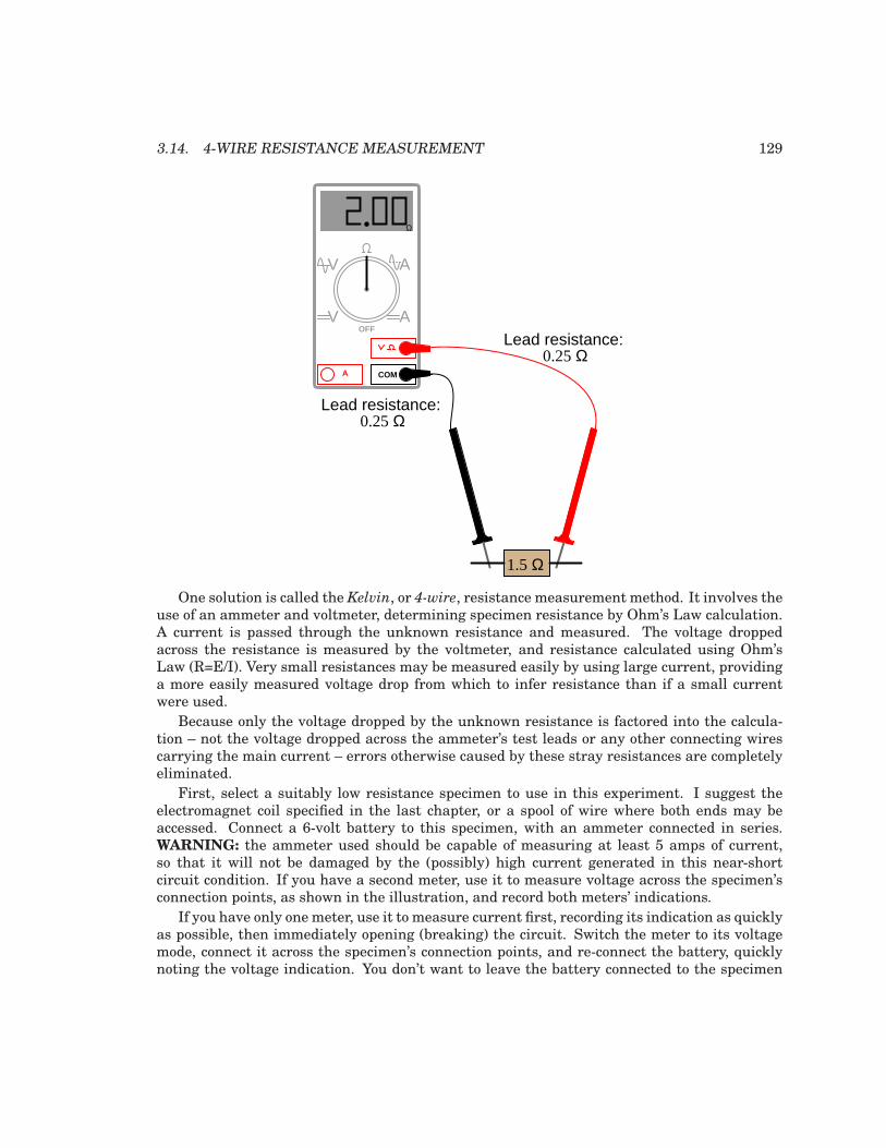
3.14. 4-WIRE RESISTANCE MEASUREMENT 129
COMA
V
V A
AOFF
1.5 Ω
0.25 Ω
0.25 Ω
Lead resistance:
Lead resistance:
Ω
One solution is called the Kelvin, or 4-wire, resistance measurement method. It involves theuse of an ammeter and voltmeter, determining specimen resistance by Ohm’s Law calculation.A current is passed through the unknown resistance and measured. The voltage droppedacross the resistance is measured by the voltmeter, and resistance calculated using Ohm’sLaw (R=E/I). Very small resistances may be measured easily by using large current, providinga more easily measured voltage drop from which to infer resistance than if a small currentwere used.
Because only the voltage dropped by the unknown resistance is factored into the calcula-tion – not the voltage dropped across the ammeter’s test leads or any other connecting wirescarrying the main current – errors otherwise caused by these stray resistances are completelyeliminated.
First, select a suitably low resistance specimen to use in this experiment. I suggest theelectromagnet coil specified in the last chapter, or a spool of wire where both ends may beaccessed. Connect a 6-volt battery to this specimen, with an ammeter connected in series.WARNING: the ammeter used should be capable of measuring at least 5 amps of current,so that it will not be damaged by the (possibly) high current generated in this near-shortcircuit condition. If you have a second meter, use it to measure voltage across the specimen’sconnection points, as shown in the illustration, and record both meters’ indications.
If you have only one meter, use it to measure current first, recording its indication as quicklyas possible, then immediately opening (breaking) the circuit. Switch the meter to its voltagemode, connect it across the specimen’s connection points, and re-connect the battery, quicklynoting the voltage indication. You don’t want to leave the battery connected to the specimen
130 CHAPTER 3. DC CIRCUITS
for any longer than necessary for obtaining meter measurements, as it will begin to rapidlydischarge due to the high circuit current, thus compromising measurement accuracy when themeter is re-configured and the circuit closed once more for the next measurement. When twometers are used, this is not as significant an issue, because the current and voltage indicationsmay be recorded simultaneously.
Take the voltage measurement and divide it by the current measurement. The quotientwill be equal to the specimen’s resistance in ohms.

3.15. A VERY SIMPLE COMPUTER 131
3.15 A very simple computer
PARTS AND MATERIALS
• Three batteries, each one with a different voltage
• Three equal-value resistors, between 10 kΩ and 47 kΩ each
When selecting resistors, measure each one with an ohmmeter and choose three that arethe closest in value to each other. Precision is very important for this experiment!
CROSS-REFERENCES
Lessons In Electric Circuits, Volume 1, chapter 10: ”DC Network Analysis”
LEARNING OBJECTIVES
• How a resistor network can function as a voltage signal averager
• Application of Millman’s Theorem
SCHEMATIC DIAGRAM
R1 R2 R3
+V
-
ILLUSTRATION

132 CHAPTER 3. DC CIRCUITS
+-
+ -
COMA
V
V A
AOFF

3.15. A VERY SIMPLE COMPUTER 133
+-
+ -
COMA
V
V A
AOFF
INSTRUCTIONS
This deceptively crude circuit performs the function of mathematically averaging three volt-age signals together, and so fulfills a specialized computational role. In other words, it is acomputer that can only do one mathematical operation: averaging three quantities together.
Build this circuit as shown and measure all battery voltages with a voltmeter. Write thesevoltage figures on paper and average them together (E1 + E2 + E3, divided by three). Whenyou measure each battery voltage, keep the black test probe connected to the ”ground” point(the side of the battery directly joined to the other batteries by jumper wires), and touch thered probe to the other battery terminal. Polarity is important here! You will notice one bat-tery in the schematic diagram connected ”backward” to the other two, negative side ”up.” Thisbattery’s voltage should read as a negative quantity when measured by a properly connecteddigital meter, the other batteries measuring positive.
When the voltmeter is connected to the circuit at the point shown in the schematic andillustrations, it should register the algebraic average of the three batteries’ voltages. If the

134 CHAPTER 3. DC CIRCUITS
resistor values are chosen to match each other very closely, the ”output” voltage of this circuitshould match the calculated average very closely as well.
If one battery is disconnected, the output voltage will equal the average voltage of the re-maining batteries. If the jumper wires formerly connecting the removed battery to the averagercircuit are connected to each other, the circuit will average the two remaining voltages togetherwith 0 volts, producing a smaller output signal:
+-
+ -
COMA
V
V A
AOFF
The sheer simplicity of this circuit deters most people from calling it a ”computer,” but itundeniably performs the mathematical function of averaging. Not only does it perform thisfunction, but it performs it much faster than any modern digital computer can! Digital com-puters, such as personal computers (PCs) and pushbutton calculators, perform mathematicaloperations in a series of discrete steps. Analog computers perform calculations in continu-ous fashion, exploiting Ohm’s and Kirchhoff ’s Laws for an arithmetic purpose, the ”answer”computed as fast as voltage propagates through the circuit (ideally, at the speed of light!).
With the addition of circuits called amplifiers, voltage signals in analog computer networksmay be boosted and re-used in other networks to perform a wide variety of mathematical func-tions. Such analog computers excel at performing the calculus operations of numerical dif-ferentiation and integration, and as such may be used to simulate the behavior of complexmechanical, electrical, and even chemical systems. At one time, analog computers were the

3.15. A VERY SIMPLE COMPUTER 135
ultimate tool for engineering research, but since then have been largely supplanted by digitalcomputer technology. Digital computers enjoy the advantage of performing mathematical op-erations with much better precision than analog computers, albeit at much slower theoreticalspeeds.
COMPUTER SIMULATION
Schematic with SPICE node numbers:
R1 R2 R3
+V
-
0
1 2 3
4
0 0
4 4 4
0
V1 V2 V3
Netlist (make a text file containing the following text, verbatim):Voltage averagerv1 1 0v2 0 2 dc 9v3 3 0 dc 1.5r1 1 4 10kr2 2 4 10kr3 3 4 10k.dc v1 6 6 1.print dc v(4,0).end
With this SPICE netlist, we can force a digital computer to simulate and analog computer,which averages three numbers together. Obviously, we aren’t doing this for the practical taskof averaging numbers, but rather to learn more about circuits and more about computer simu-lation of circuits!

136 CHAPTER 3. DC CIRCUITS
3.16 Potato battery
PARTS AND MATERIALS
• One large potato
• One lemon (optional)
• Strip of zinc, or galvanized metal
• Piece of thick copper wire
The basic experiment is based on the use of a potato, but many fruits and vegetables workas potential batteries!
For the zinc electrode, a large galvanized nail works well. Nails with a thick, rough zinctexture are preferable to galvanized nails that are smooth.
CROSS-REFERENCES
Lessons In Electric Circuits, Volume 1, chapter 11: ”Batteries and Power Systems”
LEARNING OBJECTIVES
• The importance of chemical activity in battery operation
• How electrode surface area affects battery operation
ILLUSTRATION
Potato
Galvanizednail
Copperwire
COMA
V
V A
AOFF
INSTRUCTIONS

3.16. POTATO BATTERY 137
Push both the nail and the wire deep into the potato. Measure voltage output by the potatobattery with a voltmeter. Now, wasn’t that easy?
Seriously, though, experiment with different metals, electrode depths, and electrode spac-ings to obtain the greatest voltage possible from the potato. Try other vegetables or fruits andcompare voltage output with the same electrode metals.
It can be difficult to power a load with a single ”potato” battery, so don’t expect to light upan incandescent lamp or power a hobby motor or do anything like that. Even if the voltageoutput is adequate, a potato battery has a fairly high internal resistance which causes itsvoltage to ”sag” badly under even a light load. With multiple potato batteries connected inseries, parallel, or series-parallel arrangement, though, it is possible to obtain enough voltageand current capacity to power a small load.

138 CHAPTER 3. DC CIRCUITS
3.17 Capacitor charging and discharging
PARTS AND MATERIALS
• 6 volt battery
• Two large electrolytic capacitors, 1000 µF minimum (Radio Shack catalog # 272-1019,272-1032, or equivalent)
• Two 1 kΩ resistors
• One toggle switch, SPST (”Single-Pole, Single-Throw”)
Large-value capacitors are required for this experiment to produce time constants slowenough to track with a voltmeter and stopwatch. Be warned that most large capacitors are ofthe ”electrolytic” type, and they are polarity sensitive! One terminal of each capacitor shouldbe marked with a definite polarity sign. Usually capacitors of the size specified have a negative(-) marking or series of negative markings pointing toward the negative terminal. Very largecapacitors are often polarity-labeled by a positive (+) marking next to one terminal. Failure toheed proper polarity will almost surely result in capacitor failure, even with a source voltageas low as 6 volts. When electrolytic capacitors fail, they typically explode, spewing causticchemicals and emitting foul odors. Please, try to avoid this!
I recommend a household light switch for the ”SPST toggle switch” specified in the partslist.
CROSS-REFERENCES
Lessons In Electric Circuits, Volume 1, chapter 13: ”Capacitors”
Lessons In Electric Circuits, Volume 1, chapter 16: ”RC and L/R Time Constants”
LEARNING OBJECTIVES
• Capacitor charging action
• Capacitor discharging action
• Time constant calculation
• Series and parallel capacitance
SCHEMATIC DIAGRAM

3.17. CAPACITOR CHARGING AND DISCHARGING 139
+V
-
Charging circuit
+V
-
Discharging circuit
ILLUSTRATION
--
+-
Charging circuit

140 CHAPTER 3. DC CIRCUITS
--
+-
Discharging circuit
INSTRUCTIONS
Build the ”charging” circuit and measure voltage across the capacitor when the switch isclosed. Notice how it increases slowly over time, rather than suddenly as would be the casewith a resistor. You can ”reset” the capacitor back to a voltage of zero by shorting across itsterminals with a piece of wire.
The ”time constant” (τ ) of a resistor capacitor circuit is calculated by taking the circuitresistance and multiplying it by the circuit capacitance. For a 1 kΩ resistor and a 1000 µFcapacitor, the time constant should be 1 second. This is the amount of time it takes for thecapacitor voltage to increase approximately 63.2% from its present value to its final value: thevoltage of the battery.
It is educational to plot the voltage of a charging capacitor over time on a sheet of graphpaper, to see how the inverse exponential curve develops. In order to plot the action of thiscircuit, though, we must find a way of slowing it down. A one-second time constant doesn’tprovide much time to take voltmeter readings!
We can increase this circuit’s time constant two different ways: changing the total circuitresistance, and/or changing the total circuit capacitance. Given a pair of identical resistors anda pair of identical capacitors, experiment with various series and parallel combinations to ob-tain the slowest charging action. You should already know by now how multiple resistors needto be connected to form a greater total resistance, but what about capacitors? This circuit willdemonstrate to you how capacitance changes with series and parallel capacitor connections.Just be sure that you insert the capacitor(s) in the proper direction: with the ends labelednegative (-) electrically ”closest” to the battery’s negative terminal!
The discharging circuit provides the same kind of changing capacitor voltage, except thistime the voltage jumps to full battery voltage when the switch closes and slowly falls whenthe switch is opened. Experiment once again with different combinations of resistors andcapacitors, making sure as always that the capacitor’s polarity is correct.
COMPUTER SIMULATION
Schematic with SPICE node numbers:
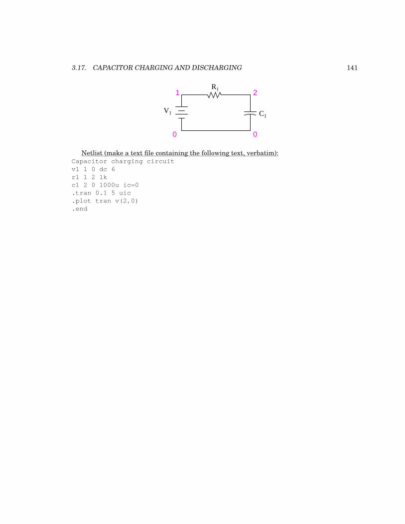
3.17. CAPACITOR CHARGING AND DISCHARGING 141
V1
R1
C1
1
0 0
2
Netlist (make a text file containing the following text, verbatim):Capacitor charging circuitv1 1 0 dc 6r1 1 2 1kc1 2 0 1000u ic=0.tran 0.1 5 uic.plot tran v(2,0).end

142 CHAPTER 3. DC CIRCUITS
3.18 Rate-of-change indicator
PARTS AND MATERIALS
• Two 6 volt batteries
• Capacitor, 0.1 µF (Radio Shack catalog # 272-135)
• 1 MΩ resistor
• Potentiometer, single turn, 5 kΩ, linear taper (Radio Shack catalog # 271-1714)
The potentiometer value is not especially critical, although lower-resistance units will, intheory, work better for this experiment than high-resistance units. I’ve used a 10 kΩ poten-tiometer for this circuit with excellent results.
CROSS-REFERENCES
Lessons In Electric Circuits, Volume 1, chapter 13: ”Capacitors”
LEARNING OBJECTIVES
• How to build a differentiator circuit
• Obtain an empirical understanding of the derivative calculus function
SCHEMATIC DIAGRAM
1 MΩ
0.1 µF
5 kΩ6 V
6 V
+V
-
ILLUSTRATION

3.18. RATE-OF-CHANGE INDICATOR 143
+-
+-
COMA
V
V A
AOFF
INSTRUCTIONS
Measure voltage between the potentiometer’s wiper terminal and the ”ground” point shownin the schematic diagram (the negative terminal of the lower 6-volt battery). This is the inputvoltage for the circuit, and you can see how it smoothly varies between zero and 12 volts as thepotentiometer control is turned full-range. Since the potentiometer is used here as a voltagedivider, this behavior should be unsurprising to you.
Now, measure voltage across the 1 MΩ resistor while moving the potentiometer control. Adigital voltmeter is highly recommended, and I advise setting it to a very sensitive (millivolt)range to obtain the strongest indications. What does the voltmeter indicate while the poten-tiometer is not being moved? Turn the potentiometer slowly clockwise and note the voltmeter’sindication. Turn the potentiometer slowly counter-clockwise and note the voltmeter’s indica-tion. What difference do you see between the two different directions of potentiometer controlmotion?
Try moving the potentiometer in such a way that the voltmeter gives a steady, small in-dication. What kind of potentiometer motion provides the steadiest voltage across the 1 MΩ
resistor?In calculus, a function representing the rate of change of one variable as compared to an-
other is called the derivative. This simple circuit illustrates the concept of the derivative byproducing an output voltage proportional to the input voltage’s rate of change over time. Be-

144 CHAPTER 3. DC CIRCUITS
cause this circuit performs the calculus function of differentiation with respect to time (out-putting the time-derivative of an incoming signal), it is called a differentiator circuit.
Like the averager circuit shown earlier in this chapter, the differentiator circuit is a kind ofanalog computer. Differentiation is a far more complex mathematical function than averaging,especially when implemented in a digital computer, so this circuit is an excellent demonstrationof the elegance of analog circuitry in performing mathematical computations.
More accurate differentiator circuits may be built by combining resistor-capacitor networkswith electronic amplifier circuits. For more detail on computational circuitry, go to the ”AnalogIntegrated Circuits” chapter in this Experiments volume.

Chapter 4
AC CIRCUITS
Contents
4.1 Introduction . . . . . . . . . . . . . . . . . . . . . . . . . . . . . . . . . . . . . . 145
4.2 Transformer – power supply . . . . . . . . . . . . . . . . . . . . . . . . . . . . 147
4.3 Build a transformer . . . . . . . . . . . . . . . . . . . . . . . . . . . . . . . . . 151
4.4 Variable inductor . . . . . . . . . . . . . . . . . . . . . . . . . . . . . . . . . . . 153
4.5 Sensitive audio detector . . . . . . . . . . . . . . . . . . . . . . . . . . . . . . 155
4.6 Sensing AC magnetic fields . . . . . . . . . . . . . . . . . . . . . . . . . . . . . 160
4.7 Sensing AC electric fields . . . . . . . . . . . . . . . . . . . . . . . . . . . . . . 162
4.8 Automotive alternator . . . . . . . . . . . . . . . . . . . . . . . . . . . . . . . . 164
4.9 Induction motor . . . . . . . . . . . . . . . . . . . . . . . . . . . . . . . . . . . . 170
4.10 Induction motor, large . . . . . . . . . . . . . . . . . . . . . . . . . . . . . . . 174
4.11 Phase shift . . . . . . . . . . . . . . . . . . . . . . . . . . . . . . . . . . . . . . . 177
4.12 Sound cancellation . . . . . . . . . . . . . . . . . . . . . . . . . . . . . . . . . . 180
4.13 Musical keyboard as a signal generator . . . . . . . . . . . . . . . . . . . . . 183
4.14 PC Oscilloscope . . . . . . . . . . . . . . . . . . . . . . . . . . . . . . . . . . . . 186
4.15 Waveform analysis . . . . . . . . . . . . . . . . . . . . . . . . . . . . . . . . . . 189
4.16 Inductor-capacitor ”tank” circuit . . . . . . . . . . . . . . . . . . . . . . . . . 191
4.17 Signal coupling . . . . . . . . . . . . . . . . . . . . . . . . . . . . . . . . . . . . 194
4.1 Introduction
”AC” stands for Alternating Current, which can refer to either voltage or current that alter-nates in polarity or direction, respectively. These experiments are designed to introduce you toseveral important concepts specific to AC.
A convenient source of AC voltage is household wall-socket power, which presents signifi-cant shock hazard. In order to minimize this hazard while taking advantage of the convenience
145

146 CHAPTER 4. AC CIRCUITS
of this source of AC, a small power supply will be the first project, consisting of a transformer
that steps the hazardous voltage (110 to 120 volts AC, RMS) down to 12 volts or less. The titleof ”power supply” is somewhat misleading. This device does not really act as a source or supplyof power, but rather as a power converter, to reduce the hazardous voltage of wall-socket powerto a much safer level.
4.2. TRANSFORMER – POWER SUPPLY 147
4.2 Transformer – power supply
PARTS AND MATERIALS
• Power transformer, 120VAC step-down to 12VAC, with center-tapped secondary winding(Radio Shack catalog # 273-1365, 273-1352, or 273-1511).
• Terminal strip with at least three terminals.
• Household wall-socket power plug and cord.
• Line cord switch.
• Box (optional).
• Fuse and fuse holder (optional).
Power transformers may be obtained from old radios, which can usually be obtained froma thrift store for a few dollars (or less!). The radio would also provide the power cord andplug necessary for this project. Line cord switches may be obtained from a hardware store. Ifyou want to be absolutely sure what kind of transformer you’re getting, though, you shouldpurchase one from an electronics supply store.
If you decide to equip your power supply with a fuse, be sure to get a slow-acting, or slow-
blow fuse. Transformers may draw high ”surge” currents when initially connected to an ACsource, and these transient currents will blow a fast-acting fuse. Determine the proper cur-rent rating of the fuse by dividing the transformer’s ”VA” rating by 120 volts: in other words,calculate the full allowable primary winding current and size the fuse accordingly.
CROSS-REFERENCES
Lessons In Electric Circuits, Volume 2, chapter 1: ”Basic AC Theory”
Lessons In Electric Circuits, Volume 2, chapter 9: ”Transformers”
LEARNING OBJECTIVES
• Transformer voltage step-down behavior.
• Purpose of tapped windings.
• Safe wiring techniques for power cords.
SCHEMATIC DIAGRAM

148 CHAPTER 4. AC CIRCUITS
Fuse
(optional)
Switch
Transformer
Plug
Box (optional)
ILLUSTRATION
120 volts
12 / 6 volts CT
2-conductor"zip" cord "zip" cord split into
separate wires
wires soldered and tapedwith electrical tape
line switch
wires soldered and tapedwith electrical tape
Transformer
plug
Terminalstrip
INSTRUCTIONS
Warning! This project involves the use of dangerous voltages. You must make sure all high-voltage (120 volt household power) conductors are safely insulated from accidental contact. Nobare wires should be seen anywhere on the ”primary” side of the transformer circuit. Be sureto solder all wire connections so that they’re secure, and use real electrical tape (not duct tape,scotch tape, packing tape, or any other kind!) to insulate your soldered connections.
If you wish to enclose the transformer inside of a box, you may use an electrical ”junction”box, obtained from a hardware store or electrical supply house. If the enclosure used is metalrather than plastic, a three-prong plug should be used, with the ”ground” prong (the longestone on the plug) connected directly to the metal case for maximum safety.
Before plugging the plug into a wall socket, do a safety check with an ohmmeter. With theline switch in the ”on” position, measure resistance between either plug prong and the trans-former case. There should be infinite (maximum) resistance. If the meter registers continuity(some resistance value less than infinity), then you have a ”short” between one of the powerconductors and the case, which is dangerous!

4.2. TRANSFORMER – POWER SUPPLY 149
Next, check the transformer windings themselves for continuity. With the line switch in the”on” position, there should be a small amount of resistance between the two plug prongs. Whenthe switch is turned ”off,” the resistance indication should increase to infinity (open circuit – nocontinuity). Measure resistance between pairs of wires on the secondary side. These secondarywindings should register much lower resistances than the primary. Why is this?
Plug the cord into a wall socket and turn the switch on. You should be able to measure ACvoltage at the secondary side of the transformer, between pairs of terminals. Between two ofthese terminals, you should measure about 12 volts. Between either of these two terminalsand the third terminal, you should measure half that. This third wire is the ”center-tap” wireof the secondary winding.
It would be advisable to keep this project assembled for use in powering other experimentsshown in this book. From here on, I will designate this ”low-voltage AC power supply” usingthis illustration:
Low-voltage AC power supply
6 612
COMPUTER SIMULATION
Schematic with SPICE node numbers:
120 V
1
0 0
3
4
5
L1
L2
L3
Rbogus1
Rbogus2
1 mΩ
1 TΩ
2
Rload1
Rload2
Netlist (make a text file containing the following text, verbatim):transformer with center-tap secondaryv1 1 0 ac 120 sinrbogus1 1 2 1e-3l1 2 0 10l2 5 4 0.025l3 4 3 0.025k1 l1 l2 0.999k2 l2 l3 0.999

150 CHAPTER 4. AC CIRCUITS
k3 l1 l3 0.999rbogus2 3 0 1e12rload1 5 4 1krload2 4 3 1k
* Sets up AC analysis at 60 Hz:.ac lin 1 60 60
* Prints primary voltage between nodes 2 and 0:.print ac v(2,0)
* Prints (top) secondary voltage between nodes 5 and 4:.print ac v(5,4)
* Prints (bottom) secondary voltage between nodes 4 and 3:.print ac v(4,3)
* Prints (total) secondary voltage between nodes 5 and 3:.print ac v(5,3).end

4.3. BUILD A TRANSFORMER 151
4.3 Build a transformer
PARTS AND MATERIALS
• Steel flatbar, 4 pieces
• Miscellaneous bolts, nuts, washers
• 28 gauge ”magnet” wire
• Low-voltage AC power supply
”Magnet wire” is small-gauge wire insulated with a thin enamel coating. It is intended tobe used to make electromagnets, because many ”turns” of wire may be wrapped in a relativelysmall-diameter coil. Any gauge of wire will work, but 28 gauge is recommended so as to makea coil with as many turns as possible in a small diameter.
CROSS-REFERENCES
Lessons In Electric Circuits, Volume 2, chapter 9: ”Transformers”
LEARNING OBJECTIVES
• Effects of electromagnetism.
• Effects of electromagnetic induction.
• Effects of magnetic coupling on voltage regulation.
• Effects of winding turns on ”step” ratio.
SCHEMATIC DIAGRAM
Transformer
ILLUSTRATION

152 CHAPTER 4. AC CIRCUITS
wire coilwire coil
bolt
steel "flatbar"
INSTRUCTIONS
Wrap two, equal-length bars of steel with a thin layer of electrically-insulating tape. Wrapseveral hundred turns of magnet wire around these two bars. You may make these windingswith an equal or unequal number of turns, depending on whether or not you want the trans-former to be able to ”step” voltage up or down. I recommend equal turns to begin with, thenexperiment later with coils of unequal turn count.
Join those bars together in a rectangle with two other, shorter, bars of steel. Use bolts tosecure the bars together (it is recommended that you drill bolt holes through the bars before
you wrap wire around them).Check for shorted windings (ohmmeter reading between wire ends and steel bar) after
you’re finished wrapping the windings. There should be no continuity (infinite resistance)between the winding and the steel bar. Check for continuity between winding ends to ensurethat the wire isn’t broken open somewhere within the coil. If either resistance measurementsindicate a problem, the winding must be re-made.
Power your transformer with the low-voltage output of the ”power supply” described at thebeginning of this chapter. Do not power your transformer directly from wall-socket voltage(120 volts), as your home-made windings really aren’t rated for any significant voltage!
Measure the output voltage (secondary winding) of your transformer with an AC voltmeter.Connect a load of some kind (light bulbs are good!) to the secondary winding and re-measurevoltage. Note the degree of voltage ”sag” at the secondary winding as load current is increased.
Loosen or remove the connecting bolts from one of the short bar pieces, thus increasingthe reluctance (analogous to resistance) of the magnetic ”circuit” coupling the two windingstogether. Note the effect on output voltage and voltage ”sag” under load.
If you’ve made your transformer with unequal-turn windings. try it in step-up versus step-down mode, powering different AC loads.

4.4. VARIABLE INDUCTOR 153
4.4 Variable inductor
PARTS AND MATERIALS
• Paper tube, from a toilet-paper roll
• Bar of iron or steel, large enough to almost fill diameter of paper tube
• 28 gauge ”magnet” wire
• Low-voltage AC power supply
• Incandescent lamp, rated for power supply voltage
CROSS-REFERENCES
Lessons In Electric Circuits, Volume 1, chapter 14: ”Magnetism and Electromagnetism”
Lessons In Electric Circuits, Volume 1, chapter 15: ”Inductors”
Lessons In Electric Circuits, Volume 2, chapter 3: ”Reactance and Impedance – Inductive”
LEARNING OBJECTIVES
• Effects of magnetic permeability on inductance.
• How inductive reactance can control current in an AC circuit.
SCHEMATIC DIAGRAM
Variable inductor
Lamp
ILLUSTRATION

154 CHAPTER 4. AC CIRCUITS
Steelbar
Papertube
wire coil
Low-voltage AC power supply
6 612
INSTRUCTIONS
Wrap hundreds of turns of magnet wire around the paper tube. Connect this home-madeinductor in series with an AC power supply and lamp to form a circuit. When the tube is empty,the lamp should glow brightly. When the steel bar is inserted in the tube, the lamp dims fromincreased inductance (L) and consequently increased inductive reactance (XL).
Try using bars of different materials, such as copper and stainless steel, if available. Notall metals have the same effect, due to differences in magnetic permeability.

4.5. SENSITIVE AUDIO DETECTOR 155
4.5 Sensitive audio detector
PARTS AND MATERIALS
• High-quality ”closed-cup” audio headphones
• Headphone jack: female receptacle for headphone plug (Radio Shack catalog # 274-312)
• Small step-down power transformer (Radio Shack catalog # 273-1365 or equivalent, usingthe 6-volt secondary winding tap)
• Two 1N4001 rectifying diodes (Radio Shack catalog # 276-1101)
• 1 kΩ resistor
• 100 kΩ potentiometer (Radio Shack catalog # 271-092)
• Two ”banana” jack style binding posts, or other terminal hardware, for connection topotentiometer circuit (Radio Shack catalog # 274-662 or equivalent)
• Plastic or metal mounting box
Regarding the headphones, the higher the ”sensitivity” rating in decibels (dB), the better,but listening is believing: if you’re serious about building a detector with maximum sensitivityfor small electrical signals, you should try a few different headphone models at a high-qualityaudio store and ”listen” for which ones produce an audible sound for the lowest volume settingon a radio or CD player. Beware, as you could spend hundreds of dollars on a pair of head-phones to get the absolute best sensitivity! Take heart, though: I’ve used an old pair of RadioShack ”Realistic” brand headphones with perfectly adequate results, so you don’t need to buythe best.
Normally, the transformer used in this type of application (audio speaker impedance match-ing) is called an ”audio transformer,” with its primary and secondary windings represented byimpedance values (1000 Ω : 8 Ω) instead of voltages. An audio transformer will work, but I’vefound small step-down power transformers of 120/6 volt ratio to be perfectly adequate for thetask, cheaper (especially when taken from an old thrift-store alarm clock radio), and far morerugged.
The tolerance (precision) rating for the 1 kΩ resistor is irrelevant. The 100 kΩ potentiome-ter is a recommended option for incorporation into this project, as it gives the user controlover the loudness for any given signal. Even though an audio-taper potentiometer would beappropriate for this application, it is not necessary. A linear-taper potentiometer works quitewell.
CROSS-REFERENCES
Lessons In Electric Circuits, Volume 1, chapter 8: ”DC Metering Circuits”Lessons In Electric Circuits, Volume 2, chapter 9: ”Transformers”Lessons In Electric Circuits, Volume 2, chapter 12: ”AC Metering Circuits”
LEARNING OBJECTIVES

156 CHAPTER 4. AC CIRCUITS
• Soldering practice
• Use of a transformer for impedance matching
• Detection of extremely small electrical signals
• Using diodes to ”clip” voltage at some maximum level
SCHEMATIC DIAGRAM
plugjack
transformertest lead
test lead
diodes
headphones
1 kΩ
ILLUSTRATION
6 V120 V
diodes
transformer jackplug
headphones
resistor
Bindingposts
INSTRUCTIONS
This experiment is identical in construction to the ”Sensitive Voltage Detector” describedin the DC experiments chapter. If you’ve already built this detector, you may skip this experi-ment.
The headphones, most likely being stereo units (separate left and right speakers) will havea three-contact plug. You will be connecting to only two of those three contact points. If youonly have a ”mono” headphone set with a two-contact plug, just connect to those two contactpoints. You may either connect the two stereo speakers in series or in parallel. I’ve found theseries connection to work best, that is, to produce the most sound from a small signal:

4.5. SENSITIVE AUDIO DETECTOR 157
common right left common right left
Speakers in series Speakers in parallel
To transformer To transformer
Solder all wire connections well. This detector system is extremely sensitive, and any loosewire connections in the circuit will add unwanted noise to the sounds produced by the mea-sured voltage signal. The two diodes connected in parallel with the transformer’s primarywinding, along with the series-connected 1 kΩ resistor, work together to ”clip” the input volt-age to a maximum of about 0.7 volts. This does one thing and one thing only: limit the amountof sound the headphones can produce. The system will work without the diodes and resistor inplace, but there will be no limit to sound volume in the circuit, and the resulting sound causedby accidentally connecting the test leads across a substantial voltage source (like a battery)can be deafening!
Binding posts provide points of connection for a pair of test probes with banana-style plugs,once the detector components are mounted inside a box. You may use ordinary multimeterprobes, or make your own probes with alligator clips at the ends for secure connection to acircuit.
Detectors are intended to be used for balancing bridge measurement circuits, potentiomet-ric (null-balance) voltmeter circuits, and detect extremely low-amplitude AC (”alternating cur-rent”) signals in the audio frequency range. It is a valuable piece of test equipment, especiallyfor the low-budget experimenter without an oscilloscope. It is also valuable in that it allowsyou to use a different bodily sense in interpreting the behavior of a circuit.
For connection across any non-trivial source of voltage (1 volt and greater), the detector’sextremely high sensitivity should be attenuated. This may be accomplished by connecting avoltage divider to the ”front” of the circuit:
SCHEMATIC DIAGRAM
test lead
test lead
kΩ100
1 kΩ
ILLUSTRATION

158 CHAPTER 4. AC CIRCUITS
potentiometer
Adjust the 100 kΩ voltage divider potentiometer to about mid-range when initially sensinga voltage signal of unknown magnitude. If the sound is too loud, turn the potentiometer downand try again. If too soft, turn it up and try again. This detector even senses DC and radio-frequency signals (frequencies below and above the audio range, respectively), a ”click” beingheard whenever the test leads make or break contact with the source under test. With mycheap headphones, I’ve been able to detect currents of less than 1/10 of a microamp (¡ 0.1 µA)DC, and similarly low-magnitude RF signals up to 2 MHz.
A good demonstration of the detector’s sensitivity is to touch both test leads to the endof your tongue, with the sensitivity adjustment set to maximum. The voltage produced bymetal-to-electrolyte contact (called galvanic voltage) is very small, but enough to produce soft”clicking” sounds every time the leads make and break contact on the wet skin of your tongue.
Try unplugging the headphone plug from the jack (receptacle) and similarly touching it tothe end of your tongue. You should still hear soft clicking sounds, but they will be much smallerin amplitude. Headphone speakers are ”low impedance” devices: they require low voltage and”high” current to deliver substantial sound power. Impedance is a measure of opposition to anyand all forms of electric current, including alternating current (AC). Resistance, by compari-son, is a strictly measure of opposition to direct current (DC). Like resistance, impedance ismeasured in the unit of the Ohm (Ω), but it is symbolized in equations by the capital letter ”Z”rather than the capital letter ”R”. We use the term ”impedance” to describe the headphone’s op-position to current because it is primarily AC signals that headphones are normally subjectedto, not DC.
Most small signal sources have high internal impedances, some much higher than the nom-inal 8 Ω of the headphone speakers. This is a technical way of saying that they are incapable ofsupplying substantial amounts of current. As the Maximum Power Transfer Theorem predicts,maximum sound power will be delivered by the headphone speakers when their impedance is”matched” to the impedance of the voltage source. The transformer does this. The transformeralso helps aid the detection of small DC signals by producing inductive ”kickback” every timethe test lead circuit is broken, thus ”amplifying” the signal by magnetically storing up electricalenergy and suddenly releasing it to the headphone speakers.
As with the low-voltage AC power supply experiment, I recommend building this detectorin a permanent fashion (mounting all components inside of a box, and providing nice test leadwires) so it can be easily used in the future. Constructed as such, it might look something likethis:

4.5. SENSITIVE AUDIO DETECTOR 159
plug
headphones
Sensitivity
Test leads

160 CHAPTER 4. AC CIRCUITS
4.6 Sensing AC magnetic fields
PARTS AND MATERIALS
• Audio detector with headphones
• Electromagnet coil from relay or solenoid
What is needed for an electromagnet coil is a coil with many turns of wire, so as to producethe most voltage possible from induction with stray magnetic fields. The coil taken from an oldrelay or solenoid works well for this purpose.
CROSS-REFERENCES
Lessons In Electric Circuits, Volume 2, chapter 7: ”Mixed-Frequency AC Signals”
LEARNING OBJECTIVES
• Effects of electromagnetic induction.
• Electromagnetic shielding techniques.
SCHEMATIC DIAGRAM
kΩ100
sensingcoil
Audio detector circuit
1 kΩ
ILLUSTRATION
plug
headphones
Sensitivity
sensingcoil
Audiodetectorcircuit

4.6. SENSING AC MAGNETIC FIELDS 161
INSTRUCTIONS
Using the audio detector circuit explained earlier to detect AC voltage in the audio frequen-cies, a coil of wire may serve as sensor of AC magnetic fields. The voltages produced by the coilwill be quite small, so it is advisable to adjust the detector’s sensitivity control to ”maximum.”
There are many sources of AC magnetic fields to be found in the average home. Try, for in-stance, holding the coil close to a television screen or circuit-breaker box. The coil’s orientationis every bit as important as its proximity to the source, as you will soon discover on your own!If you want to listen to more interesting tones, try holding the coil close to the motherboardof an operating computer (be careful not to ”short” any connections together on the computer’scircuit board with any exposed metal parts on the sensing coil!), or to its hard drive while aread/write operation is taking place.
One very strong source of AC magnetic fields is the home-made transformer project de-scribed earlier. Try experimenting with various degrees of ”coupling” between the coils (thesteel bars tightly fastened together, versus loosely fastened, versus dismantled). Anothersource is the variable inductor and lamp circuit described in another section of this chapter.
Note that physical contact with a magnetic field source is unnecessary: magnetic fieldsextend through space quite easily. You may also want to try ”shielding” the coil from a strongsource using various materials. Try aluminum foil, paper, sheet steel, plastic, or whateverother materials you can think of. What materials work best? Why? What angles (orientations)of coil position minimize magnetic coupling (result in a minimum of detected signal)? Whatdoes this tell us regarding inductor positioning if inter-circuit interference from other inductorsis a bad thing?
Whether or not stray magnetic fields like these pose any health hazard to the human bodyis a hotly debated subject. One thing is clear: in today’s modern society, low-level magneticfields of all frequencies are easy to find!

162 CHAPTER 4. AC CIRCUITS
4.7 Sensing AC electric fields
PARTS AND MATERIALS
• Audio detector with headphones
CROSS-REFERENCES
Lessons In Electric Circuits, Volume 2, chapter 7: ”Mixed-Frequency AC Signals”
LEARNING OBJECTIVES
• Effects of electrostatic (capacitive) coupling.
• Electrostatic shielding techniques.
SCHEMATIC DIAGRAM
kΩ100
Audio detector circuit
sensingwire
1 kΩ
ILLUSTRATION
plug
headphones
Sensitivity
sensingAudiodetectorcircuitwire
connection towater pipe
4.7. SENSING AC ELECTRIC FIELDS 163
INSTRUCTIONS
”Ground” one lead of the detector to a metal object in contact with the earth (dirt). Mostany water pipe or faucet in a house will suffice. Take the other lead and hold it close to anelectrical appliance or lamp fixture. Do not try to make contact with the appliance or
with any conductors within! Any AC electric fields produced by the appliance will be heardin the headphones as a buzzing tone.
Try holding the wire in different positions next to a good, strong source of electric fields. Tryusing a piece of aluminum foil clipped to the wire’s end to maximize capacitance (and thereforeits ability to intercept an electric field). Try using different types of material to ”shield” thewire from an electric field source. What material(s) work best? How does this compare withthe AC magnetic field experiment?
As with magnetic fields, there is controversy whether or not stray electric fields like thesepose any health hazard to the human body.

164 CHAPTER 4. AC CIRCUITS
4.8 Automotive alternator
PARTS AND MATERIALS
• Automotive alternator (one required, but two recommended)
Old alternators may be obtained for low prices at automobile wrecking yards. Many yardshave alternators already removed from the automobile, for your convenience. I do not recom-mend paying full price for a new alternator, as used units cost far less money and function justas well for the purposes of this experiment.
I highly recommend using a Delco-Remy brand of alternator. This is the type used onGeneral Motors (GMC, Chevrolet, Cadillac, Buick, Oldsmobile) vehicles. One particular modelhas been produced by Delco-Remy since the early 1960’s with little design change. It is a very
common unit to locate in a wrecking yard, and very easy to work with.If you obtain two alternators, you may use one as a generator and the other as a motor. The
steps needed to prepare an alternator as a three-phase generator and as a three-phase motorare the same.
CROSS-REFERENCES
Lessons In Electric Circuits, Volume 1, chapter 14: ”Magnetism and Electromagnetism”Lessons In Electric Circuits, Volume 2, chapter 10: ”Polyphase AC Circuits”
LEARNING OBJECTIVES
• Effects of electromagnetism
• Effects of electromagnetic induction
• Construction of real electromagnetic machines
• Construction and application of three-phase windings
SCHEMATIC DIAGRAM
Typical alternator
shaft
"field"terminals
"battery"terminal
An automotive alternator is a three-phase generator with a built-in rectifier circuit consist-ing of six diodes. As the sheave (most people call it a ”pulley”) is rotated by a belt connected

4.8. AUTOMOTIVE ALTERNATOR 165
to the automobile engine’s crankshaft, a magnet is spun past a stationary set of three-phasewindings (called the stator), usually connected in a Y configuration. The spinning magnet isactually an electromagnet, not a permanent magnet. Alternators are designed this way so thatthe magnetic field strength can be controlled, in order that output voltage may be controlledindependently of rotor speed. This rotor magnet coil (called the field coil, or simply field) isenergized by battery power, so that it takes a small amount of electrical power input to thealternator to get it to generate a lot of output power.
Electrical power is conducted to the rotating field coil through a pair of copper ”slip rings”mounted concentrically on the shaft, contacted by stationary carbon ”brushes.” The brushesare held in firm contact with the slip rings by spring pressure.
Many modern alternators are equipped with built-in ”regulator” circuits that automaticallyswitch battery power on and off to the rotor coil to regulate output voltage. This circuit, ifpresent in the alternator you choose for the experiment, is unnecessary and will only impedeyour study if left in place. Feel free to ”surgically remove” it, just make sure you leave accessto the brush terminals so that you can power the field coil with the alternator fully assembled.
ILLUSTRATION
INSTRUCTIONS
First, consult an automotive repair manual on the specific details of your alternator. Thedocumentation provided in the book you’re reading now is as general as possible to accommo-date different brands of alternators. You may need more specific information, and a servicemanual is the best place to obtain it.
For this experiment, you’ll be connecting wires to the coils inside the alternator and ex-tending them outside the alternator case, for easy connection to test equipment and circuits.Unfortunately, the connection terminals provided by the manufacturer won’t suit our needshere, so you need to make your own connections.
Disassemble the unit and locate terminals for connecting to the two carbon brushes. Soldera pair of wires to these terminals (at least 20 gauge in size) and extend these wires throughvent holes in the alternator case, making sure they won’t get snagged on the spinning rotorwhen the alternator is re-assembled and used.
Locate the three-phase line connections coming from the stator windings and connect wiresto them as well, extending these wires outside the alternator case through some vent holes.Use the largest gauge wire that is convenient to work with for these wires, as they may becarrying substantial current. As with the field wires, route them in such a way that the rotorwill turn freely with the alternator reassembled. The stator winding line terminals are easy

166 CHAPTER 4. AC CIRCUITS
to locate: the three of them connect to three terminals on the diode assembly, usually with”ring-lug” terminals soldered to the ends of the wires.
stator
Interior view of alternator,rotor removed
diodesadd thesewires
brush
I recommend that you solder ring-lug terminals to your wires, and attach them underneaththe terminal nuts along with the stator wire ends, so that each diode block terminal is securingtwo ring lugs.
Re-assemble the alternator, taking care to secure the carbon brushes in a retracted positionso that the rotor doesn’t damage them upon re-insertion. On Delco-Remy alternators, a smallhole is provided on the back case half, and also at the front of the brush holder assembly,through which a paper clip or thin-gauge wire may be inserted to hold the brushes back againsttheir spring pressure. Consult the service manual for more details on alternator assembly.
When the alternator has been assembled, try spinning the shaft and listen for any soundsindicative of colliding parts or snagged wires. If there is any such trouble, take it apart againand correct whatever is wrong.
If and when it spins freely as it should, connect the two ”field” wires to a 6-volt battery.Connect an voltmeter to any two of the three-phase line connections:
+-
COMA
V
V A
AOFF

4.8. AUTOMOTIVE ALTERNATOR 167
With the multimeter set to the ”DC volts” function, slowly rotate the alternator shaft. Thevoltmeter reading should alternate between positive and negative as the shaft it turned: ademonstration of very slow alternating voltage (AC voltage) being generated. If this test issuccessful, switch the multimeter to the ”AC volts” setting and try again. Try spinning theshaft slow and fast, comparing voltmeter readings between the two conditions.
Short-circuit any two of the three-phase line wires and try spinning the alternator. Whatyou should notice is that the alternator shaft becomes more difficult to spin. The heavy electri-cal load you’ve created via the short circuit causes a heavy mechanical load on the alternator,as mechanical energy is converted into electrical energy.
Now, try connecting 12 volts DC to the field wires. Repeat the DC voltmeter, AC voltmeter,and short-circuit tests described above. What difference(s) do you notice?
Find some sort of polarity-insensitive 6 or 12 volts loads, such as small incandescent lamps,and connect them to the three-phase line wires. Wrap a thin rope or heavy string around thegroove of the sheave (”pulley”) and spin the alternator rapidly, and the loads should function.
If you have a second alternator, modify it as you modified the first one, connecting five ofyour own wires to the field brushes and stator line terminals, respectively. You can then use itas a three-phase motor, powered by the first alternator.
Connect each of the three-phase line wires of the first alternator to the respective wiresof the second alternator. Connect the field wires of one alternator to a 6 volt battery. Thisalternator will be the generator. Wrap rope around the sheave in preparation to spin it. Takethe two field wires of the second alternator and short them together. This alternator will bethe motor:
+-
Motor Generator
Spin the generator shaft while watching the motor shaft’s rotation. Try reversing any two
of the three-phase line connections between the two units and spin the generator again. Whatis different this time?
Connect the field wires of the motor unit to the a 6 volt battery (you may parallel-connectthis field with the field of the generator unit, across the same battery terminals, if the battery

168 CHAPTER 4. AC CIRCUITS
is strong enough to deliver the several amps of current both coils will draw together). This willmagnetize the rotor of the motor. Try spinning the generator again and note any differences inoperation.
In the first motor setup, where the field wires were simple shorted together, the motorwas functioning as an induction motor. In the second setup, where the motor’s rotor wasmagnetized, it functioned as a synchronous motor.
If you are feeling particularly ambitious and are skilled in metal fabrication techniques,you may make your own high-power generator platform by connecting the modified alternatorto a bicycle. I’ve built an arrangement that looks like this:
alternator
The rear wheel drives the generator sheave with a long v-belt. This belt also supportsthe rear of the bicycle, maintaining a constant tension when a rider is pedaling the bicycle.The generator hangs from a steel support structure (I used welded 2-inch square tubing, buta frame could be made out of lumber). Not only is this machine practical, but it is reliableenough to be used as an exercise machine, and it is inexpensive to make:
You can see a bank of three 12-volt ”RV” light bulbs behind the bicycle unit (in the lower-left corner of the photograph), which I use for a load when riding the bicycle as an exercisemachine. A set of three switches is mounted at the front of the bicycle, where I can turn loads

4.8. AUTOMOTIVE ALTERNATOR 169
on and off while riding.By rectifying the three-phase AC power produced, it is possible to have the alternator power
its own field coil with DC voltage, eliminating the need for a battery. However, some indepen-dent source of DC voltage will still be necessary for start-up, as the field coil must be energizedbefore any AC power can be produced.

170 CHAPTER 4. AC CIRCUITS
4.9 Induction motor
PARTS AND MATERIALS
• AC power source: 120VAC
• Capacitor, 3.3 µF (or 2.2 µF) 120VAC or 350VDC, non-polarized
• 15 to 25 watt incandescent lamp or 820Ω 25 watt resistors
• #32 AWG magnet wire
• wooden board approx. 5 in. square.
• AC line cord with plug
• 1.75 inch dia. cardboard tubing (toilet paper roll)
• lamp socket
• AC power source: 220VAC
• Capacitor, 1.5 µF 240VAC or 680VDC, non-polarized
• 25 to 40 watt incandescent lamp or 820Ω 25 watt resistors
• #32 AWG magnet wire
• wooden board approx. 15 cm. square.
• AC line cord with plug
• 4.5 to 5 cm. dia. cardboard tubing.
• lamp socket
CROSS-REFERENCES
Lessons In Electric Circuits, Volume 2, chapter 13: ”AC motors”, ”Single Phase inductionmotors”,”Permanent split-capacitor motor”.
LEARNING OBJECTIVES
• To build an AC permanent capacitor split-phase induction motor.
• To illustrate the simplicity of the AC induction motor.
SCHEMATIC DIAGRAM
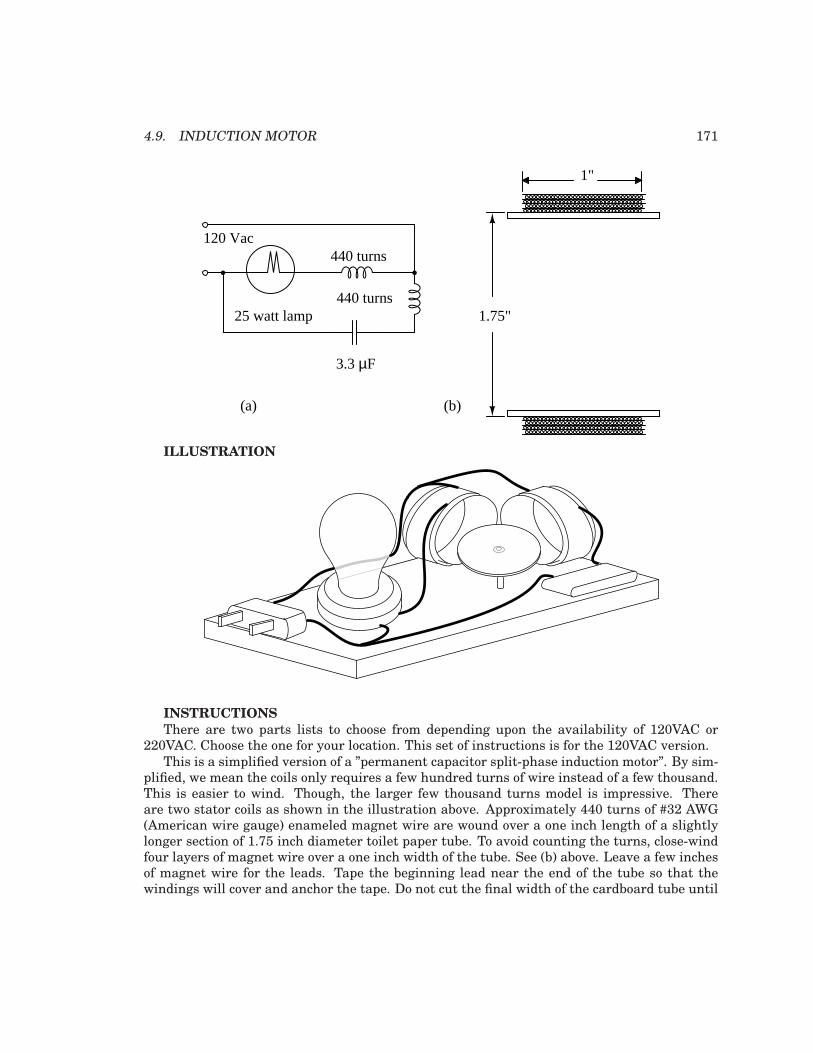
4.9. INDUCTION MOTOR 171
1"
1.75"
3.3 µF
440 turns
440 turns
120 Vac
25 watt lamp
(a) (b)
ILLUSTRATION
INSTRUCTIONS
There are two parts lists to choose from depending upon the availability of 120VAC or220VAC. Choose the one for your location. This set of instructions is for the 120VAC version.
This is a simplified version of a ”permanent capacitor split-phase induction motor”. By sim-plified, we mean the coils only requires a few hundred turns of wire instead of a few thousand.This is easier to wind. Though, the larger few thousand turns model is impressive. Thereare two stator coils as shown in the illustration above. Approximately 440 turns of #32 AWG(American wire gauge) enameled magnet wire are wound over a one inch length of a slightlylonger section of 1.75 inch diameter toilet paper tube. To avoid counting the turns, close-windfour layers of magnet wire over a one inch width of the tube. See (b) above. Leave a few inchesof magnet wire for the leads. Tape the beginning lead near the end of the tube so that thewindings will cover and anchor the tape. Do not cut the final width of the cardboard tube until

172 CHAPTER 4. AC CIRCUITS
the winding is finished. Close wind a single layer. Tape or cement the first layer to prevent un-winding before proceeding to the second layer. Though it is possible to wind additional layersdirectly over existing layers, consider applying tape or paper between the layers as shown inschematic (b). After four layers are wound, glue the windings in place.
If close winding four layers of magnet wire it too difficult, scramble wind 440 turns of themagnet wire over the end of the cardboard tube. However, the close-wound style coil mountsmore easily to the baseboard. Keep the windings within a one inch length.
Cut the finished winding from the end of the cardboard tube with a razor knife allowingthe form to extend a little beyond the winding. Strip the enamel from an inch off the ends ofthe pair of lead wires with sandpaper. Splice the bare ends to heavier gauge insulated hook-upwire. Solder the splice. Insulate with tape or heat-shrink tubing. Secure the splice to the coilbody. Then proceed with a second identical coil.
Refer to both the schematic diagram and the illustration for assembly. Note that the coilsare mounted at right angles. They may be cemented to an insulating baseboard like wood. The25 watt lamp is wired in series with one coil. This limits the current flowing through the coil.The lamp is a substitute for an 820 Ω power resistor. The capacitor is wired in series with theother coil. It also limits the current through the coil. In addition, it provides a leading phaseshift of the current with respect to voltage. The schematic and illustration show no powerswitch or fuse. Add these if desired.
The rotor must be made of a ferromagnetic material like a steel can lid or bottle cap. Theillustration below shows how to make the rotor. Select a circular rotor either smaller than thecoil forms or a little larger. Use geometry to locate and mark the center. The center needs to bedimpled. Select an eighth inch diameter (a few mm) nail (a) and file or grind the point roundas shown at (b). Place the rotor atop a piece of soft wood (c) and hammer the rounded pointinto the center (d). Practice on a piece of similar scrap metal. Take care not to pierce the rotor.A dished rotor (f) or a lid (g) balance better than the flat rotor (e). The pivot point (e) may bea straight pin driven through a movable wooden pedestal, or through the main board. The tipof a ball-point pen also works. If the rotor does not balance atop the pivot, remove metal fromthe heavy side.
(a) (b) (c) (d) (e)
(f)
(g)
Double check the wiring. Check that any bare wire has been insulated. The circuit maybe powered-up without the rotor. The lamp should light. Both coils will warm within a fewminutes. Excessive heating means that a lower wattage (higher resistance) lamp and a lowervalue capacitor should be substituted in series with the respective coils.

4.9. INDUCTION MOTOR 173
Place the rotor atop the pivot and move it between both coils. It should spin. The closer itis, the faster it should spin. Both coils should be warm, indicating power. Try different sizeand style rotors. Try a small rotor on the opposite side of the coils compared to the illustration.
For lack of #32 AWG magnet wire try 440 turns of slightly a larger diameter (lesser AWGnumber) wire. This will require more than 4 layers for the required turns. A night-light fixturemight be less expensive than the full-size lamp socket illustrated. Though night-light bulbs aretoo low a wattage at 3 or 7 watts, 15 watt bulbs fit the socket.

174 CHAPTER 4. AC CIRCUITS
4.10 Induction motor, large
PARTS AND MATERIALS
• AC power source: 120VAC
• Capacitor, 3.3 µF 120VAC or 350VDC, non-polarized
• #33 AWG magnet wire, 2 pounds
• wooden board approx. 6 to 12 in. square.
• AC line cord with plug
• 5.1 inch dia. plastic 3 liter soda bottle
• discarded ballpoint pen
• misc. small wood blocks
CROSS-REFERENCES
Lessons In Electric Circuits, Volume 2, chapter 13: ”AC motors”, ”Single Phase inductionmotors”,”Permanent split-capacitor motor”.
LEARNING OBJECTIVES
• To build a large exhibit size AC permanent split-capacitor induction motor.
• To illustrate the simplicity of the AC induction motor.
SCHEMATIC DIAGRAM
1"
3.3 µF
3200 turns
3800 turns
120 Vac
(a) (b)
L1
L2
C1
5.1 in.

4.10. INDUCTION MOTOR, LARGE 175
ILLUSTRATION
C1
L1L2
INSTRUCTIONS
This is a larger version of a ”permanent capacitor split-phase induction motor”. There aretwo different stator coils. The 1.0 inch wide 3200 turn L2 winding is shown in the illustrationabove (b), wound over a section of 5.1 inch diameter plastic 3-liter soda bottle. L1 is approx-imately 3800 turns of #33 AWG (American wire gauge) enameled magnet wire wound over a1.25 width of a section of soda bottle, wider than shown at (b). Mark a 1.25 inch wide cylinderwith 0.25 inch margins on each end. The wire will be wound on the 1.25 inch zone. The formis cut from the bottle on the outside edges of the margin. Cuts of 0.25 inch from the marginto winding zone are spaced at 1 inch intervals around the circumference of both ends so thatthe margin may be bent up at 90o to hold the wire on the form. To avoid counting the 3800turns, scramble wind a 1/8 inch thickness of magnet wire over the one inch width of the form.Else, count the turns. Scrape the enamel from 1-inch on the free end, and scrape only a smallsection from the lead to the spool. Do NOT cut the lead to the spool. Measure the resistance,and estimate how much more wire to wind to achieve 894 Ω. Apply enamel, nail polish, tape,or other insulation to the bare spot on the spool lead. Continue winding, and recheck the resis-tance. Once the approximate 894 Ω is achieved, leave a few inches of magnet wire for the lead.Cut the lead from the spool. Secure the windings to the form with lacing twine or other means.
The L1 winding of 3200 turns is approximately 744 Ω and is wound on a 1.0 inch wide formas shown at (b) in a manner similar to the previous L2 winding.
Strip the enamel off 1-inch of the ends of magnet wire leads if not already done. Splice thebare ends to heavier gauge insulated hook-up wire. Solder the splice. Insulate with tape orheat-shrink tubing. Secure the splice to the coil body. Then proceed with the second coil. Thecoils may be mounted in one corner of the wooden base. Alternatively, for more flexability inuse, they may be mounted to movable pallets.
Refer to both the schematic diagram and the illustration for assembly. Note that the coilsare mounted at right angles. L2, the smaller coil is wired to both sides of the 120 Vac line. Thecapacitor is wired in series with the wider coil L1. The capacitor provides a leading phase shiftof the current with respect to voltage. The schematic and illustration show no power switch orfuse. Add these additions are recommended.

176 CHAPTER 4. AC CIRCUITS
If this device is intended for use by non-technicians as an unsupervised exhibit, all exposedbare terminations like the capacitor must be made finger safe by covering with shields. Theswitch and fuse mentioned above are necessary. Finally, the enamel on the coils only provides asingle layer of insulation. For safety, a second layer such as an insulating wrapping, Plexiglasbox, or other means is called for. Replace all wooden components with Plexiglas for superiorfire safety in an unsupervised exhibit.
The rotor must be made of a ferromagnetic material like a steel vegetable can, fruitcakecan, etc. A too long vegetable can may be cut in half. The illustration for the previous smallinduction motor shows rotor dimpled bearing and pivot details. The rotor may be smaller thanthe coil forms as in the case of a cut down vegetable can. It can even be as small as the canlid rotor used with the previous small motor. It is also possible to drive a rotor larger thanthe coils, which is the case with the fruitcake can. Locate and mark the center of the rotor.The center needs to be dimpled. Select an eighth inch diameter (a few mm) nail (a) and fileor grind the point round. Use this and a block of wood to dimple the rotor as shown in theprevious small motor A fairly long can balances better than a flat rotor due to the lower centerof gravity. The tip of a ball point pen works well as a pivot for larger rotors. Mount the pivot toa movable wooden pedestal.
Double check the wiring. Check that any bare wire has been insulated. The circuit may bepowered-up without the rotor. Excessive heating in L2 indicates that more turns are required.Excessive heat in L1 calls for a reduction in the capacitance of C1. No heat at all indicatesindicates an open circuit to the affected coil.
Place the rotor atop the pivot and move it between both energized coils. It should spin.The closer it is, the faster it should spin. Both coils should be warm, indicating power. Trydifferent size and style rotors. Try a small rotor on the opposite side of the coils compared tothe illustration.
Three models of this motor have been built using #33 AWG magnet wire because a largespool was on hand. AWG #32 magnet wire is probably easier to get. It should work. Althoughthe current will be higher due to the lower resistance of the larger diameter #32 wire. If a3.3µF capacitor is not available, use somenting close as long as it has an adequate voltagerating. A discarded AC motor run capacitor (bath tub shaped) was used by the author. Do nouse a motor start capacitor (black cylinder). These are only usable for a few seconds of motorstarting, and may explode if used longer than that.
Try this: It is possible to simultaneously spin more than one rotor. For example, inaddition to the main rotor inside the right angle formed by the coils, place a second smallerrotor (can or bottle lid) near the pair of coils outside the right angle at the vertex.
It is possible to reverse the direction of rotation by reversing one of the coils. If the coils aremounted to movable pallets, rotate one coil 180o. Another method, especially usefull with fixedcoils, is to wire one of the coils to a DPDT polarity reversing switch. For example, disconnectL2 and wire it to the wipers (center contacts) of the DPDT switch. The top contacts go to the120 Vac. The top contacts also go to the the bottom contacts in an X-crossover pattern.

4.11. PHASE SHIFT 177
4.11 Phase shift
PARTS AND MATERIALS
• Low-voltage AC power supply
• Two capacitors, 0.1 µF each, non-polarized (Radio Shack catalog # 272-135)
• Two 27 kΩ resistors
I recommend ceramic disk capacitors, because they are insensitive to polarity (non-polarized),inexpensive, and durable. Avoid capacitors with any kind of polarity marking, as these will bedestroyed when powered by AC!
CROSS-REFERENCES
Lessons In Electric Circuits, Volume 2, chapter 1: ”Basic AC Theory”
Lessons In Electric Circuits, Volume 2, chapter 4: ”Reactance and Impedance – Capacitive”
LEARNING OBJECTIVES
• How out-of-phase AC voltages do not add algebraically, but according to vector (phasor)arithmetic
SCHEMATIC DIAGRAM
12 VRMS
R1
R2
C1
C2
27 kΩ
27 kΩ
0.1 µF
0.1 µF
ILLUSTRATION

178 CHAPTER 4. AC CIRCUITS
Low-voltage AC power supply
6 612
R1R2C1C2
INSTRUCTIONS
Build the circuit and measure voltage drops across each component with an AC voltmeter.Measure total (supply) voltage with the same voltmeter. You will discover that the voltagedrops do not add up to equal the total voltage. This is due to phase shifts in the circuit: voltagedropped across the capacitors is out-of-phase with voltage dropped across the resistors, andthus the voltage drop figures do not add up as one might expect. Taking phase angle intoconsideration, they do add up to equal the total, but a voltmeter doesn’t provide phase anglemeasurements, only amplitude.
Try measuring voltage dropped across both resistors at once. This voltage drop will equalthe sum of the voltage drops measured across each resistor separately. This tells you that boththe resistors’ voltage drop waveforms are in-phase with each other, since they add simply anddirectly.
Measure voltage dropped across both capacitors at once. This voltage drop, like the dropmeasured across the two resistors, will equal the sum of the voltage drops measured acrosseach capacitor separately. Likewise, this tells you that both the capacitors’ voltage drop wave-forms are in-phase with each other.
Given that the power supply frequency is 60 Hz (household power frequency in the UnitedStates), calculate impedances for all components and determine all voltage drops using Ohm’sLaw (E=IZ ; I=E/Z ; Z=E/I). The polar magnitudes of the results should closely agree with yourvoltmeter readings.
COMPUTER SIMULATION
Schematic with SPICE node numbers:

4.11. PHASE SHIFT 179
R1
R2
C1
C2
27 kΩ
27 kΩ
0.1 µF
0.1 µF
V1
1
0 0
1
2
3
4
Rbogus1
Rbogus2
3
4
0
The two large-value resistors Rbogus1 and Rbogus1 are connected across the capacitors toprovide a DC path to ground in order that SPICE will work. This is a ”fix” for one of SPICE’squirks, to avoid it from seeing the capacitors as open circuits in its analysis. These two resistorsare entirely unnecessary in the real circuit.
Netlist (make a text file containing the following text, verbatim):phase shiftv1 1 0 ac 12 sinr1 1 2 27kr2 2 3 27kc1 3 4 0.1uc2 4 0 0.1urbogus1 3 4 1e9rbogus2 4 0 1e9.ac lin 1 60 60
* Voltage across each component:.print ac v(1,2) v(2,3) v(3,4) v(4,0)
* Voltage across pairs of similar components.print ac v(1,3) v(3,0).end

180 CHAPTER 4. AC CIRCUITS
4.12 Sound cancellation
PARTS AND MATERIALS
• Low-voltage AC power supply
• Two audio speakers
• Two 220 Ω resistors
Large, low-frequency (”woofer”) speakers are most appropriate for this experiment. Foroptimum results, the speakers should be identical and mounted in enclosures.
CROSS-REFERENCES
Lessons In Electric Circuits, Volume 2, chapter 1: ”Basic AC Theory”
LEARNING OBJECTIVES
• How phase shift can cause waves to either reinforce or interfere with each other
• The importance of speaker ”phasing” in stereo systems
SCHEMATIC DIAGRAM
220 Ω
220 Ω
12 V
ILLUSTRATION

4.12. SOUND CANCELLATION 181
Low-voltage AC power supply
6 612
Speaker Speaker
INSTRUCTIONS
Connect each speaker to the low-voltage AC power supply through a 220 Ω resistor. Theresistor limits the amount of power delivered to each speaker by the power supply. A low-pitched, 60-Hertz tone should be heard from the speakers. If the tone sounds too loud, usehigher-value resistors.
With both speakers connected and producing sound, position them so that they are only afoot or two away, facing toward each other. Listen to the volume of the 60-Hertz tone. Now,reverse the connections (the ”polarity”) of just one of the speakers and note the volume again.Try switching the polarity of one speaker back and forth from original to reversed, comparingvolume levels each way. What do you notice?
By reversing wire connections to one speaker, you are reversing the phase of that speaker’ssound wave in reference to the other speaker. In one mode, the sound waves will reinforce oneanother for a strong volume. In the other mode, the sound waves will destructively interfere,resulting in diminished volume. This phenomenon is common to all wave events: sound waves,electrical signals (voltage ”waves”), waves in water, and even light waves!
Multiple speakers in a stereo sound system must be properly ”phased” so that their respec-tive sound waves don’t cancel each other, leaving less total sound level for the listener(s) tohear. So, even in an AC system where there really is no such thing as constant ”polarity,” thesequence of wire connections may make a significant difference in system performance.
This principle of volume reduction by destructive interference may be exploited for noisecancellation. Such systems sample the waveform of the ambient noise, then produce an iden-

182 CHAPTER 4. AC CIRCUITS
tical sound signal 180o out of phase with the noise. When the two sound signals meet, theycancel each other out, ideally eliminating all the noise. As one might guess, this is much easieraccomplished with noise sources of steady frequency and amplitude. Cancellation of random,broad-spectrum noise is very difficult, as some sort of signal-processing circuit must samplethe noise and generate precisely the right amount of cancellation sound at just the right timein order to be effective.

4.13. MUSICAL KEYBOARD AS A SIGNAL GENERATOR 183
4.13 Musical keyboard as a signal generator
PARTS AND MATERIALS
• Electronic ”keyboard” (musical)
• ”Mono” (not stereo) headphone-type plug
• Impedance matching transformer (1k Ω to 8 Ω ratio; Radio Shack catalog # 273-1380)
• 10 kΩ resistor
In this experiment, you’ll learn how to use an electronic musical keyboard as a source ofvariable-frequency AC voltage signals. You need not purchase an expensive keyboard for this– but one with at least a few dozen ”voice” selections (piano, flute, harp, etc.) would be good.The ”mono” plug will be plugged into the headphone jack of the musical keyboard, so get a plugthat’s the correct size for the keyboard.
The ”impedance matching transformer” is a small-size transformer easily obtained from anelectronics supply store. One may be scavenged from a small, junk radio: it connects betweenthe speaker and the circuit board (amplifier), so is easily identifiable by location. The primarywinding is rated in ohms of impedance (1000 Ω), and is usually center-tapped. The secondarywinding is 8 Ω and not center-tapped. These impedance figures are not the same as DC re-sistance, so don’t expect to read 1000 Ω and 8 Ω with your ohmmeter – however, the 1000 Ω
winding will read more resistance than the 8 Ω winding, because it has more turns.If such a transformer cannot be obtained for the experiment, a regular 120V/6V step-down
power transformer works fairly well, too.
CROSS-REFERENCES
Lessons In Electric Circuits, Volume 2, chapter 1: ”Basic AC Theory”Lessons In Electric Circuits, Volume 2, chapter 7: ”Mixed-Frequency AC Signals”
LEARNING OBJECTIVES
• Difference between amplitude and frequency
• Measuring AC voltage, current with a meter
• Transformer operation, step-up
SCHEMATIC DIAGRAM
Keyboard
plug8 Ω 1 kΩ
10 kΩ

184 CHAPTER 4. AC CIRCUITS
ILLUSTRATION
Volume"Voice" selection
plug
1000 Ω
8 ΩCOMA
V
V A
AOFF
INSTRUCTIONS
Normally, a student of electronics in a school would have access to a device called a signal
generator, or function generator, used to make variable-frequency voltage waveforms to powerAC circuits. An inexpensive electronic keyboard is a cheaper alternative to a regular signalgenerator, and provides features that most signal generators cannot match, such as producingmixed-frequency waves.
To ”tap in” to the AC voltage produced by the keyboard, you’ll need to insert a plug into theheadphone jack (sometimes just labeled ”phone” on the keyboard) complete with two wires forconnection to circuits of your own design. When you insert the plug into the jack, the normalspeaker built in to the keyboard will be disconnected (assuming the keyboard is equipped withone), and the signal that used to power that speaker will be available at the plug wires. In

4.13. MUSICAL KEYBOARD AS A SIGNAL GENERATOR 185
this particular experiment, I recommend using the keyboard to power the 8 Ω side of an audio”output” transformer to step up voltage to a higher level. If using a power transformer insteadof an audio output transformer, connect the keyboard to the low-voltage winding so that itoperates as a step-up device. Keyboards produce very low voltage signals, so there is no shockhazard in this experiment.
Using an inexpensive Yamaha keyboard, I have found that the ”panflute” voice setting pro-duces the truest sine-wave waveform. This waveform, or something close to it (flute, for ex-ample), is recommended to start experimenting with since it is relatively free of harmonics(many waveforms mixed together, of integer-multiple frequency). Being composed of just onefrequency, it is a less complex waveform for your multimeter to measure. Make sure the key-board is set to a mode where the note will be sustained as any key is held down – otherwise,the amplitude (voltage) of the waveform will be constantly changing (high when the key is firstpressed, then decaying rapidly to zero).
Using an AC voltmeter, read the voltage direct from the headphone plug. Then, read thevoltage as stepped up by the transformer, noting the step ratio. If your multimeter has a ”fre-quency” function, use it to measure the frequency of the waveform produced by the keyboard.Try different notes on the keyboard and record their frequencies. Do you notice a pattern infrequency as you activate different notes, especially keys that are similar to each other (noticethe 12-key black-and-white pattern repeated on the keyboard from left to right)? If you don’tmind making marks on your keyboard, write the frequencies in Hertz in black ink on the whitekeys, near the tops where fingers are less likely to rub the numbers off.
Ideally, there should be no change in signal amplitude (voltage) as different frequencies(notes on the keyboard) are tried. If you adjust the volume up and down, you should discoverthat changes in amplitude should have little or no impact on frequency measurement. Ampli-tude and frequency are two completely independent aspects of an AC signal.
Try connecting the keyboard output to a 10 kΩ load resistance (through the headphoneplug), and measure AC current with your multimeter. If your multimeter has a frequencyfunction, you can measure the frequency of this current as well. It should be the same as forthe voltage for any given note (keyboard key).

186 CHAPTER 4. AC CIRCUITS
4.14 PC Oscilloscope
PARTS AND MATERIALS
• IBM-compatible personal computer with sound card, running Windows 3.1 or better
• Winscope software, downloaded free from internet
• Electronic ”keyboard” (musical)
• ”Mono” (not stereo) headphone-type plug for keyboard
• ”Mono” (not stereo) headphone-type plug for computer sound card microphone input
• 10 kΩ potentiometer
The Winscope program I’ve used was written by Dr. Constantin Zeldovich, for free personaland academic use. It plots waveforms on the computer screen in response to AC voltage signalsinterpreted by the sound card microphone input. A similar program, called Oscope, is madefor the Linux operating system. If you don’t have access to either software, you may use the”sound recorder” utility that comes stock with most versions of Microsoft Windows to displaycrude waveshapes.
CROSS-REFERENCES
Lessons In Electric Circuits, Volume 2, chapter 7: ”Mixed-Frequency AC Signals”
Lessons In Electric Circuits, Volume 2, chapter 12: ”AC Metering Circuits”
LEARNING OBJECTIVES
• Computer use
• Basic oscilloscope function
SCHEMATIC DIAGRAM
Keyboard
plug
10 kΩ
Computer
plug
ILLUSTRATION

4.14. PC OSCILLOSCOPE 187
Volume"Voice" selection
plug
Computer
mic. input
Monitor
plug
INSTRUCTIONS
The oscilloscope is an indispensable test instrument for the electronics student and profes-sional. No serious electronics lab should be without one (or two!). Unfortunately, commercialoscilloscopes tend to be expensive, and it is almost impossible to design and build your ownwithout another oscilloscope to troubleshoot it! However, the sound card of a personal com-puter is capable of ”digitizing” low-voltage AC signals from a range of a few hundred Hertz toseveral thousand Hertz with respectable resolution, and free software is available for display-ing these signals in oscilloscope form on the computer screen. Since most people either havea personal computer or can obtain one for less cost than an oscilloscope, this becomes a viablealternative for the experimenter on a budget.
One word of caution: you can cause significant hardware damage to your computer
if signals of excessive voltage are connected to the sound card’s microphone input!
The AC voltages produced by a musical keyboard are too low to cause damage to your computerthrough the sound card, but other voltage sources might be hazardous to your computer’shealth. Use this ”oscilloscope” at your own risk!
Using the keyboard and plug arrangement described in the previous experiment, connectthe keyboard output to the outer terminals of a 10 kΩ potentiometer. Solder two wires to theconnection points on the sound card microphone input plug, so that you have a set of ”testleads” for the ”oscilloscope.” Connect these test leads to the potentiometer: between the middleterminal (the wiper) and either of the outer terminals.
Start the Winscope program and click on the ”arrow” icon in the upper-left corner (it lookslike the ”play” arrow seen on tape player and CD player control buttons). If you press a key onthe musical keyboard, you should see some kind of waveform displayed on the screen. Choosethe ”panflute” or some other flute-like voice on the musical keyboard for the best sine-waveshape. If the computer displays a waveform that looks kind of like a square wave, you need toadjust the potentiometer for a lower-amplitude signal. Almost any waveshape will be ”clipped”to look like a square wave if it exceeds the amplitude limit of the sound card.

188 CHAPTER 4. AC CIRCUITS
Test different instrument ”voices” on the musical keyboard and note the different wave-shapes. Note how complex some of the waveshapes are, compared to the panflute voice. Ex-periment with the different controls in the Winscope window, noting how they change theappearance of the waveform.
As a test instrument, this ”oscilloscope” is quite poor. It has almost no capability to makeprecision measurements of voltage, although its frequency precision is surprisingly good. It isvery limited in the ranges of voltage and frequency it can display, relegating it to the analysisof low- and mid-range audio tones. I have had very little success getting the ”oscilloscope” todisplay good square waves, presumably because of its limited frequency response. Also, thecoupling capacitor found in sound card microphone input circuits prevents it from measuringDC voltage: it is as though the ”AC coupling” feature of a normal oscilloscope were stuck ”on.”
Despite these shortcomings, it is useful as a demonstration tool, and for initial explorationsinto waveform analysis for the beginning student of electronics. For those who are interested,there are several professional-quality oscilloscope adapter devices manufactured for personalcomputers whose performance is far beyond that of a sound card, and they are typically sold atless cost than a complete stand-alone oscilloscope (around $400, year 2002). Radio Shack sellsone made by Velleman, catalog # 910-3914. Having a computer serve as the display mediumbrings many advantages, not the least of which is the ability to easily store waveform picturesas digital files.

4.15. WAVEFORM ANALYSIS 189
4.15 Waveform analysis
PARTS AND MATERIALS
• IBM-compatible personal computer with sound card, running Windows 3.1 or better
• Winscope software, downloaded free from internet
• Electronic ”keyboard” (musical)
• ”Mono” (not stereo) headphone-type plug for keyboard
• ”Mono” (not stereo) headphone-type plug for computer sound card microphone input, withwires for connecting to voltage sources
• 10 kΩ potentiometer
Parts and equipment for this experiment are identical to those required for the ”PC oscillo-scope” experiment.
CROSS-REFERENCES
Lessons In Electric Circuits, Volume 2, chapter 7: ”Mixed-Frequency AC Signals”
LEARNING OBJECTIVES
• Understand the difference between time-domain and frequency-domain plots
• Develop a qualitative sense of Fourier analysis
SCHEMATIC DIAGRAM
Keyboard
plug
10 kΩ
Computer
plug
ILLUSTRATION

190 CHAPTER 4. AC CIRCUITS
Volume"Voice" selection
plug
Computer
mic. input
Monitor
plug
INSTRUCTIONS
TheWinscope program comes with another feature other than the typical ”time-domain” os-cilloscope display: ”frequency-domain” display, which plots amplitude (vertical) over frequency(horizontal). An oscilloscope’s ”time-domain” display plots amplitude (vertical) over time (hor-izontal), which is fine for displaying waveshape. However, when it is desirable to see theharmonic constituency of a complex wave, a frequency-domain plot is the best tool.
If using Winscope, click on the ”rainbow” icon to switch to frequency-domain mode. Gen-erate a sine-wave signal using the musical keyboard (panflute or flute voice), and you shouldsee a single ”spike” on the display, corresponding to the amplitude of the single-frequency sig-nal. Moving the mouse cursor beneath the peak should result in the frequency being displayednumerically at the bottom of the screen.
If two notes are activated on the musical keyboard, the plot should show two distinct peaks,each one corresponding to a particular note (frequency). Basic chords (three notes) producethree spikes on the frequency-domain plot, and so on. Contrast this with normal oscilloscope(time-domain) plot by clicking once again on the ”rainbow” icon. A musical chord displayed intime-domain format is a very complex waveform, but is quite simple to resolve into constituentnotes (frequencies) on a frequency-domain display.
Experiment with different instrument ”voices” on the musical keyboard, correlating thetime-domain plot with the frequency-domain plot. Waveforms that are symmetrical above andbelow their centerlines contain only odd-numbered harmonics (odd-integer multiples of thebase, or fundamental frequency), while nonsymmetrical waveforms contain even-numberedharmonics as well. Use the cursor to locate the specific frequency of each peak on the plot, anda calculator to determine whether each peak is even- or odd-numbered.

4.16. INDUCTOR-CAPACITOR ”TANK” CIRCUIT 191
4.16 Inductor-capacitor ”tank” circuit
PARTS AND MATERIALS
• Oscilloscope
• Assortment of non-polarized capacitors (0.1 µF to 10 µF)
• Step-down power transformer (120V / 6 V)
• 10 kΩ resistors
• Six-volt battery
The power transformer is used simply as an inductor, with only one winding connected. Theunused winding should be left open. A simple iron core, single-winding inductor (sometimesknown as a choke) may also be used, but such inductors are more difficult to obtain than powertransformers.
CROSS-REFERENCES
Lessons In Electric Circuits, Volume 2, chapter 6: ”Resonance”
LEARNING OBJECTIVES
• How to build a resonant circuit
• Effects of capacitor size on resonant frequency
• How to produce antiresonance
SCHEMATIC DIAGRAM
L C
ILLUSTRATION

192 CHAPTER 4. AC CIRCUITS
+-
touchclips
together
(transformer used as an inductor)
INSTRUCTIONS
If an inductor and a capacitor are connected in parallel with each other, and then brieflyenergized by connection to a DC voltage source, oscillations will ensue as energy is exchangedfrom the capacitor to inductor and vice versa. These oscillations may be viewed with an os-cilloscope connected in parallel with the inductor/capacitor circuit. Parallel inductor/capacitorcircuits are commonly known as tank circuits.
Important note: I recommend against using a PC/sound card as an oscilloscope for thisexperiment, because very high voltages can be generated by the inductor when the battery isdisconnected (inductive ”kickback”). These high voltages will surely damage the sound card’sinput, and perhaps other portions of the computer as well.
A tank circuit’s natural frequency, called the resonant frequency, is determined by the sizeof the inductor and the size of the capacitor, according to the following equation:
fresonant = 2π LC
1
Many small power transformers have primary (120 volt) winding inductances of approx-imately 1 H. Use this figure as a rough estimate of inductance for your circuit to calculateexpected oscillation frequency.
Ideally, the oscillations produced by a tank circuit continue indefinitely. Realistically, os-cillations will decay in amplitude over the course of several cycles due to the resistive andmagnetic losses of the inductor. Inductors with a high ”Q” rating will, of course, produce longer-lasting oscillations than low-Q inductors.
Try changing capacitor values and noting the effect on oscillation frequency. You mightnotice changes in the duration of oscillations as well, due to capacitor size. Since you knowhow to calculate resonant frequency from inductance and capacitance, can you figure out away to calculate inductor inductance from known values of circuit capacitance (as measuredby a capacitance meter) and resonant frequency (as measured by an oscilloscope)?
Resistance may be intentionally added to the circuit – either in series or parallel – for theexpress purpose of dampening oscillations. This effect of resistance dampening tank circuit

4.16. INDUCTOR-CAPACITOR ”TANK” CIRCUIT 193
oscillation is known as antiresonance. It is analogous to the action of a shock absorber indampening the bouncing of a car after striking a bump in the road.
COMPUTER SIMULATION
Schematic with SPICE node numbers:
L1 C1
1
0 0
2Rstray
Rstray is placed in the circuit to dampen oscillations and produce a more realistic simula-tion. A lower Rstray value causes longer-lived oscillations because less energy is dissipated.Eliminating this resistor from the circuit results in endless oscillation.
Netlist (make a text file containing the following text, verbatim):tank circuit with lossl1 1 0 1 ic=0rstray 1 2 1000c1 2 0 0.1u ic=6.tran 0.1m 20m uic.plot tran v(1,0).end

194 CHAPTER 4. AC CIRCUITS
4.17 Signal coupling
PARTS AND MATERIALS
• 6 volt battery
• One capacitor, 0.22 µF (Radio Shack catalog # 272-1070 or equivalent)
• One capacitor, 0.047 µF (Radio Shack catalog # 272-134 or equivalent)
• Small ”hobby” motor, permanent-magnet type (Radio Shack catalog # 273-223 or equiva-lent)
• Audio detector with headphones
• Length of telephone cable, several feet long (Radio Shack catalog # 278-872)
Telephone cable is also available from hardware stores. Any unshielded multiconductorcable will suffice for this experiment. Cables with thin conductors (telephone cable is typically24-gauge) produce a more pronounced effect.
CROSS-REFERENCES
Lessons In Electric Circuits, Volume 2, chapter 7: ”Mixed-Frequency AC Signals”
Lessons In Electric Circuits, Volume 2, chapter 8: ”Filters”
LEARNING OBJECTIVES
• How to ”couple” AC signals and block DC signals to a measuring instrument
• How stray coupling happens in cables
• Techniques to minimize inter-cable coupling
SCHEMATIC DIAGRAM
Mtr
Telephone cable
ILLUSTRATION

4.17. SIGNAL COUPLING 195
+-
plug
headphones
Sensitivity
Telephonecable
Motor
INSTRUCTIONS
Connect the motor to the battery using two of the telephone cable’s four conductors. Themotor should run, as expected. Now, connect the audio signal detector across the motor termi-nals, with the 0.047 µF capacitor in series, like this:

196 CHAPTER 4. AC CIRCUITS
+-
plug
headphones
Sensitivity
You should be able to hear a ”buzz” or ”whine” in the headphones, representing the AC”noise” voltage produced by the motor as the brushes make and break contact with the rotatingcommutator bars. The purpose of the series capacitor is to act as a high-pass filter, so that thedetector only receives the AC voltage across the motor’s terminals, not any DC voltage. This isprecisely how oscilloscopes provide an ”AC coupling” feature for measuring the AC content ofa signal without any DC bias voltage: a capacitor is connected in series with one test probe.
Ideally, one would expect nothing but pure DC voltage at the motor’s terminals, becausethe motor is connected directly in parallel with the battery. Since the motor’s terminals areelectrically common with the respective terminals of the battery, and the battery’s nature is tomaintain a constant DC voltage, nothing but DC voltage should appear at the motor terminals,right? Well, because of resistance internal to the battery and along the conductor lengths,current pulses drawn by the motor produce oscillating voltage ”dips” at the motor terminals,causing the AC ”noise” heard by the detector:

4.17. SIGNAL COUPLING 197
Motor
Rwire
Rwire
Battery
Use the audio detector to measure ”noise” voltage directly across the battery. Since the ACnoise is produced in this circuit by pulsating voltage drops along stray resistances, the lessresistance we measure across, the less noise voltage we should detect:
+-
plug
headphones
Sensitivity
You may also measure noise voltage dropped along either of the telephone cable conductorssupplying power to the motor, by connecting the audio detector between both ends of a singlecable conductor. The noise detected here originates from current pulses through the resistanceof the wire:

198 CHAPTER 4. AC CIRCUITS
+-
plug
headphones
Sensitivity
Now that we have established how AC noise is created and distributed in this circuit, let’sexplore how it is coupled to adjacent wires in the cable. Use the audio detector to measurevoltage between one of the motor terminals and one of the unused wires in the telephone cable.The 0.047 µF capacitor is not needed in this exercise, because there is no DC voltage betweenthese points for the detector to detect anyway:
+-
plug
headphones
Sensitivity

4.17. SIGNAL COUPLING 199
The noise voltage detected here is due to stray capacitance between adjacent cable con-ductors creating an AC current ”path” between the wires. Remember that no current actuallygoes through a capacitance, but the alternate charging and discharging action of a capacitance,whether it be intentional or unintentional, provides alternating current a pathway of sorts.
If we were to try and conduct a voltage signal between one of the unused wires and a pointcommon with the motor, that signal would become tainted with noise voltage from the motor.This could be quite detrimental, depending on how much noise was coupled between the twocircuits and how sensitive one circuit was to the other’s noise. Since the primary couplingphenomenon in this circuit is capacitive in nature, higher-frequency noise voltages are morestrongly coupled than lower-frequency noise voltages.
If the additional signal was a DC signal, with no AC expected in it, we could mitigatethe problem of coupled noise by ”decoupling” the AC noise with a relatively large capacitorconnected across the DC signal’s conductors. Use the 0.22 µF capacitor for this purpose, asshown:
+-
plug
headphones
Sensitivity
"decoupling"capacitor
The decoupling capacitor acts as a practical short-circuit to any AC noise voltage, whilenot affecting DC voltage signals between those two points at all. So long as the decouplingcapacitor value is significantly larger than the stray ”coupling” capacitance between the cable’sconductors, the AC noise voltage will be held to a minimum.
Another way of minimizing coupled noise in a cable is to avoid having two circuits sharea common conductor. To illustrate, connect the audio detector between the two unused wiresand listen for a noise signal:

200 CHAPTER 4. AC CIRCUITS
+-
plug
headphones
Sensitivity
There should be far less noise detected between any two of the unused conductors thanbetween one unused conductor and one used in the motor circuit. The reason for this drasticreduction in noise is that stray capacitance between cable conductors tends to couple the same
noise voltage to both of the unused conductors in approximately equal proportions. Thus,when measuring voltage between those two conductors, the detector only ”sees” the differencebetween two approximately identical noise signals.

Chapter 5
DISCRETE SEMICONDUCTOR
CIRCUITS
Contents
5.1 Introduction . . . . . . . . . . . . . . . . . . . . . . . . . . . . . . . . . . . . . . 202
5.2 Commutating diode . . . . . . . . . . . . . . . . . . . . . . . . . . . . . . . . . 203
5.3 Half-wave rectifier . . . . . . . . . . . . . . . . . . . . . . . . . . . . . . . . . . 205
5.4 Full-wave center-tap rectifier . . . . . . . . . . . . . . . . . . . . . . . . . . . 213
5.5 Full-wave bridge rectifier . . . . . . . . . . . . . . . . . . . . . . . . . . . . . . 218
5.6 Rectifier/filter circuit . . . . . . . . . . . . . . . . . . . . . . . . . . . . . . . . 221
5.7 Voltage regulator . . . . . . . . . . . . . . . . . . . . . . . . . . . . . . . . . . . 227
5.8 Transistor as a switch . . . . . . . . . . . . . . . . . . . . . . . . . . . . . . . . 230
5.9 Static electricity sensor . . . . . . . . . . . . . . . . . . . . . . . . . . . . . . . 235
5.10 Pulsed-light sensor . . . . . . . . . . . . . . . . . . . . . . . . . . . . . . . . . . 238
5.11 Voltage follower . . . . . . . . . . . . . . . . . . . . . . . . . . . . . . . . . . . . 241
5.12 Common-emitter amplifier . . . . . . . . . . . . . . . . . . . . . . . . . . . . . 246
5.13 Multi-stage amplifier . . . . . . . . . . . . . . . . . . . . . . . . . . . . . . . . . 251
5.14 Current mirror . . . . . . . . . . . . . . . . . . . . . . . . . . . . . . . . . . . . 255
5.15 JFET current regulator . . . . . . . . . . . . . . . . . . . . . . . . . . . . . . . 261
5.16 Differential amplifier . . . . . . . . . . . . . . . . . . . . . . . . . . . . . . . . 266
5.17 Simple op-amp . . . . . . . . . . . . . . . . . . . . . . . . . . . . . . . . . . . . . 269
5.18 Audio oscillator . . . . . . . . . . . . . . . . . . . . . . . . . . . . . . . . . . . . 274
5.19 Vacuum tube audio amplifier . . . . . . . . . . . . . . . . . . . . . . . . . . . 277
Bibliography . . . . . . . . . . . . . . . . . . . . . . . . . . . . . . . . . . . . . . . . . 288
201

202 CHAPTER 5. DISCRETE SEMICONDUCTOR CIRCUITS
5.1 Introduction
A semiconductor device is one made of silicon or any number of other specially prepared mate-rials designed to exploit the unique properties of electrons in a crystal lattice, where electronsare not as free to move as in a conductor, but are far more mobile than in an insulator. Adiscrete device is one contained in its own package, not built on a common semiconductor sub-strate with other components, as is the case with ICs, or integrated circuits. Thus, ”discretesemiconductor circuits” are circuits built out of individual semiconductor components, con-nected together on some kind of circuit board or terminal strip. These circuits employ all thecomponents and concepts explored in the previous chapters, so a firm comprehension of DCand AC electricity is essential before embarking on these experiments.
Just for fun, one circuit is included in this section using a vacuum tube for amplificationinstead of a semiconductor transistor. Before the advent of transistors, ”vacuum tubes” werethe workhorses of the electronics industry: used to make rectifiers, amplifiers, oscillators, andmany other circuits. Though now considered obsolete for most purposes, there are still someapplications for vacuum tubes, and it can be fun building and operating circuits using thesedevices.

5.2. COMMUTATING DIODE 203
5.2 Commutating diode
PARTS AND MATERIALS
• 6 volt battery
• Power transformer, 120VAC step-down to 12VAC (Radio Shack catalog # 273-1365, 273-1352, or 273-1511).
• One 1N4001 rectifying diode (Radio Shack catalog # 276-1101)
• One neon lamp (Radio Shack catalog # 272-1102)
• Two toggle switches, SPST (”Single-Pole, Single-Throw”)
A power transformer is specified, but any iron-core inductor will suffice, even the home-made inductor or transformer from the AC experiments chapter!
The diode need not be an exact model 1N4001. Any of the ”1N400X” series of rectifyingdiodes are suitable for the task, and they are quite easy to obtain.
I recommend household light switches for their low cost and durability.
CROSS-REFERENCES
Lessons In Electric Circuits, Volume 1, chapter 16: ”RC and L/R Time Constants”
Lessons In Electric Circuits, Volume 3, chapter 3: ”Diodes and Rectifiers”
LEARNING OBJECTIVES
• Review inductive ”kickback”
• Learn how to suppress ”kickback” using a diode
SCHEMATIC DIAGRAM
Neonlamp
Inductor
Switch
BatteryDiode
Switch#1
#2
ILLUSTRATION

204 CHAPTER 5. DISCRETE SEMICONDUCTOR CIRCUITS
+-
Switch #1
120 V
12 V
Switch #2
INSTRUCTIONS
When assembling the circuit, be very careful of the diode’s orientation. The cathode end ofthe diode (the end marked with a single band) must face the positive (+) side of the battery.The diode should be reverse-biased and nonconducting with switch #1 in the ”on” position. Usethe high-voltage (120 V) winding of the transformer for the inductor coil. The primary windingof a step-down transformer has more inductance than the secondary winding, and will give agreater lamp-flashing effect.
Set switch #2 to the ”off” position. This disconnects the diode from the circuit so that it hasno effect. Quickly close and open (turn ”on” and then ”off”) switch #1. When that switch isopened, the neon bulb will flash from the effect of inductive ”kickback.” Rapid current decreasecaused by the switch’s opening causes the inductor to create a large voltage drop as it attemptsto keep current at the same magnitude and going in the same direction.
Inductive kickback is detrimental to switch contacts, as it causes excessive arcing wheneverthey are opened. In this circuit, the neon lamp actually diminishes the effect by providingan alternate current path for the inductor’s current when the switch opens, dissipating theinductor’s stored energy harmlessly in the form of light and heat. However, there is still afairly high voltage dropped across the opening contacts of switch #1, causing undue arcing andshortened switch life.
If switch #2 is closed (turned ”on”), the diode will now be a part of the circuit. Quicklyclose and open switch #1 again, noting the difference in circuit behavior. This time, the neonlamp does not flash. Connect a voltmeter across the inductor to verify that the inductor is stillreceiving full battery voltage with switch #1 closed. If the voltmeter registers only a smallvoltage with switch #1 ”on,” the diode is probably connected backward, creating a short-circuit.

5.3. HALF-WAVE RECTIFIER 205
5.3 Half-wave rectifier
PARTS AND MATERIALS
• Low-voltage AC power supply (6 volt output)
• 6 volt battery
• One 1N4001 rectifying diode (Radio Shack catalog # 276-1101)
• Small ”hobby” motor, permanent-magnet type (Radio Shack catalog # 273-223 or equiva-lent)
• Audio detector with headphones
• 0.1 µF capacitor (Radio Shack catalog # 272-135 or equivalent)
The diode need not be an exact model 1N4001. Any of the ”1N400X” series of rectifyingdiodes are suitable for the task, and they are quite easy to obtain.
See the AC experiments chapter for detailed instructions on building the ”audio detector”listed here. If you haven’t built one already, you’re missing a simple and valuable tool forexperimentation.
A 0.1 µF capacitor is specified for ”coupling” the audio detector to the circuit, so that only ACreaches the detector circuit. This capacitor’s value is not critical. I’ve used capacitors rangingfrom 0.27 µF to 0.015 µF with success. Lower capacitor values attenuate low-frequency signalsto a greater degree, resulting in less sound intensity from the headphones, so use a greater-value capacitor value if you experience difficulty hearing the tone(s).
CROSS-REFERENCES
Lessons In Electric Circuits, Volume 3, chapter 3: ”Diodes and Rectifiers”
LEARNING OBJECTIVES
• Function of a diode as a rectifier
• Permanent-magnet motor operation on AC versus DC power
• Measuring ”ripple” voltage with a voltmeter
SCHEMATIC DIAGRAM
Mtr (motor)
Diode
ACpowersupply
ILLUSTRATION

206 CHAPTER 5. DISCRETE SEMICONDUCTOR CIRCUITS
Low-voltage AC power supply
6 612
Motor
Diode
INSTRUCTIONS
Connect the motor to the low-voltage AC power supply through the rectifying diode asshown. The diode only allows current to pass through during one half-cycle of a full positive-and-negative cycle of power supply voltage, eliminating one half-cycle from ever reaching themotor. As a result, the motor only ”sees” current in one direction, albeit a pulsating current,allowing it to spin in one direction.
Take a jumper wire and short past the diode momentarily, noting the effect on the motor’soperation:

5.3. HALF-WAVE RECTIFIER 207
Low-voltage AC power supply
6 612 Temporary
jumper
As you can see, permanent-magnet ”DC” motors do not function well on alternating current.Remove the temporary jumper wire and reverse the diode’s orientation in the circuit. Note theeffect on the motor.
Measure DC voltage across the motor like this:

208 CHAPTER 5. DISCRETE SEMICONDUCTOR CIRCUITS
Low-voltage AC power supply
6 612
COMA
V
V A
AOFF
Then, measure AC voltage across the motor as well:
Low-voltage AC power supply
6 612
COMA
V
V A
AOFF

5.3. HALF-WAVE RECTIFIER 209
Most digital multimeters do a good job of discriminating AC from DC voltage, and thesetwo measurements show the DC average and AC ”ripple” voltages, respectively of the power”seen” by the motor. Ripple voltage is the varying portion of the voltage, interpreted as an ACquantity by measurement equipment although the voltage waveform never actually reversespolarity. Ripple may be envisioned as an AC signal superimposed on a steady DC ”bias” or”offset” signal. Compare these measurements of DC and AC with voltage measurements takenacross the motor while powered by a battery:
COMA
V
V A
AOFF
+-
Batteries give very ”pure” DC power, and as a result there should be very little AC voltagemeasured across the motor in this circuit. Whatever AC voltage is measured across the motoris due to the motor’s pulsating current draw as the brushes make and break contact with therotating commutator bars. This pulsating current causes pulsating voltages to be droppedacross any stray resistances in the circuit, resulting in pulsating voltage ”dips” at the motorterminals.
A qualitative assessment of ripple voltage may be obtained by using the sensitive audiodetector described in the AC experiments chapter (the same device described as a ”sensitivevoltage detector” in the DC experiments chapter). Turn the detector’s sensitivity down for lowvolume, and connect it across the motor terminals through a small (0.1 µF) capacitor, like this:

210 CHAPTER 5. DISCRETE SEMICONDUCTOR CIRCUITS
+-
plug
headphones
Sensitivity
Capacitor0.1 µF
The capacitor acts as a high-pass filter, blocking DC voltage from reaching the detectorand allowing easier ”listening” of the remaining AC voltage. This is the exact same techniqueused in oscilloscope circuitry for ”AC coupling,” where DC signals are blocked from viewingby a series-connected capacitor. With a battery powering the motor, the ripple should soundlike a high-pitched ”buzz” or ”whine.” Try replacing the battery with the AC power supplyand rectifying diode, ”listening” with the detector to the low-pitched ”buzz” of the half-waverectified power:

5.3. HALF-WAVE RECTIFIER 211
Low-voltage AC power supply
6 612 plug
headphones
Sensitivity
COMPUTER SIMULATION
Schematic with SPICE node numbers:
V1
D1
1 2
0 0
Rload
Netlist (make a text file containing the following text, verbatim):Halfwave rectifierv1 1 0 sin(0 8.485 60 0 0)rload 2 0 10kd1 1 2 mod1.model mod1 d.tran .5m 25m.plot tran v(1,0) v(2,0).end
This simulation plots the input voltage as a sine wave and the output voltage as a series of”humps” corresponding to the positive half-cycles of the AC source voltage. The dynamics of aDC motor are far too complex to be simulated using SPICE, unfortunately.

212 CHAPTER 5. DISCRETE SEMICONDUCTOR CIRCUITS
AC source voltage is specified as 8.485 instead of 6 volts because SPICE understands ACvoltage in terms of peak value only. A 6 volt RMS sine-wave voltage is actually 8.485 voltspeak. In simulations where the distinction between RMS and peak value isn’t relevant, I willnot bother with an RMS-to-peak conversion like this. To be truthful, the distinction is notterribly important in this simulation, but I discuss it here for your edification.

5.4. FULL-WAVE CENTER-TAP RECTIFIER 213
5.4 Full-wave center-tap rectifier
PARTS AND MATERIALS
• Low-voltage AC power supply (6 volt output)
• Two 1N4001 rectifying diodes (Radio Shack catalog # 276-1101)
• Small ”hobby” motor, permanent-magnet type (Radio Shack catalog # 273-223 or equiva-lent)
• Audio detector with headphones
• 0.1 µF capacitor
• One toggle switch, SPST (”Single-Pole, Single-Throw”)
It is essential for this experiment that the low-voltage AC power supply be equipped with acenter tap. A transformer with a non-tapped secondary winding simply will not work for thiscircuit.
The diodes need not be exact model 1N4001 units. Any of the ”1N400X” series of rectifyingdiodes are suitable for the task, and they are quite easy to obtain.
CROSS-REFERENCES
Lessons In Electric Circuits, Volume 3, chapter 3: ”Diodes and Rectifiers”
LEARNING OBJECTIVES
• Design of a center-tap rectifier circuit
• Measuring ”ripple” voltage with a voltmeter
SCHEMATIC DIAGRAM
Mtr (motor)
Diode
ACpowersupply
Diode
ILLUSTRATION

214 CHAPTER 5. DISCRETE SEMICONDUCTOR CIRCUITS
Low-voltage AC power supply
6 612
Motor
Terminalstrip
INSTRUCTIONS
This rectifier circuit is called full-wave because it makes use of the entire waveform, bothpositive and negative half-cycles, of the AC source voltage in powering the DC load. As aresult, there is less ”ripple” voltage seen at the load. The RMS (Root-Mean-Square) value ofthe rectifier’s output is also greater for this circuit than for the half-wave rectifier.
Use a voltmeter to measure both the DC and AC voltage delivered to the motor. You shouldnotice the advantages of the full-wave rectifier immediately by the greater DC and lower ACindications as compared to the last experiment.
An experimental advantage of this circuit is the ease of which it may be ”de-converted”to a half-wave rectifier: simply disconnect the short jumper wire connecting the two diodes’cathode ends together on the terminal strip. Better yet, for quick comparison between half andfull-wave rectification, you may add a switch in the circuit to open and close this connection atwill:
Mtr
Switch(close for full-wave operation)
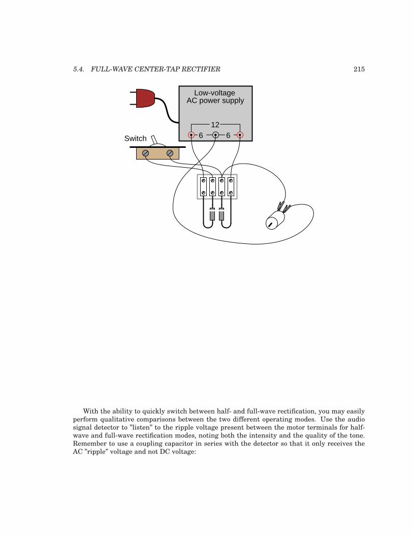
5.4. FULL-WAVE CENTER-TAP RECTIFIER 215
Low-voltage AC power supply
6 612
Switch
With the ability to quickly switch between half- and full-wave rectification, you may easilyperform qualitative comparisons between the two different operating modes. Use the audiosignal detector to ”listen” to the ripple voltage present between the motor terminals for half-wave and full-wave rectification modes, noting both the intensity and the quality of the tone.Remember to use a coupling capacitor in series with the detector so that it only receives theAC ”ripple” voltage and not DC voltage:

216 CHAPTER 5. DISCRETE SEMICONDUCTOR CIRCUITS
plug
headphones
Sensitivity
Capacitor0.1 µF
Test"probes"
COMPUTER SIMULATION
Schematic with SPICE node numbers:
V1
D11 2
0 0
3
2
2D2
V2
Rload
Netlist (make a text file containing the following text, verbatim):Fullwave center-tap rectifierv1 1 0 sin(0 8.485 60 0 0)v2 0 3 sin(0 8.485 60 0 0)rload 2 0 10kd1 1 2 mod1

5.4. FULL-WAVE CENTER-TAP RECTIFIER 217
d2 3 2 mod1.model mod1 d.tran .5m 25m.plot tran v(1,0) v(2,0).end

218 CHAPTER 5. DISCRETE SEMICONDUCTOR CIRCUITS
5.5 Full-wave bridge rectifier
PARTS AND MATERIALS
• Low-voltage AC power supply (6 volt output)
• Four 1N4001 rectifying diodes (Radio Shack catalog # 276-1101)
• Small ”hobby” motor, permanent-magnet type (Radio Shack catalog # 273-223 or equiva-lent)
CROSS-REFERENCES
Lessons In Electric Circuits, Volume 3, chapter 3: ”Diodes and Rectifiers”
LEARNING OBJECTIVES
• Design of a bridge rectifier circuit
• Advantages and disadvantages of the bridge rectifier circuit, compared to the center-tapcircuit
SCHEMATIC DIAGRAM
Mtr (motor)
ACpowersupply
ILLUSTRATION

5.5. FULL-WAVE BRIDGE RECTIFIER 219
Low-voltage AC power supply
6 612
Motor
Terminalstrip
INSTRUCTIONS
This circuit provides full-wave rectification without the necessity of a center-tapped trans-former. In applications where a center-tapped, or split-phase, source is unavailable, this is theonly practical method of full-wave rectification.
In addition to requiring more diodes than the center-tap circuit, the full-wave bridge suf-fers a slight performance disadvantage as well: the additional voltage drop caused by currenthaving to go through two diodes in each half-cycle rather than through only one. With a low-voltage source such as the one you’re using (6 volts RMS), this disadvantage is easily measured.Compare the DC voltage reading across the motor terminals with the reading obtained fromthe last experiment, given the same AC power supply and the same motor.
COMPUTER SIMULATION
Schematic with SPICE node numbers:
1
0
V1
1
0
23
D1 D2
D3 D4Rload
2
3
Netlist (make a text file containing the following text, verbatim):Fullwave bridge rectifierv1 1 0 sin(0 8.485 60 0 0)

220 CHAPTER 5. DISCRETE SEMICONDUCTOR CIRCUITS
rload 2 3 10kd1 3 1 mod1d2 1 2 mod1d3 3 0 mod1d4 0 2 mod1.model mod1 d.tran .5m 25m.plot tran v(1,0) v(2,3).end

5.6. RECTIFIER/FILTER CIRCUIT 221
5.6 Rectifier/filter circuit
PARTS AND MATERIALS
• Low-voltage AC power supply
• Bridge rectifier pack (Radio Shack catalog # 276-1185 or equivalent)
• Electrolytic capacitor, 1000 µF, at least 25 WVDC (Radio Shack catalog # 272-1047 orequivalent)
• Four ”banana” jack style binding posts, or other terminal hardware, for connection topotentiometer circuit (Radio Shack catalog # 274-662 or equivalent)
• Metal box
• 12-volt light bulb, 25 watt
• Lamp socket
A bridge rectifier ”pack” is highly recommended over constructing a bridge rectifier circuitfrom individual diodes, because such ”packs” are made to bolt onto a metal heat sink. A metalbox is recommended over a plastic box for its ability to function as a heat sink for the rectifier.
A larger capacitor value is fine to use in this experiment, so long as its working voltage ishigh enough. To be safe, choose a capacitor with a working voltage rating at least twice theRMS AC voltage output of the low-voltage AC power supply.
High-wattage 12-volt lamps may be purchased from recreational vehicle (RV) and boatingsupply stores. Common sizes are 25 watt and 50 watt. This lamp will be used as a ”heavy” loadfor the power supply.
CROSS-REFERENCES
Lessons In Electric Circuits, Volume 2, chapter 8: ”Filters”
LEARNING OBJECTIVES
• Capacitive filter function in an AC/DC power supply
• Importance of heat sinks for power semiconductors
SCHEMATIC DIAGRAM
AC
Rectifier
- +in
DCout

222 CHAPTER 5. DISCRETE SEMICONDUCTOR CIRCUITS
ILLUSTRATION
+
-
AC
AC--AC
inDCout
Rectifier Capacitor
INSTRUCTIONS
This experiment involves constructing a rectifier and filter circuit for attachment to thelow-voltage AC power supply constructed earlier. With this device, you will have a source oflow-voltage, DC power suitable as a replacement for a battery in battery-powered experiments.If you would like to make this device its own, self-contained 120VAC/DC power supply, youmay add all the componentry of the low-voltage AC supply to the ”AC in” side of this circuit:a transformer, power cord, and plug. Even if you don’t choose to do this, I recommend using ametal box larger than necessary to provide room for additional voltage regulation circuitry youmight choose to add to this project later.
The bridge rectifier unit should be rated for a current at least as high as the transformer’ssecondary winding is rated for, and for a voltage at least twice as high as the RMS voltage ofthe transformer’s output (this allows for peak voltage, plus an additional safety margin). TheRadio Shack rectifier specified in the parts list is rated for 25 amps and 50 volts, more thanenough for the output of the low-voltage AC power supply specified in the AC experimentschapter.
Rectifier units of this size are often equipped with ”quick-disconnect” terminals. Comple-mentary ”quick-disconnect” lugs are sold that crimp onto the bare ends of wire. This is thepreferred method of terminal connection. You may solder wires directly to the lugs of the recti-fier, but I recommend against direct soldering to any semiconductor component for two reasons:possible heat damage during soldering, and difficulty of replacing the component in the eventof failure.
Semiconductor devices are more prone to failure than most of the components covered inthese experiments thus far, and so if you have any intent of making a circuit permanent, youshould build it to be maintained. ”Maintainable construction” involves, among other things,making all delicate components replaceable. It also means making ”test points” accessible tometer probes throughout the circuit, so that troubleshooting may be executed with a mini-

5.6. RECTIFIER/FILTER CIRCUIT 223
mum of inconvenience. Terminal strips inherently provide test points for taking voltage mea-surements, and they also allow for easy disconnection of wires without sacrificing connectiondurability.
Bolt the rectifier unit to the inside of the metal box. The box’s surface area will act as aradiator, keeping the rectifier unit cool as it passes high currents. Any metal radiator surfacedesigned to lower the operating temperature of an electronic component is called a heat sink.Semiconductor devices in general are prone to damage from overheating, so providing a pathfor heat transfer from the device(s) to the ambient air is very important when the circuit inquestion may handle large amounts of power.
A capacitor is included in the circuit to act as a filter to reduce ripple voltage. Make sure thatyou connect the capacitor properly across the DC output terminals of the rectifier, so that thepolarities match. Being an electrolytic capacitor, it is sensitive to damage by polarity reversal.In this circuit especially, where the internal resistance of the transformer and rectifier are lowand the short-circuit current consequently is high, the potential for damage is great. Warning:
a failed capacitor in this circuit will likely explode with alarming force!
After the rectifier/filter circuit is built, connect it to the low-voltage AC power supply likethis:
+
-
AC
AC--AC
inDCout
Rectifier Capacitor
Low-voltage AC power supply
6 612
Measure the AC voltage output by the low-voltage power supply. Your meter should indicateapproximately 6 volts if the circuit is connected as shown. This voltage measurement is theRMS voltage of the AC power supply.
Now, switch your multimeter to the DC voltage function and measure the DC voltage outputby the rectifier/filter circuit. It should read substantially higher than the RMS voltage of theAC input measured before. The filtering action of the capacitor provides a DC output voltageequal to the peak AC voltage, hence the greater voltage indication:

224 CHAPTER 5. DISCRETE SEMICONDUCTOR CIRCUITS
Time
Full-wave, rectified DC voltage
Time
Full-wave, rectified DC voltage, with filtering
Measure the AC ripple voltage magnitude with a digital voltmeter set to AC volts (or ACmillivolts). You should notice a much smaller ripple voltage in this circuit than what wasmeasured in any of the unfiltered rectifier circuits previously built. Feel free to use your audiodetector to ”listen” to the AC ripple voltage output by the rectifier/filter unit. As usual, connecta small ”coupling” capacitor in series with the detector so that it does not respond to the DCvoltage, but only the AC ripple. Very little sound should be heard.
After taking unloaded AC ripple voltage measurements, connect the 25 watt light bulb tothe output of the rectifier/filter circuit like this:
+
-
AC
AC--AC
inDCout
Rectifier Capacitor
Low-voltage AC power supply
6 612
Re-measure the ripple voltage present between the rectifier/filter unit’s ”DC out” terminals.With a heavy load, the filter capacitor becomes discharged between rectified voltage peaks,resulting in greater ripple than before:

5.6. RECTIFIER/FILTER CIRCUIT 225
Time
Full-wave, filtered DC voltage under heavy load
If less ripple is desired under heavy-load conditions, a larger capacitor may be used, or amore complex filter circuit may be built using two capacitors and an inductor:
DCout
If you choose to build such a filter circuit, be sure to use an iron-core inductor for maximuminductance, and one with thick enough wire to safely handle the full rated current of powersupply. Inductors used for the purpose of filtering are sometimes referred to as chokes, becausethey ”choke” AC ripple voltage from getting to the load. If a suitable choke cannot be obtained,the secondary winding of a step-down power transformer like the type used to step 120 voltsAC down to 12 or 6 volts AC in the low-voltage power supply may be used. Leave the primary(120 volt) winding open:
DCout
Leave these wiresdisconnected!
COMPUTER SIMULATION
Schematic with SPICE node numbers:

226 CHAPTER 5. DISCRETE SEMICONDUCTOR CIRCUITS
1
0
V1
1
0
23
D1 D2
D3 D4Rload
2
3
C1
Netlist (make a text file containing the following text, verbatim):Fullwave bridge rectifierv1 1 0 sin(0 8.485 60 0 0)rload 2 3 10kc1 2 3 1000u ic=0d1 3 1 mod1d2 1 2 mod1d3 3 0 mod1d4 0 2 mod1.model mod1 d.tran .5m 25m.plot tran v(1,0) v(2,3).end
You may decrease the value of Rload in the simulation from 10 kΩ to some lower value toexplore the effects of loading on ripple voltage. As it is with a 10 kΩ load resistor, the ripple isundetectable on the waveform plotted by SPICE.

5.7. VOLTAGE REGULATOR 227
5.7 Voltage regulator
PARTS AND MATERIALS
• Four 6 volt batteries
• Zener diode, 12 volt – type 1N4742 (Radio Shack catalog # 276-563 or equivalent)
• One 10 kΩ resistor
Any low-voltage zener diode is appropriate for this experiment. The 1N4742 model listedhere (zener voltage = 12 volts) is but one suggestion. Whatever diode model you choose, Ihighly recommend one with a zener voltage rating greater than the voltage of a single battery,for maximum learning experience. It is important that you see how a zener diode functionswhen exposed to a voltage less than its breakdown rating.
CROSS-REFERENCES
Lessons In Electric Circuits, Volume 3, chapter 3: ”Diodes and Rectifiers”
LEARNING OBJECTIVES
• Zener diode function
SCHEMATIC DIAGRAM
10 kΩ
Zenerdiode
ILLUSTRATION
+-

228 CHAPTER 5. DISCRETE SEMICONDUCTOR CIRCUITS
INSTRUCTIONS
Build this simple circuit, being sure to connect the diode in ”reverse-bias” fashion (cathodepositive and anode negative), and measure the voltage across the diode with one battery asa power source. Record this voltage drop for future reference. Also, measure and record thevoltage drop across the 10 kΩ resistor.
Modify the circuit by connecting two 6-volt batteries in series, for 12 volts total power sourcevoltage. Re-measure the diode’s voltage drop, as well as the resistor’s voltage drop, with avoltmeter:
+-
+-
COMA
V
V A
AOFF
Connect three, then four 6-volt batteries together in series, forming an 18 volt and 24 voltpower source, respectively. Measure and record the diode’s and resistor’s voltage drops foreach new power supply voltage. What do you notice about the diode’s voltage drop for thesefour different source voltages? Do you see how the diode voltage never exceeds a level of 12volts? What do you notice about the resistor’s voltage drop for these four different sourcevoltage levels?
Zener diodes are frequently used as voltage regulating devices, because they act to clampthe voltage drop across themselves at a predetermined level. Whatever excess voltage is sup-plied by the power source becomes dropped across the series resistor. However, it is importantto note that a zener diode cannot make up for a deficiency in source voltage. For instance, this12-volt zener diode does not drop 12 volts when the power source is only 6 volts strong. It ishelpful to think of a zener diode as a voltage limiter: establishing a maximum voltage drop,

5.7. VOLTAGE REGULATOR 229
but not a minimum voltage drop.
COMPUTER SIMULATION
Schematic with SPICE node numbers:
10 kΩ
Zenerdiode
1
0 0
2
Netlist (make a text file containing the following text, verbatim):Zener diodev1 1 0r1 1 2 10kd1 0 2 mod1.model mod1 d bv=12.dc v1 18 18 1.print dc v(2,0).end
A zener diode may be simulated in SPICE with a normal diode, the reverse breakdownparameter (bv=12 ) set to the desired zener breakdown voltage.

230 CHAPTER 5. DISCRETE SEMICONDUCTOR CIRCUITS
5.8 Transistor as a switch
PARTS AND MATERIALS
• Two 6-volt batteries
• One NPN transistor – models 2N2222 or 2N3403 recommended (Radio Shack catalog #276-1617 is a package of fifteen NPN transistors ideal for this and other experiments)
• One 100 kΩ resistor
• One 560 Ω resistor
• One light-emitting diode (Radio Shack catalog # 276-026 or equivalent)
Resistor values are not critical for this experiment. Neither is the particular light emittingdiode (LED) selected.
CROSS-REFERENCES
Lessons In Electric Circuits, Volume 3, chapter 4: ”Bipolar Junction Transistors”
LEARNING OBJECTIVES
• Current amplification of a bipolar junction transistor
SCHEMATIC DIAGRAM
Q1
6 V
6 V 100 kΩ
560 Ω
ILLUSTRATION

5.8. TRANSISTOR AS A SWITCH 231
CBE
+-
+-
INSTRUCTIONS
The red wire shown in the diagram (the one terminating in an arrowhead, connected to oneend of the 100 kΩ resistor) is intended to remain loose, so that you may touch it momentarilyto other points in the circuit.
If you touch the end of the loose wire to any point in the circuit more positive than it, suchas the positive side of the DC power source, the LED should light up. It takes 20 mA to fullyilluminate a standard LED, so this behavior should strike you as interesting, because the 100kΩ resistor to which the loose wire is attached restricts current through it to a far lesser valuethan 20 mA. At most, a total voltage of 12 volts across a 100 kΩ resistance yields a current ofonly 0.12 mA, or 120 µA! The connection made by your touching the wire to a positive pointin the circuit conducts far less current than 1 mA, yet through the amplifying action of thetransistor, is able to control a much greater current through the LED.
Try using an ammeter to connect the loose wire to the positive side of the power source, likethis:

232 CHAPTER 5. DISCRETE SEMICONDUCTOR CIRCUITS
CBE
+-
+-
COMA
V
V A
AOFF
You may have to select the most sensitive current range on the meter to measure this smallflow. After measuring this controlling current, try measuring the LED’s current (the controlledcurrent) and compare magnitudes. Don’t be surprised if you find a ratio in excess of 200 (thecontrolled current 200 times as great as the controlling current)!
As you can see, the transistor is acting as a kind of electrically-controlled switch, switchingcurrent on and off to the LED at the command of a much smaller current signal conductedthrough its base terminal.
To further illustrate just how miniscule the controlling current is, remove the loose wirefrom the circuit and try ”bridging” the unconnected end of the 100 kΩ resistor to the powersource’s positive pole with two fingers of one hand. You may need to wet the ends of thosefingers to maximize conductivity:
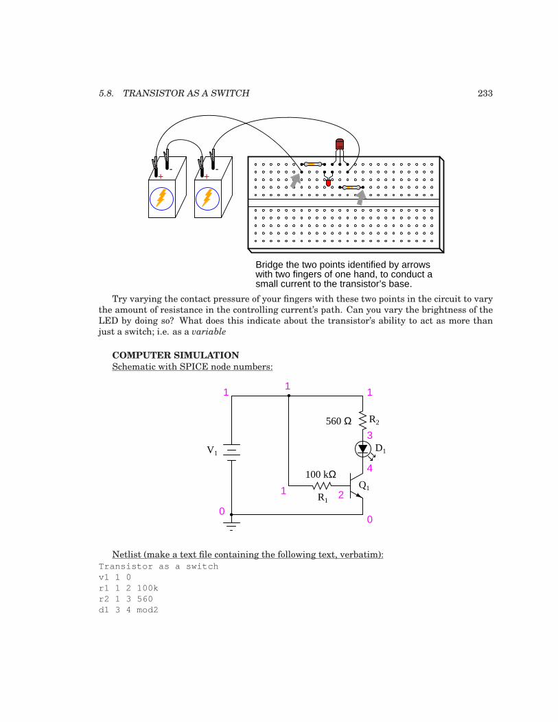
5.8. TRANSISTOR AS A SWITCH 233
CBE
+-
+-
Bridge the two points identified by arrowswith two fingers of one hand, to conduct asmall current to the transistor’s base.
Try varying the contact pressure of your fingers with these two points in the circuit to varythe amount of resistance in the controlling current’s path. Can you vary the brightness of theLED by doing so? What does this indicate about the transistor’s ability to act as more thanjust a switch; i.e. as a variable
COMPUTER SIMULATION
Schematic with SPICE node numbers:
Q1
100 kΩ
560 Ω
V1
1
00
11
1 2
3
4
R1
R2
D1
Netlist (make a text file containing the following text, verbatim):Transistor as a switchv1 1 0r1 1 2 100kr2 1 3 560d1 3 4 mod2

234 CHAPTER 5. DISCRETE SEMICONDUCTOR CIRCUITS
q1 4 2 0 mod1.model mod1 npn bf=200.model mod2 d is=1e-28.dc v1 12 12 1.print dc v(2,0) v(4,0) v(1,2) v(1,3) v(3,4).end
In this simulation, the voltage drop across the 560 Ω resistor v(1,3) turns out to be 10.26volts, indicating a LED current of 18.32 mA by Ohm’s Law (I=E/R). R1’s voltage drop (voltagebetween nodes 1 and 2) ends up being 11.15 volts, which across 100 kΩ gives a current of only111.5 µA. Obviously, a very small current is exerting control over a much larger current in thiscircuit.
In case you were wondering, the is=1e-28 parameter in the diode’s .model line is thereto make the diode act more like an LED with a higher forward voltage drop.

5.9. STATIC ELECTRICITY SENSOR 235
5.9 Static electricity sensor
PARTS AND MATERIALS
• One N-channel junction field-effect transistor, models 2N3819 or J309 recommended (Ra-dio Shack catalog # 276-2035 is the model 2N3819)
• One 6 volt battery
• One 100 kΩ resistor
• One light-emitting diode (Radio Shack catalog # 276-026 or equivalent)
• Plastic comb
The particular junction field-effect transistor, or JFET, model used in this experiment is notcritical. P-channel JFETs are also okay to use, but are not as popular as N-channel transistors.
Beware that not all transistors share the same terminal designations, or pinouts, even ifthey share the same physical appearance. This will dictate how you connect the transistorstogether and to other components, so be sure to check the manufacturer’s specifications (com-ponent datasheet), easily obtained from the manufacturer’s website. Beware that it is possiblefor the transistor’s package and even the manufacturer’s datasheet to show incorrect terminalidentification diagrams! Double-checking pin identities with your multimeter’s ”diode check”function is highly recommended. For details on how to identify junction field-effect transistorterminals using a multimeter, consult chapter 5 of the Semiconductor volume (volume III) ofthis book series.
CROSS-REFERENCES
Lessons In Electric Circuits, Volume 3, chapter 5: ”Junction Field-Effect Transistors”
LEARNING OBJECTIVES
• How the JFET is used as an on/off switch
• How JFET current gain differs from a bipolar transistor
SCHEMATIC DIAGRAM
Q1
6 V 100 kΩ

236 CHAPTER 5. DISCRETE SEMICONDUCTOR CIRCUITS
ILLUSTRATION
+-
SGD
INSTRUCTIONS
This experiment is very similar to the previous experiment using a bipolar junction tran-sistor (BJT) as a switching device to control current through an LED. In this experiment, ajunction field-effect transistor is used instead, giving dramatically improved sensitivity.
Build this circuit and touch the loose wire end (the wire shown in red on the schematicdiagram and in the illustration, connected to the 100 kΩ resistor) with your hand. Simplytouching this wire will likely have an effect on the LED’s status. This circuit makes a finesensor of static electricity! Try scuffing your feet on a carpet and then touching the wire end ifno effect on the light is seen yet.
For a more controlled test, touch the wire with one hand and alternately touch the positive(+) and negative (-) terminals of the battery with one finger of your other hand. Your body actsas a conductor (albeit a poor one), connecting the gate terminal of the JFET to either terminalof the battery as you touch them. Make note which terminal makes the LED turn on andwhich makes the LED turn off. Try to relate this behavior with what you’ve read about JFETsin chapter 5 of the Semiconductor volume.
The fact that a JFET is turned on and off so easily (requiring so little control current), asevidenced by full on-and-off control simply by conduction of a control current through yourbody, demonstrates how great of a current gain it has. With the BJT ”switch” experiment, amuch more ”solid” connection between the transistor’s gate terminal and a source of voltagewas needed to turn it on. Not so with the JFET. In fact, the mere presence of static electricitycan turn it on and off at a distance.
To further experiment with the effects of static electricity on this circuit, brush your hairwith the plastic comb and then wave the comb near the transistor, watching the effect on theLED. The action of combing your hair with a plastic object creates a high static voltage betweenthe comb and your body. The strong electric field produced between these two objects shouldbe detectable by this circuit from a significant distance!
In case you’re wondering why there is no 560 Ω ”dropping” resistor to limit current throughthe LED, many small-signal JFETs tend to self-limit their controlled current to a level accept-able by LEDs. The model 2N3819, for example, has a typical saturated drain current (IDSS) of

5.9. STATIC ELECTRICITY SENSOR 237
10 mA and a maximum of 20 mA. Since most LEDs are rated at a forward current of 20 mA,there is no need for a dropping resistor to limit circuit current: the JFET does it intrinsically.

238 CHAPTER 5. DISCRETE SEMICONDUCTOR CIRCUITS
5.10 Pulsed-light sensor
PARTS AND MATERIALS
• Two 6-volt batteries
• One NPN transistor – models 2N2222 or 2N3403 recommended (Radio Shack catalog #276-1617 is a package of fifteen NPN transistors ideal for this and other experiments)
• One light-emitting diode (Radio Shack catalog # 276-026 or equivalent)
• Audio detector with headphones
If you don’t have an audio detector already constructed, you can use a nice set of audio head-phones (closed-cup style, that completely covers your ears) and a 120V/6V step-down trans-former to build a sensitive audio detector without volume control or overvoltage protection,just for this experiment.
Connect these portions of the headphone stereo plug to the transformer’s secondary (6 volt)winding:
common right left common right left
Speakers in series Speakers in parallel
To transformer To transformer
Try both the series and the parallel connection schemes for the loudest sound.If you haven’t made an audio detector as outlined in both the DC and AC experiments
chapters, you really should – it is a valuable piece of test equipment for your collection.
CROSS-REFERENCES
Lessons In Electric Circuits, Volume 3, chapter 4: ”Bipolar Junction Transistors”
LEARNING OBJECTIVES
• How to use a transistor as a crude common-emitter amplifier
• How to use an LED as a light sensor
SCHEMATIC DIAGRAM

5.10. PULSED-LIGHT SENSOR 239
6 V
ILLUSTRATION
plug
headphones
Sensitivity
+-
CBE
INSTRUCTIONS
This circuit detects pulses of light striking the LED and converts them into relatively strongaudio signals to be heard through the headphones. Forrest Mims teaches that LEDs have the

240 CHAPTER 5. DISCRETE SEMICONDUCTOR CIRCUITS
ability to produce current when exposed to light, in a manner not unlike a semiconductor solarcell. [1] By itself, the LED does not produce enough electrical power to drive the audio detectorcircuit, so a transistor is used to amplify the LED’s signals. If the LED is exposed to a pulsingsource of light, a tone will be heard in the headphones.
Sources of light suitable for this experiment include fluorescent and neon lamps, whichblink rapidly with the 60 Hz AC power energizing them. You may also try using bright sunlightfor a steady light source, then waving your fingers in front of the LED. The rapidly passingshadows will cause the LED to generate pulses of voltage, creating a brief ”buzzing” sound inthe headphones.
LEDs serving as photo-detectors are narrow-band devices, responding to a narrow bandof wavelengths close, but not identical, to that normally emitted. Infrared remote controlsare a good illumination source for near-infrared LEDs employed as photo-sensors, producing areceiver sound. [3]
With a little imagination, it is not difficult to grasp the concept of transmitting audio infor-mation – such as music or speech – over a beam of pulsing light. Given a suitable ”transmitter”circuit to pulse an LED on and off with the positive and negative crests of an audio waveformfrom a microphone, the ”receiver” circuit shown here would convert those light pulses back intoaudio signals. [2]

5.11. VOLTAGE FOLLOWER 241
5.11 Voltage follower
PARTS AND MATERIALS
• One NPN transistor – models 2N2222 or 2N3403 recommended (Radio Shack catalog #276-1617 is a package of fifteen NPN transistors ideal for this and other experiments)
• Two 6-volt batteries
• Two 1 kΩ resistors
• One 10 kΩ potentiometer, single-turn, linear taper (Radio Shack catalog # 271-1715)
Beware that not all transistors share the same terminal designations, or pinouts, even ifthey share the same physical appearance. This will dictate how you connect the transistorstogether and to other components, so be sure to check the manufacturer’s specifications (com-ponent datasheet), easily obtained from the manufacturer’s website. Beware that it is possiblefor the transistor’s package and even the manufacturer’s datasheet to show incorrect terminalidentification diagrams! Double-checking pin identities with your multimeter’s ”diode check”function is highly recommended. For details on how to identify bipolar transistor terminalsusing a multimeter, consult chapter 4 of the Semiconductor volume (volume III) of this bookseries.
CROSS-REFERENCES
Lessons In Electric Circuits, Volume 3, chapter 4: ”Bipolar Junction Transistors”
LEARNING OBJECTIVES
• Purpose of circuit ”ground” when there is no actual connection to earth ground
• Using a shunt resistor to measure current with a voltmeter
• Measure amplifier voltage gain
• Measure amplifier current gain
• Amplifier impedance transformation
SCHEMATIC DIAGRAM
Q1
Rbase
Rload
10 kΩ
6 V
6 V1 kΩ
1 kΩ

242 CHAPTER 5. DISCRETE SEMICONDUCTOR CIRCUITS
ILLUSTRATION
CBE
+-
+-
INSTRUCTIONS
Again, beware that the transistor you select for this experiment may not have the sameterminal designations shown here, and so the breadboard layout shown in the illustration maynot be correct for you. In my illustrations, I show all TO-92 package transistors with terminalslabeled ”CBE”: Collector, Base, and Emitter, from left to right. This is correct for the model2N2222 transistor and some others, but not for all; not even for all NPN-type transistors! Asusual, check with the manufacturer for details on the particular component(s) you choose fora project. With bipolar junction transistors, it is easy enough to verify terminal assignmentswith a multimeter.
The voltage follower is the safest and easiest transistor amplifier circuit to build. Its pur-pose is to provide approximately the same voltage to a load as what is input to the amplifier,but at a much greater current. In other words, it has no voltage gain, but it does have currentgain.
Note that the negative (-) side of the power supply is shown in the schematic diagram to beconnected to ground, as indicated by the symbol in the lower-left corner of the diagram. Thisdoes not necessarily represent a connection to the actual earth. What it means is that thispoint in the circuit – and all points electrically common to it – constitute the default referencepoint for all voltage measurements in the circuit. Since voltage is by necessity a quantityrelative between two points, a ”common” point of reference designated in a circuit gives us theability to speak meaningfully of voltage at particular, single points in that circuit.

5.11. VOLTAGE FOLLOWER 243
Q1
Rbase
Rload
10 kΩ
6 V
6 V
These pointsare all considered "ground"
1 kΩ
1 kΩ
For example, if I were to speak of voltage at the base of the transistor (VB), I would meanthe voltage measured between the transistor’s base terminal and the negative side of the powersupply (ground), with the red probe touching the base terminal and the black probe touchingground. Normally, it is nonsense to speak of voltage at a single point, but having an implicitreference point for voltage measurements makes such statements meaningful:
Q1
Rbase
Rload
10 kΩ
6 V
6 V
+V
-Voltmeter measuring
base voltage (VB)
1 kΩ
1 kΩ
Build this circuit, and measure output voltage versus input voltage for several differentpotentiometer settings. Input voltage is the voltage at the potentiometer’s wiper (voltage be-tween the wiper and circuit ground), while output voltage is the load resistor voltage (voltageacross the load resistor, or emitter voltage: between emitter and circuit ground). You shouldsee a close correlation between these two voltages: one is just a little bit greater than the other(about 0.6 volts or so?), but a change in the input voltage gives almost equal change in theoutput voltage. Because the relationship between input change and output change is almost1:1, we say that the AC voltage gain of this amplifier is nearly 1.
Not very impressive, is it? Now measure current through the base of the transistor (inputcurrent) versus current through the load resistor (output current). Before you break the cir-cuit and insert your ammeter to take these measurements, consider an alternative method:measure voltage across the base and load resistors, whose resistance values are known. UsingOhm’s Law, current through each resistor may be easily calculated: divide the measured volt-

244 CHAPTER 5. DISCRETE SEMICONDUCTOR CIRCUITS
age by the known resistance (I=E/R). This calculation is particularly easy with resistors of 1 kΩ
value: there will be 1 milliamp of current for every volt of drop across them. For best precision,you may measure the resistance of each resistor rather than assume an exact value of 1 kΩ,but it really doesn’t matter much for the purposes of this experiment. When resistors are usedto take current measurements by ”translating” a current into a corresponding voltage, they areoften referred to as shunt resistors.
You should expect to find huge differences between input and output currents for this am-plifier circuit. In fact, it is not uncommon to experience current gains well in excess of 200for a small-signal transistor operating at low current levels. This is the primary purpose of avoltage follower circuit: to boost the current capacity of a ”weak” signal without altering itsvoltage.
Another way of thinking of this circuit’s function is in terms of impedance. The input side ofthis amplifier accepts a voltage signal without drawing much current. The output side of thisamplifier delivers the same voltage, but at a current limited only by load resistance and thecurrent-handling ability of the transistor. Cast in terms of impedance, we could say that thisamplifier has a high input impedance (voltage dropped with very little current drawn) and alow output impedance (voltage dropped with almost unlimited current-sourcing capacity).
COMPUTER SIMULATION
Schematic with SPICE node numbers:
Q1
Rbase
Rload
1 kΩ
1 kΩ
V1
Rpot1
Rpot2
5 kΩ
5 kΩ
1
00 0
1 1
23
4
Netlist (make a text file containing the following text, verbatim):Voltage followerv1 1 0rpot1 1 2 5krpot2 2 0 5krbase 2 3 1krload 4 0 1kq1 1 3 4 mod1.model mod1 npn bf=200.dc v1 12 12 1.print dc v(2,0) v(4,0) v(2,3).end

5.11. VOLTAGE FOLLOWER 245
When this simulation is run through the SPICE program, it shows an input voltage of 5.937volts and an output voltage of 5.095 volts, with an input current of 25.35 µA (2.535E-02 voltsdropped across the 1 kΩ Rbase resistor). Output current is, of course, 5.095 mA, inferred fromthe output voltage of 5.095 volts dropped across a load resistance of exactly 1 kΩ. You maychange the ”potentiometer” setting in this circuit by adjusting the values of Rpot1 and Rpot2,always keeping their sum at 10 kΩ.

246 CHAPTER 5. DISCRETE SEMICONDUCTOR CIRCUITS
5.12 Common-emitter amplifier
PARTS AND MATERIALS
• One NPN transistor – model 2N2222 or 2N3403 recommended (Radio Shack catalog #276-1617 is a package of fifteen NPN transistors ideal for this and other experiments)
• Two 6-volt batteries
• One 10 kΩ potentiometer, single-turn, linear taper (Radio Shack catalog # 271-1715)
• One 1 MΩ resistor
• One 100 kΩ resistor
• One 10 kΩ resistor
• One 1.5 kΩ resistor
CROSS-REFERENCES
Lessons In Electric Circuits, Volume 3, chapter 4: ”Bipolar Junction Transistors”
LEARNING OBJECTIVES
• Design of a simple common-emitter amplifier circuit
• How to measure amplifier voltage gain
• The difference between an inverting and a noninverting amplifier
• Ways to introduce negative feedback in an amplifier circuit
SCHEMATIC DIAGRAM
10 kΩ100 kΩ
Q1
10 kΩ
6 V
6 V
Vout
Vin
ILLUSTRATION
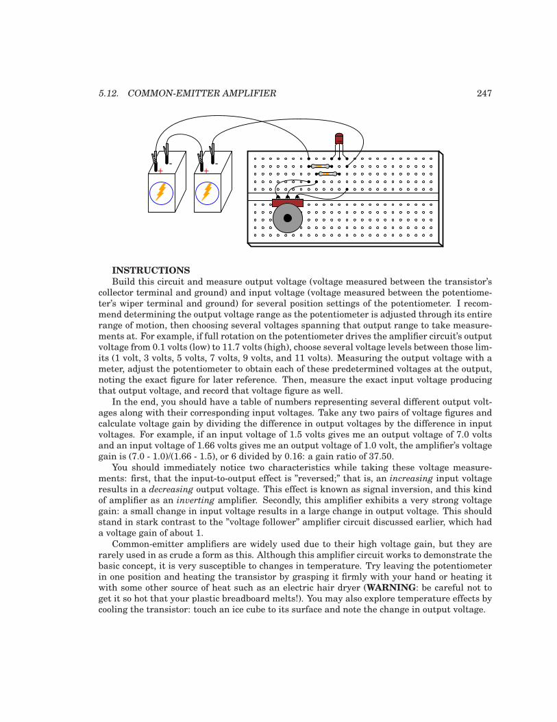
5.12. COMMON-EMITTER AMPLIFIER 247
CBE
+-
+-
INSTRUCTIONS
Build this circuit and measure output voltage (voltage measured between the transistor’scollector terminal and ground) and input voltage (voltage measured between the potentiome-ter’s wiper terminal and ground) for several position settings of the potentiometer. I recom-mend determining the output voltage range as the potentiometer is adjusted through its entirerange of motion, then choosing several voltages spanning that output range to take measure-ments at. For example, if full rotation on the potentiometer drives the amplifier circuit’s outputvoltage from 0.1 volts (low) to 11.7 volts (high), choose several voltage levels between those lim-its (1 volt, 3 volts, 5 volts, 7 volts, 9 volts, and 11 volts). Measuring the output voltage with ameter, adjust the potentiometer to obtain each of these predetermined voltages at the output,noting the exact figure for later reference. Then, measure the exact input voltage producingthat output voltage, and record that voltage figure as well.
In the end, you should have a table of numbers representing several different output volt-ages along with their corresponding input voltages. Take any two pairs of voltage figures andcalculate voltage gain by dividing the difference in output voltages by the difference in inputvoltages. For example, if an input voltage of 1.5 volts gives me an output voltage of 7.0 voltsand an input voltage of 1.66 volts gives me an output voltage of 1.0 volt, the amplifier’s voltagegain is (7.0 - 1.0)/(1.66 - 1.5), or 6 divided by 0.16: a gain ratio of 37.50.
You should immediately notice two characteristics while taking these voltage measure-ments: first, that the input-to-output effect is ”reversed;” that is, an increasing input voltageresults in a decreasing output voltage. This effect is known as signal inversion, and this kindof amplifier as an inverting amplifier. Secondly, this amplifier exhibits a very strong voltagegain: a small change in input voltage results in a large change in output voltage. This shouldstand in stark contrast to the ”voltage follower” amplifier circuit discussed earlier, which hada voltage gain of about 1.
Common-emitter amplifiers are widely used due to their high voltage gain, but they arerarely used in as crude a form as this. Although this amplifier circuit works to demonstrate thebasic concept, it is very susceptible to changes in temperature. Try leaving the potentiometerin one position and heating the transistor by grasping it firmly with your hand or heating itwith some other source of heat such as an electric hair dryer (WARNING: be careful not toget it so hot that your plastic breadboard melts!). You may also explore temperature effects bycooling the transistor: touch an ice cube to its surface and note the change in output voltage.

248 CHAPTER 5. DISCRETE SEMICONDUCTOR CIRCUITS
When the transistor’s temperature changes, its base-emitter diode characteristics change,resulting in different amounts of base current for the same input voltage. This in turn al-ters the controlled current through the collector terminal, thus affecting output voltage. Suchchanges may be minimized through the use of signal feedback, whereby a portion of the outputvoltage is ”fed back” to the amplifier’s input so as to have a negative, or canceling, effect onvoltage gain. Stability is improved at the expense of voltage gain, a compromise solution, butpractical nonetheless.
Perhaps the simplest way to add negative feedback to a common-emitter amplifier is to addsome resistance between the emitter terminal and ground, so that the input voltage becomesdivided between the base-emitter PN junction and the voltage drop across the new resistance:
10 kΩ100 kΩ
Q1
10 kΩ
6 V
6 V
Vout
Vin
1.5 kΩ
CBE
+-
+-
Repeat the same voltage measurement and recording exercise with the 1.5 kΩ resistor in-stalled, calculating the new (reduced) voltage gain. Try altering the transistor’s temperatureagain and noting the output voltage for a steady input voltage. Does it change more or lessthan without the 1.5 kΩ resistor?
Another method of introducing negative feedback to this amplifier circuit is to ”couple” theoutput to the input through a high-value resistor. Connecting a 1 MΩ resistor between thetransistor’s collector and base terminals works well:

5.12. COMMON-EMITTER AMPLIFIER 249
10 kΩ100 kΩ
Q1
10 kΩ
6 V
6 V
Vout
Vin
1 MΩ
CBE
+-
+-
Although this different method of feedback accomplishes the same goal of increased stabil-ity by diminishing gain, the two feedback circuits will not behave identically. Note the range ofpossible output voltages with each feedback scheme (the low and high voltage values obtainedwith a full sweep of the input voltage potentiometer), and how this differs between the twocircuits.
COMPUTER SIMULATION
Schematic with SPICE node numbers:

250 CHAPTER 5. DISCRETE SEMICONDUCTOR CIRCUITS
100 kΩQ1
10 kΩ
Vout
Vin
Vsupply
1
0 0 0
1
2
34
Rc
Rb
Netlist (make a text file containing the following text, verbatim):Common-emitter amplifiervsupply 1 0 dc 12vin 3 0rc 1 2 10krb 3 4 100kq1 2 4 0 mod1.model mod1 npn bf=200.dc vin 0 2 0.05.plot dc v(2,0) v(3,0).end
This SPICE simulation sets up a circuit with a variable DC voltage source (vin ) as theinput signal, and measures the corresponding output voltage between nodes 2 and 0. Theinput voltage is varied, or ”swept,” from 0 to 2 volts in 0.05 volt increments. Results are shownon a plot, with the input voltage appearing as a straight line and the output voltage as a ”step”figure where the voltage begins and ends level, with a steep change in the middle where thetransistor is in its active mode of operation.
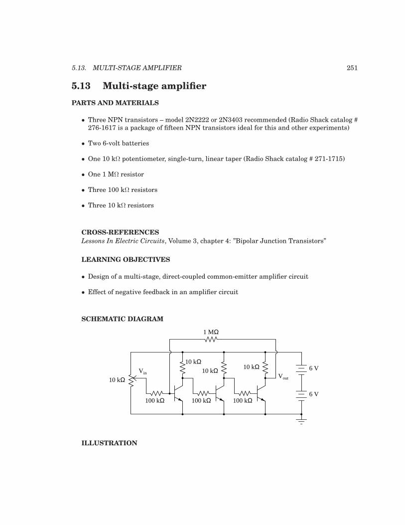
5.13. MULTI-STAGE AMPLIFIER 251
5.13 Multi-stage amplifier
PARTS AND MATERIALS
• Three NPN transistors – model 2N2222 or 2N3403 recommended (Radio Shack catalog #276-1617 is a package of fifteen NPN transistors ideal for this and other experiments)
• Two 6-volt batteries
• One 10 kΩ potentiometer, single-turn, linear taper (Radio Shack catalog # 271-1715)
• One 1 MΩ resistor
• Three 100 kΩ resistors
• Three 10 kΩ resistors
CROSS-REFERENCES
Lessons In Electric Circuits, Volume 3, chapter 4: ”Bipolar Junction Transistors”
LEARNING OBJECTIVES
• Design of a multi-stage, direct-coupled common-emitter amplifier circuit
• Effect of negative feedback in an amplifier circuit
SCHEMATIC DIAGRAM
Vout
100 kΩ
10 kΩ
100 kΩ
10 kΩ
100 kΩ
10 kΩ
10 kΩ
6 V
6 V
1 MΩ
Vin
ILLUSTRATION
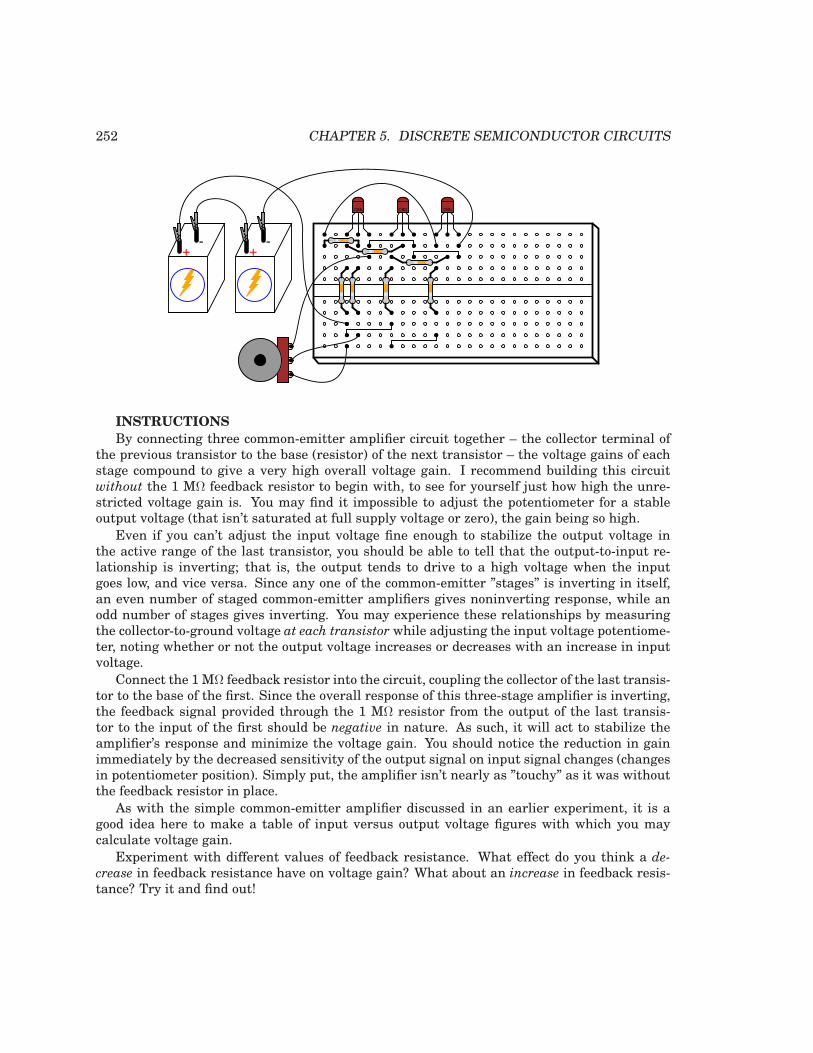
252 CHAPTER 5. DISCRETE SEMICONDUCTOR CIRCUITS
+-
+-
CBE CBE CBE
INSTRUCTIONS
By connecting three common-emitter amplifier circuit together – the collector terminal ofthe previous transistor to the base (resistor) of the next transistor – the voltage gains of eachstage compound to give a very high overall voltage gain. I recommend building this circuitwithout the 1 MΩ feedback resistor to begin with, to see for yourself just how high the unre-stricted voltage gain is. You may find it impossible to adjust the potentiometer for a stableoutput voltage (that isn’t saturated at full supply voltage or zero), the gain being so high.
Even if you can’t adjust the input voltage fine enough to stabilize the output voltage inthe active range of the last transistor, you should be able to tell that the output-to-input re-lationship is inverting; that is, the output tends to drive to a high voltage when the inputgoes low, and vice versa. Since any one of the common-emitter ”stages” is inverting in itself,an even number of staged common-emitter amplifiers gives noninverting response, while anodd number of stages gives inverting. You may experience these relationships by measuringthe collector-to-ground voltage at each transistor while adjusting the input voltage potentiome-ter, noting whether or not the output voltage increases or decreases with an increase in inputvoltage.
Connect the 1 MΩ feedback resistor into the circuit, coupling the collector of the last transis-tor to the base of the first. Since the overall response of this three-stage amplifier is inverting,the feedback signal provided through the 1 MΩ resistor from the output of the last transis-tor to the input of the first should be negative in nature. As such, it will act to stabilize theamplifier’s response and minimize the voltage gain. You should notice the reduction in gainimmediately by the decreased sensitivity of the output signal on input signal changes (changesin potentiometer position). Simply put, the amplifier isn’t nearly as ”touchy” as it was withoutthe feedback resistor in place.
As with the simple common-emitter amplifier discussed in an earlier experiment, it is agood idea here to make a table of input versus output voltage figures with which you maycalculate voltage gain.
Experiment with different values of feedback resistance. What effect do you think a de-
crease in feedback resistance have on voltage gain? What about an increase in feedback resis-tance? Try it and find out!

5.13. MULTI-STAGE AMPLIFIER 253
An advantage of using negative feedback to ”tame” a high-gain amplifier circuit is that theresulting voltage gain becomes more dependent upon the resistor values and less dependentupon the characteristics of the constituent transistors. This is good, because it is far easier tomanufacture consistent resistors than consistent transistors. Thus, it is easier to design anamplifier with predictable gain by building a staged network of transistors with an arbitrarilyhigh voltage gain, then mitigate that gain precisely through negative feedback. It is this sameprinciple that is used to make operational amplifier circuits behave so predictably.
This amplifier circuit is a bit simplified from what you will normally encounter in practicalmulti-stage circuits. Rarely is a pure common-emitter configuration (i.e. with no emitter-to-ground resistor) used, and if the amplifier’s service is for AC signals, the inter-stage couplingis often capacitive with voltage divider networks connected to each transistor base for properbiasing of each stage. Radio-frequency amplifier circuits are often transformer-coupled, withcapacitors connected in parallel with the transformer windings for resonant tuning.
COMPUTER SIMULATION
Schematic with SPICE node numbers:
Vout
100 kΩ
10 kΩ
100 kΩ
10 kΩ
100 kΩ
10 kΩ
1 MΩ
Vin
Vsupply
Q1 Q2 Q3
R1
R2
R3
R4
R5
R6
Rf 1
0000
0
111
2
34 5 6
63
7 8
Netlist (make a text file containing the following text, verbatim):Multi-stage amplifiervsupply 1 0 dc 12vin 2 0r1 2 3 100kr2 1 4 10kq1 4 3 0 mod1r3 4 7 100kr4 1 5 10kq2 5 7 0 mod1r5 5 8 100kr6 1 6 10kq3 6 8 0 mod1rf 3 6 1meg.model mod1 npn bf=200.dc vin 0 2.5 0.1

254 CHAPTER 5. DISCRETE SEMICONDUCTOR CIRCUITS
.plot dc v(6,0) v(2,0)
.end
This simulation plots output voltage against input voltage, and allows comparison betweenthose variables in numerical form: a list of voltage figures printed to the left of the plot. Youmay calculate voltage gain by taking any two analysis points and dividing the difference inoutput voltages by the difference in input voltages, just like you do for the real circuit.
Experiment with different feedback resistance values (rf ) and see the impact on overallvoltage gain. Do you notice a pattern? Here’s a hint: the overall voltage gain may be closelyapproximated by using the resistance figures of r1 and rf , without reference to any othercircuit component!
5.14. CURRENT MIRROR 255
5.14 Current mirror
PARTS AND MATERIALS
• Two NPN transistors – models 2N2222 or 2N3403 recommended (Radio Shack catalog #276-1617 is a package of fifteen NPN transistors ideal for this and other experiments)
• Two 6-volt batteries
• One 10 kΩ potentiometer, single-turn, linear taper (Radio Shack catalog # 271-1715)
• Two 10 kΩ resistors
• Four 1.5 kΩ resistors
Small signal transistors are recommended so as to be able to experience ”thermal runaway”in the latter portion of the experiment. Larger ”power” transistors may not exhibit the samebehavior at these low current levels. However, any pair of identical NPN transistors may beused to build a current mirror.
Beware that not all transistors share the same terminal designations, or pinouts, even ifthey share the same physical appearance. This will dictate how you connect the transistorstogether and to other components, so be sure to check the manufacturer’s specifications (com-ponent datasheet), easily obtained from the manufacturer’s website. Beware that it is possiblefor the transistor’s package and even the manufacturer’s datasheet to show incorrect terminalidentification diagrams! Double-checking pin identities with your multimeter’s ”diode check”function is highly recommended. For details on how to identify bipolar transistor terminalsusing a multimeter, consult chapter 4 of the Semiconductor volume (volume III) of this bookseries.
CROSS-REFERENCES
Lessons In Electric Circuits, Volume 3, chapter 4: ”Bipolar Junction Transistors”
LEARNING OBJECTIVES
• How to build a current mirror circuit
• Current limitations of a current mirror circuit
• Temperature dependence of BJTs
• Experience a controlled ”thermal runaway” situation
SCHEMATIC DIAGRAM

256 CHAPTER 5. DISCRETE SEMICONDUCTOR CIRCUITS
6 V
6 V
A+ -
Radjust
Rlimit Rload1
Rload2
Rload3
Rload4
TP1
TP2
TP3
TP4
TP5
Rload1 through Rload3
are 1.5 kΩ each
Rload4, Rlimit, and Radjust
are 10 kΩ each
Q1 Q2
ILLUSTRATION
CBE
+-
+-
COMA
V
V A
AOFF
TP5 TP4 TP3 TP2 TP1
CBE

5.14. CURRENT MIRROR 257
INSTRUCTIONS
A current mirror may be thought of as an adjustable current regulator, the current limitbeing easily set by a single resistance. It is a rather crude current regulator circuit, but onethat finds wide use due to its simplicity. In this experiment, you will get the opportunity tobuild one of these circuits, explore its current-regulating properties, and also experience someof its practical limitations firsthand.
Build the circuit as shown in the schematic and illustration. You will have one extra 1.5kΩ fixed-value resistor from the parts specified in the parts list. You will be using it in the lastpart of this experiment.
The potentiometer sets the amount of current through transistor Q1. This transistor isconnected to act as a simple diode: just a PN junction. Why use a transistor instead of a regulardiode? Because it is important to match the junction characteristics of these two transistorswhen using them in a current mirror circuit. Voltage dropped across the base-emitter junctionof Q1 is impressed across the base-emitter junction of the other transistor, Q2, causing it toturn ”on” and likewise conduct current.
Since voltage across the two transistors’ base-emitter junctions is the same – the two junc-tion pairs being connected in parallel with each other – so should the current be through theirbase terminals, assuming identical junction characteristics and identical junction tempera-tures. Matched transistors should have the same β ratios, as well, so equal base currentsmeans equal collector currents. The practical result of all this is Q2’s collector current mim-icking whatever current magnitude has been established through the collector of Q1 by thepotentiometer. In other words, current through Q2 mirrors the current through Q1.
Changes in load resistance (resistance connecting the collector of Q2 to the positive side ofthe battery) have no effect on Q1’s current, and consequently have no effect upon the base-emitter voltage or base current of Q2. With a constant base current and a nearly constant β
ratio, Q2 will drop as much or as little collector-emitter voltage as necessary to hold its collector(load) current constant. Thus, the current mirror circuit acts to regulate current at a value setby the potentiometer, without regard to load resistance.
Well, that is how it is supposed to work, anyway. Reality isn’t quite so simple, as you areabout to see. In the circuit diagram shown, the load circuit of Q2 is completed to the positiveside of the battery through an ammeter, for easy current measurement. Rather than solidlyconnect the ammeter’s black probe to a definite point in the circuit, I’ve marked five test points,TP1 through TP5, for you to touch the black test probe to while measuring current. This allowsyou to quickly and effortlessly change load resistance: touching the probe to TP1 results inpractically no load resistance, while touching it to TP5 results in approximately 14.5 kΩ ofload resistance.
To begin the experiment, touch the test probe to TP4 and adjust the potentiometer throughits range of travel. You should see a small, changing current indicated by your ammeter as youmove the potentiometer mechanism: no more than a few milliamps. Leave the potentiometerset to a position giving a round number of milliamps and move the meter’s black test probe toTP3. The current indication should be very nearly the same as before. Move the probe to TP2,then TP1. Again, you should see a nearly unchanged amount of current. Try adjusting thepotentiometer to another position, giving a different current indication, and touch the meter’sblack probe to test points TP1 through TP4, noting the stability of the current indications asyou change load resistance. This demonstrates the current regulating behavior of this circuit.

258 CHAPTER 5. DISCRETE SEMICONDUCTOR CIRCUITS
You should note that the current regulation isn’t perfect. Despite regulating the currentat nearly the value for load resistances between 0 and 4.5 kΩ, there is some variation overthis range. The regulation may be much worse if load resistance is allowed to rise too high.Try adjusting the potentiometer so that maximum current is obtained, as indicated with theammeter test probe connected to TP1. Leaving the potentiometer at that position, move themeter probe to TP2, then TP3, then TP4, and finally TP5, noting the meter’s indication at eachconnection point. The current should be regulated at a nearly constant value until the meterprobe is moved to the last test point, TP5. There, the current indication will be substantiallylower than at the other test points. Why is this? Because too much load resistance has beeninserted into Q2’s circuit. Simply put, Q2 cannot ”turn on” any more than it already has, tomaintain the same amount of current with this great a load resistance as with lesser loadresistances.
This phenomenon is common to all current-regulator circuits: there is a limited amountof resistance a current regulator can handle before it saturates. This stands to reason, asany current regulator circuit capable of supplying a constant amount of current through any
load resistance imaginable would require an unlimited source of voltage to do it! Ohm’s Law(E=IR) dictates the amount of voltage needed to push a given amount of current through agiven amount of resistance, and with only 12 volts of power supply voltage at our disposal, afinite limit of load current and load resistance definitely exists for this circuit. For this reason,it may be helpful to think of current regulator circuits as being current limiter circuits, for allthey can really do is limit current to some maximum value.
An important caveat for current mirror circuits in general is that of equal temperaturebetween the two transistors. The current ”mirroring” taking place between the two transistors’collector circuits depends on the base-emitter junctions of those two transistors having theexact same properties. As the ”diode equation” describes, the voltage/current relationship fora PN junction strongly depends on junction temperature. The hotter a PN junction is, themore current it will pass for a given amount of voltage drop. If one transistor should becomehotter than the other, it will pass more collector current than the other, and the circuit willno longer ”mirror” current as expected. When building a real current mirror circuit usingdiscrete transistors, the two transistors should be epoxy-glued together (back-to-back) so thatthey remain at approximately the same temperature.
To illustrate this dependence on equal temperature, try grasping one transistor betweenyour fingers to heat it up. What happens to the current through the load resistors as thetransistor’s temperature increases? Now, let go of the transistor and blow on it to cool it downto ambient temperature. Grasp the other transistor between your fingers to heat it up. Whatdoes the load current do now?
In this next phase of the experiment, we will intentionally allow one of the transistorsto overheat and note the effects. To avoid damaging a transistor, this procedure should beconducted no longer than is necessary to observe load current begin to ”run away.” To begin,adjust the potentiometer for minimum current. Next, replace the 10 kΩ Rlimit resistor with a1.5 kΩ resistor. This will allow a higher current to pass through Q1, and consequently throughQ2 as well.
Place the ammeter’s black probe on TP1 and observe the current indication. Move thepotentiometer in the direction of increasing current until you read about 10 mA through theammeter. At that point, stop moving the potentiometer and just observe the current. You willnotice current begin to increase all on its own, without further potentiometer motion! Break

5.14. CURRENT MIRROR 259
the circuit by removing the meter probe from TP1 when the current exceeds 30 mA, to avoiddamaging transistor Q2.
If you carefully touch both transistors with a finger, you should notice Q2 is warm, whileQ1 is cool. Warning: if Q2’s current has been allowed to ”run away” too far or for too long atime, it may become very hot! You can receive a bad burn on your fingertip by touching anoverheated semiconductor component, so be careful here!
What just happened to make Q2 overheat and lose current control? By connecting the am-meter to TP1, all load resistance was removed, so Q2 had to drop full battery voltage betweencollector and emitter as it regulated current. Transistor Q1 at least had the 1.5 kΩ resistanceof Rlimit in place to drop most of the battery voltage, so its power dissipation was far less thanthat of Q2. This gross imbalance of power dissipation caused Q2 to heat more than Q1. As thetemperature increased, Q2 began to pass more current for the same amount of base-emittervoltage drop. This caused it to heat up even faster, as it was passing more collector currentwhile still dropping the full 12 volts between collector and emitter. The effect is known as ther-mal runaway, and it is possible in many bipolar junction transistor circuits, not just currentmirrors.
COMPUTER SIMULATION
Schematic with SPICE node numbers:
Rlimit
Q1 Q2
Vammeter
0 V
V1
12 V
1
0 0 0
1
2
2
Rload
3
4
Netlist (make a text file containing the following text, verbatim):Current mirrorv1 1 0vammeter 1 3 dc 0rlimit 1 2 10krload 3 4 3kq1 2 2 0 mod1q2 4 2 0 mod1.model mod1 npn bf=100.dc v1 12 12 1

260 CHAPTER 5. DISCRETE SEMICONDUCTOR CIRCUITS
.print dc i(vammeter)
.end
Vammeter is nothing more than a zero-volt DC battery strategically placed to intercept loadcurrent. This is nothing more than a trick to measure current in a SPICE simulation, as nodedicated ”ammeter” component exists in the SPICE language.
It is important to remember that SPICE only recognizes the first eight characters of acomponent’s name. The name ”vammeter” is okay, but if we were to incorporate more thanone current-measuring voltage source in the circuit and name them ”vammeter1” and ”vam-meter2”, respectively, SPICE would see them as being two instances of the same component”vammeter” (seeing only the first eight characters) and halt with an error. Something to bearin mind when altering the netlist or programming your own SPICE simulation!
You will have to experiment with different resistance values of Rload in this simulationto appreciate the current-regulating nature of the circuit. With Rlimit set to 10 kΩ and apower supply voltage of 12 volts, the regulated current through Rload will be 1.1 mA. SPICEshows the regulation to be perfect (isn’t the virtual world of computer simulation so nice?), theload current remaining at 1.1 mA for a wide range of load resistances. However, if the loadresistance is increased beyond 10 kΩ, even this simulation shows the load current suffering adecrease as in real life.

5.15. JFET CURRENT REGULATOR 261
5.15 JFET current regulator
PARTS AND MATERIALS
• One N-channel junction field-effect transistor, models 2N3819 or J309 recommended (Ra-dio Shack catalog # 276-2035 is the model 2N3819)
• Two 6-volt batteries
• One 10 kΩ potentiometer, single-turn, linear taper (Radio Shack catalog # 271-1715)
• One 1 kΩ resistor
• One 10 kΩ resistor
• Three 1.5 kΩ resistors
For this experiment you will need an N-channel JFET, not a P-channel!
Beware that not all transistors share the same terminal designations, or pinouts, even ifthey share the same physical appearance. This will dictate how you connect the transistorstogether and to other components, so be sure to check the manufacturer’s specifications (com-ponent datasheet), easily obtained from the manufacturer’s website. Beware that it is possiblefor the transistor’s package and even the manufacturer’s datasheet to show incorrect terminalidentification diagrams! Double-checking pin identities with your multimeter’s ”diode check”function is highly recommended. For details on how to identify junction field-effect transistorterminals using a multimeter, consult chapter 5 of the Semiconductor volume (volume III) ofthis book series.
CROSS-REFERENCES
Lessons In Electric Circuits, Volume 3, chapter 5: ”Junction Field-Effect Transistors”
Lessons In Electric Circuits, Volume 3, chapter 3: ”Diodes and Rectifiers”
LEARNING OBJECTIVES
• How to use a JFET as a current regulator
• How the JFET is relatively immune to changes in temperature
SCHEMATIC DIAGRAM

262 CHAPTER 5. DISCRETE SEMICONDUCTOR CIRCUITS
6 V
6 V
A+
-
Radjust
Rlimit
Rload1
Rload2
Rload3Rload4
TP1
TP2
TP3TP4TP5
Rload1 through Rload3
are 1.5 kΩ each
are 10 kΩ each
Q1Rload4 and Radjust
Rlimit is 1 kΩ
ILLUSTRATION
+-
+-
COMA
V
V A
AOFF
TP5 TP4 TP3 TP2
TP1
SGD

5.15. JFET CURRENT REGULATOR 263
INSTRUCTIONS
Previously in this chapter, you saw how a pair of bipolar junction transistors (BJTs) couldbe used to form a current mirror, whereby one transistor would try to maintain the samecurrent through it as through the other, the other’s current level being established by a variableresistance. This circuit performs the same task of regulating current, but uses a single junctionfield-effect transistor (JFET) instead of two BJTs.
The two series resistors Radjust and Rlimit set the current regulation point, while the loadresistors and the test points between them serve only to demonstrate constant current despitechanges in load resistance.
To begin the experiment, touch the test probe to TP4 and adjust the potentiometer throughits range of travel. You should see a small, changing current indicated by your ammeter as youmove the potentiometer mechanism: no more than a few milliamps. Leave the potentiometerset to a position giving a round number of milliamps and move the meter’s black test probe toTP3. The current indication should be very nearly the same as before. Move the probe to TP2,then TP1. Again, you should see a nearly unchanged amount of current. Try adjusting thepotentiometer to another position, giving a different current indication, and touch the meter’sblack probe to test points TP1 through TP4, noting the stability of the current indications asyou change load resistance. This demonstrates the current regulating behavior of this circuit.
TP5, at the end of a 10 kΩ resistor, is provided for introducing a large change in loadresistance. Connecting the black test probe of your ammeter to that test point gives a combinedload resistance of 14.5 kΩ, which will be too much resistance for the transistor to maintainmaximum regulated current through. To experience what I’m describing here, touch the blacktest probe to TP1 and adjust the potentiometer for maximum current. Now, move the black testprobe to TP2, then TP3, then TP4. For all these test point positions, the current will remainapproximately constant. However, when you touch the black probe to TP5, the current will falldramatically. Why? Because at this level of load resistance, there is insufficient voltage dropacross the transistor to maintain regulation. In other words, the transistor will be saturatedas it attempts to provide more current than the circuit resistance will allow.
Move the black test probe back to TP1 and adjust the potentiometer for minimum current.Now, touch the black test probe to TP2, then TP3, then TP4, and finally TP5. What do younotice about the current indication at all these points? When the current regulation point isadjusted to a lesser value, the transistor is able to maintain regulation over a much largerrange of load resistance.
An important caveat with the BJT current mirror circuit is that both transistors must beat equal temperature for the two currents to be equal. With this circuit, however, transistortemperature is almost irrelevant. Try grasping the transistor between your fingers to heatit up, noting the load current with your ammeter. Try cooling it down afterward by blowingon it. Not only is the requirement of transistor matching eliminated (due to the use of justone transistor), but the thermal effects are all but eliminated as well due to the relative ther-mal immunity of the field-effect transistor. This behavior also makes field-effect transistorsimmune to thermal runaway; a decided advantage over bipolar junction transistors.
An interesting application of this current-regulator circuit is the so-called constant-current
diode. Described in the ”Diodes and Rectifiers” chapter of volume III, this diode isn’t really aPN junction device at all. Instead, it is a JFET with a fixed resistance connected between thegate and source terminals:

264 CHAPTER 5. DISCRETE SEMICONDUCTOR CIRCUITS
Anode
Cathode
Anode
Cathode
Constant-current diode
Symbol Actualdevice
A normal PN-junction diode is included in series with the JFET to protect the transistoragainst damage from reverse-bias voltage, but otherwise the current-regulating facility of thisdevice is entirely provided by the field-effect transistor.
COMPUTER SIMULATION
Schematic with SPICE node numbers:
Vsource
Rlimit 1 kΩ
Rload 4.5 kΩ
0 0 0
1 1
2
3
0 J1
Netlist (make a text file containing the following text, verbatim):JFET current regulatorvsource 1 0rload 1 2 4.5kj1 2 0 3 mod1rlimit 3 0 1k.model mod1 njf.dc vsource 6 12 0.1.plot dc i(vsource)

5.15. JFET CURRENT REGULATOR 265
.end
SPICE does not allow for ”sweeping” resistance values, so to demonstrate the current reg-ulation of this circuit over a wide range of conditions, I’ve elected to sweep the source voltagefrom 6 to 12 volts in 0.1 volt steps. If you wish, you can set rload to different resistance val-ues and verify that the circuit current remains constant. With an rlimit value of 1 kΩ, theregulated current will be 291.8 µA. This current figure will most likely not be the same as youractual circuit current, due to differences in JFET parameters.
Many manufacturers give SPICE model parameters for their transistors, which may betyped in the .model line of the netlist for a more accurate circuit simulation.

266 CHAPTER 5. DISCRETE SEMICONDUCTOR CIRCUITS
5.16 Differential amplifier
PARTS AND MATERIALS
• Two 6-volt batteries
• Two NPN transistors – models 2N2222 or 2N3403 recommended (Radio Shack catalog #276-1617 is a package of fifteen NPN transistors ideal for this and other experiments)
• Two 10 kΩ potentiometers, single-turn, linear taper (Radio Shack catalog # 271-1715)
• Two 22 kΩ resistors
• Two 10 kΩ resistors
• One 100 kΩ resistor
• One 1.5 kΩ resistor
Resistor values are not especially critical in this experiment, but have been chosen to pro-vide high voltage gain for a ”comparator-like” differential amplifier behavior.
CROSS-REFERENCES
Lessons In Electric Circuits, Volume 3, chapter 4: ”Bipolar Junction Transistors”Lessons In Electric Circuits, Volume 3, chapter 8: ”Operational Amplifiers”
LEARNING OBJECTIVES
• Basic design of a differential amplifier circuit.
• Working definitions of differential and common-mode voltages
SCHEMATIC DIAGRAM
6 V
6 V
22 kΩ 22 kΩ
10 kΩ 10 kΩ10 kΩ 10 kΩ
1.5 kΩ
100kΩ
Vout
Q1 Q2
(noninv) (inv)

5.16. DIFFERENTIAL AMPLIFIER 267
ILLUSTRATION
+-
+- CBE CBE
Noninverting
Inverting
INSTRUCTIONS
This circuit forms the heart of most operational amplifier circuits: the differential pair. Inthe form shown here, it is a rather crude differential amplifier, quite nonlinear and unsymmet-rical with regard to output voltage versus input voltage(s). With a high voltage gain createdby a large collector/emitter resistor ratio (100 kΩ/1.5 kΩ), though, it acts primarily as a com-parator: the output voltage rapidly changing value as the two input voltage signals approachequality.
Measure the output voltage (voltage at the collector of Q2 with respect to ground) as theinput voltages are varied. Note how the two potentiometers have different effects on the outputvoltage: one input tends to drive the output voltage in the same direction (noninverting), whilethe other tends to drive the output voltage in the opposite direction (inverting). This is theessential nature of a differential amplifier: two complementary inputs, with contrary effectson the output signal. Ideally, the output voltage of such an amplifier is strictly a function ofthe difference between the two input signals. This circuit falls considerably short of the ideal,as even a cursory test will reveal.
An ideal differential amplifier ignores all common-mode voltage, which is whatever level ofvoltage common to both inputs. For example, if the inverting input is at 3 volts and the nonin-verting input at 2.5 volts, the differential voltage will be 0.5 volts (3 - 2.5) but the common-modevoltage will be 2.5 volts, since that is the lowest input signal level. Ideally, this condition shouldproduce the same output signal voltage as if the inputs were set at 3.5 and 3 volts, respectively(0.5 volts differential, with a 3 volt common-mode voltage). However, this circuit does not givethe same result for the two different input signal scenarios. In other words, its output voltagedepends on both the differential voltage and the common-mode voltage.
As imperfect as this differential amplifier is, its behavior could be worse. Note how theinput signal potentiometers have been limited by 22 kΩ resistors to an adjustable range ofapproximately 0 to 4 volts, given a power supply voltage of 12 volts. If you’d like to see howthis circuit behaves without any input signal limiting, just bypass the 22 kΩ resistors withjumper wires, allowing full 0 to 12 volt adjustment range from each potentiometer.
Do not worry about building up excessive heat while adjusting potentiometers in this cir-cuit! Unlike the current mirror circuit, this circuit is protected from thermal runaway by the

268 CHAPTER 5. DISCRETE SEMICONDUCTOR CIRCUITS
emitter resistor (1.5 kΩ), which doesn’t allow enough transistor current to cause any problem.

5.17. SIMPLE OP-AMP 269
5.17 Simple op-amp
PARTS AND MATERIALS
• Two 6-volt batteries
• Four NPN transistors – models 2N2222 or 2N3403 recommended (Radio Shack catalog #276-1617 is a package of fifteen NPN transistors ideal for this and other experiments)
• Two PNP transistors – models 2N2907 or 2N3906 recommended (Radio Shack catalog #276-1604 is a package of fifteen PNP transistors ideal for this and other experiments)
• Two 10 kΩ potentiometers, single-turn, linear taper (Radio Shack catalog # 271-1715)
• One 270 kΩ resistor
• Three 100 kΩ resistors
• One 10 kΩ resistor
CROSS-REFERENCES
Lessons In Electric Circuits, Volume 3, chapter 4: ”Bipolar Junction Transistors”Lessons In Electric Circuits, Volume 3, chapter 8: ”Operational Amplifiers”
LEARNING OBJECTIVES
• Design of a differential amplifier circuit using current mirrors.
• Effects of negative feedback on a high-gain differential amplifier.
SCHEMATIC DIAGRAM
6 V
6 V
10 kΩ
Vout
Q1 Q2Rprg
Q3 Q4
Q5 Q6
10 kΩ
100kΩ
(noninv) (inv)

270 CHAPTER 5. DISCRETE SEMICONDUCTOR CIRCUITS
ILLUSTRATION
+-
+-
Noninverting
Inverting
CBE
CBE
CBE CBE CBE
CBE
INSTRUCTIONS
This circuit design improves on the differential amplifier shown previously. Rather thanuse resistors to drop voltage in the differential pair circuit, a set of current mirrors is usedinstead, the result being higher voltage gain and more predictable performance. With a highervoltage gain, this circuit is able to function as a working operational amplifier, or op-amp. Op-amps form the basis of a great many modern analog semiconductor circuits, so understandingthe internal workings of an operational amplifier is important.
PNP transistors Q1 and Q2 form a current mirror which tries to keep current split equallythrough the two differential pair transistors Q3 and Q4. NPN transistors Q5 and Q6 formanother current mirror, setting the total differential pair current at a level predetermined byresistor Rprg.
Measure the output voltage (voltage at the collector of Q4 with respect to ground) as theinput voltages are varied. Note how the two potentiometers have different effects on the outputvoltage: one input tends to drive the output voltage in the same direction (noninverting), whilethe other tends to drive the output voltage in the opposite direction (inverting). You will noticethat the output voltage is most responsive to changes in the input when the two input signalsare nearly equal to each other.
Once the circuit’s differential response has been proven (the output voltage sharply transi-tioning from one extreme level to another when one input is adjusted above and below the otherinput’s voltage level), you are ready to use this circuit as a real op-amp. A simple op-amp circuitcalled a voltage follower is a good configuration to try first. To make a voltage follower circuit,directly connect the output of the amplifier to its inverting input. This means connecting thecollector and base terminals of Q4 together, and discarding the ”inverting” potentiometer:

5.17. SIMPLE OP-AMP 271
6 V
6 V
Vout
Q1 Q2Rprg
Q3 Q4
Q5 Q6
10 kΩ
100kΩ
−
+Vout
Vin
Op-amp diagram
Vin
+-
+-
NoninvertingCBE
CBE
CBE CBE CBE
CBE
Note the triangular symbol of the op-amp shown in the lower schematic diagram. Theinverting and noninverting inputs are designated with (-) and (+) symbols, respectively, withthe output terminal at the right apex. The feedback wire connecting output to inverting inputis shown in red in the above diagrams.
As a voltage follower, the output voltage should ”follow” the input voltage very closely, de-viating no more than a few hundredths of a volt. This is a much more precise follower circuitthan that of a single common-collector transistor, described in an earlier experiment!

272 CHAPTER 5. DISCRETE SEMICONDUCTOR CIRCUITS
A more complex op-amp circuit is called the noninverting amplifier, and it uses a pair of re-sistors in the feedback loop to ”feed back” a fraction of the output voltage to the inverting input,causing the amplifier to output a voltage equal to some multiple of the voltage at the nonin-verting input. If we use two equal-value resistors, the feedback voltage will be 1/2 the outputvoltage, causing the output voltage to become twice the voltage impressed at the noninvertinginput. Thus, we have a voltage amplifier with a precise gain of 2:
6 V
6 V
Vout
Q1 Q2Rprg
Q3 Q4
Q5 Q6
10 kΩ
100kΩ
−
+Vout
Vin
Op-amp diagram
Vin
100 kΩ
100 kΩ
+-
+-
NoninvertingCBE
CBE
CBE CBE CBE
CBE
5.17. SIMPLE OP-AMP 273
As you test this noninverting amplifier circuit, you may notice slight discrepancies betweenthe output and input voltages. According to the feedback resistor values, the voltage gainshould be exactly 2. However, you may notice deviations in the order of several hundredthsof a volt between what the output voltage is and what it should be. These deviations are dueto imperfections of the differential amplifier circuit, and may be greatly diminished if we addmore amplification stages to increase the differential voltage gain. However, one way we canmaximize the precision of the existing circuit is to change the resistance of Rprg. This resistorsets the lower current mirror’s control point, and in so doing influences many performanceparameters of the op-amp. Try substituting difference resistance values, ranging from 10 kΩ
to 1 MΩ. Do not use a resistance less than 10 kΩ, or else the current mirror transistors maybegin to overheat and thermally ”run away.”
Some operational amplifiers available in prepackaged units provide a way for the user tosimilarly ”program” the differential pair’s current mirror, and are called programmable op-amps. Most op-amps are not programmable, and have their internal current mirror controlpoints fixed by an internal resistance, trimmed to precise value at the factory.

274 CHAPTER 5. DISCRETE SEMICONDUCTOR CIRCUITS
5.18 Audio oscillator
PARTS AND MATERIALS
• Two 6-volt batteries
• Three NPN transistors – models 2N2222 or 2N3403 recommended (Radio Shack catalog# 276-1617 is a package of fifteen NPN transistors ideal for this and other experiments)
• Two 0.1 µF capacitors (Radio Shack catalog # 272-135 or equivalent)
• One 1 MΩ resistor
• Two 100 kΩ resistors
• One 1 kΩ resistor
• Assortment of resistor pairs, less than 100 kΩ (ex: two 10 kΩ, two 5 kΩ, two 1 kΩ)
• One light-emitting diode (Radio Shack catalog # 276-026 or equivalent)
• Audio detector with headphones
CROSS-REFERENCES
Lessons In Electric Circuits, Volume 3, chapter 4: ”Bipolar Junction Transistors”Lessons In Electric Circuits, Volume 4, chapter 10: ”Multivibrators”
LEARNING OBJECTIVES
• How to build an astable multivibrator circuit using discrete transistors
SCHEMATIC DIAGRAM
0.1 µF 0.1 µF100 kΩ 100 kΩ 6 V
6 V
1 kΩ
Probe
ILLUSTRATION

5.18. AUDIO OSCILLATOR 275
CBE
+-
+-
CBE CBE
INSTRUCTIONS
The proper name for this circuit is ”astable multivibrator”. It is a simple, free-runningoscillator circuit timed by the sizes of the resistors, capacitors, and power supply voltage. Un-fortunately, its output waveform is very distorted, neither sine wave nor square. For the simplepurpose of making an audio tone, however, distortion doesn’t matter much.
With a 12 volt supply, 100 kΩ resistors, and 0.1 µF capacitors, the oscillation frequency willbe in the low audio range. You may listen to this signal with the audio detector connectedwith one test probe to ground and the other to one of the transistor’s collector terminals. Irecommend placing a 1 MΩ resistor in series with the audio detector to minimize both circuitloading effects and headphone loudness:
CBE
+-
+-
CBE CBE
plug
headphones
Sensitivity
1 MΩUse resistor leadas test probe foraudio detector
276 CHAPTER 5. DISCRETE SEMICONDUCTOR CIRCUITS
The multivibrator itself is just two transistors, two resistors, and two cross-connecting ca-pacitors. The third transistor shown in the schematic and illustration is there for driving theLED, to be used as a visual indicator of oscillator action. Use the probe wire connected to thebase of this common-emitter amplifier to detect voltage at different parts of the circuit withrespect to ground. Given the low oscillating frequency of this multivibrator circuit, you shouldbe able to see the LED blink rapidly with the probe wire connected to the collector terminal ofeither multivibrator transistor.
You may notice that the LED fails to blink with its probe wire touching the base of eithermultivibrator transistor, yet the audio detector tells you there is an oscillating voltage there.Why is this? The LED’s common-collector transistor amplifier is a voltage follower, meaningthat it doesn’t amplify voltage. Thus, if the voltage under test is less than the minimum re-quired by the LED to light up, it will not glow. Since the forward-biased base-emitter junctionof an active transistor drops only about 0.7 volts, there is insufficient voltage at either tran-sistor base to energize the LED. The audio detector, being extraordinarily sensitive, though,detects this low voltage signal easily.
Feel free to substitute lower-value resistors in place of the two 100 kΩ units shown. Whathappens to the oscillation frequency when you do so? I recommend using resistors at least 1kΩ in size to prevent excessive transistor current.
One shortcoming of many oscillator circuits is its dependence on a minimum amount ofpower supply voltage. Too little voltage and the circuit ceases to oscillate. This circuit is noexception. You might want to experiment with lower supply voltages and determine the min-imum voltage necessary for oscillation, as well as experience the effect supply voltage changehas on oscillation frequency.
One shortcoming specific to this circuit is the dependence on mismatched components forsuccessful starting. In order for the circuit to begin oscillating, one transistor must turn onbefore the other one. Usually, there is enough mismatch in the various component values toenable this to happen, but it is possible for the circuit to ”freeze” and fail to oscillate at power-up. If this happens, try different components (same values, but different units) in the circuit.

5.19. VACUUM TUBE AUDIO AMPLIFIER 277
5.19 Vacuum tube audio amplifier
PARTS AND MATERIALS
• One 12AX7 dual triode vacuum tube
• Two power transformers, 120VAC step-down to 12VAC (Radio Shack catalog # 273-1365,273-1352, or 273-1511).
• Bridge rectifier module (Radio Shack catalog # 276-1173)
• Electrolytic capacitor, at least 47 µF, with a working voltage of at least 200 volts DC.
• Automotive ignition coil
• Audio speaker, 8 Ω impedance
• Two 100 kΩ resistors
• One 0.1 µF capacitor, 250 WVDC (Radio Shack catalog # 272-1053)
• ”Low-voltage AC power supply” as shown in AC Experiments chapter
• One toggle switch, SPST (”Single-Pole, Single-Throw”)
• Radio, tape player, musical keyboard, or other source of audio voltage signal
Where can you obtain a 12AX7 tube, you ask? These tubes are very popular for use in the”preamplifier” stages of many professional electric guitar amplifiers. Go to any good musicstore and you will find them available for a modest price ($12 US or less). A Russian manufac-turer named Sovtek makes these tubes new, so you need not rely on ”New-Old-Stock” (NOS)components left over from defunct American manufacturers. This model of tube was verypopular in its day, and may be found in old ”tubed” electronic test equipment (oscilloscopes, os-cillators), if you happen to have access to such equipment. However, I strongly suggest buyinga tube new rather than taking chances with tubes salvaged from antique equipment.
It is important to select an electrolytic capacitor with sufficient working voltage (WVDC)to withstand the output of this amplifier’s power supply circuit (about 170 volts). I stronglyrecommend choosing a capacitor with a voltage rating well in excess of the expected operat-ing voltage, so as to handle unexpected voltage surges or any other event that may tax thecapacitor. I purchased the Radio Shack electrolytic capacitor assortment (catalog # 272-802),and it happened to contain two 47 µF, 250 WVDC capacitors. If you are not as fortunate, youmay build this circuit using five capacitors, each rated at 50 WVDC, to substitute for one 250WVDC unit:

278 CHAPTER 5. DISCRETE SEMICONDUCTOR CIRCUITS
(Each capacitor ratedfor 50 volts DC)
22 kΩ
22 kΩ
22 kΩ
22 kΩ
22 kΩ
equivalent to
WVDC110 kΩ250
Bear in mind that the total capacitance for this five-capacitor network will be 1/5, or 20%,of each capacitor’s value. Also, to ensure even charging of capacitors in the network, be sureall capacitor values (in µF) and all resistor values are identical.
An automotive ignition coil is a special-purpose high-voltage transformer used in car en-gines to produce tens of thousands of volts to ”fire” the spark plugs. In this experiment, it isused (very unconventionally, I might add!) as an impedance-matching transformer betweenthe vacuum tube and an 8 Ω audio speaker. The specific choice of ”coil” is not critical, so longas it is in good operating condition. Here is a photograph of the coil I used for this experiment:

5.19. VACUUM TUBE AUDIO AMPLIFIER 279
The audio speaker need not be extravagant. I’ve used small ”bookshelf” speakers, automo-tive (6”x9”) speakers, as well as a large (100 watt) 3-way stereo speaker for this experiment,and they all work fine. Do not use a set of headphones under any circumstances, as theignition coil does not provide electrical isolation between the 170 volts DC of the ”plate” powersupply and the speaker, thus elevating the speaker connections to that voltage with respect toground. Since obviously placing wires on your head with high voltage to ground would be very
hazardous, please do not use headphones!You will need some source of audio-frequency AC as an input signal to this amplifier circuit.
I recommend a small battery-powered radio or musical keyboard, with an appropriate cableplugged into the ”headphone” or ”audio out” jack to convey the signal to your amplifier.
CROSS-REFERENCES
Lessons In Electric Circuits, Volume 3, chapter 13: ”Electron Tubes”Lessons In Electric Circuits, Volume 3, chapter 3: ”Diodes and Rectifiers”Lessons In Electric Circuits, Volume 2, chapter 9: ”Transformers”
LEARNING OBJECTIVES
• Using a vacuum tube (triode) as an audio amplifier
• Using transformers in both step-down and step-up operation
• How to build a high-voltage DC power supply
• Using a transformer to match impedances
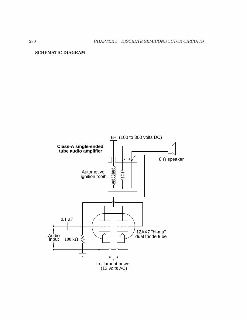
280 CHAPTER 5. DISCRETE SEMICONDUCTOR CIRCUITS
SCHEMATIC DIAGRAM
12AX7 "hi-mu" dual triode tube
to filament power(12 volts AC)
100 kΩ
0.1 µF
Audioinput
+-
B+
8 Ω speaker
Automotiveignition "coil"
(100 to 300 volts DC)
Class-A single-endedtube audio amplifier

5.19. VACUUM TUBE AUDIO AMPLIFIER 281
Fuse
(optional)
Switch
Transformer
Plug
47 µF250 WVDC
B+≈ 170 volts
DANGER! High voltage!!100 kΩ
Plate supplyswitch
Transformer
12 volt ACto filaments
Low-voltage ACpower supply
High-voltage "plate" DC power supply
120/12ratio
12/120ratio
ILLUSTRATION

282 CHAPTER 5. DISCRETE SEMICONDUCTOR CIRCUITS
Low-voltage AC power supply
6 612
12 volt
120 volt
side
side
"Plate supply"switch
-
+
- -
B+Ground
Filamentpower
Power supply
Amplifier
1
2
3
4
5
6
7
8
9
12AX7 tube
+ -
Speaker
Audioinput
INSTRUCTIONS
Welcome to the world of vacuum tube electronics! While not exactly an application of semi-conductor technology (power supply rectifier excepted), this circuit is useful as an introductionto vacuum tube technology, and an interesting application for impedance-matching transform-ers. It should be noted that building and operating this circuit involves work with
lethal voltages! You must exhibit the utmost care while working with this circuit, as 170volts DC is capable of electrocuting you!! It is recommended that beginners seek qualified as-sistance (experienced electricians, electronics technicians, or engineers) if attempting to buildthis amplifier.
WARNING: do not touch any wires or terminals while the amplifier circuit is en-
ergized! If you must make contact with the circuit at any point, turn off the ”plate” powersupply switch and wait for the filter capacitor to discharge below 30 volts before touching anypart of the circuit. If testing circuit voltages with the power on, use only one hand if possibleto avoid the possibility of an arm-to-arm electric shock.

5.19. VACUUM TUBE AUDIO AMPLIFIER 283
Building the high-voltage power supply
Vacuum tubes require fairly high DC voltage applied between plate and cathode terminalsin order to function efficiently. Although it is possible to operate the amplifier circuit describedin this experiment on as low as 24 volts DC, the power output will be miniscule and the soundquality poor. The 12AX7 triode is rated at a maximum ”plate voltage” (voltage applied betweenplate and cathode terminals) of 330 volts, so our power supply of 170 volts DC specified hereis well within that maximum limit. I’ve operated this amplifier on as high as 235 volts DC,and discovered that both sound quality and intensity improved slightly, but not enough in myestimation to warrant the additional hazard to experimenters.
The power supply actually has two different power outputs: the ”B+” DC output for platepower, and the ”filament” power, which is only 12 volts AC. Tubes require power applied toa small filament (sometimes called a heater) in order to function, as the cathode must be hotenough to thermally emit electrons, and that doesn’t happen at room temperature! Using onepower transformer to step household 120 volt AC power down to 12 volts AC provides low-voltage for the filaments, and another transformer connected in step-up fashion brings thevoltage back up to 120 volts. You might be wondering, ”why step the voltage back up to 120volts with another transformer? Why not just tap off the wall socket plug to obtain 120 voltAC power directly, and then rectify that into 170 volts DC?” The answer to this is twofold:first, running power through two transformers inherently limits the amount of current thatmay be sent into an accidental short-circuit on the plate-side of the amplifier circuit. Second, itelectrically isolates the plate circuit from the wiring system of your house. If we were to rectifywall-socket power with a diode bridge, it would make both DC terminals (+ and -) elevated involtage from the safety ground connection of your house’s electrical system, thereby increasingthe shock hazard.
Note the toggle switch connected between the 12-volt windings of the two transformers,labeled ”Plate supply switch.” This switch controls power to the step-up transformer, therebycontrolling plate voltage to the amplifier circuit. Why not just use the main power switchconnected to the 120 volt plug? Why have a second switch to shut off the DC high voltage,when shutting off one main switch would accomplish the same thing? The answer lies inproper vacuum tube operation: like incandescent light bulbs, vacuum tubes ”wear” when theirfilaments are powered up and down repeatedly, so having this additional switch in the circuitallows you to shut off the DC high voltage (for safety when modifying or adjusting the circuit)without having to shut off the filament. Also, it is a good habit to wait for the tube to reach fulloperating temperature before applying plate voltage, and this second switch allows you to delaythe application of plate voltage until the tube has had time to reach operating temperature.
During operation, you should have a voltmeter connected to the ”B+” output of the powersupply (between the B+ terminal and ground), continuously providing indication of the powersupply voltage. This meter will show you when the filter capacitor has discharged below theshock-hazard limit (30 volts) when you turn off the ”Plate supply switch” to service the ampli-fier circuit.
The ”ground” terminal shown on the DC output of the power supply circuit need not con-nect to earth ground. Rather, it is merely a symbol showing a common connection with acorresponding ground terminal symbol in the amplifier circuit. In the circuit you build, therewill be a piece of wire connecting these two ”ground” points together. As always, the designa-tion of certain common points in a circuit by means of a shared symbol is standard practice inelectronic schematics.

284 CHAPTER 5. DISCRETE SEMICONDUCTOR CIRCUITS
You will note that the schematic diagram shows a 100 kΩ resistor in parallel with the filtercapacitor. This resistor is quite necessary, as it provides the capacitor a path for discharge whenthe AC power is turned off. Without this ”bleeder” resistor in the circuit, the capacitor wouldlikely retain a dangerous charge for a long time after ”power-down,” posing an additional shockhazard to you. In the circuit I built – with a 47 µF capacitor and a 100 kΩ bleeder resistor –the time constant of this RC circuit was a brief 4.7 seconds. If you happen to find a larger filtercapacitor value (good for minimizing unwanted power supply ”hum” in the speaker), you willneed to use a correspondingly smaller value of bleeder resistor, or wait longer for the voltageto bleed off each time you turn the ”Plate supply” switch off.
Be sure you have the power supply safely constructed and working reliably before attempt-ing to power the amplifier circuit with it. This is good circuit-building practice in general:build and troubleshoot the power supply first, then build the circuit you intend to power withit. If the power supply does not function as it should, then neither will the powered circuit, nomatter how well it may be designed and built.
Building the amplifier
One of the problems with building vacuum tube circuits in the 21st century is that socketsfor these components can be difficult to find. Given the limited lifetime of most ”receiver” tubes(a few years), most ”tubed” electronic devices used sockets for mounting the tubes, so that theycould be easily removed and replaced. Though tubes may still be obtained (from music supplystores) with relative ease, the sockets they plug into are considerably scarcer – your local RadioShack will not have them in stock! How, then, do we build circuits with tubes, if we might notbe able to obtain sockets for them to plug in to?
For small tubes, this problem may be circumvented by directly soldering short lengths of22-gauge solid copper wire to the pins of the tube, thus enabling you to ”plug” the tube intoa solderless breadboard. Here is a photograph of my tube amplifier, showing the 12AX7 inan inverted position (pin-side-up). Please disregard the 10-segment LED bargraph to the leftand the 8-position DIP switch assembly to the right in the photograph, as these are leftovercomponents from a digital circuit experiment assembled previously on my breadboard.

5.19. VACUUM TUBE AUDIO AMPLIFIER 285
One benefit of mounting the tube in this position is ease of pin identification, since most”pin connection diagrams” for tubes are shown from a bottom view:
1
2
3
4
5
6
7
8
9
Cathode 1
Grid 1
Plate 1
Filamenttap
Filament 1Filament 2
Cathode 2
Grid 2
Plate 2
12AX7 dual triode tube
(view from bottom)
You will notice on the amplifier schematic that both triode elements inside the 12AX7’sglass envelope are being used, in parallel: plate connected to plate, grid connected to grid, andcathode connected to cathode. This is done to maximize power output from the tube, but itis not necessary for demonstrating basic operation. You may use just one of the triodes, forsimplicity, if you wish.
The 0.1 µF capacitor shown on the schematic ”couples” the audio signal source (radio, mu-sical keyboard, etc.) to the tube’s grid(s), allowing AC to pass but blocking DC. The 100 kΩ
resistor ensures that the average DC voltage between grid and cathode is zero, and cannot”float” to some high level. Typically, bias circuits are used to keep the grid slightly negativewith respect to ground, but for this purpose a bias circuit would introduce more complexitythan its worth.
When I tested my amplifier circuit, I used the output of a radio receiver, and later the outputof a compact disk (CD) player, as the audio signal source. Using a ”mono”-to-”phono” connectorextension cord plugged into the headphone jack of the receiver/CD player, and alligator clipjumper wires connecting the ”mono” tip of the cord to the input terminals of the tube amplifier, Iwas able to easily send the amplifier audio signals of varying amplitude to test its performanceover a wide range of conditions:

286 CHAPTER 5. DISCRETE SEMICONDUCTOR CIRCUITS
phones
"Mono" headphone
Radio
"Phono" plug
plug
. . .
. . .
Amplifier circuit
Audioinput
A transformer is essential at the output of the amplifier circuit for ”matching” the impedancesof vacuum tube and speaker. Since the vacuum tube is a high-voltage, low-current device, andmost speakers are low-voltage, high-current devices, the mismatch between them would re-sult in very audio low power output if they were directly connected. To successfully match thehigh-voltage, low-current source to the low-voltage, high current load, we must use a step-downtransformer.
Since the vacuum tube circuit’s Thevenin resistance ranges in the tens of thousands ofohms, and the speaker only has about 8 ohms impedance, we will need a transformer with animpedance ratio of about 10,000:1. Since the impedance ratio of a transformer is the square
of its turns ratio (or voltage ratio), we’re looking for a transformer with a turns ratio of about100:1. A typical automotive ignition coil has approximately this turns ratio, and it is alsorated for extremely high voltage on the high-voltage winding, making it well suited for thisapplication.
The only bad aspect of using an ignition coil is that it provides no electrical isolation be-tween primary and secondary windings, since the device is actually an autotransformer, witheach winding sharing a common terminal at one end. This means that the speaker wires will beat a high DC voltage with respect to circuit ground. So long as we know this, and avoid touch-ing those wires during operation, there will be no problem. Ideally, though, the transformerwould provide complete isolation as well as impedance matching, and the speaker wires wouldbe perfectly safe to touch during use.
Remember, make all connections in the circuit with the power turned off! After check-ing connections visually and with an ohmmeter to ensure that the circuit is built as per theschematic diagram, apply power to the filaments of the tube and wait about 30 seconds for it toreach operating temperature. The both filaments should emit a soft, orange glow, visible fromboth the top and bottom views of the tube.

5.19. VACUUM TUBE AUDIO AMPLIFIER 287
Turn the volume control of your radio/CD player/musical keyboard signal source to mini-mum, then turn on the plate supply switch. The voltmeter you have connected between thepower supply’s B+ output terminal and ”ground” should register full voltage (about 170 volts).Now, increase the volume control on the signal source and listen to the speaker. If all is well,you should hear the correct sounds clearly through the speaker.
Troubleshooting this circuit is best done with the sensitive audio detector described in theDC and AC chapters of this Experiments volume. Connect a 0.1 µF capacitor in series witheach test lead to block DC from the detector, then connect one of the test leads to ground,while using the other test lead to check for audio signal at various points in the circuit. Usecapacitors with a high voltage rating, like the one used on the input of the amplifier circuit:
plug
headphones
Sensitivity
0.1 µF
0.1 µF
Testleads
Amplifier circuit
B+
. . .. . .
"ground"
Using the sensitive audio
instrument for the amplifierdetector as a troubleshooting
Using two coupling capacitors instead of just one adds an additional degree of safety, inhelping to isolate the unit from any (high) DC voltage. Even without the extra capacitor,though, the detector’s internal transformer should provide sufficient electrical isolation foryour safety in using it to test for signals in a high-voltage circuit like this, especially if you builtyour detector using a 120 volt power transformer (rather than an ”audio output” transformer)as suggested. Use it to test for a good signal at the input, then at the grid pin(s) of the tube,then at the plate of the tube, etc. until the problem is found. Being capacitively coupled, thedetector is also able to test for excessive power supply ”hum:” touch the free test lead to thesupply’s B+ terminal and listen for a loud 60 Hz humming noise. The noise should be verysoft, not loud. If it is loud, the power supply is not filtered adequately enough, and may needadditional filter capacitance.
After testing a point in the amplifier circuit with large DC voltage to ground, the couplingcapacitors on the detector may build up substantial voltage. To discharge this voltage, brieflytouch the free test lead to the grounded test lead. A ”pop” sound should be heard in the head-phones as the coupling capacitors discharge.
If you would rather use a voltmeter to test for the presence of audio signal, you may do so,setting it to a sensitive AC voltage range. The indication you get from a voltmeter, though,

288 CHAPTER 5. DISCRETE SEMICONDUCTOR CIRCUITS
doesn’t tell you anything about the quality of the signal, just its mere presence. Bear in mindthat most AC voltmeters will register a transient voltage when initially connected across asource of DC voltage, so don’t be surprised to see a ”spike” (a strong, momentary voltage in-dication) at the very moment contact is made with the meter’s probes to the circuit, rapidlydecreasing to the true AC signal value.
You may be pleasantly surprised at the quality and depth of tone from this little amplifiercircuit, especially given its low power output: less than 1 watt of audio power. Of course, thecircuit is quite crude and sacrifices quality for simplicity and parts availability, but it servesto demonstrate the basic principle of vacuum tube amplification. Advanced hobbyists andstudents may wish to experiment with biasing networks, negative feedback, different outputtransformers, different power supply voltages, and even different tubes, to obtain more powerand/or better sound quality.
Here is a photo of a very similar amplifier circuit, built by the husband-and-wife teamof Terry and Cheryl Goetz, illustrating what can be done when care and craftsmanship areapplied to a project like this.
Bibliography
[1] Forrest M. Mims III, “Sun Photometer with Light-Emitting Diodes as Spectrally SelectiveDetectors”, Applied Optics, 31, 33, 6965-6967, 1992.
[2] Forrest M. Mims III,“Light Emitting Diodes” Howard W. Sams & Co., 1973, pp. 118-119.
[3] Forrest M. Mims III, Private communications, February 29, 2008.

Chapter 6
ANALOG INTEGRATED
CIRCUITS
Contents
6.1 Introduction . . . . . . . . . . . . . . . . . . . . . . . . . . . . . . . . . . . . . . 289
6.2 Voltage comparator . . . . . . . . . . . . . . . . . . . . . . . . . . . . . . . . . 291
6.3 Precision voltage follower . . . . . . . . . . . . . . . . . . . . . . . . . . . . . 294
6.4 Noninverting amplifier . . . . . . . . . . . . . . . . . . . . . . . . . . . . . . . 298
6.5 High-impedance voltmeter . . . . . . . . . . . . . . . . . . . . . . . . . . . . . 301
6.6 Integrator . . . . . . . . . . . . . . . . . . . . . . . . . . . . . . . . . . . . . . . 305
6.7 555 audio oscillator . . . . . . . . . . . . . . . . . . . . . . . . . . . . . . . . . . 311
6.8 555 ramp generator . . . . . . . . . . . . . . . . . . . . . . . . . . . . . . . . . 314
6.9 PWM power controller . . . . . . . . . . . . . . . . . . . . . . . . . . . . . . . 317
6.10 Class B audio amplifier . . . . . . . . . . . . . . . . . . . . . . . . . . . . . . . 321
6.1 Introduction
Analog circuits are circuits dealing with signals free to vary from zero to full power supplyvoltage. This stands in contrast to digital circuits, which almost exclusively employ ”all ornothing” signals: voltages restricted to values of zero and full supply voltage, with no validstate in between those extreme limits. Analog circuits are often referred to as linear circuitsto emphasize the valid continuity of signal range forbidden in digital circuits, but this label isunfortunately misleading. Just because a voltage or current signal is allowed to vary smoothlybetween the extremes of zero and full power supply limits does not necessarily mean that allmathematical relationships between these signals are linear in the ”straight-line” or ”propor-tional” sense of the word. As you will see in this chapter, many so-called ”linear” circuits arequite nonlinear in their behavior, either by necessity of physics or by design.
289
290 CHAPTER 6. ANALOG INTEGRATED CIRCUITS
The circuits in this chapter make use of IC, or integrated circuit, components. Such com-ponents are actually networks of interconnected components manufactured on a single waferof semiconducting material. Integrated circuits providing a multitude of pre-engineered func-tions are available at very low cost, benefitting students, hobbyists and professional circuitdesigners alike. Most integrated circuits provide the same functionality as ”discrete” semicon-ductor circuits at higher levels of reliability and at a fraction of the cost. Usually, discrete-component circuit construction is favored only when power dissipation levels are too high forintegrated circuits to handle.
Perhaps the most versatile and important analog integrated circuit for the student to mas-ter is the operational amplifier, or op-amp. Essentially nothing more than a differential am-plifier with very high voltage gain, op-amps are the workhorse of the analog design world. Bycleverly applying feedback from the output of an op-amp to one or more of its inputs, a widevariety of behaviors may be obtained from this single device. Many different models of op-ampare available at low cost, but circuits described in this chapter will incorporate only commonlyavailable op-amp models.

6.2. VOLTAGE COMPARATOR 291
6.2 Voltage comparator
PARTS AND MATERIALS
• Operational amplifier, model 1458 or 353 recommended (Radio Shack catalog # 276-038and 900-6298, respectively)
• Three 6 volt batteries
• Two 10 kΩ potentiometers, linear taper (Radio Shack catalog # 271-1715)
• One light-emitting diode (Radio Shack catalog # 276-026 or equivalent)
• One 330 Ω resistor
• One 470 Ω resistor
This experiment only requires a single operational amplifier. The model 1458 and 353 areboth ”dual” op-amp units, with two complete amplifier circuits housed in the same 8-pin DIPpackage. I recommend that you purchase and use ”dual” op-amps over ”single” op-amps even ifa project only requires one, because they are more versatile (the same op-amp unit can functionin projects requiring only one amplifier as well as in projects requiring two). In the interest ofpurchasing and stocking the least number of components for your home laboratory, this makessense.
CROSS-REFERENCES
Lessons In Electric Circuits, Volume 3, chapter 8: ”Operational Amplifiers”
LEARNING OBJECTIVES
• How to use an op-amp as a comparator
SCHEMATIC DIAGRAM
−
+
330 Ω 470 Ω1/2 1458
6 V
6 V
6 V

292 CHAPTER 6. ANALOG INTEGRATED CIRCUITS
ILLUSTRATION
+-
+-
+-
1458
INSTRUCTIONS
A comparator circuit compares two voltage signals and determines which one is greater.The result of this comparison is indicated by the output voltage: if the op-amp’s output issaturated in the positive direction, the noninverting input (+) is a greater, or more positive,voltage than the inverting input (-), all voltages measured with respect to ground. If the op-amp’s voltage is near the negative supply voltage (in this case, 0 volts, or ground potential), itmeans the inverting input (-) has a greater voltage applied to it than the noninverting input(+).
This behavior is much easier understood by experimenting with a comparator circuit thanit is by reading someone’s verbal description of it. In this experiment, two potentiometerssupply variable voltages to be compared by the op-amp. The output status of the op-amp isindicated visually by the LED. By adjusting the two potentiometers and observing the LED,one can easily comprehend the function of a comparator circuit.
For greater insight into this circuit’s operation, you might want to connect a pair of volt-meters to the op-amp input terminals (both voltmeters referenced to ground) so that both inputvoltages may be numerically compared with each other, these meter indications compared tothe LED status:

6.2. VOLTAGE COMPARATOR 293
+-
+-
+-
1458
V Ω
COMA
V Ω
COMA
Comparator circuits are widely used to compare physical measurements, provided thosephysical variables can be translated into voltage signals. For instance, if a small generatorwere attached to an anemometer wheel to produce a voltage proportional to wind speed, thatwind speed signal could be compared with a ”set-point” voltage and compared by an op-amp todrive a high wind speed alarm:
−
+
330 Ω 470 Ω1/2 1458
6 V
6 V
6 V Gen
+
-
LED lights up when wind speed exceeds"set-point" limit established by the
potentiometer position.

294 CHAPTER 6. ANALOG INTEGRATED CIRCUITS
6.3 Precision voltage follower
PARTS AND MATERIALS
• Operational amplifier, model 1458 or 353 recommended (Radio Shack catalog # 276-038and 900-6298, respectively)
• Three 6 volt batteries
• One 10 kΩ potentiometer, linear taper (Radio Shack catalog # 271-1715)
CROSS-REFERENCES
Lessons In Electric Circuits, Volume 3, chapter 8: ”Operational Amplifiers”
LEARNING OBJECTIVES
• How to use an op-amp as a voltage follower
• Purpose of negative feedback
• Troubleshooting strategy
SCHEMATIC DIAGRAM
−
+
1/2 1458
6 V
6 V
6 V VinputVoutput
ILLUSTRATION
6.3. PRECISION VOLTAGE FOLLOWER 295
+-
+-
+-
1458
INSTRUCTIONS
In the previous op-amp experiment, the amplifier was used in ”open-loop” mode; that is,without any feedback from output to input. As such, the full voltage gain of the operationalamplifier was available, resulting in the output voltage saturating for virtually any amountof differential voltage applied between the two input terminals. This is good if we desire com-parator operation, but if we want the op-amp to behave as a true amplifier, we need it to exhibita manageable voltage gain.
Since we do not have the luxury of disassembling the integrated circuitry of the op-ampand changing resistor values to give a lesser voltage gain, we are limited to external connec-tions and componentry. Actually, this is not a disadvantage as one might think, because thecombination of extremely high open-loop voltage gain coupled with feedback allows us to usethe op-amp for a much wider variety of purposes, much easier than if we were to exercise theoption of modifying its internal circuitry.
If we connect the output of an op-amp to its inverting (-) input, the output voltage will seekwhatever level is necessary to balance the inverting input’s voltage with that applied to thenoninverting (+) input. If this feedback connection is direct, as in a straight piece of wire,the output voltage will precisely ”follow” the noninverting input’s voltage. Unlike the voltage
follower circuit made from a single transistor (see chapter 5: Discrete Semiconductor Circuits),which approximated the input voltage to within several tenths of a volt, this voltage followercircuit will output a voltage accurate to within mere microvolts of the input voltage!
Measure the input voltage of this circuit with a voltmeter connected between the op-amp’snoninverting (+) input terminal and circuit ground (the negative side of the power supply),and the output voltage between the op-amp’s output terminal and circuit ground. Watch theop-amp’s output voltage follow the input voltage as you adjust the potentiometer through itsrange.
296 CHAPTER 6. ANALOG INTEGRATED CIRCUITS
You may directly measure the difference, or error, between output and input voltages byconnecting the voltmeter between the op-amp’s two input terminals. Throughout most of thepotentiometer’s range, this error voltage should be almost zero.
Try moving the potentiometer to one of its extreme positions, far clockwise or far counter-clockwise. Measure error voltage, or compare output voltage against input voltage. Do younotice anything unusual? If you are using the model 1458 or model 353 op-amp for this ex-periment, you should measure a substantial error voltage, or difference between output andinput. Many op-amps, the specified models included, cannot ”swing” their output voltage ex-actly to full power supply (”rail”) voltage levels. In this case, the ”rail” voltages are +18 voltsand 0 volts, respectively. Due to limitations in the 1458’s internal circuitry, its output voltageis unable to exactly reach these high and low limits. You may find that it can only go withina volt or two of the power supply ”rails.” This is a very important limitation to understandwhen designing circuits using operational amplifiers. If full ”rail-to-rail” output voltage swingis required in a circuit design, other op-amp models may be selected which offer this capability.The model 3130 is one such op-amp.
Precision voltage follower circuits are useful if the voltage signal to be amplified cannot tol-erate ”loading;” that is, if it has a high source impedance. Since a voltage follower by definitionhas a voltage gain of 1, its purpose has nothing to do with amplifying voltage, but rather withamplifying a signal’s capacity to deliver current to a load.
Voltage follower circuits have another important use for circuit builders: they allow forsimple linear testing of an op-amp. One of the troubleshooting techniques I recommend isto simplify and rebuild. Suppose that you are building a circuit using one or more op-ampsto perform some advanced function. If one of those op-amps seems to be causing a problemand you suspect it may be faulty, try re-connecting it as a simple voltage follower and see if itfunctions in that capacity. An op-amp that fails to work as a voltage follower certainly won’twork as anything more complex!
COMPUTER SIMULATION
Schematic with SPICE node numbers:
−
+
Vinput
0 0
1
Rload
E12
2
Rbogus
Netlist (make a text file containing the following text, verbatim):Voltage followervinput 1 0rbogus 1 0 1mege1 2 0 1 2 999meg

6.3. PRECISION VOLTAGE FOLLOWER 297
rload 2 0 10k.dc vinput 5 5 1.print dc v(1,0) v(2,0) v(1,2).end
An ideal operational amplifier may be simulated in SPICE using a dependent voltage source
(e1 in the netlist). The output nodes are specified first (2 0), then the two input nodes, non-inverting input first (1 2). Open-loop gain is specified last (999meg) in the dependent voltagesource line.
Because SPICE views the input impedance of a dependent source as infinite, some finiteamount of resistance must be included to avoid an analysis error. This is the purpose of Rbogus:to provide DC path to ground for the Vinput voltage source. Such ”bogus” resistances should bearbitrarily large. In this simulation I chose 1 MΩ for an Rbogus value.
A load resistor is included in the circuit for much the same reason: to provide a DC path forcurrent at the output of the dependent voltage source. As you can see, SPICE doesn’t like opencircuits!

298 CHAPTER 6. ANALOG INTEGRATED CIRCUITS
6.4 Noninverting amplifier
PARTS AND MATERIALS
• Operational amplifier, model 1458 or 353 recommended (Radio Shack catalog # 276-038and 900-6298, respectively)
• Three 6 volt batteries
• Two 10 kΩ potentiometers, linear taper (Radio Shack catalog # 271-1715)
CROSS-REFERENCES
Lessons In Electric Circuits, Volume 3, chapter 8: ”Operational Amplifiers”
LEARNING OBJECTIVES
• How to use an op-amp as a single-ended amplifier
• Using divided, negative feedback
SCHEMATIC DIAGRAM
−
+
1/2 1458
6 V
6 V
6 V VinputVoutput
R1
R2
ILLUSTRATION

6.4. NONINVERTING AMPLIFIER 299
+-
+-
+-
1458
INSTRUCTIONS
This circuit differs from the voltage follower in only one respect: output voltage is ”fed back”to the inverting (-) input through a voltage-dividing potentiometer rather than being directlyconnected. With only a fraction of the output voltage fed back to the inverting input, the op-amp will output a corresponding multiple of the voltage sensed at the noninverting (+) input inkeeping the input differential voltage near zero. In other words, the op-amp will now functionas an amplifier with a controllable voltage gain, that gain being established by the position ofthe feedback potentiometer (R2).
Set R2 to approximately mid-position. This should give a voltage gain of about 2. Measureboth input and output voltage for several positions of the input potentiometer R1. Move R2 to adifferent position and re-take voltage measurements for several positions of R1. For any givenR2 position, the ratio between output and input voltage should be the same.
You will also notice that the input and output voltages are always positive with respect toground. Because the output voltage increases in a positive direction for a positive increase ofthe input voltage, this amplifier is referred to as noninverting. If the output and input voltageswere related to one another in an inverse fashion (i.e. positive increasing input voltage resultsin positive decreasing or negative increasing output), then the amplifier would be known as aninverting type.
The ability to leverage an op-amp in this fashion to create an amplifier with controllablevoltage gain makes this circuit an extremely useful one. It would take quite a bit more designand troubleshooting effort to produce a similar circuit using discrete transistors.
Try adjusting R2 for maximum and minimum voltage gain. What is the lowest voltage gainattainable with this amplifier configuration? Why do you think this is?
COMPUTER SIMULATION

300 CHAPTER 6. ANALOG INTEGRATED CIRCUITS
Schematic with SPICE node numbers:
−
+
Vinput
00
1
Rload
E1
2
Rbogus
0
3
32 R2R1
Netlist (make a text file containing the following text, verbatim):Noninverting amplifiervinput 1 0r2 3 2 5kr1 2 0 5krbogus 1 0 1mege1 3 0 1 2 999megrload 3 0 10k.dc vinput 5 5 1.print dc v(1,0) v(3,0).end
With R1 and R2 set equally to 5 kΩ in the simulation, it mimics the feedback potentiometerof the real circuit at mid-position (50%). To simulate the potentiometer at the 75% position,set R2 to 7.5 kΩ and R1 to 2.5 kΩ.

6.5. HIGH-IMPEDANCE VOLTMETER 301
6.5 High-impedance voltmeter
PARTS AND MATERIALS
• Operational amplifier, model TL082 recommended (Radio Shack catalog # 276-1715)
• Operational amplifier, model LM1458 recommended (Radio Shack catalog # 276-038)
• Four 6 volt batteries
• One meter movement, 1 mA full-scale deflection (Radio Shack catalog #22-410)
• 15 kΩ precision resistor
• Four 1 MΩ resistors
The 1 mA meter movement sold by Radio Shack is advertised as a 0-15 VDC meter, but isactually a 1 mA movement sold with a 15 kΩ +/- 1% tolerance multiplier resistor. If you getthis Radio Shack meter movement, you can use the included 15 kΩ resistor for the resistorspecified in the parts list.
This meter experiment is based on a JFET-input op-amp such as the TL082. The other op-amp (model 1458) is used in this experiment to demonstrate the absence of latch-up: a probleminherent to the TL082.
You don’t need 1 MΩ resistors, exactly. Any very high resistance resistors will suffice.
CROSS-REFERENCES
Lessons In Electric Circuits, Volume 3, chapter 8: ”Operational Amplifiers”
LEARNING OBJECTIVES
• Voltmeter loading: its causes and its solution
• How to make a high-impedance voltmeter using an op-amp
• What op-amp ”latch-up” is and how to avoid it
SCHEMATIC DIAGRAM

302 CHAPTER 6. ANALOG INTEGRATED CIRCUITS
−
+
0-1 mA15 kΩ 1 MΩ
1 MΩ
1 MΩ
1 MΩTP1
TP2
TP3
+-
TL082
6 V
6 V
6 V
6 V
Testprobe
ILLUSTRATION
+-
+-
+-
+-
TL082
- +
0 to 1 mAmeter
movement
TP1TP2TP3
INSTRUCTIONS
An ideal voltmeter has infinite input impedance, meaning that it draws zero current fromthe circuit under test. This way, there will be no ”impact” on the circuit as the voltage is

6.5. HIGH-IMPEDANCE VOLTMETER 303
being measured. The more current a voltmeter draws from the circuit under test, the more themeasured voltage will ”sag” under the loading effect of the meter, like a tire-pressure gaugereleasing air out of the tire being measured: the more air released from the tire, the more thetire’s pressure will be impacted in the act of measurement. This loading is more pronouncedon circuits of high resistance, like the voltage divider made of 1 MΩ resistors, shown in theschematic diagram.
If you were to build a simple 0-15 volt range voltmeter by connecting the 1 mA metermovement in series with the 15 kΩ precision resistor, and try to use this voltmeter to measurethe voltages at TP1, TP2, or TP3 (with respect to ground), you’d encounter severemeasurementerrors induced by meter ”impact:”
0-1 mA
1 MΩ
1 MΩ
1 MΩ
1 MΩTP1
TP2
TP3
+-
6 V
6 V
TP1 should be 3 voltsTP2 should be 6 voltsTP3 should be 9 volts
However, the meter will fail tomeasure these voltages correctly
due to the meter’s "loading" effect!
15 kΩ
Try using the meter movement and 15 kΩ resistor as shown to measure these three volt-ages. Does the meter read falsely high or falsely low? Why do you think this is?
If we were to increase the meter’s input impedance, we would diminish its current drawor ”load” on the circuit under test and consequently improve its measurement accuracy. Anop-amp with high-impedance inputs (using a JFET transistor input stage rather than a BJTinput stage) works well for this application.
Note that the meter movement is part of the op-amp’s feedback loop from output to invert-ing input. This circuit drives the meter movement with a current proportional to the voltageimpressed at the noninverting (+) input, the requisite current supplied directly from the bat-teries through the op-amp’s power supply pins, not from the circuit under test through the testprobe. The meter’s range is set by the resistor connecting the inverting (-) input to ground.
Build the op-amp meter circuit as shown and re-take voltage measurements at TP1, TP2,and TP3. You should enjoy far better success this time, with the meter movement accuratelymeasuring these voltages (approximately 3, 6, and 9 volts, respectively).
You may witness the extreme sensitivity of this voltmeter by touching the test probe withone hand and the most positive battery terminal with the other. Notice how you can drive theneedle upward on the scale simply by measuring battery voltage through your body resistance:an impossible feat with the original, unamplified voltmeter circuit. If you touch the test probeto ground, the meter should read exactly 0 volts.

304 CHAPTER 6. ANALOG INTEGRATED CIRCUITS
After you’ve proven this circuit to work, modify it by changing the power supply from dualto split. This entails removing the center-tap ground connection between the 2nd and 3rdbatteries, and grounding the far negative battery terminal instead:
−
+
0-1 mA15 kΩ 1 MΩ
1 MΩ
1 MΩ
1 MΩTP1
TP2
TP3
+-
TL082
6 V
6 V
6 V
6 V
This alteration in the power supply increases the voltages at TP1, TP2, and TP3 to 6, 12,and 18 volts, respectively. With a 15 kΩ range resistor and a 1 mAmeter movement, measuring18 volts will gently ”peg” the meter, but you should be able to measure the 6 and 12 volt testpoints just fine.
Try touching the meter’s test probe to ground. This should drive the meter needle to exactly0 volts as before, but it will not! What is happening here is an op-amp phenomenon calledlatch-up: where the op-amp output drives to a positive voltage when the input common-modevoltage exceeds the allowable limit. In this case, as with many JFET-input op-amps, neitherinput should be allowed to come close to either power supply rail voltage. With a single supply,the op-amp’s negative power rail is at ground potential (0 volts), so grounding the test probebrings the noninverting (+) input exactly to that rail voltage. This is bad for a JFET op-amp,and drives the output strongly positive, even though it doesn’t seem like it should, based onhow op-amps are supposed to function.
When the op-amp ran on a ”dual” supply (+12/-12 volts, rather than a ”single” +24 volt sup-ply), the negative power supply rail was 12 volts away from ground (0 volts), so grounding thetest probe didn’t violate the op-amp’s common-mode voltage limit. However, with the ”single”+24 volt supply, we have a problem. Note that some op-amps do not ”latch-up” the way themodel TL082 does. You may replace the TL082 with an LM1458 op-amp, which is pin-for-pincompatible (no breadboard wiring changes needed). The model 1458 will not ”latch-up” whenthe test probe is grounded, although you may still get incorrect meter readings with the mea-sured voltage exactly equal to the negative power supply rail. As a general rule, you shouldalways be sure the op-amp’s power supply rail voltages exceed the expected input voltages.

6.6. INTEGRATOR 305
6.6 Integrator
PARTS AND MATERIALS
• Four 6 volt batteries
• Operational amplifier, model 1458 recommended (Radio Shack catalog # 276-038)
• One 10 kΩ potentiometer, linear taper (Radio Shack catalog # 271-1715)
• Two capacitors, 0.1 µF each, non-polarized (Radio Shack catalog # 272-135)
• Two 100 kΩ resistors
• Three 1 MΩ resistors
Just about any operational amplifier model will work fine for this integrator experiment,but I’m specifying the model 1458 over the 353 because the 1458 has much higher input biascurrents. Normally, high input bias current is a bad characteristic for an op-amp to have in aprecision DC amplifier circuit (and especially an integrator circuit!). However, I want the biascurrent to be high in order that its bad effects may be exaggerated, and so that you will learnone method of counteracting its effects.
CROSS-REFERENCES
Lessons In Electric Circuits, Volume 3, chapter 8: ”Operational Amplifiers”
LEARNING OBJECTIVES
• Method for limiting the span of a potentiometer
• Purpose of an integrator circuit
• How to compensate for op-amp bias current
SCHEMATIC DIAGRAM
−
+
1/2 14586 V
6 V
6 V
Voutput
6 V100 kΩ
100 kΩ
10 kΩ
1 MΩ
1 MΩ
0.1 µF

306 CHAPTER 6. ANALOG INTEGRATED CIRCUITS
ILLUSTRATION
+-
+-
+-
1458
+-
INSTRUCTIONS
As you can see from the schematic diagram, the potentiometer is connected to the ”rails”of the power source through 100 kΩ resistors, one on each end. This is to limit the span ofthe potentiometer, so that full movement produces a fairly small range of input voltages forthe op-amp to operate on. At one extreme of the potentiometer’s motion, a voltage of about0.5 volt (with respect the the ground point in the middle of the series battery string) will beproduced at the potentiometer wiper. At the other extreme of motion, a voltage of about -0.5volt will be produced. When the potentiometer is positioned dead-center, the wiper voltageshould measure zero volts.
Connect a voltmeter between the op-amp’s output terminal and the circuit ground point.Slowly move the potentiometer control while monitoring the output voltage. The output voltageshould be changing at a rate established by the potentiometer’s deviation from zero (center)position. To use calculus terms, we would say that the output voltage represents the integral
(with respect to time) of the input voltage function. That is, the input voltage level establishesthe output voltage rate of change over time. This is precisely the opposite of differentiation,where the derivative of a signal or function is its instantaneous rate of change.
If you have two voltmeters, you may readily see this relationship between input voltageand output voltage rate of change by measuring the wiper voltage (between the potentiometer
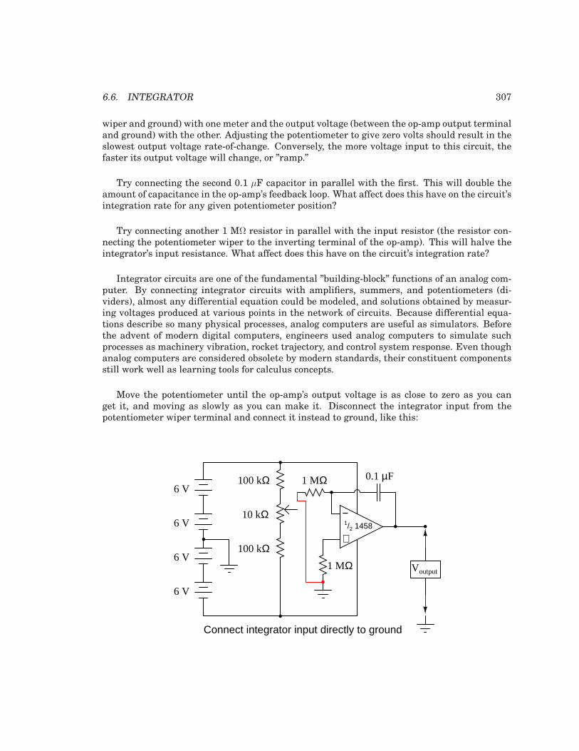
6.6. INTEGRATOR 307
wiper and ground) with one meter and the output voltage (between the op-amp output terminaland ground) with the other. Adjusting the potentiometer to give zero volts should result in theslowest output voltage rate-of-change. Conversely, the more voltage input to this circuit, thefaster its output voltage will change, or ”ramp.”
Try connecting the second 0.1 µF capacitor in parallel with the first. This will double theamount of capacitance in the op-amp’s feedback loop. What affect does this have on the circuit’sintegration rate for any given potentiometer position?
Try connecting another 1 MΩ resistor in parallel with the input resistor (the resistor con-necting the potentiometer wiper to the inverting terminal of the op-amp). This will halve theintegrator’s input resistance. What affect does this have on the circuit’s integration rate?
Integrator circuits are one of the fundamental ”building-block” functions of an analog com-puter. By connecting integrator circuits with amplifiers, summers, and potentiometers (di-viders), almost any differential equation could be modeled, and solutions obtained by measur-ing voltages produced at various points in the network of circuits. Because differential equa-tions describe so many physical processes, analog computers are useful as simulators. Beforethe advent of modern digital computers, engineers used analog computers to simulate suchprocesses as machinery vibration, rocket trajectory, and control system response. Even thoughanalog computers are considered obsolete by modern standards, their constituent componentsstill work well as learning tools for calculus concepts.
Move the potentiometer until the op-amp’s output voltage is as close to zero as you canget it, and moving as slowly as you can make it. Disconnect the integrator input from thepotentiometer wiper terminal and connect it instead to ground, like this:
−
+
1/2 14586 V
6 V
6 V
Voutput
6 V100 kΩ
100 kΩ
10 kΩ
1 MΩ
1 MΩ
Connect integrator input directly to ground
0.1 µF
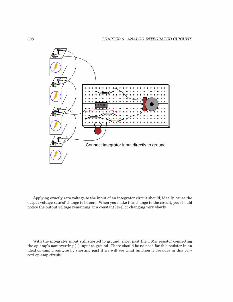
308 CHAPTER 6. ANALOG INTEGRATED CIRCUITS
+-
+-
+-
1458
+-
Connect integrator input directly to ground
Applying exactly zero voltage to the input of an integrator circuit should, ideally, cause theoutput voltage rate-of-change to be zero. When you make this change to the circuit, you shouldnotice the output voltage remaining at a constant level or changing very slowly.
With the integrator input still shorted to ground, short past the 1 MΩ resistor connectingthe op-amp’s noninverting (+) input to ground. There should be no need for this resistor in anideal op-amp circuit, so by shorting past it we will see what function it provides in this veryreal op-amp circuit:

6.6. INTEGRATOR 309
−
+
1/2 14586 V
6 V
6 V
Voutput
6 V100 kΩ
100 kΩ
10 kΩ
1 MΩ
1 MΩ
Connect integrator input directly to groundShort past the "grounding" resistor
0.1 µF
+-
+-
+-
1458
+-
Connect integrator input directly to groundShort past the "grounding" resistor
As soon as the ”grounding” resistor is shorted with a jumper wire, the op-amp’s outputvoltage will start to change, or drift. Ideally, this should not happen, because the integrator

310 CHAPTER 6. ANALOG INTEGRATED CIRCUITS
circuit still has an input signal of zero volts. However, real operational amplifiers have avery small amount of current entering each input terminal called the bias current. These biascurrents will drop voltage across any resistance in their path. Since the 1 MΩ input resistorconducts some amount of bias current regardless of input signal magnitude, it will drop voltageacross its terminals due to bias current, thus ”offsetting” the amount of signal voltage seen atthe inverting terminal of the op-amp. If the other (noninverting) input is connected directly toground as we have done here, this ”offset” voltage incurred by voltage drop generated by biascurrent will cause the integrator circuit to slowly ”integrate” as though it were receiving a verysmall input signal.
The ”grounding” resistor is better known as a compensating resistor, because it acts tocompensate for voltage errors created by bias current. Since the bias currents through eachop-amp input terminal are approximately equal to each other, an equal amount of resistanceplaced in the path of each bias current will produce approximately the same voltage drop.Equal voltage drops seen at the complementary inputs of an op-amp cancel each other out,thus nulling the error otherwise induced by bias current.
Remove the jumper wire shorting past the compensating resistor and notice how the op-amp output returns to a relatively stable state. It may still drift some, most likely due to bias
voltage error in the op-amp itself, but that is another subject altogether!
COMPUTER SIMULATION
Schematic with SPICE node numbers:
−
+
1 MΩ 0.1 µF1
0 0
23
Netlist (make a text file containing the following text, verbatim):DC integratorvinput 1 0 dc 0.05r1 1 2 1megc1 2 3 0.1u ic=0e1 3 0 0 2 999k.tran 1 30 uic.plot tran v(1,0) v(3,0).end

6.7. 555 AUDIO OSCILLATOR 311
6.7 555 audio oscillator
PARTS AND MATERIALS
• Two 6 volt batteries
• One capacitor, 0.1 µF, non-polarized (Radio Shack catalog # 272-135)
• One 555 timer IC (Radio Shack catalog # 276-1723)
• Two light-emitting diodes (Radio Shack catalog # 276-026 or equivalent)
• One 1 MΩ resistor
• One 100 kΩ resistor
• Two 510 Ω resistors
• Audio detector with headphones
• Oscilloscope (recommended, but not necessary)
A oscilloscope would be useful in analyzing the waveforms produced by this circuit, but itis not essential. An audio detector is a very useful piece of test equipment for this experiment,especially if you don’t have an oscilloscope.
CROSS-REFERENCES
Lessons In Electric Circuits, Volume 4, chapter 10: ”Multivibrators”
LEARNING OBJECTIVES
• How to use the 555 timer as an astable multivibrator
• Working knowledge of duty cycle
SCHEMATIC DIAGRAM
555Disch
Thresh
Trig
Gnd
Vcc RST
Out
Ctrl
6 V
6 V
0.1 µF
1 MΩ
100 kΩ
510 Ω
510 Ω

312 CHAPTER 6. ANALOG INTEGRATED CIRCUITS
ILLUSTRATION
555
+-
+-
INSTRUCTIONS
The ”555” integrated circuit is a general-purpose timer useful for a variety of functions. Inthis experiment, we explore its use as an astable multivibrator, or oscillator. Connected to acapacitor and two resistors as shown, it will oscillate freely, driving the LEDs on and off witha square-wave output voltage.
This circuit works on the principle of alternately charging and discharging a capacitor. The555 begins to discharge the capacitor by grounding the Disch terminal when the voltage de-tected by the Thresh terminal exceeds 2/3 the power supply voltage (Vcc). It stops dischargingthe capacitor when the voltage detected by the Trig terminal falls below 1/3 the power supplyvoltage. Thus, when both Thresh and Trig terminals are connected to the capacitor’s posi-tive terminal, the capacitor voltage will cycle between 1/3 and 2/3 power supply voltage in a”sawtooth” pattern.
During the charging cycle, the capacitor receives charging current through the series com-bination of the 1 MΩ and 100 kΩ resistors. As soon as the Disch terminal on the 555 timer goesto ground potential (a transistor inside the 555 connected between that terminal and groundturns on), the capacitor’s discharging current only has to go through the 100 kΩ resistor. Theresult is an RC time constant that is much longer for charging than for discharging, resultingin a charging time greatly exceeding the discharging time.
The 555’s Out terminal produces a square-wave voltage signal that is ”high” (nearly Vcc)when the capacitor is charging, and ”low” (nearly 0 volts) when the capacitor is discharging.This alternating high/low voltage signal drives the two LEDs in opposite modes: when one ison, the other will be off. Because the capacitor’s charging and discharging times are unequal,the ”high” and ”low” times of the output’s square-wave waveform will be unequal as well. Thiscan be seen in the relative brightness of the two LEDs: one will be much brighter than theother, because it is on for a longer period of time during each cycle.
The equality or inequality between ”high” and ”low” times of a square wave is expressedas that wave’s duty cycle. A square wave with a 50% duty cycle is perfectly symmetrical: its”high” time is precisely equal to its ”low” time. A square wave that is ”high” 10% of the time

6.7. 555 AUDIO OSCILLATOR 313
and ”low” 90% of the time is said to have a 10% duty cycle. In this circuit, the output waveformhas a ”high” time exceeding the ”low” time, resulting in a duty cycle greater than 50%.
Use the audio detector (or an oscilloscope) to investigate the different voltage waveformsproduced by this circuit. Try different resistor values and/or capacitor values to see whateffects they have on output frequency or charge/discharge times.

314 CHAPTER 6. ANALOG INTEGRATED CIRCUITS
6.8 555 ramp generator
PARTS AND MATERIALS
• Two 6 volt batteries
• One capacitor, 470 µF electrolytic, 35 WVDC (Radio Shack catalog # 272-1030 or equiva-lent)
• One capacitor, 0.1 µF, non-polarized (Radio Shack catalog # 272-135)
• One 555 timer IC (Radio Shack catalog # 276-1723)
• Two PNP transistors – models 2N2907 or 2N3906 recommended (Radio Shack catalog #276-1604 is a package of fifteen PNP transistors ideal for this and other experiments)
• Two light-emitting diodes (Radio Shack catalog # 276-026 or equivalent)
• One 100 kΩ resistor
• One 47 kΩ resistor
• Two 510 Ω resistors
• Audio detector with headphones
The voltage rating on the 470 µF capacitor is not critical, so long as it generously exceedsthe maximum power supply voltage. In this particular circuit, that maximum voltage is 12volts. Be sure you connect this capacitor in the circuit properly, respecting polarity!
CROSS-REFERENCES
Lessons In Electric Circuits, Volume 1, chapter 13: ”Capacitors”
Lessons In Electric Circuits, Volume 4, chapter 10: ”Multivibrators”
LEARNING OBJECTIVES
• How to use the 555 timer as an astable multivibrator
• A practical use for a current mirror circuit
• Understanding the relationship between capacitor current and capacitor voltage rate-of-change
SCHEMATIC DIAGRAM

6.8. 555 RAMP GENERATOR 315
555Disch
Thresh
Trig
Gnd
Vcc RST
Out
Ctrl
6 V
6 V100 kΩ
510 Ω
510 ΩTP1
TP3
+A
-
TP2
47 kΩ
470 µF
ILLUSTRATION
555
+-
+- CBE
CBE
--
TP2
TP3
TP1
INSTRUCTIONS
Again, we are using a 555 timer IC as an astable multivibrator, or oscillator. This time,however, we will compare its operation in two different capacitor-charging modes: traditionalRC and constant-current.
Connecting test point #1 (TP1) to test point #3 (TP3) using a jumper wire. This allowsthe capacitor to charge through a 47 kΩ resistor. When the capacitor has reached 2/3 supplyvoltage, the 555 timer switches to ”discharge” mode and discharges the capacitor to a level of1/3 supply voltage almost immediately. The charging cycle begins again at this point. Measurevoltage directly across the capacitor with a voltmeter (a digital voltmeter is preferred), andnote the rate of capacitor charging over time. It should rise quickly at first, then taper off as itbuilds up to 2/3 supply voltage, just as you would expect from an RC charging circuit.
Remove the jumper wire from TP3, and re-connect it to TP2. This allows the capacitor tobe charged through the controlled-current leg of a current mirror circuit formed by the twoPNP transistors. Measure voltage directly across the capacitor again, noting the difference incharging rate over time as compared to the last circuit configuration.

316 CHAPTER 6. ANALOG INTEGRATED CIRCUITS
By connecting TP1 to TP2, the capacitor receives a nearly constant charging current. Con-stant capacitor charging current yields a voltage curve that is linear, as described by the equa-tion i = C(de/dt). If the capacitor’s current is constant, so will be its rate-of-change of voltageover time. The result is a ”ramp” waveform rather than a ”sawtooth” waveform:
Sawtooth waveform (RC circuit)
Ramp waveform (constant current)The capacitor’s charging current may be directly measured by substituting an ammeter in
place of the jumper wire. The ammeter will need to be set to measure a current in the range ofhundreds of microamps (tenths of a milliamp). Connected between TP1 and TP3, you shouldsee a current that starts at a relatively high value at the beginning of the charging cycle, andtapers off toward the end. Connected between TP1 and TP2, however, the current will be muchmore stable.
It is an interesting experiment at this point to change the temperature of either currentmirror transistor by touching it with your finger. As the transistor warms, it will conduct morecollector current for the same base-emitter voltage. If the controlling transistor (the one con-nected to the 100 kΩ resistor) is touched, the current decreases. If the controlled transistor istouched, the current increases. For the most stable current mirror operation, the two transis-tors should be cemented together so that their temperatures never differ by any substantialamount.
This circuit works just as well at high frequencies as it does at low frequencies. Replacethe 470 µF capacitor with a 0.1 µF capacitor, and use an audio detector to sense the voltagewaveform at the 555’s output terminal. The detector should produce an audio tone that is easyto hear. The capacitor’s voltage will now be changing much too fast to view with a voltmeter inthe DC mode, but we can still measure capacitor current with an ammeter.
With the ammeter connected between TP1 and TP3 (RC mode), measure both DC mi-croamps and AC microamps. Record these current figures on paper. Now, connect the am-meter between TP1 and TP2 (constant-current mode). Measure both DC microamps and ACmicroamps, noting any differences in current readings between this circuit configuration andthe last one. Measuring AC current in addition to DC current is an easy way to determinewhich circuit configuration gives the most stable charging current. If the current mirror cir-cuit were perfect – the capacitor charging current absolutely constant – there would be zeroAC current measured by the meter.

6.9. PWM POWER CONTROLLER 317
6.9 PWM power controller
PARTS AND MATERIALS
• Four 6 volt batteries
• One capacitor, 100 µF electrolytic, 35 WVDC (Radio Shack catalog # 272-1028 or equiva-lent)
• One capacitor, 0.1 µF, non-polarized (Radio Shack catalog # 272-135)
• One 555 timer IC (Radio Shack catalog # 276-1723)
• Dual operational amplifier, model 1458 recommended (Radio Shack catalog # 276-038)
• One NPN power transistor – (Radio Shack catalog # 276-2041 or equivalent)
• Three 1N4001 rectifying diodes (Radio Shack catalog # 276-1101)
• One 10 kΩ potentiometer, linear taper (Radio Shack catalog # 271-1715)
• One 33 kΩ resistor
• 12 volt automotive tail-light lamp
• Audio detector with headphones
CROSS-REFERENCES
Lessons In Electric Circuits, Volume 3, chapter 8: ”Operational Amplifiers”Lessons In Electric Circuits, Volume 2, chapter 7: ”Mixed-Frequency AC Signals”
LEARNING OBJECTIVES
• How to use the 555 timer as an astable multivibrator
• How to use an op-amp as a comparator
• How to use diodes to drop unwanted DC voltage
• How to control power to a load by pulse-width modulation
SCHEMATIC DIAGRAM
555Disch
Thresh
Trig
Gnd
Vcc RST
Out
Ctrl
6 V
6 V
33 kΩ
0.1 µF
6 V
6 V−
+
Load
Powertransistor
−
+
14581/2
14581/2

318 CHAPTER 6. ANALOG INTEGRATED CIRCUITS
ILLUSTRATION
+-
+-
+-
+-
555
EB
C
1458
INSTRUCTIONS
This circuit uses a 555 timer to generate a sawtooth voltage waveform across a capacitor,then compares that signal against a steady voltage provided by a potentiometer, using an op-amp as a comparator. The comparison of these two voltage signals produces a square-waveoutput from the op-amp, varying in duty cycle according to the potentiometer’s position. Thisvariable duty cycle signal then drives the base of a power transistor, switching current on andoff through the load. The 555’s oscillation frequency is much higher than the lamp filament’sability to thermally cycle (heat and cool), so any variation in duty cycle, or pulse width, has theeffect of controlling the total power dissipated by the load over time.

6.9. PWM POWER CONTROLLER 319
EC
EC
Controlvoltage
Output (high power to load)
Output (low power to load)
Controlling electrical power through a load by means of quickly switching it on and off,and varying the ”on” time, is known as pulse-width modulation, or PWM. It is a very efficientmeans of controlling electrical power because the controlling element (the power transistor)dissipates comparatively little power in switching on and off, especially if compared to thewasted power dissipated of a rheostat in a similar situation. When the transistor is in cutoff,its power dissipation is zero because there is no current through it. When the transistor issaturated, its dissipation is very low because there is little voltage dropped between collectorand emitter while it is conducting current.
PWM is a concept easier understood through experimentation than reading. It would benice to view the capacitor voltage, potentiometer voltage, and op-amp output waveforms allon one (triple-trace) oscilloscope to see how they relate to one another, and to the load power.However, most of us have no access to a triple-trace oscilloscope, much less any oscilloscope atall, so an alternative method is to slow the 555 oscillator down enough that the three voltagesmay be compared with a simple DC voltmeter. Replace the 0.1 µF capacitor with one thatis 100 µF or larger. This will slow the oscillation frequency down by a factor of at least athousand, enabling you to measure the capacitor voltage slowly rise over time, and the op-amp output transition from ”high” to ”low” when the capacitor voltage becomes greater thanthe potentiometer voltage. With such a slow oscillation frequency, the load power will not beproportioned as before. Rather, the lamp will turn on and off at regular intervals. Feel free toexperiment with other capacitor or resistor values to speed up the oscillations enough so thelamp never fully turns on or off, but is ”throttled” by quick on-and-off pulsing of the transistor.
When you examine the schematic, you will notice two operational amplifiers connected inparallel. This is done to provide maximum current output to the base terminal of the powertransistor. A single op-amp (one-half of a 1458 IC) may not be able to provide sufficient outputcurrent to drive the transistor into saturation, so two op-amps are used in tandem. This shouldonly be done if the op-amps in question are overload-protected, which the 1458 series of op-amps are. Otherwise, it is possible (though unlikely) that one op-amp could turn on before theother, and damage result from the two outputs short-circuiting each other (one driving ”high”and the other driving ”low” simultaneously). The inherent short-circuit protection offered bythe 1458 allows for direct driving of the power transistor base without any need for a current-
320 CHAPTER 6. ANALOG INTEGRATED CIRCUITS
limiting resistor.The three diodes in series connecting the op-amps’ outputs to the transistor’s base are there
to drop voltage and ensure the transistor falls into cutoff when the op-amp outputs go ”low.”Because the 1458 op-amp cannot swing its output voltage all the way down to ground potential,but only to within about 2 volts of ground, a direct connection from the op-amp to the transistorwould mean the transistor would never fully turn off. Adding three silicon diodes in seriesdrops approximately 2.1 volts (0.7 volts times 3) to ensure there is minimal voltage at thetransistor’s base when the op-amp outputs go ”low.”
It is interesting to listen to the op-amp output signal through an audio detector as thepotentiometer is adjusted through its full range of motion. Adjusting the potentiometer has noeffect on signal frequency, but it greatly affects duty cycle. Note the difference in tone quality,or timbre, as the potentiometer varies the duty cycle from 0% to 50% to 100%. Varying theduty cycle has the effect of changing the harmonic content of the waveform, which makes thetone sound different.
You might notice a particular uniqueness to the sound heard through the detector head-phones when the potentiometer is in center position (50% duty cycle – 50% load power), versusa kind of similarity in sound just above or below 50% duty cycle. This is due to the absenceor presence of even-numbered harmonics. Any waveform that is symmetrical above and be-low its centerline, such as a square wave with a 50% duty cycle, contains no even-numberedharmonics, only odd-numbered. If the duty cycle is below or above 50%, the waveform willnot exhibit this symmetry, and there will be even-numbered harmonics. The presence of theseeven-numbered harmonic frequencies can be detected by the human ear, as some of them cor-respond to octaves of the fundamental frequency and thus ”fit” more naturally into the tonescheme.

6.10. CLASS B AUDIO AMPLIFIER 321
6.10 Class B audio amplifier
PARTS AND MATERIALS
• Four 6 volt batteries
• Dual operational amplifier, model TL082 recommended (Radio Shack catalog # 276-1715)
• One NPN power transistor in a TO-220 package – (Radio Shack catalog # 276-2020 orequivalent)
• One PNP power transistor in a TO-220 package – (Radio Shack catalog # 276-2027 orequivalent)
• One 1N914 switching diode (Radio Shack catalog # 276-1620)
• One capacitor, 47 µF electrolytic, 35 WVDC (Radio Shack catalog # 272-1015 or equiva-lent)
• Two capacitors, 0.22 µF, non-polarized (Radio Shack catalog # 272-1070)
• One 10 kΩ potentiometer, linear taper (Radio Shack catalog # 271-1715)
Be sure to use an op-amp that has a high slew rate. Avoid the LM741 or LM1458 for thisreason.
The closer matched the two transistors are, the better. If possible, try to obtain TIP41 andTIP42 transistors, which are closely matched NPN and PNP power transistors with dissipationratings of 65 watts each. If you cannot get a TIP41 NPN transistor, the TIP3055 (available fromRadio Shack) is a good substitute. Do not use very large (i.e. TO-3 case) power transistors, asthe op-amp may have trouble driving enough current to their bases for good operation.
CROSS-REFERENCES
Lessons In Electric Circuits, Volume 3, chapter 4: ”Bipolar Junction Transistors”
Lessons In Electric Circuits, Volume 3, chapter 8: ”Operational Amplifiers”
LEARNING OBJECTIVES
• How to build a ”push-pull” class B amplifier using complementary bipolar transistors
• The effects of ”crossover distortion” in a push-pull amplifier circuit
• Using negative feedback via an op-amp to correct circuit nonlinearities
SCHEMATIC DIAGRAM

322 CHAPTER 6. ANALOG INTEGRATED CIRCUITS
Audiosignal
in1 MΩ
−
+1/2 TL082
+V
-V
−
+1/2 TL082
+V
-V
Volume10 kΩ
+V
-V
1N914
TIP42
TIP41or
TIP3055
10 kΩ
8 Ωspeaker
0.22 µF
0.22 µF
47 µF
+V
-V
6 V
6 V
6 V
6 V
Powersupply
ILLUSTRATION
+-
+-
+-
+-
TL082
Audioinput
BCE BCE
NPN PNP
--
Speaker
Volumecontrol
INSTRUCTIONS
This project is an audio amplifier suitable for amplifying the output signal from a smallradio, tape player, CD player, or any other source of audio signals. For stereo operation, two

6.10. CLASS B AUDIO AMPLIFIER 323
identical amplifiers must be built, one for the left channel and other for the right channel. Toobtain an input signal for this amplifier to amplify, just connect it to the output of a radio orother audio device like this:
phones
"Mono" headphone
Radio
"Phono" plug
plug
. . .
. . .
Amplifier circuit
Audioinput
This amplifier circuit also works well in amplifying ”line-level” audio signals from high-quality, modular stereo components. It provides a surprising amount of sound power whenplayed through a large speaker, and may be run without heat sinks on the transistors (thoughyou should experiment with it a bit before deciding to forego heat sinks, as the power dissipa-tion varies according to the type of speaker used).
The goal of any amplifier circuit is to reproduce the input waveshape as accurately as pos-sible. Perfect reproduction is impossible, of course, and any differences between the outputand input waveshapes is known as distortion. In an audio amplifier, distortion may cause un-pleasant tones to be superimposed on the true sound. There are many different configurationsof audio amplifier circuitry, each with its own advantages and disadvantages. This particularcircuit is called a ”class B,” push-pull circuit.
Most audio ”power” amplifiers use a class B configuration, where one transistor providespower to the load during one-half of the waveform cycle (it pushes) and a second transistorprovides power to the load for the other half of the cycle (it pulls). In this scheme, neithertransistor remains ”on” for the entire cycle, giving each one a time to ”rest” and cool during thewaveform cycle. This makes for a power-efficient amplifier circuit, but leads to a distinct typeof nonlinearity known as ”crossover distortion.”
Shown here is a sine-wave shape, equivalent to a constant audio tone of constant volume:

324 CHAPTER 6. ANALOG INTEGRATED CIRCUITS
In a push-pull amplifier circuit, the two transistors take turns amplifying the alternatehalf-cycles of the waveform like this:
Transistor #1 Transistor #1 Transistor #1
Transistor #2 Transistor #2 Transistor #2
If the ”hand-off” between the two transistors is not precisely synchronized, though, theamplifier’s output waveform may look something like this instead of a pure sine wave:
Transistor #1 Transistor #1 Transistor #1
Transistor #2 Transistor #2 Transistor #2
Here, distortion results from the fact that there is a delay between the time one transis-tor turns off and the other transistor turns on. This type of distortion, where the waveform”flattens” at the crossover point between positive and negative half-cycles, is called crossover
distortion. One common method of mitigating crossover distortion is to bias the transistorsso that their turn-on/turn-off points actually overlap, so that both transistors are in a state ofconduction for a brief moment during the crossover period:
Transistor #1 Transistor #1 Transistor #1
Transistor #2 Transistor #2 Transistor #2
both both both both both
This form of amplification is technically known as class AB rather than class B, becauseeach transistor is ”on” for more than 50% of the time during a complete waveform cycle. Thedisadvantage to doing this, though, is increased power consumption of the amplifier circuit, be-cause during the moments of time where both transistors are conducting, there is current con-ducted through the transistors that is not going through the load, but is merely being ”shorted”from one power supply rail to the other (from -V to +V). Not only is this a waste of energy, butit dissipates more heat energy in the transistors. When transistors increase in temperature,their characteristics change (Vbe forward voltage drop, β, junction resistances, etc.), makingproper biasing difficult.
In this experiment, the transistors operate in pure class B mode. That is, they are neverconducting at the same time. This saves energy and decreases heat dissipation, but lendsitself to crossover distortion. The solution taken in this circuit is to use an op-amp with neg-ative feedback to quickly drive the transistors through the ”dead” zone producing crossoverdistortion and reduce the amount of ”flattening” of the waveform during crossover.

6.10. CLASS B AUDIO AMPLIFIER 325
The first (leftmost) op-amp shown in the schematic diagram is nothing more than a buffer.A buffer helps to reduce the loading of the input capacitor/resistor network, which has beenplaced in the circuit to filter out any DC bias voltage out of the input signal, preventing anyDC voltage from becoming amplified by the circuit and sent to the speaker where it mightcause damage. Without the buffer op-amp, the capacitor/resistor filtering circuit reduces thelow-frequency (”bass”) response of the amplifier, and accentuates the high-frequency (”treble”).
The second op-amp functions as an inverting amplifier whose gain is controlled by the 10kΩ potentiometer. This does nothing more than provide a volume control for the amplifier.Usually, inverting op-amp circuits have their feedback resistor(s) connected directly from theop-amp output terminal to the inverting input terminal like this:
−
+
+V
-V
Input
Output
If we were to use the resulting output signal to drive the base terminals of the push-pulltransistor pair, though, we would experience significant crossover distortion, because therewould be a ”dead” zone in the transistors’ operation as the base voltage went from + 0.7 voltsto - 0.7 volts:
Audiosignal
in
−
+1/2 TL082
+V
-V
+V
-V
8 Ωspeaker
Vbe
Top transistor doesn’t turnon until Vbe exceeds +0.7 volts
Bottom transistor doesn’t turnon until Vbe drops below -0.7 volts
If you have already constructed the amplifier circuit in its final form, you may simplify it tothis form and listen to the difference in sound quality. If you have not yet begun construction ofthe circuit, the schematic diagram shown above would be a good starting point. It will amplifyan audio signal, but it will sound horrible!

326 CHAPTER 6. ANALOG INTEGRATED CIRCUITS
The reason for the crossover distortion is that when the op-amp output signal is between+ 0.7 volts and - 0.7 volts, neither transistor will be conducting, and the output voltage to thespeaker will be 0 volts for the entire 1.4 volts span of base voltage swing. Thus, there is a”zone” in the input signal range where no change in speaker output voltage will occur. Here iswhere intricate biasing techniques are usually introduced to the circuit to reduce this 1.4 volt”gap” in transistor input signal response. Usually, something like this is done:
+V
-V
8 Ωspeaker
Inputsignal
1.4 volts
+
-
The two series-connected diodes will drop approximately 1.4 volts, equivalent to the com-bined Vbe forward voltage drops of the two transistors, resulting in a scenario where eachtransistor is just on the verge of turning on when the input signal is zero volts, eliminating the1.4 volt ”dead” signal zone that existed before.
Unfortunately, though, this solution is not perfect: as the transistors heat up from conduct-ing power to the load, their Vbe forward voltage drops will decrease from 0.7 volts to somethingless, such as 0.6 volts or 0.5 volts. The diodes, which are not subject to the same heating effectbecause they do not conduct any substantial current, will not experience the same change inforward voltage drop. Thus, the diodes will continue to provide the same 1.4 volt bias voltageeven though the transistors require less bias voltage due to heating. The result will be thatthe circuit drifts into class AB operation, where both transistors will be in a state of conductionpart of the time. This, of course, will result in more heat dissipation through the transistors,exacerbating the problem of forward voltage drop change.
A common solution to this problem is the insertion of temperature-compensation ”feedback”resistors in the emitter legs of the push-pull transistor circuit:

6.10. CLASS B AUDIO AMPLIFIER 327
+V
-V
8 Ωspeaker
Inputsignal
Rfeedback
Rfeedback
This solution doesn’t prevent simultaneous turn-on of the two transistors, but merely re-duces the severity of the problem and prevents thermal runaway. It also has the unfortunateeffect of inserting resistance in the load current path, limiting the output current of the am-plifier. The solution I opted for in this experiment is one that capitalizes on the principle ofop-amp negative feedback to overcome the inherent limitations of the push-pull transistor out-put circuit. I use one diode to provide a 0.7 volt bias voltage for the push-pull pair. This is notenough to eliminate the ”dead” signal zone, but it reduces it by at least 50%:
Audiosignal
in
−
+1/2 TL082
+V
-V
+V
-V
8 Ωspeaker

328 CHAPTER 6. ANALOG INTEGRATED CIRCUITS
Since the voltage drop of a single diode will always be less than the combined voltage dropsof the two transistors’ base-emitter junctions, the transistors can never turn on simultane-ously, thereby preventing class AB operation. Next, to help get rid of the remaining crossoverdistortion, the feedback signal of the op-amp is taken from the output terminal of the amplifier(the transistors’ emitter terminals) like this:
Audiosignal
in
−
+1/2 TL082
+V
-V
+V
-V
8 Ωspeaker
The op-amp’s function is to output whatever voltage signal it has to in order to keep itstwo input terminals at the same voltage (0 volts differential). By connecting the feedback wireto the emitter terminals of the push-pull transistors, the op-amp has the ability to sense any”dead” zone where neither transistor is conducting, and output an appropriate voltage signalto the bases of the transistors to quickly drive them into conduction again to ”keep up” with theinput signal waveform. This requires an op-amp with a high slew rate (the ability to produce afast-rising or fast-falling output voltage), which is why the TL082 op-amp was specified for thiscircuit. Slower op-amps such as the LM741 or LM1458 may not be able to keep up with thehigh dv/dt (voltage rate-of-change over time, also known as de/dt) necessary for low-distortionoperation.
Only a couple of capacitors are added to this circuit to bring it into its final form: a 47µF capacitor connected in parallel with the diode helps to keep the 0.7 volt bias voltage con-stant despite large voltage swings in the op-amp’s output, while a 0.22 µF capacitor connectedbetween the base and emitter of the NPN transistor helps reduce crossover distortion at lowvolume settings:

6.10. CLASS B AUDIO AMPLIFIER 329
Audiosignal
in1 MΩ
−
+1/2 TL082
+V
-V
−
+1/2 TL082
+V
-V
Volume10 kΩ
+V
-V
1N914
TIP42
TIP41or
TIP3055
10 kΩ
8 Ωspeaker
0.22 µF
0.22 µF
47 µF
+V
-V
6 V
6 V
6 V
6 V
Powersupply

330 CHAPTER 6. ANALOG INTEGRATED CIRCUITS

Chapter 7
DIGITAL INTEGRATED
CIRCUITS
Contents
7.1 Introduction . . . . . . . . . . . . . . . . . . . . . . . . . . . . . . . . . . . . . . 331
7.2 Basic gate function . . . . . . . . . . . . . . . . . . . . . . . . . . . . . . . . . . 333
7.3 NOR gate S-R latch . . . . . . . . . . . . . . . . . . . . . . . . . . . . . . . . . . 337
7.4 NAND gate S-R enabled latch . . . . . . . . . . . . . . . . . . . . . . . . . . . 341
7.5 NAND gate S-R flip-flop . . . . . . . . . . . . . . . . . . . . . . . . . . . . . . . 343
7.6 LED sequencer . . . . . . . . . . . . . . . . . . . . . . . . . . . . . . . . . . . . 347
7.7 Simple combination lock . . . . . . . . . . . . . . . . . . . . . . . . . . . . . . 356
7.8 3-bit binary counter . . . . . . . . . . . . . . . . . . . . . . . . . . . . . . . . . 359
7.9 7-segment display . . . . . . . . . . . . . . . . . . . . . . . . . . . . . . . . . . . 361
7.1 Introduction
Digital circuits are circuits dealing with signals restricted to the extreme limits of zero andsome full amount. This stands in contrast to analog circuits, in which signals are free tovary continuously between the limits imposed by power supply voltage and circuit resistances.These circuits find use in ”true/false” logical operations and digital computation.
The circuits in this chapter make use of IC, or integrated circuit, components. Such com-ponents are actually networks of interconnected components manufactured on a single waferof semiconducting material. Integrated circuits providing a multitude of pre-engineered func-tions are available at very low cost, benefitting students, hobbyists and professional circuitdesigners alike. Most integrated circuits provide the same functionality as ”discrete” semicon-ductor circuits at higher levels of reliability and at a fraction of the cost.
Circuits in this chapter will primarily useCMOS technology, as this form of IC design allowsfor a broad range of power supply voltage while maintaining generally low power consumption
331

332 CHAPTER 7. DIGITAL INTEGRATED CIRCUITS
levels. Though CMOS circuitry is susceptible to damage from static electricity (high voltageswill puncture the insulating barriers in the MOSFET transistors), modern CMOS ICs are farmore tolerant of electrostatic discharge than the CMOS ICs of the past, reducing the risk ofchip failure by mishandling. Proper handling of CMOS involves the use of anti-static foam forstorage and transport of IC’s, and measures to prevent static charge from building up on yourbody (use of a grounding wrist strap, or frequently touching a grounded object).
Circuits using TTL technology require a regulated power supply voltage of 5 volts, and willnot tolerate any substantial deviation from this voltage level. Any TTL circuits in this chapterwill be adequately labeled as such, and it will be expected that you realize its unique powersupply requirements.
When building digital circuits using integrated circuit ”chips,” it is highly recommendedthat you use a breadboard with power supply ”rail” connections along the length. These are setsof holes in the breadboard that are electrically common along the entire length of the board.Connect one to the positive terminal of a battery, and the other to the negative terminal, andDC power will be available to any area of the breadboard via connection through short jumperwires:
+-
These points electrically common
These points electrically common
With so many of these integrated circuits having ”reset,” ”enable,” and ”disable” terminalsneeding to be maintained in a ”high” or ”low” state, not to mention the VDD (or VCC ) andground power terminals which require connection to the power supply, having both terminalsof the power supply readily available for connection at any point along the board’s length isvery useful.
Most breadboards that I have seen have these power supply ”rail” holes, but some do not.Up until this point, I’ve been illustrating circuits using a breadboard lacking this feature,just to show how it isn’t absolutely necessary. However, digital circuits seem to require moreconnections to the power supply than other types of breadboard circuits, making this featuremore than just a convenience.

7.2. BASIC GATE FUNCTION 333
7.2 Basic gate function
PARTS AND MATERIALS
• 4011 quad NAND gate (Radio Shack catalog # 276-2411)
• Eight-position DIP switch (Radio Shack catalog # 275-1301)
• Ten-segment bargraph LED (Radio Shack catalog # 276-081)
• One 6 volt battery
• Two 10 kΩ resistors
• Three 470 Ω resistors
Caution! The 4011 IC is CMOS, and therefore sensitive to static electricity!
CROSS-REFERENCES
Lessons In Electric Circuits, Volume 4, chapter 3: ”Logic Gates”
LEARNING OBJECTIVES
• Purpose of a ”pulldown” resistor
• How to experimentally determine the truth table of a gate
• How to connect logic gates together
• How to create different logical functions by using NAND gates
SCHEMATIC DIAGRAM
6 V
10 kΩ 10 kΩ470 Ω
1/4 4011
ILLUSTRATION

334 CHAPTER 7. DIGITAL INTEGRATED CIRCUITS
+-
4011
INSTRUCTIONS
To begin, connect a single NAND gate to two input switches and one LED, as shown. Atfirst, the use of an 8-position switch and a 10-segment LED bargraph may seem excessive,since only two switches and one LED are needed to show the operation of a single NAND gate.However, the presence of those extra switches and LEDs make it very convenient to expandthe circuit, and help make the circuit layout both clean and compact.
It is highly recommended that you have a datasheet for the 4011 chip available when youbuild your circuit. Don’t just follow the illustration shown above! It is important that youdevelop the skill of reading datasheets, especially ”pinout” diagrams, when connecting IC ter-minals to other circuit elements. The datasheet’s connection diagram is an essential piece ofinformation to have. Shown here is my own rendition of what any 4011 datasheet shows:
14 13 12 11 10 9 8
7654321
VDD
Gnd
"Pinout," or "connection" diagram forthe 4011 quad NAND gate
In the breadboard illustration, I’ve shown the circuit built using the lower-left NAND gate:pin #’s 1 and 2 are the inputs, and pin #3 is the output. Pin #’s 14 and 7 conduct DC power to allfour gate circuits inside the IC chip, ”VDD” representing the positive side of the power supply(+V), and ”Gnd” representing the negative side of the power supply (-V), or ground. Sometimesthe negative power supply terminal will be labeled ”VSS” instead of ”Gnd” on a datasheet, butit means the same thing.

7.2. BASIC GATE FUNCTION 335
Digital logic circuitry does not make use of split power supplies as op-amps do. Like op-ampcircuits, though, ground is still the implicit point of reference for all voltage measurements. IfI were to speak of a ”high” signal being present on a certain pin of the chip, I would mean thatthere was full voltage between that pin and the negative side of the power supply (ground).
Note how all inputs of the unused gates inside the 4011 chip are connected either to VDD
or ground. This is not a mistake, but an act of intentional design. Since the 4011 is a CMOSintegrated circuit, and CMOS circuit inputs left unconnected (floating) can assume any voltagelevel merely from intercepting a static electric charge from a nearby object, leaving inputsfloating means that those unused gates may receive any random combinations of ”high” and”low” signals.
Why is this undesirable, if we aren’t using those gates? Who cares what signals they receive,if we are not doing anything with their outputs? The problem is, if static voltage signals appearat the gate inputs that are not fully ”high” or fully ”low,” the gates’ internal transistors maybegin to turn on in such a way as to draw excessive current. At worst, this could lead to damageof the chip. At best it means excessive power consumption. It matters little if we choose toconnect these unused gate inputs ”high” (VDD) or ”low” (ground), so long as we connect themto one of those two places. In the breadboard illustration, I show all the top inputs connectedto VDD, and all the bottom inputs (of the unused gates) connected to ground. This was donemerely because those power supply rail holes were closer and did not require long jumperwires!
Please note that none of the unused gate outputs have been connected to VDD or ground,and for good reason! If I were to do that, I may be forcing a gate to assume the oppositeoutput state that its trying to achieve, which is a complicated way of saying that I would havecreated a short-circuit. Imagine a gate that is supposed to output a ”high” logic level (for aNAND gate, this would be true if any of its inputs were ”low”). If such a gate were to haveits output terminal directly connected to ground, it could never reach a ”high” state (beingmade electrically common to ground through the jumper wire connection). Instead, its upper(P-channel) output transistor would be turned on in vain, sourcing maximum current to anonexistent load. This would very likely damage the gate! Gate output terminals, by theirvery nature, generate their own logic levels and never ”float” in the same way that CMOS gateinputs do.
The two 10 kΩ resistors are placed in the circuit to avoid floating input conditions on theused gate. With a switch closed, the respective input will be directly connected to VDD andtherefore be ”high.” With a switch open, the 10 kΩ ”pulldown” resistor provides a resistiveconnection to ground, ensuring a secure ”low” state at the gate’s input terminal. This way, theinput will not be susceptible to stray static voltages.
With the NAND gate connected to the two switches and one LED as shown, you are ready todevelop a ”truth table” for the NAND gate. Even if you already know what a NAND gate truthtable looks like, this is a good exercise in experimentation: discovering a circuit’s behavioralprinciples by induction. Draw a truth table on a piece of paper like this:
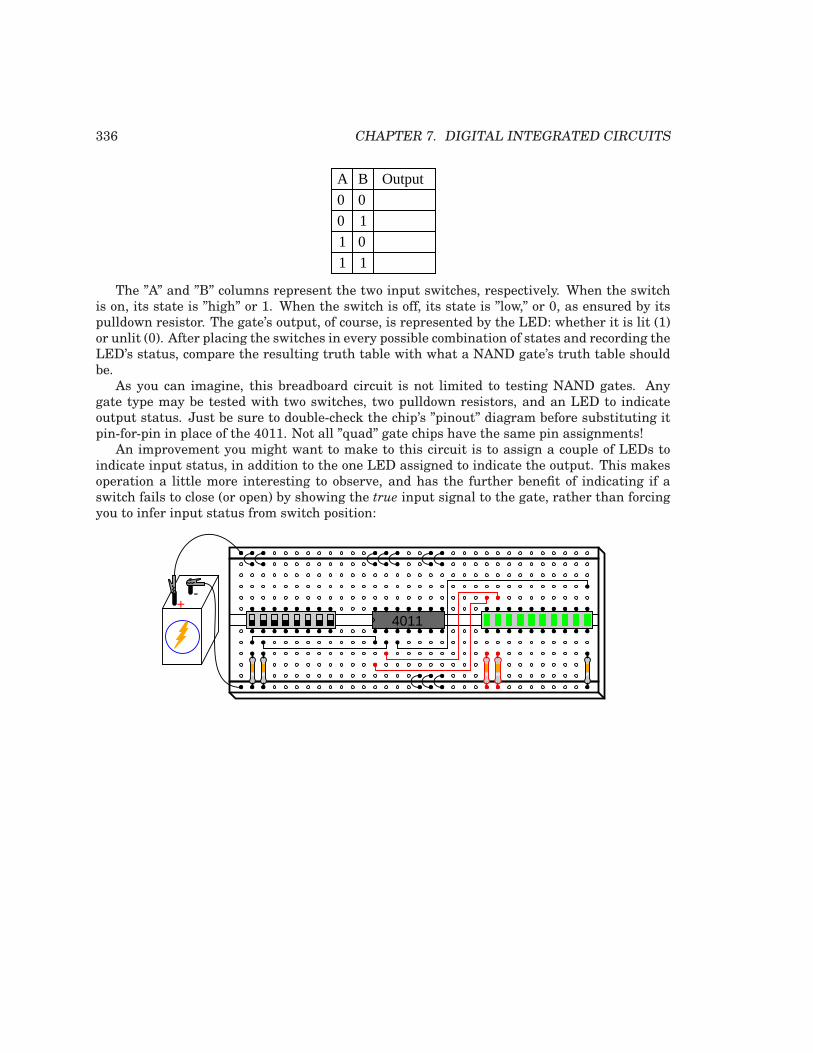
336 CHAPTER 7. DIGITAL INTEGRATED CIRCUITS
A B Output
00
0 1
01
1 1
The ”A” and ”B” columns represent the two input switches, respectively. When the switchis on, its state is ”high” or 1. When the switch is off, its state is ”low,” or 0, as ensured by itspulldown resistor. The gate’s output, of course, is represented by the LED: whether it is lit (1)or unlit (0). After placing the switches in every possible combination of states and recording theLED’s status, compare the resulting truth table with what a NAND gate’s truth table shouldbe.
As you can imagine, this breadboard circuit is not limited to testing NAND gates. Anygate type may be tested with two switches, two pulldown resistors, and an LED to indicateoutput status. Just be sure to double-check the chip’s ”pinout” diagram before substituting itpin-for-pin in place of the 4011. Not all ”quad” gate chips have the same pin assignments!
An improvement you might want to make to this circuit is to assign a couple of LEDs toindicate input status, in addition to the one LED assigned to indicate the output. This makesoperation a little more interesting to observe, and has the further benefit of indicating if aswitch fails to close (or open) by showing the true input signal to the gate, rather than forcingyou to infer input status from switch position:
+-
4011

7.3. NOR GATE S-R LATCH 337
7.3 NOR gate S-R latch
PARTS AND MATERIALS
• 4001 quad NOR gate (Radio Shack catalog # 276-2401)
• Eight-position DIP switch (Radio Shack catalog # 275-1301)
• Ten-segment bargraph LED (Radio Shack catalog # 276-081)
• One 6 volt battery
• Two 10 kΩ resistors
• Two 470 Ω resistors
• Two 100 Ω resistors
Caution! The 4001 IC is CMOS, and therefore sensitive to static electricity!
CROSS-REFERENCES
Lessons In Electric Circuits, Volume 4, chapter 3: ”Logic Gates”Lessons In Electric Circuits, Volume 4, chapter 10: ”Multivibrators”
LEARNING OBJECTIVES
• The effects of positive feedback in a digital circuit
• What is meant by the ”invalid” state of a latch circuit
• What a race condition is in a digital circuit
• The importance of valid ”high” CMOS signal voltage levels
SCHEMATIC DIAGRAM
6 V
1/4 4001
1/4 400110kΩ
470Ω
ILLUSTRATION

338 CHAPTER 7. DIGITAL INTEGRATED CIRCUITS
+-
4001
INSTRUCTIONS
The 4001 integrated circuit is a CMOS quad NOR gate, identical in input, output, andpower supply pin assignments to the 4011 quad NAND gate. Its ”pinout,” or ”connection,”diagram is as such:
14 13 12 11 10 9 8
7654321
VDD
Gnd
"Pinout," or "connection" diagram forthe 4001 quad NOR gate
When two NOR gates are cross-connected as shown in the schematic diagram, there will bepositive feedback from output to input. That is, the output signal tends to maintain the gatein its last output state. Just as in op-amp circuits, positive feedback creates hysteresis. Thistendency for the circuit to remain in its last output state gives it a sort of ”memory.” In fact,there are solid-state computer memory technologies based on circuitry like this!
If we designate the left switch as the ”Set” input and the right switch as the ”Reset,” the leftLED will be the ”Q” output and the right LED the ”Q-not” output. With the Set input ”high”(switch on) and the Reset input ”low,” Q will go ”high” and Q-not will go ”low.” This is knownas the set state of the circuit. Making the Reset input ”high” and the Set input ”low” reversesthe latch circuit’s output state: Q ”low” and Q-not ”high.” This is known as the reset state ofthe circuit. If both inputs are placed into the ”low” state, the circuit’s Q and Q-not outputs willremain in their last states, ”remembering” their prior settings. This is known as the latched
state of the circuit.
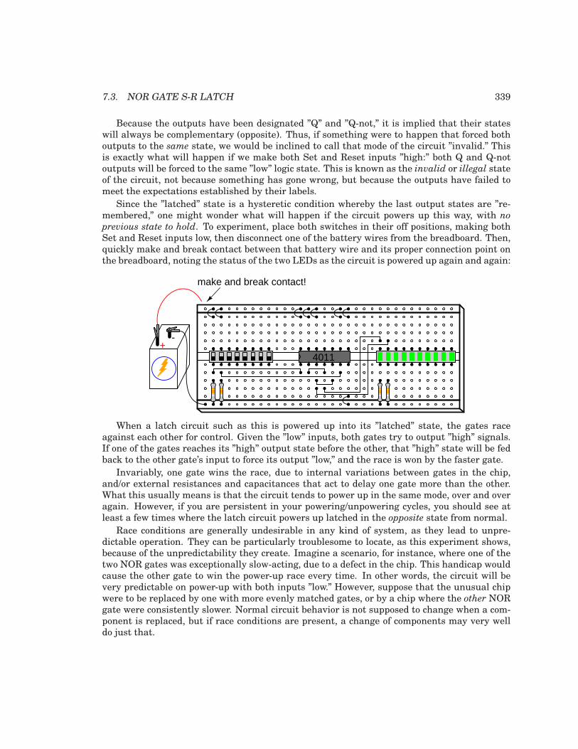
7.3. NOR GATE S-R LATCH 339
Because the outputs have been designated ”Q” and ”Q-not,” it is implied that their stateswill always be complementary (opposite). Thus, if something were to happen that forced bothoutputs to the same state, we would be inclined to call that mode of the circuit ”invalid.” Thisis exactly what will happen if we make both Set and Reset inputs ”high:” both Q and Q-notoutputs will be forced to the same ”low” logic state. This is known as the invalid or illegal stateof the circuit, not because something has gone wrong, but because the outputs have failed tomeet the expectations established by their labels.
Since the ”latched” state is a hysteretic condition whereby the last output states are ”re-membered,” one might wonder what will happen if the circuit powers up this way, with no
previous state to hold. To experiment, place both switches in their off positions, making bothSet and Reset inputs low, then disconnect one of the battery wires from the breadboard. Then,quickly make and break contact between that battery wire and its proper connection point onthe breadboard, noting the status of the two LEDs as the circuit is powered up again and again:
+-
4011
make and break contact!
When a latch circuit such as this is powered up into its ”latched” state, the gates raceagainst each other for control. Given the ”low” inputs, both gates try to output ”high” signals.If one of the gates reaches its ”high” output state before the other, that ”high” state will be fedback to the other gate’s input to force its output ”low,” and the race is won by the faster gate.
Invariably, one gate wins the race, due to internal variations between gates in the chip,and/or external resistances and capacitances that act to delay one gate more than the other.What this usually means is that the circuit tends to power up in the same mode, over and overagain. However, if you are persistent in your powering/unpowering cycles, you should see atleast a few times where the latch circuit powers up latched in the opposite state from normal.
Race conditions are generally undesirable in any kind of system, as they lead to unpre-dictable operation. They can be particularly troublesome to locate, as this experiment shows,because of the unpredictability they create. Imagine a scenario, for instance, where one of thetwo NOR gates was exceptionally slow-acting, due to a defect in the chip. This handicap wouldcause the other gate to win the power-up race every time. In other words, the circuit will bevery predictable on power-up with both inputs ”low.” However, suppose that the unusual chipwere to be replaced by one with more evenly matched gates, or by a chip where the other NORgate were consistently slower. Normal circuit behavior is not supposed to change when a com-ponent is replaced, but if race conditions are present, a change of components may very welldo just that.

340 CHAPTER 7. DIGITAL INTEGRATED CIRCUITS
Due to the inherent race tendency of an S-R latch, one should not design a circuit with theexpectation of a consistent power-up state, but rather use external means to ”force” the race sothat the desired gate always ”wins.”
An interesting modification to try in this circuit is to replace one of the 470 Ω LED ”drop-ping” resistors with a lower-value unit, such as 100 Ω. The obvious effect of this alteration willbe increased LED brightness, as more current is allowed through. A not-so-obvious effect willalso result, and it is this effect which holds great learning value. Try replacing one of the 470 Ω
resistors with a 100 Ω resistor, and operate the input signal switches through all four possiblesetting combinations, noting the behavior of the circuit.
You should note that the circuit refuses to latch in one of its states (either Set or Reset), butonly in the other state, when the input switches are both set ”low” (the ”latch” mode). Why isthis? Take a voltmeter and measure the output voltage of the gate whose output is ”high” whenboth inputs are ”low.” Note this voltage indication, then set the input switches in such a waythat the other state (either Reset or Set) is forced, and measure the output voltage of the othergate when its output is ”high.” Note the difference between the two gate output voltage levels,one gate loaded by an LED with a 470 Ω resistor, and the other loaded by an LED with a 100 Ω
resistor. The one loaded down by the ”heavier” load (100 Ω resistor) will be much less: so muchless that this voltage will not be interpreted by the other NOR gate’s input as a ”high” signalat all as it is fed back! All logic gates have permissible ”high” and ”low” input signal voltageranges, and if the voltage of a digital signal falls outside this permissible range, it might notbe properly interpreted by the receiving gate. In a latch circuit such as this, which depends ona solid ”high” signal fed back from the output of one gate to the input of the other, a ”weak”signal will not be able to maintain the positive feedback necessary to keep the circuit latchedin one of its states.
This is one reason I favor the use of a voltmeter as a logic ”probe” for determining digitalsignal levels, rather than an actual logic probe with ”high” and ”low” lights. A logic probe maynot indicate the presence of a ”weak” signal, whereas a voltmeter definitely will by means ofits quantitative indication. This type of problem, common in circuits where different ”families”of integrated circuits are mixed (TTL and CMOS, for example), can only be found with testequipment providing quantitative measurements of signal level.

7.4. NAND GATE S-R ENABLED LATCH 341
7.4 NAND gate S-R enabled latch
PARTS AND MATERIALS
• 4011 quad NAND gate (Radio Shack catalog # 276-2411)
• Eight-position DIP switch (Radio Shack catalog # 275-1301)
• Ten-segment bargraph LED (Radio Shack catalog # 276-081)
• One 6 volt battery
• Three 10 kΩ resistors
• Two 470 Ω resistors
Caution! The 4011 IC is CMOS, and therefore sensitive to static electricity!
CROSS-REFERENCES
Lessons In Electric Circuits, Volume 4, chapter 3: ”Logic Gates”
Lessons In Electric Circuits, Volume 4, chapter 10: ”Multivibrators”
LEARNING OBJECTIVES
• Principle and function of an enabled latch circuit
SCHEMATIC DIAGRAM
6 V
10kΩ
470Ω
Set Enable Reset
10kΩ
Q Q1/4 4011
1/4 4011
1/4 40111/4 4011
(power connections to gates notshown for simplicity)
ILLUSTRATION

342 CHAPTER 7. DIGITAL INTEGRATED CIRCUITS
+-
4011
INSTRUCTIONS
Although this circuit uses NAND gates instead of NOR gates, its behavior is identical tothat of the NOR gate S-R latch (a ”high” Set input drives Q ”high,” and a ”high” Reset inputdrives Q-not ”high”), except for the presence of a third input: the Enable. The purpose ofthe Enable input is to enable or disable the Set and Reset inputs from having effect over thecircuit’s output status. When the Enable input is ”high,” the circuit acts just like the NOR gateS-R latch. When the Enable input is ”low,” the Set and Reset inputs are disabled and have noeffect whatsoever on the outputs, leaving the circuit in its latched state.
This kind of latch circuit (also called a gated S-R latch), may be constructed from two NORgates and two AND gates, but the NAND gate design is easier to build since it makes use of allfour gates in a single integrated circuit.
R
S
Q
Q
S R
0 0
0
0
1
1
1 1
latch latch
Q Q
0 11 00 0
latch latchlatch latchlatch latchlatch latch0 0
0 1
1 0
1 1
E
0
0
0
0
1
1
1
1
E

7.5. NAND GATE S-R FLIP-FLOP 343
7.5 NAND gate S-R flip-flop
PARTS AND MATERIALS
• 4011 quad NAND gate (Radio Shack catalog # 276-2411)
• 4001 quad NOR gate (Radio Shack catalog # 276-2401)
• Eight-position DIP switch (Radio Shack catalog # 275-1301)
• Ten-segment bargraph LED (Radio Shack catalog # 276-081)
• One 6 volt battery
• Three 10 kΩ resistors
• Two 470 Ω resistors
Caution! The 4011 IC is CMOS, and therefore sensitive to static electricity!
Although the parts list calls for a ten-segment LED unit, the illustration shows two indi-vidual LEDs being used instead. This is due to lack of room on my breadboard to mount theswitch assembly, two integrated circuits, and the bargraph. If you have room on your bread-board, feel free to use the bargraph as called for in the parts list, and as shown in prior latchcircuits.
CROSS-REFERENCES
Lessons In Electric Circuits, Volume 4, chapter 3: ”Logic Gates”
Lessons In Electric Circuits, Volume 4, chapter 10: ”Multivibrators”
LEARNING OBJECTIVES
• The difference between a gated latch and a flip-flop
• How to build a ”pulse detector” circuit
• Learn the effects of switch contact ”bounce” on digital circuits
SCHEMATIC DIAGRAM

344 CHAPTER 7. DIGITAL INTEGRATED CIRCUITS
6 V
10kΩ
470Ω
Set Reset
10kΩ
Q Q1/4 4011
1/4 4011
1/4 40111/4 4011
(power connections to gates notshown for simplicity)Clock
1/4 4001 1/4 4001 1/4 4001
1/4 4001
ILLUSTRATION
+-
40114001
INSTRUCTIONS
The only difference between a gated (or enabled) latch and a flip-flop is that a flip-flop isenabled only on the rising or falling edge of a ”clock” signal, rather than for the entire durationof a ”high” enable signal. Converting an enabled latch into a flip-flop simply requires that a”pulse detector” circuit be added to the Enable input, so that the edge of a clock pulse generatesa brief ”high” Enable pulse:

7.5. NAND GATE S-R FLIP-FLOP 345
InputOutput
Input
Delayed input
Delayed input
Output
Brief period of time when
are lowboth inputs of the NOR gate
The single NOR gate and three inverter gates create this effect by exploiting the propaga-tion delay time of multiple, cascaded gates. In this experiment, I use three NOR gates withparalleled inputs to create three inverters, thus using all four NOR gates of a 4001 integratedcircuit:
InputOutput
Pulse detector circuit
1/4 4001 1/4 4001 1/4 4001
1/4 4001
Normally, when using a NOR gate as an inverter, one input would be grounded while theother acts as the inverter input, to minimize input capacitance and increase speed. Here,however, slow response is desired, and so I parallel the NOR inputs to make inverters ratherthan use the more conventional method.
Please note that this particular pulse detector circuit produces a ”high” output pulse atevery falling edge of the clock (input) signal. This means that the flip-flop circuit should beresponsive to the Set and Reset input states only when the middle switch is moved from ”on”to ”off,” not from ”off” to ”on.”
When you build this circuit, though, you may discover that the outputs respond to Set andReset input signals during both transitions of the Clock input, not just when it is switched froma ”high” state to a ”low” state. The reason for this is contact bounce: the effect of a mechan-ical switch rapidly making-and-breaking when its contacts are first closed, due to the elasticcollision of the metal contact pads. Instead of the Clock switch producing a single, clean low-to-high signal transition when closed, there will most likely be several low-high-low ”cycles”as the contact pads ”bounce” upon off-to-on actuation. The first high-to-low transition causedby bouncing will trigger the pulse detector circuit, enabling the S-R latch for that moment intime, making it responsive to the Set and Reset inputs.
Ideally, of course, switches are perfect and bounce-free. In the real world, though, contactbounce is a very common problem for digital gate circuits operated by switch inputs, and must

346 CHAPTER 7. DIGITAL INTEGRATED CIRCUITS
be understood well if it is to be overcome.

7.6. LED SEQUENCER 347
7.6 LED sequencer
PARTS AND MATERIALS
• 4017 decade counter/divider (Radio Shack catalog # 276-2417)
• 555 timer IC (Radio Shack catalog # 276-1723)
• Ten-segment bargraph LED (Radio Shack catalog # 276-081)
• One SPST switch
• One 6 volt battery
• 10 kΩ resistor
• 1 MΩ resistor
• 0.1 µF capacitor (Radio Shack catalog # 272-135 or equivalent)
• Coupling capacitor, 0.047 to 0.001 µF
• Ten 470 Ω resistors
• Audio detector with headphones
Caution! The 4017 IC is CMOS, and therefore sensitive to static electricity!Any single-pole, single-throw switch is adequate. A household light switch will work fine,
and is readily available at any hardware store.The audio detector will be used to assess signal frequency. If you have access to an oscillo-
scope, the audio detector is unnecessary.
CROSS-REFERENCES
Lessons In Electric Circuits, Volume 4, chapter 3: ”Logic Gates”Lessons In Electric Circuits, Volume 4, chapter 4: ”Switches”Lessons In Electric Circuits, Volume 4, chapter 11: ”Counters”
LEARNING OBJECTIVES
• Use of a 555 timer circuit to produce ”clock” pulses (astable multivibrator)
• Use of a 4017 decade counter/divider circuit to produce a sequence of pulses
• Use of a 4017 decade counter/divider circuit for frequency division
• Using a frequency divider and timepiece (watch) to measure frequency
• Purpose of a ”pulldown” resistor
• Learn the effects of switch contact ”bounce” on digital circuits
• Use of a 555 timer circuit to ”debounce” a mechanical switch (monostable multivibrator)

348 CHAPTER 7. DIGITAL INTEGRATED CIRCUITS
SCHEMATIC DIAGRAM
Ten-segmentLED bargraph
470 Ω each
555Disch
Thresh
Trig
Gnd
Vcc RST
Out
Ctrl
1 MΩ
0.1 µF
0 1 2 3 4 5 6 7 8 9
VDD 4017
Clk
Gnd
ClkEn Rst Carry
6 V
ILLUSTRATION
+-
555 4017
INSTRUCTIONS
The model 4017 integrated circuit is a CMOS counter with ten output terminals. One ofthese ten terminals will be in a ”high” state at any given time, with all others being ”low,”giving a ”one-of-ten” output sequence. If low-to-high voltage pulses are applied to the ”clock”(Clk) terminal of the 4017, it will increment its count, forcing the next output into a ”high”state.
With a 555 timer connected as an astable multivibrator (oscillator) of low frequency, the4017 will cycle through its ten-count sequence, lighting up each LED, one at a time, and ”recy-cling” back to the first LED. The result is a visually pleasing sequence of flashing lights. Feelfree to experiment with resistor and capacitor values on the 555 timer to create different flashrates.
Try disconnecting the jumper wire leading from the 4017’s ”Clock” terminal (pin #14) to the555’s ”Output” terminal (pin #3) where it connects to the 555 timer chip, and hold its end inyour hand. If there is sufficient 60 Hz power-line ”noise” around you, the 4017 will detect it asa fast clock signal, causing the LEDs to blink very rapidly.
Two terminals on the 4017 chip, ”Reset” and ”Clock Enable,” are maintained in a ”low” stateby means of a connection to the negative side of the battery (ground). This is necessary if thechip is to count freely. If the ”Reset” terminal is made ”high,” the 4017’s output will be reset

7.6. LED SEQUENCER 349
back to 0 (pin #3 ”high,” all other output pins ”low”). If the ”Clock Enable” is made ”high,” thechip will stop responding to the clock signal and pause in its counting sequence.
If the 4017’s ”Reset” terminal is connected to one of its ten output terminals, its countingsequence will be cut short, or truncated. You may experiment with this by disconnecting the”Reset” terminal from ground, then connecting a long jumper wire to the ”Reset” terminal foreasy connection to the outputs at the ten-segment LED bargraph. Notice how many (or howfew) LEDs light up with the ”Reset” connected to any one of the outputs:
+-
555 4017
disconnect
touch end of long jumper wireto an LED terminal
Counters such as the 4017 may be used as digital frequency dividers, to take a clock signaland produce a pulse occurring at some integer factor of the clock frequency. For example, if theclock signal from the 555 timer is 200 Hz, and the 4017 is configured for a full-count sequence(the ”Reset” terminal connected to ground, giving a full, ten-step count), a signal with a periodten times as long (20 Hz) will be present at any of the 4017’s output terminals. In other words,each output terminal will cycle once for every ten cycles of the clock signal: a frequency tentimes as slow.
To experiment with this principle, connect your audio detector between output 0 (pin #3) ofthe 4017 and ground, through a very small capacitor (0.047 µF to 0.001 µF). The capacitor isused for ”coupling” AC signals only, to that you may audibly detect pulses without placing aDC (resistive) load on the counter chip output. With the 4017 ”Reset” terminal grounded, youwill have a full-count sequence, and you will hear a ”click” in the headphones every time the”0” LED lights up, corresponding to 1/10 of the 555’s actual output frequency:

350 CHAPTER 7. DIGITAL INTEGRATED CIRCUITS
+-
555 4017
plug
headphones
Sensitivity
In fact, knowing this mathematical relationship between clicks heard in the headphoneand the clock frequency allows us to measure the clock frequency to a fair degree of precision.Using a stopwatch or other timepiece, count the number of clicks heard in one full minutewhile connected to the 4017’s ”0” output. Using a 1 MΩ resistor and 0.1 µF capacitor in the555 timing circuit, and a power supply voltage of 13 volts (instead of 6), I counted 79 clicks inone minute from my circuit. Your circuit may produce slightly different results. Multiply thenumber of pulses counted at the ”0” output by 10 to obtain the number of cycles produced bythe 555 timer during that same time (my circuit: 79 x 10 = 790 cycles). Divide this numberby 60 to obtain the number of timer cycles elapsed in each second (my circuit: 790/60 = 13.17).This final figure is the clock frequency in Hz.
Now, leaving one test probe of the audio detector connected to ground, take the other testprobe (the one with the coupling capacitor connected in series) and connect it to pin #3 of the555 timer. The buzzing you hear is the undivided clock frequency:
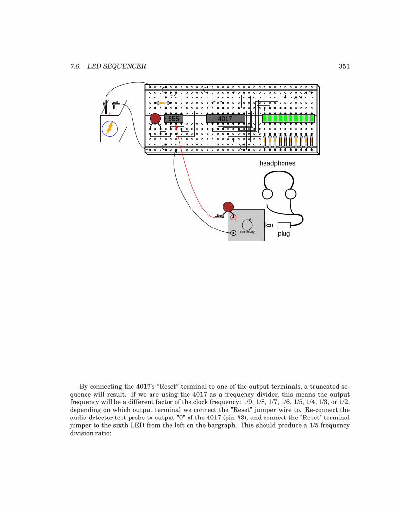
7.6. LED SEQUENCER 351
+-
555 4017
plug
headphones
Sensitivity
By connecting the 4017’s ”Reset” terminal to one of the output terminals, a truncated se-quence will result. If we are using the 4017 as a frequency divider, this means the outputfrequency will be a different factor of the clock frequency: 1/9, 1/8, 1/7, 1/6, 1/5, 1/4, 1/3, or 1/2,depending on which output terminal we connect the ”Reset” jumper wire to. Re-connect theaudio detector test probe to output ”0” of the 4017 (pin #3), and connect the ”Reset” terminaljumper to the sixth LED from the left on the bargraph. This should produce a 1/5 frequencydivision ratio:
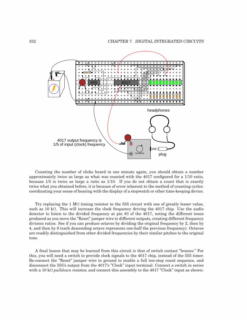
352 CHAPTER 7. DIGITAL INTEGRATED CIRCUITS
+-
555 4017
plug
headphones
Sensitivity
4017 output frequency is1/5 of input (clock) frequency
Counting the number of clicks heard in one minute again, you should obtain a numberapproximately twice as large as what was counted with the 4017 configured for a 1/10 ratio,because 1/5 is twice as large a ratio as 1/10. If you do not obtain a count that is exactlytwice what you obtained before, it is because of error inherent to the method of counting cycles:coordinating your sense of hearing with the display of a stopwatch or other time-keeping device.
Try replacing the 1 MΩ timing resistor in the 555 circuit with one of greatly lesser value,such as 10 kΩ. This will increase the clock frequency driving the 4017 chip. Use the audiodetector to listen to the divided frequency at pin #3 of the 4017, noting the different tonesproduced as you move the ”Reset” jumper wire to different outputs, creating different frequencydivision ratios. See if you can produce octaves by dividing the original frequency by 2, then by4, and then by 8 (each descending octave represents one-half the previous frequency). Octavesare readily distinguished from other divided frequencies by their similar pitches to the originaltone.
A final lesson that may be learned from this circuit is that of switch contact ”bounce.” Forthis, you will need a switch to provide clock signals to the 4017 chip, instead of the 555 timer.Re-connect the ”Reset” jumper wire to ground to enable a full ten-step count sequence, anddisconnect the 555’s output from the 4017’s ”Clock” input terminal. Connect a switch in serieswith a 10 kΩ pulldown resistor, and connect this assembly to the 4017 ”Clock” input as shown:

7.6. LED SEQUENCER 353
Ten-segmentLED bargraph
470 Ω each
0 1 2 3 4 5 6 7 8 9
VDD 4017
Clk
Gnd
ClkEn Rst Carry
6 V
10 kΩ
+-
555 4017
disconnect
connect
conn
ect
connect
The purpose of a ”pulldown” resistor is to provide a definite ”low” logic state when the switchcontact opens. Without this resistor in place, the 4017’s ”Clock” input wire would be floating
whenever the switch contact was opened, leaving it susceptible to interference from stray staticvoltages or electrical ”noise,” either one capable of making the 4017 count randomly. Withthe pulldown resistor in place, the 4017’s ”Clock” input will have a definite, albeit resistive,connection to ground, providing a stable ”low” logic state that precludes any interference fromstatic electricity or ”noise” coupled from nearby AC circuit wiring.
Actuate the switch on and off, noting the action of the LEDs. With each off-to-on switchtransition, the 4017 should increment once in its count. However, you may notice some strangebehavior: sometimes, the LED sequence will ”skip” one or even several steps with a singleswitch closure. Why is this? It is due to very rapid, mechanical ”bouncing” of the switchcontacts. When two metallic contacts are brought together rapidly as does happen inside mostswitches, there will be an elastic collision. This collision results in the contacts making andbreaking very rapidly as they ”bounce” off one another. Normally, this ”bouncing” is much torapid for you to see its effects, but in a digital circuit such as this where the counter chip is able

354 CHAPTER 7. DIGITAL INTEGRATED CIRCUITS
to respond to very quick clock pulses, these ”bounces” are interpreted as distinct clock signals,and the count incremented accordingly.
One way to combat this problem is to use a timing circuit to produce a single pulse for anynumber of input pulse signals received within a short amount of time. The circuit is calleda monostable multivibrator, and any technique eliminating the false pulses caused by switchcontact ”bounce” is called debouncing.
The 555 timer circuit is capable of functioning as a debouncer, if the ”Trigger” input isconnected to the switch as such:
555Disch
Thresh
Trig
Gnd
Vcc RST
Out
Ctrl
1 MΩ
0.1 µF
0 1 2 3 4 5 6 7 8 9
VDD 4017
Clk
Gnd
ClkEn Rst Carry
6 V
10 kΩ
Using the 555 timer to "debounce" the switch
+-
555 4017
Please note that since we are using the 555 once again to provide a clock signal to the 4017,we must re-connect pin #3 of the 555 chip to pin #14 of the 4017 chip! Also, if you have alteredthe values of the resistor or capacitor in the 555 timer circuit, you should return to the original1 MΩ and 0.1 µF components.
Actuate the switch again and note the counting behavior of the 4017. There should beno more ”skipped” counts as there were before, because the 555 timer outputs a single, crisppulse for every on-to-off actuation (notice the inversion of operation here!) of the switch. It is

7.6. LED SEQUENCER 355
important that the timing of the 555 circuit be appropriate: the time to charge the capacitorshould be longer than the ”settling” period of the switch (the time required for the contactsto stop bouncing), but not so long that the timer would ”miss” a rapid sequence of switchactuations, if they were to occur.

356 CHAPTER 7. DIGITAL INTEGRATED CIRCUITS
7.7 Simple combination lock
PARTS AND MATERIALS
• 4001 quad NOR gate (Radio Shack catalog # 276-2401)
• 4070 quad XOR gate (Radio Shack catalog # 900-6906)
• Two, eight-position DIP switches (Radio Shack catalog # 275-1301)
• Two light-emitting diodes (Radio Shack catalog # 276-026 or equivalent)
• Four 1N914 ”switching” diodes (Radio Shack catalog # 276-1122)
• Ten 10 kΩ resistors
• Two 470 Ω resistors
• Pushbutton switch, normally open (Radio Shack catalog # 275-1556)
• Two 6 volt batteries
Caution! Both the 4001 and 4070 ICs are CMOS, and therefore sensitive to static electric-ity!
This experiment may be built using only one 8-position DIP switch, but the concept is easierto understand if two switch assemblies are used. The idea is, one switch acts to hold the correctcode for unlocking the lock, while the other switch serves as a data entry point for the persontrying to open the lock. In real life, of course, the switch assembly with the ”key” code seton it must be hidden from the sight of the person opening the lock, which means it must bephysically located elsewhere from where the data entry switch assembly is. This requires twoswitch assemblies. However, if you understand this concept clearly, you may build a workingcircuit with only one 8-position switch, using the left four switches for data entry and the rightfour switches to hold the ”key” code.
For extra effect, choose different colors of LED: green for ”Go” and red for ”No go.”
CROSS-REFERENCES
Lessons In Electric Circuits, Volume 4, chapter 3: ”Logic Gates”
LEARNING OBJECTIVES
• Using XOR gates as bit comparators
• How to build simple gate functions with diodes and a pullup/down resistor
• Using NOR gates as controlled inverters
SCHEMATIC DIAGRAM

7.7. SIMPLE COMBINATION LOCK 357
10 kΩ
Vdd
Vdd
10 kΩ(all)
Vdd
10 kΩ(all)
switch
Data entryswitch
"Key code"
Enter
470 Ω
470 Ω
Go
No go
10 kΩ
ILLUSTRATION
+-
+-
4070 4001
Enter
Data entry
"Key" code
INSTRUCTIONS
This circuit illustrates the use of XOR (Exclusive-OR) gates as bit comparators. Four ofthese XOR gates compare the respective bits of two 4-bit binary numbers, each number ”en-tered” into the circuit via a set of switches. If the two numbers match, bit for bit, the green”Go” LED will light up when the ”Enter” pushbutton switch is pressed. If the two numbers donot exactly match, the red ”No go” LED will light up when the ”Enter” pushbutton is pressed.

358 CHAPTER 7. DIGITAL INTEGRATED CIRCUITS
Because four bits provides a mere sixteen possible combinations, this lock circuit is not verysophisticated. If it were used in a real application such as a home security system, the ”No go”output would have to be connected to some kind of siren or other alarming device, so that theentry of an incorrect code would deter an unauthorized person from attempting another codeentry. Otherwise, it would not take much time to try all combinations (0000 through 1111)until the correct one was found! In this experiment, I do not describe how to work this circuitinto a real security system or lock mechanism, but only how to make it recognize a pre-enteredcode.
The ”key” code that must be matched at the data entry switch array should be hidden fromview, of course. If this were part of a real security system, the data entry switch assemblywould be located outside the door, and the key code switch assembly behind the door with therest of the circuitry. In this experiment, you will likely locate the two switch assemblies ontwo different breadboards, but it is entirely possible to build the circuit using just a single(8-position) DIP switch assembly. Again, the purpose of the experiment is not to make a realsecurity system, but merely to introduce you to the principle of XOR gate code comparison.
It is the nature of an XOR gate to output a ”high” (1) signal if the input signals are not thesame logic state. The four XOR gates’ output terminals are connected through a diode networkwhich functions as a four-input OR gate: if any of the four XOR gates outputs a ”high” signal –indicating that the entered code and the key code are not identical – then a ”high” signal willbe passed on to the NOR gate logic. If the two 4-bit codes are identical, then none of the XORgate outputs will be ”high,” and the pull-down resistor connected to the common sides of thediodes will provide a ”low” signal state to the NOR logic.
The NOR gate logic performs a simple task: prevent either of the LEDs from turning onif the ”Enter” pushbutton is not pressed. Only when this pushbutton is pressed can either ofthe LEDs energize. If the Enter switch is pressed and the XOR outputs are all ”low,” the ”Go”LED will light up, indicating that the correct code has been entered. If the Enter switch ispressed and any of the XOR outputs are ”high,” the ”No go” LED will light up, indicating thatan incorrect code has been entered. Again, if this were a real security system, it would be wiseto have the ”No go” output do something that deters an unauthorized person from discoveringthe correct code by trial-and-error. In other words, there should be some sort of penalty forentering an incorrect code. Let your imagination guide your design of this detail!

7.8. 3-BIT BINARY COUNTER 359
7.8 3-bit binary counter
PARTS AND MATERIALS
• 555 timer IC (Radio Shack catalog # 276-1723)
• One 1N914 ”switching” diode (Radio Shack catalog # 276-1122)
• Two 10 kΩ resistors
• One 100 µF capacitor (Radio Shack catalog # 272-1028)
• 4027 dual J-K flip-flop (Radio Shack catalog # 900-4394)
• Ten-segment bargraph LED (Radio Shack catalog # 276-081)
• Three 470 Ω resistors
• One 6 volt battery
Caution! The 4027 IC is CMOS, and therefore sensitive to static electricity!
CROSS-REFERENCES
Lessons In Electric Circuits, Volume 4, chapter 10: ”Multivibrators”Lessons In Electric Circuits, Volume 4, chapter 11: ”Counters”
LEARNING OBJECTIVES
• Using the 555 timer as a square-wave oscillator
• How to make an asynchronous counter using J-K flip-flops
SCHEMATIC DIAGRAM
555Disch
Thresh
Trig
Gnd
Vcc RST
Out
Ctrl
0.1 µF
6 V
10 kΩ
10kΩ
J Q
Q
C
K
J Q
Q
C
K
R
S S
R
(LSB) (MSB)
470 Ω 470 Ω 470 Ω

360 CHAPTER 7. DIGITAL INTEGRATED CIRCUITS
ILLUSTRATION
+-
555 4027
INSTRUCTIONS
In a sense, this circuit ”cheats” by using only two J-K flip-flops to make a three-bit binarycounter. Ordinarily, three flip-flops would be used – one for each binary bit – but in this casewe can use the clock pulse (555 timer output) as a bit of its own. When you build this circuit,you will find that it is a ”down” counter. That is, its count sequence goes from 111 to 110 to101 to 100 to 011 to 010 to 001 to 000 and then back to 111. While it is possible to constructan ”up” counter using J-K flip-flops, this would require additional components and introducemore complexity into the circuit.
The 555 timer operates as a slow, square-wave oscillator with a duty cycle of approximately50 percent. This duty cycle is made possible by the use of a diode to ”bypass” the lower resistorduring the capacitor’s charging cycle, so that the charging time constant is only RC and not2RC as it would be without the diode in place.
It is highly recommended, in this experiment as in all experiments, to build the circuit instages: identify portions of the circuit with specific functions, and build those portions one at atime, testing each one and verifying its performance before building the next. A very commonmistake of new electronics students is to build an entire circuit at once without testing sectionsof it during the construction process, and then be faced with the possibility of several problemssimultaneously when it comes time to finally apply power to it. Remember that a small amountof extra attention paid to detail near the beginning of a project is worth an enormous amountof troubleshooting work near the end! Students who make the mistake of not testing circuitportions before attempting to operate the entire circuit often (falsely) think that the time itwould take to test those sections is not worth it, and then spend days trying to figure out whatthe problem(s) might be with their experiment.
Following this philosophy, build the 555 timer circuit first, before even plugging the 4027IC into the breadboard. Connect the 555’s output (pin #3) to the ”Least Significant Bit” (LSB)LED, so that you have visual indication of its status. Make sure that the output oscillates in aslow, square-wave pattern (LED is ”lit” for about as long as it is ”off” in a cycle), and that it isa reliable signal (no erratic behavior, no unexplained pauses). If the 555 timer is not workingproperly, neither will the rest of the counter circuit! Once the timer circuit has been provengood, proceed to plug the 4027 IC into the breadboard and complete the rest of the necessaryconnections between it, the 555 timer circuit, and the LED assembly.

7.9. 7-SEGMENT DISPLAY 361
7.9 7-segment display
PARTS AND MATERIALS
• 4511 BCD-to-7seg latch/decoder/driver (Radio Shack catalog # 900-4437)
• Common-cathode 7-segment LED display (Radio Shack catalog # 276-075)
• Eight-position DIP switch (Radio Shack catalog # 275-1301)
• Four 10 kΩ resistors
• Seven 470 Ω resistors
• One 6 volt battery
Caution! The 4511 IC is CMOS, and therefore sensitive to static electricity!
CROSS-REFERENCES
Lessons In Electric Circuits, Volume 4, chapter 9: ”Combinational Logic Functions”
LEARNING OBJECTIVES
• How to use the 4511 7-segment decoder/display driver IC
• Gain familiarity with the BCD code
• How to use 7-segment LED assemblies to create decimal digit displays
• How to identify and use both ”active-low” and ”active-high” logic inputs
SCHEMATIC DIAGRAM
4511ABCD
VDD
Gnd
abcdefg
LTBI
LECathode
470 Ωeach
a
b
cd
e
fg
(MSB)
(LSB)
10 kΩeach6 V

362 CHAPTER 7. DIGITAL INTEGRATED CIRCUITS
ILLUSTRATION
+-
4511
INSTRUCTIONS
This experiment is more of an introduction to the 4511 decoder/display driver IC than it isa lesson in how to ”build up” a digital function from lower-level components. Since 7-segmentdisplays are very common components of digital devices, it is good to be familiar with the”driving” circuits behind them, and the 4511 is a good example of a typical driver IC.
Its operating principle is to input a four-bit BCD (Binary-Coded Decimal) value, and en-ergize the proper output lines to form the corresponding decimal digit on the 7-segment LEDdisplay. The BCD inputs are designated A, B, C, and D in order from least-significant to most-significant. Outputs are labeled a, b, c, d, e, f, and g, each letter corresponding to a standardizedsegment designation for 7-segment displays. Of course, since each LED segment requires itsown dropping resistor, we must use seven 470 Ω resistors placed in series between the 4511’soutput terminals and the corresponding terminals of the display unit.
Most 7-segment displays also provide for a decimal point (sometimes two!), a separate LEDand terminal designated for its operation. All LEDs inside the display unit are made commonto each other on one side, either cathode or anode. The 4511 display driver IC requires acommon-cathode 7-segment display unit, and so that is what is used here.
After building the circuit and applying power, operate the four switches in a binary countingsequence (0000 to 1111), noting the 7-segment display. A 0000 input should result in a decimal”0” display, a 0001 input should result in a decimal ”1” display, and so on through 1001 (decimal”9”). What happens for the binary numbers 1010 (10) through 1111 (15)? Read the datasheeton the 4511 IC and see what the manufacturer specifies for operation above an input value of9. In the BCD code, there is no real meaning for 1010, 1011, 1100, 1101, 1110, or 1111. Theseare binary values beyond the range of a single decimal digit, and so have no function in a BCDsystem. The 4511 IC is built to recognize this, and output (or not output!) accordingly.
Three inputs on the 4511 chip have been permanently connected to either Vdd or ground:the ”Lamp Test,” ”Blanking Input,” and ”Latch Enable.” To learn what these inputs do, removethe short jumpers connecting them to either power supply rail (one at a time!), and replacethe short jumper with a longer one that can reach the other power supply rail. For example,remove the short jumper connecting the ”Latch Enable” input (pin #5) to ground, and replaceit with a long jumper wire that can reach all the way to the Vdd power supply rail. Experimentwith making this input ”high” and ”low,” observing the results on the 7-segment display as youalter the BCD code with the four input switches. After you’ve learned what the input’s function

7.9. 7-SEGMENT DISPLAY 363
is, connect it to the power supply rail enabling normal operation, and proceed to experimentwith the next input (either ”Lamp Test” or ”Blanking Input”).
Once again, the manufacturer’s datasheet will be informative as to the purpose of each ofthese three inputs. Note that the ”Lamp Test” (LT) and ”Blanking Input” (BI) input labelsare written with boolean complementation bars over the abbreviations. Bar symbols designatethese inputs as active-low, meaning that you must make each one ”low” in order to invokeits particular function. Making an active-low input ”high” places that particular input into a”passive” state where its function will not be invoked. Conversely, the ”Latch Enable” (LE)input has no complementation bar written over its abbreviation, and correspondingly it isshown connected to ground (”low”) in the schematic so as to not invoke that function. The”Latch Enable” input is an active-high input, which means it must be made ”high” (connectedto Vdd) in order to invoke its function.

364 CHAPTER 7. DIGITAL INTEGRATED CIRCUITS

Chapter 8
555 TIMER CIRCUITS
Contents
8.1 The 555 IC . . . . . . . . . . . . . . . . . . . . . . . . . . . . . . . . . . . . . . . 365
8.2 555 Schmitt Trigger . . . . . . . . . . . . . . . . . . . . . . . . . . . . . . . . . 366
8.3 555 HYSTERETIC OSCILLATOR . . . . . . . . . . . . . . . . . . . . . . . . . 370
8.4 555 MONOSTABLE MULTIVIBRATOR . . . . . . . . . . . . . . . . . . . . . . 374
8.5 CMOS 555 LONG DURATION MINIMUM PARTS RED LED FLASHER . 380
8.6 CMOS 555 LONG DURATION BLUE LED FLASHER . . . . . . . . . . . . . 385
8.7 CMOS 555 LONG DURATION FLYBACK LED FLASHER . . . . . . . . . . 389
8.8 HOW TO MAKE AN INDUCTOR . . . . . . . . . . . . . . . . . . . . . . . . . . 392
8.9 CMOS 555 LONG DURATION RED LED FLASHER . . . . . . . . . . . . . . 395
Original author: Bill Marsden
8.1 The 555 IC
The 555 integrated circuit is the most popular chip ever manufactured. Independently manu-factured by more than 10 manufacturers, still in current production, and almost 40 years old,this little circuit has withstood the test of time. It has been redesigned, improved, and recon-figured in many ways, yet the original design can be bought from many vendors. The design ofthis chip was right the first time.
Originally conceived in 1970 and created by Hans R. Camenzind in 1971, over 1 billionof these ICs were made in 2003 with no apparent reduction in demand. It has been used ineverything from toys to spacecraft. Due to its versatility, availability, and low cost it remains ahobbyist favorite.
One of the secrets to its success is it is a true black box, its symbolized schematic is simpleand accurate enough that designs using this simplification as a reference tend to work firsttime. You don’t need to understand every transistor in the base schematic to make it work.
365

366 CHAPTER 8. 555 TIMER CIRCUITS
It has been used to derive the 556, a dual 555, each independent of the other in one 14pin package, and is the inspiration of the 558, a quad timer in a 16 pin package. What fewweak points the original design has have been addressed by redesigns into CMOS technology,with its dramatically reduced current and expanded voltage requirements, and yet the originalversion remains.
Originally conceived as a simple timer, the 555 has been used for oscillators, waveformgenerators, VCO’s, FM discrimination, and a lot more. It really is an all purpose circuit.
SOURCES
• The 555 Timer IC - An Interview with Hans Camenzind ( http://semiconductormuseum.com/Transistors/LectureHall/Camenzind/Camenzind Index.htm )
• 555 Tutorial ( http://www.sentex.ca/˜mec1995/gadgets/555/555.html )
• 555 Timer IC Encyclopedia Article ( http://www.nationmaster.com/encyclopedia/555-timer-IC )
8.2 555 Schmitt Trigger
PARTS AND MATERIALS
• One 9V Battery
• Battery Clip (Radio Shack catalog # 270-325)
• Mini Hook Clips (soldered to Battery Clip, Radio Shack catalog # 270-372)
• One Potentiometer, 10 KΩ, 15-Turn (Radio Shack catalog # 271-343)
• One 555 timer IC (Radio Shack catalog # 276-1723)
• One red light-emitting diode (Radio Shack catalog # 276-041 or equivalent)
• One green light-emitting diode (Radio Shack catalog # 276-022 or equivalent)
• Two 1 KΩ Resistors
• One DVM (Digital Volt Meter) or VOM (Volt Ohm Meter)
CROSS-REFERENCES
Lessons In Electric Circuits, Volume 3, chapter 8: “Positive Feedback”Lessons In Electric Circuits, Volume 4, chapter 3: “Logic Signal Voltage Levels”
LEARNING OBJECTIVES
• Learn how a Schmitt Trigger works
• How to use the 555 timer as an Schmitt Trigger

8.2. 555 SCHMITT TRIGGER 367
SCHEMATIC DIAGRAM
Schmitt Triggers have a convention to show a gate that is also a Schmitt Trigger, shownbelow.
The same schematic redrawn to reflect this convention looks something like this:
ILLUSTRATION

368 CHAPTER 8. 555 TIMER CIRCUITS
INSTRUCTIONS
The 555 timer is probably one of the more versatile ”black box” chips. Its 3 resistor voltagedivider, 2 comparators, and built in set reset flip flop are wired to form a Schmitt Trigger in thisdesign. Its interesting to note that the configuration isnt even close to the op amp configurationshown elsewhere, but the end result is identical.
Try adjusting the potentiometer until the lights flip states, then measure the voltage. Com-pare this voltage to the power supply voltage. Adjust the potentiometer the other way untilthe LEDs flip states again, and measure the voltage. How close to the 1/3 and 2/3 marks didyou get?
Try substituting the 9V battery with a 6 volt battery, or two 6 volt batteries, and see howclose the thresholds are to the 1/3 and 2/3 marks.
Schmitt Triggers are a fundamental circuit with several uses. One is signal processing,they can pull digital data out of some extremely noisy environments. Other big uses will beshown in following projects, such as an extremely simple RC oscillator.
THEORY OF OPERATION
The defining characteristic of any Schmitt Trigger is its hysteresis. In this case it is 1/3 and2/3 of the power supply voltage, defined by the built in resistor voltage divider on the 555. Thebuilt in comparators C1 and C2 compare the input voltage to the references provided by thevoltage divider and use the comparison to trip the built in flip flop, which drives the outputdriver, another nice feature of the 555. The 555 can drive up to 200ma off either side of thepower supply rail, the output driver creates a very low conduction path to either side of thepower supply connections. The circuit ”shorts” each side of the LED circuit, leaving the otherside to light up.

8.2. 555 SCHMITT TRIGGER 369
The 5KΩ resistors are not very accurate. It is interesting to note that IC fabrication doesn’tgenerally allow precision resistors, but the resistors compared to each other are extremely closein value, which is critical to the circuit’s operation.

370 CHAPTER 8. 555 TIMER CIRCUITS
8.3 555 HYSTERETIC OSCILLATOR
PARTS AND MATERIALS
• One 9V Battery
• Battery Clip (Radio Shack catalog # 270-325)
• Mini Hook Clips (soldered to Battery Clip, Radio Shack catalog # 270-372)
• U1 - 555 timer IC (Radio Shack catalog # 276-1723)
• D1 - Red light-emitting diode (Radio Shack catalog # 276-041 or equivalent)
• D2 - Green light-emitting diode (Radio Shack catalog # 276-022 or equivalent)
• R1,R2 - 1 KΩ 1/4W Resistors
• R3 - 10 Ω 1/4W Resistor
• R4 - 10 KΩ, 15-Turn Potentiometer (Radio Shack catalog # 271-343)
• C1 - 1 µF Capacitor (Radio Shack catalog 272-1434 or equivalent)
• C1 - 100 µF Capacitor (Radio Shack catalog 272-1028 or equivalent)
CROSS-REFERENCES
Lessons In Electric CircuitsVolume 1, chapter 16: Voltage and current calculations
Lessons In Electric Circuits, Volume 1, chapter 16: Solving for unknown time
Lessons In Electric Circuits, Volume 4, chapter 10: Multivibrators
Lessons in Electric Circuits, Volume 3, chapter 8: Positive Feedback
LEARNING OBJECTIVES
• Learn how to use a Schmitt Trigger for a simple RC Oscillator
• Learn a practical application for a RC time constant
• Learn one of several 555 timer Astable Multivibrator Configurations
SCHEMATIC DIAGRAM
Here is one way of drawing the schematic:

8.3. 555 HYSTERETIC OSCILLATOR 371
As mentioned in the previous experiment, there is also another convention, shown below:
ILLUSTRATION

372 CHAPTER 8. 555 TIMER CIRCUITS
INSTRUCTIONS
This is one of the most basic RC oscillators. It is simple and very predictable. Any in-verting Schmitt Trigger will work in this design, although the frequency will shift somewhatdepending on the hysteresis of the gate.
This circuit has a lower end frequency of 0.7 Hertz, which means each LED will alternateand be lit for just under a second each. As you turn the potentiometer counterclockwise thefrequency will increase, going well into the high end audio range. You can verify this with theAudio Detector (Vol. VI, Chapter 3, Section 12) or a piezoelectric speaker, as you continue toturn the potentiometer the pitch of the sound will rise. You can increase the frequency 100times by replacing the capacitor with the 1F capacitor, which will also raise the maximumfrequency well into the ultrasonic range, around 70Khz.
The 555 does not go rail to rail (it doesn’t quite reach the upper supply voltage) because ofits output Darlington transistors, and this causes the oscillators square wave to be not quitesymmetrical. Can you see this looking at the LEDs? The higher the power supply voltage, theless pronounced this asymmetry is, while it gets worse with lower power supply voltages. Ifthe output were true rail to rail it would be a 50% square wave, which can be attained if oneuses the CMOS version of the 555, such as the TLC555 (Radio Shack P/N 276-1718).
R3 was added to prevent shorting the IC output through C1, as the capacitor shorts the ACportion of the 555 output to ground. On a discharged battery it is not noticeable, but with afresh 9V the 555 IC will get very hot. If you eliminate the resistor and adjust R4 for maximumfrequency you can test this, it is not good for the battery or the 555, but they will survive ashort test.
THEORY OF OPERATION

8.3. 555 HYSTERETIC OSCILLATOR 373
This is a hysteretic oscillator, which is a type of relaxation oscillator. It is also an astablemultivibrator. It is a logical offshoot of the 555 Schmitt Trigger experiment shown earlier.
The formula to calculate the frequency with this configuration using a 555 is:
f = 0.7RC
The 555 hysteresis is dependent on the supply voltage, so the frequency of the oscillatorwould be relatively independent of the supply voltage if it weren’t for the lack of rail to railoutput.
The output of a 555 either goes to ground, or relatively close to the plus voltage. Thisallows the resistor and capacitor to charge and discharge through the output pin. Since this isa digital type signal, the LEDs interact very little in its operation. The first pulse generatedby the oscillator is a bit longer than the rest. This and the charge/discharge curves are shownin the following illustration, which also shows why the asymmetrical square wave is created.

374 CHAPTER 8. 555 TIMER CIRCUITS
8.4 555 MONOSTABLE MULTIVIBRATOR
PARTS AND MATERIALS
• One 9V Battery
• Battery Clip (Radio Shack catalog # 270-325)
• Mini Hook Clips (soldered to Battery Clip, Radio Shack catalog # 270-372)
• A Watch with a second hand/display or a Stop Watch
• A wire, 11/2” to 2” (3.8 mm to 5 mm) long, folded in half (shown as red wire in illustration)
• U1 - 555 timer IC (Radio Shack catalog # 276-1723)
• D1 - Red light-emitting diode (Radio Shack catalog # 276-041 or equivalent)
• D2 - Green light-emitting diode (Radio Shack catalog # 276-022 or equivalent)
• R1,R2 - 1 KΩ 1/4W Resistors
• Rt - 27 KΩ 1/4W Resistor
• Rt - 270 KΩ 1/4W Resistor
• C1,C2 - 0.1 F Capacitor (Radio Shack catalog 272-1069 or equivalent)
• Ct - 10 F Capacitor (Radio Shack catalog 272-1025 or equivalent)
• Ct - 100 F Capacitor (Radio Shack catalog 272-1028 or equivalent)
CROSS-REFERENCES
Lessons In Electric Circuits, Volume 1, chapter 13: “Electric fields and capacitance”
Lessons In Electric Circuits, Volume 1, chapter 13: “Capacitors and calculus”
Lessons In Electric Circuits, Volume 1, chapter 16: “Voltage and current calculations”
Lessons In Electric Circuits, Volume 1, chapter 16: “Solving for unknown time”
Lessons In Electric Circuits, Volume 4, chapter 10: “Monostable multivibrators”
LEARNING OBJECTIVES
• Learn how a Monostable Multivibrator works
• Learn a practical application for a RC time constant
• How to use the 555 timer as a Monostable Multivibrator

8.4. 555 MONOSTABLE MULTIVIBRATOR 375
SCHEMATIC DIAGRAM
ILLUSTRATION
INSTRUCTIONS
This is one of the most basic 555 circuits. This circuit is part of this chips datasheet, com-plete with the math needed to design to specification, and is one of the reasons a 555 is referredto as a timer. The green LED shown on the illustration lights when the 555 output is high (i.e.,switched to Vcc), and the red LED lights when the 555 output is low (switched to ground).
This particular monostable multivibrator (also known as a monostable or timer) is not aretriggerable type. This means once triggered it will ignore further inputs during a timing
376 CHAPTER 8. 555 TIMER CIRCUITS
cycle, with one exception, which will be discussed in the next paragraph. The timer startswhen the input goes low, or switched to the ground level, and the output goes high. You canprove this by connecting the red wire shown on the illustration between ground and point B,disconnecting it, and reconnecting it.
It is an illegal condition for the input to stay low for this design past timeout. For this reasonR3 and C1 were added to create a signal conditioner, which will allow edge only triggering andprevent the illegal input. You can prove this by connecting the red wire between ground andpoint A. The timer will start when the wire is inserted into the protoboard between these twopoints, and ignore further contacts. If you force the timer input to stay low past timeout theoutput will stay high, even though the timer has finished. As soon as this ground is removedthe timer will go low.
Rt and Ct were selected for 3 seconds timing duration. You can verify this with a watch,3 seconds is long enough that we slow humans can actually measure it. Try swapping Rt andCt with the 27 KO resistor and the 100 F capacitor. Since the answer to the formula is thesame there should be no difference in how it operates. Next try swapping Rt with the 270 KOresistor, since the RC time constant is now 10 times greater you should get close to 30 seconds.The resistor and capacitor are probably 5% and 20% tolerance respectively, so the calculatedtimes you measure can vary as much as 25%, though it will usually be much closer.
Another nice feature of the 555 is its immunity from the power supply voltage. If you wereto swap the 9V battery with a 6V or 12 battery you should get identical results, though theLED light intensity will change.
C2 isn’t actually necessary. The 555 IC has this option in case the timer is being usedin an environment where the power supply line is noisy. You can remove it and not notice adifference. The 555 itself is a source of noise, since there is a very brief period of time that thetransistors on both sides of the output are both conducting, creating a power surge (measuredin nanoseconds) from the power supply.
Figure 1 5.PNG 45015.png Figure 2 6.PNG 45016.png Figure 3 7.PNG 45017.png Figure 48.PNG 45018.png Figure 5 9.PNG 45019.png
THEORY OF OPERATION
Looking at the functional schematic shown (Figure 8.1), you can see that pin 7 is a transistorgoing to ground.
This transistor is simply a switch that normally conducts until pin 2 (which is connectedthrough the comparator C1, which feeds the internal flip flop) is brought low, allowing thecapacitor Ct to start charging. Pin 7 stays off until the voltage on Ct charges to 2/3 of the powersupply voltage, where the timer times out and pin 7 transistor turns on again, its normal statein this circuit.
The following (Figure 8.2) will show the sequence of switching, with red being the highervoltages and green being ground (0 volts), with the spectrum in between since this is funda-mentally an analog circuit.
Figure 8.3 is the starting and ending point for this circuit, where it is waiting for a trig-ger to start a timing cycle. At this point the pin 7 transistor is on, keeping the capacitor Ctdischarged.
Figure 8.4 shows what happens when the 555 receives a trigger, starting the sequence. Cthasn’t had time to accumulate voltage, but the charging has started.

8.4. 555 MONOSTABLE MULTIVIBRATOR 377
Figure 8.1:
Figure 8.2: This graph shows the charge curve across the Ct.
Figure 8.3:

378 CHAPTER 8. 555 TIMER CIRCUITS
Figure 8.4:
Figure 8.5:

8.4. 555 MONOSTABLE MULTIVIBRATOR 379
Figure 8.5 shows the capacitor charging, during this time the circuit is in a stable configu-ration and the output is high.
Figure 8.6:
Figure 8.6 shows the circuit in the middle of switching off when it hits timeout. The capaci-tor has charged to 67%, the upper limit of the 555 circuit, causing its internal flip flop to switchstates. As shown, the transistor hasn’t switched yet, which will discharge Ct when it does.
Figure 8.7:
Figure 8.7 shows the circuit after it has settled down, which is basically the same as shownin Figure 8.3.

380 CHAPTER 8. 555 TIMER CIRCUITS
8.5 CMOS 555 LONG DURATION MINIMUM PARTS RED
LED FLASHER
PARTS AND MATERIALS
• Two AAA Batteries
• Battery Clip (Radio Shack catalog # 270-398B)
• One DVM or VOM
• U1 - T One CMOS TLC555 timer IC (Radio Shack catalog # 276-1718 or equivalent)
• D1 - Red light-emitting diode (Radio Shack catalog # 276-041 or equivalent)
• R1 - 1.5 MΩ 1/4W 5% Resistor
• R2 - 47 KΩ 1/4W 5% Resistor
• C1 - 1 F Tantalum Capacitor (Radio Shack catalog 272-1025 or equivalent)
• C2 - 100 F Electrolytic Capacitor (Radio Shack catalog 272-1028 or equivalent)
CROSS-REFERENCES
Lessons In Electric Circuits, Volume 1, chapter 16: “Voltage and current calculations”
Lessons In Electric Circuits, Volume 1, chapter 16: “Solving for unknown time”
Lessons In Electric Circuits, Volume 3, chapter 9 : “ElectroStatic Discharge”
Lessons In Electric Circuits, Volume 4, chapter 10: “Multivibrators”
LEARNING OBJECTIVES
• Learn a practical application for a RC time constant
• Learn one of several 555 timer Astable Multivibrator Configurations
• Working knowledge of duty cycle
• Learn how to handle ESD sensitive parts
SCHEMATIC DIAGRAM

8.5. CMOS 555 LONG DURATION MINIMUM PARTS RED LED FLASHER 381
ILLUSTRATION
INSTRUCTIONS
NOTE! This project uses a static sensitive part, the CMOS 555. If you do not use protectionas described in Volume 3, Chapter 9, ElectroStatic Discharge, you run the risk of destroying it.
The 555 is not a power hog, but it is a child of the 1970’s, created in 1971. It will suck abattery dry in days, if not hours. Fortunately, the design has been reinvented using CMOStechnology. The new implementation isn’t perfect, as it lacks the fantastic current drive of theoriginal, but for a CMOS device the output current is still very good. The main advantagesinclude wider supply voltage range (power supply specifications are 2V to 18V, and it will work

382 CHAPTER 8. 555 TIMER CIRCUITS
using a 11/2V battery) and low power. This project uses the TLC555, a Texas Instrumentsdesign. There are other CMOS 555’s out there, very similar but with some differences. Thesechips are designed to be drop in replacements, and do very well as long as the output is notsubstantially loaded.
This design turns a deficit into an advantage as the current drive only gets worse at lowerpower supply voltages, its specifications are not more than 3ma for 2VDC. This design tries tomake the batteries last as absolutely long as possible using several different approaches. TheCMOS IC is extremely low current, and sends the LED a pulse of 30ms (which is a very shorttime but within persistence of human vision) as well as using a slow flash rate (1 second) usingreally large resistors to minimize current. With a duty cycle of 3%, this circuit spends most ofits time off, and (assuming 20ma for the LED) the average current is 0.6ma. The big problemis using the built in current limitation of this IC, as is it is not rated for a specific current, andthe LED current can vary a lot between different CMOS ICs.
It is possible to run into problems with electrolytic capacitors when dealing with very lowcurrents (2a in this case) in that the leakage can be excessive, a borderline failure condition.If your experiment seems to do this it might be fixed by charging across the battery, thendischarging the capacitor C1 across any conductor several times.
When you complete this circuit the LED should start flashing, and would continue to doso for several months. If you use larger batteries, such as D cells, this duration will increasedramatically.
To measure the current draw feeding the LED, connect C1+ to Vcc with a jumper (shown inred on the Illustration), which will turn the TLC555 on. Measure the amperage flowing fromthe battery to the circuit. The target current is 20ma, I measured 9ma to 24ma using differentCMOS 555s. This isn’t critical, though it will affect the battery life.
THEORY OF OPERATION
An observant reader will note that this is fundamentally the same circuit that was usedin the 555 AUDIO OSCILLATOR experiment. Many designs use the same basic designs andconcepts several different ways, this is such a case. A conventional 555 IC would work in thisdesign if the power supply weren’t so low and a LED current limiting resistor is used. Otherthan the type of transistors used the block diagram shown in Figure 8.8 is basically the sameas a conventional 555.
This particular oscillator depends on the pin 7 transistor, much like the 555 MonostableMultivibrator shown in an earlier experiment. The startup condition is with the capacitordischarged, the output high, and pin 7 transistor off. The capacitor starts charging as shownin Figure 8.9.
When the voltage across pins 2 and 6 reaches 2/3 of the power supply the flip flop is resetvia internal comparator C1, which turns on the Pin 7 transistor, and starts the capacitor C1discharging through R2 as shown in Figure 8.10. The current shown through R1 is incidental,and not important other than it drains the battery. This is why this resistor value is so large.
When the voltage across pins 2 and 6 reaches 1/3 of the power supply the flip flop is setvia internal comparator C2, when turns off the pin 7 transistor, allowing the capacitor to startcharging again through R1 and R2, as shown in Figure 8.9. This cycle repeats.
Capacitor C2 extends the life of the batteries, since it will store the voltage during the 97%of time the circuit is off, and provide the current during the 3% it is on. This simple additionwill take the batteries beyond their useful life by a large margin.

8.5. CMOS 555 LONG DURATION MINIMUM PARTS RED LED FLASHER 383
Figure 8.8:
Figure 8.9:

384 CHAPTER 8. 555 TIMER CIRCUITS
Figure 8.10:
In running this experiment there was a feedback mechanism I hadn’t anticipated. Theoutput current of the TLC555 is not proportional, as the power supply voltage goes down theoutput current reduces a lot more. My flasher lasted for 6 months before I terminated theexperiment. It was still flashing, it was just very dim.

8.6. CMOS 555 LONG DURATION BLUE LED FLASHER 385
8.6 CMOS 555 LONG DURATION BLUE LED FLASHER
PARTS AND MATERIALS
• Two AAA Batteries
• Battery Clip (Radio Shack catalog # 270-398B)
• U1 - 1CMOS TLC555 timer IC (Radio Shack catalog # 276-1718 or equivalent)
• Q1 - 2N3906 PNP Transistor (Radio Shack catalog #276-1604 (15 pack) or equivalent)
• Q2 - 2N2222 NPN Transistor (Radio Shack catalog #276-1617 (15 pack) or equivalent)
• CR1 - 1N914 Diode (Radio Shack catalog #276-1122 (10 pack) or equivalent, see Instruc-tions)
• D1 - Blue light-emitting diode (Radio Shack catalog # 276-311 or equivalent)
• R1 - 1.5 MΩ 1/4W 5% Resistor
• R2 - 47 KΩ 1/4W 5% Resistor
• R3 - 2.2 KΩ 1/4W 5% Resistor
• R4 - 620 Ω 1/4W 5% Resistor
• R5 - 82 Ω 1/4W 5% Resistor
• C1 - 1 F Tantalum Capacitor (Radio Shack catalog 272-1025 or equivalent)
• C2 - 100 F Electrolytic Capacitor (Radio Shack catalog 272-1028 or equivalent)
• C3 - 470 F Electrolytic Capacitor (Radio Shack catalog 272-1030 or equivalent)
CROSS-REFERENCES
Lessons In Electric Circuits, Volume 1, chapter 16: “Voltage and current calculations“Lessons In Electric Circuits, Volume 1, chapter 16: “Solving for unknown time”Lessons In Electric Circuits, Volume 3, chapter 4 : “Bipolar Junction Transistors”Lessons In Electric Circuits, Volume 3, chapter 9 : “ElectroStatic Discharge”Lessons In Electric Circuits, Volume 4, chapter 10: “Multivibrators”
LEARNING OBJECTIVES
• Learn a practical application for a RC time constant
• Learn one of several 555 timer Astable Multivibrator Configurations
• Working knowledge of duty cycle
• How to handle ESD sensitive parts

386 CHAPTER 8. 555 TIMER CIRCUITS
• How to use transistors to improve current gain
• How to use a capacitor to double voltage with a switch
SCHEMATIC DIAGRAM
ILLUSTRATION
INSTRUCTIONS
NOTE! This project uses a static sensitive part, the CMOS 555. If you do not use protectionas described in Volume 3, Chapter 9, ElectroStatic Discharge, you run the risk of destroying it.

8.6. CMOS 555 LONG DURATION BLUE LED FLASHER 387
This circuit builds on the previous two experiments, using their features and adding tothem. Blue and white LEDs have a higher Vf (forward dropping voltage) than most, around3.6V. 3V batteries can’t drive them without help, so extra circuitry is required.
As in the previous circuits, the LED is given a 0.03 second (30ms) pulse. C3 is used todouble the voltage of this pulse, but it can only do this for a short time. Measuring the currentthough the LED is impractical with this circuit because of this short duration, but blue LEDsare generally more predictable because they were invented later.
This particular design can also be used with a single 1 1/2V battery. The base concept wascreated with a now obsolete IC, the LM3909, which used a red LED, the IC, and a capacitor.As with this circuit, it could flash a red LED for over a year with a single D cell. When newerred LEDs increased their Vf from 1.5V to 2.5V this old chip was no longer practical, and is stillmissed by many hobbyists. If you want to try a 11/2V battery change R5 to 10Ω and use a redLED with a better CR1 (see next paragraph) .
CR1 is not the best choice for this component, it was selected because it is a common partand it works. Almost any diode will work in this application. Schottky and germanium diodesdrop much less voltage, a silicon diode drops 0.6-0.7V, while a Schottky diode drops 0.1-0.2V,and a germanium diode drops 0.2V-0.3V. If these components are used the reduced voltage dropwould translate into brighter LED intensity, as the circuits efficiency is increased.
THEORY OF OPERATION
Q2 is a switch, which this circuit uses. When Q2 is off C3 is charged to the battery voltage,minus the diode drop, as shown in Figure 8.11. Since the blue LED Vf is 3.4V to 3.6V it iseffectively out of the circuit.
Figure 8.11:
Figure 8.12 shows what happens when Q2 turns on. The capacitor C3 + side is grounded,which moves the - side to -2.4V. The diode CR1 is now back biased, and is out of the circuit.The -2.4V is discharged through R5 and D1 to the +3.0V of the batteries. The 5.4V provideslots of extra voltage to light the blue LED. Long before C3 is discharged the circuit switchesback and C3 starts charging again.
In the LM3909 CR1 was a resistor. The diode was used to minimize current, by allowingR4 to be its maximum value.
You may notice a dim blue glow in the blue LED when it is off. This demonstrates thedifference between theory and practice, 3V is enough to cause some leakage through the blue
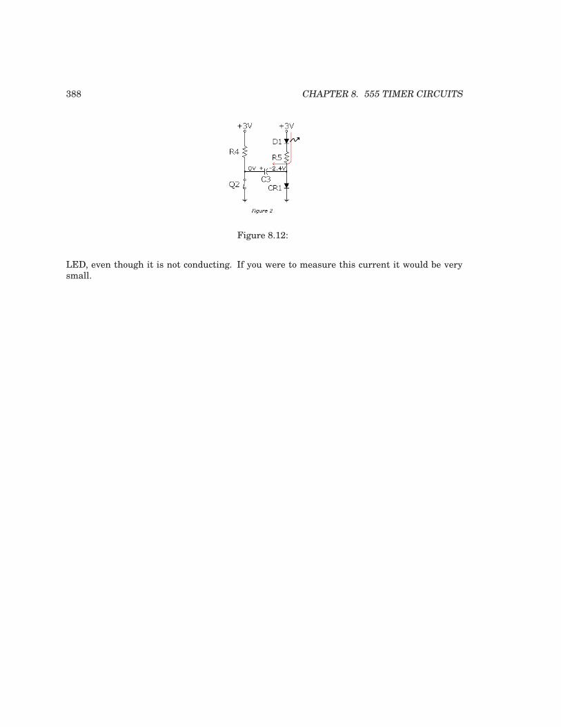
388 CHAPTER 8. 555 TIMER CIRCUITS
Figure 8.12:
LED, even though it is not conducting. If you were to measure this current it would be verysmall.

8.7. CMOS 555 LONG DURATION FLYBACK LED FLASHER 389
8.7 CMOS 555 LONGDURATIONFLYBACKLEDFLASHER
PARTS AND MATERIALS
• Two AAA Batteries
• Battery Clip (Radio Shack catalog # 270-398B)
• U1, U2 - CMOS TLC555 timer IC (Radio Shack catalog # 276-1718 or equivalent)
• Q1 - 2N3906 PNP Transistor (Radio Shack catalog #276-1604 (15 pack) or equivalent)
• Q2 - 2N2222 NPN Transistor (Radio Shack catalog #276-1617 (15 pack) or equivalent)
• D1 - Red light-emitting diode (Radio Shack catalog # 276-041 or equivalent)
• D2 - Blue light-emitting diode (Radio Shack catalog # 276-311 or equivalent)
• R1 - 1.5 MΩ 1/4W 5% Resistor
• R2 - 47 KΩ 1/4W 5% Resistor
• R3,R5 - 10 KΩ 1/4W 5% Resistor
• R4 - 1 MΩ 1/4W 5% Resistor
• R6 - 100 KΩ 1/4W 5% Resistor
• R7 - 1 KΩ 1/4W 5% Resistor
• C1 - 1 F Tantalum Capacitor (Radio Shack catalog # 272-1025 or equivalent)
• C2 - 100 pF Ceramic Disc Capacitor (Radio Shack catalog # 272-123)
• C3 - 100 F Electrolytic Capacitor (Radio Shack catalog 272-1028 or equivalent)
• L1 - 200 H Choke or Inductor (Exact value not critical, see end of chapter)
CROSS-REFERENCES
Lessons In Electric Circuits, Volume 1, chapter 16: Title ”Inductor transient response”Lessons In Electric Circuits, Volume 1, chapter 16: Title ”Why L/R and not LR?”Lessons In Electric Circuits, Volume 3, chapter 4: Title ”The common-emitter amplifier”Lessons In Electric Circuits, Volume 3, chapter 9: Title ”Electrostatic Discharge”Lessons In Electric Circuits, Volume 4, chapter 10: Title ”Monostable multivibrators”
LEARNING OBJECTIVES
• Learn another mode of operation for the 555
• How to handle ESD Parts
• How to use a transistor for a simple gate (resistor transistor inverter)

390 CHAPTER 8. 555 TIMER CIRCUITS
• How inductors can convert power using inductive flyback
• How to make an inductor
SCHEMATIC DIAGRAM
ILLUSTRATION
INSTRUCTIONS
NOTE! This project uses a static sensitive part, the CMOS 555. If you do not use protectionas described in Volume 3, Chapter 9, ElectroStatic Discharge, you run the risk of destroying it.
This particular experiment builds on another experiment, ”Commutating diode” (Volume 6,chapter 5). It is worth reviewing that section before proceeding.
This is the last of the long duration LED flasher series. They have shown how to use aCMOS 555 to flash an LED, and how to boost the voltage of the batteries to allow an LED with

8.7. CMOS 555 LONG DURATION FLYBACK LED FLASHER 391
more voltage drop than the batteries to be used. Here we are doing the same thing, but withan inductor instead of a capacitor.
The basic concept is adapted from another invention, the Joule Thief. A joule thief is asimple transistor oscillator that also uses inductive kickback to light an white light LED froma 11/2 battery, and the LED needs at least 3.6 volts to start conducting! Like the joule thief,it is possible to use 11/2 volts to get this circuit to work. However, since a CMOS 555 is ratedfor 2 volts minimum 11/2 volts is not recommended, but we can take advantage of the extremeefficiency of this circuit. If you want to learn more about the joule thief plenty of informationcan be found on the web.
This circuit can also drive more that 1 or 2 LEDs in series. As the numbers of LEDs goup the ability of the batteries to last a long duration goes down, as the amount of voltage theinductor can generate is somewhat dependent on battery voltage. For the purposes of thisexperiment two dissimilar LEDs were used to demonstrate its independence of LED voltagedrop. The high intensity of the blue LED swamps the red LED, but if you look closely you willfind the red LED is at its maximum brightness. You can use pretty much whatever color ofLEDs you choose for this experiment.
Generally the high voltage created by inductive kickback is something to be eliminated.This circuit uses it, but if you make a mistake with the polarity of the LEDs the blue LED,which is more ESD sensitive, will likely die (this has been verified). An uncontrolled pulsefrom a coil resembles an ESD event. The transistor and the TLC555 can also be at risk.
The inductor in this circuit is probably the least critical part in the design. The term in-ductor is generic, you can also find this component called a choke or a coil. A solenoid coilwould also work, since that is also a type of inductor. So would the coil from a relay. Of allthe components I have used, this is probably the least critical I’ve come across. Indeed, coilsare probably the most practical component you can make yourself that exists. I’ll cover how tomake a coil that will work in this design after the Theory of Operation, but the part shown onthe illustration is a 200H choke I bought from a local electronics retailer.
THEORY OF OPERATION
Both capacitors and inductors store energy. Capacitors try to maintain constant voltage,whereas inductors try to maintain constant current. Both resist change to their respectiveaspect. This is the basis for the flyback transformer, which is a common circuit used in oldCRT circuits and other uses where high voltage is needed with a minimum of fuss. Whenyou charge a coil a magnetic field expands around it, basically it is an electromagnet, and themagnetic field is stored energy. When the current stops this magnetic field collapses, createdelectricity as the field crosses the wires in the coil.
This circuit uses two astable multivibrators. The first multivibrator controls the second.Both are designed for minimum current, as well as the inverter made using Q1. Both theoscillators are very similar, the first has been covered in previous experiments. The problemis it stays on, or is high, 97% of the time. On the previous circuits we used the low state tolight the LED, in this case the high is what turns the second multivibrator on. Using a simpletransistor inverter designed for extra low current solves this problem. This is actually a veryold logic family, RTL, which is short for resistor transistor logic.
The second multivibrator oscillates at 68.6 KHz, with a square wave that is around 50%.This circuit uses the exact same principals as is shown in the Minimum Parts LED Flasher.Again, the largest practical resistors are used to minimize current, and this means a really

392 CHAPTER 8. 555 TIMER CIRCUITS
small capacitor for C2. This high frequency square wave is used to turn Q2 on and off as asimple switch.
Figure 8.13 shows what happens when the Q2 is conducting, and the coil starts to charge.If Q2 were to stay on then an effective short across the batteries would result, but since thisis part of an oscillator this won’t happen. Before the coil can reach it’s maximum current Q2switches, and the switch is open.
Figure 8.13:
Figure 8.14 shows Q2 when it opens, and the coil is charged. The coil tries to maintain thecurrent, but if there is no discharge path it can not do this. If there were no discharge pathis the coil would create a high voltage pulse, seeking to maintain the current that was flowingthrough it, and this voltage would be quite high. However, we have a couple of LEDs in thedischarge path, so the coils pulse quickly goes to the voltage drop of the combined LEDs, thendumps the rest of its charge as current. As a result there is no high voltage generated, butthere is a conversion to the voltage required to light the LEDs.
Figure 8.14:
The LEDs are pulsed, and the light curve follows the discharge curve of the coil fairlyclosely. However, the human eye averages this light output to something we perceive as con-tinuous light.
8.8 HOW TO MAKE AN INDUCTOR
PARTS AND MATERIALS

8.8. HOW TO MAKE AN INDUCTOR 393
• 26 Feet (8 Meters) of 26AWGMagnet Wire (Radio Shack catalog #278-1345 or equivalent)
• 6/32X1.5 inch screw, a M4X30mm screw, or a nail of similar diameter cut down to size,steel or iron, but not stainless
• Matching lock nut (optional)
• Transparent Tape (optional, needed if using screws)
• Super Glue
• Soldering Iron, Solder
As has been mentioned before, this is not a precision part. Inductors in general can havea large variance for many applications, and this one specifically can be off on the high side alarge amount. The target here is greater than 220µH.
If you are using a screw, use one layer of the transparent tape between the threads and thewire. This is to prevent the threads of the screw from cutting into the wire and shorting thecoil out. If you are using a lock nut put it on the screw 1” (25mm) from the head of the screw.Starting around 1” from one end of the wire, use the glue to tack the wire on the head of thenail or screw as shown. Let the glue set.
Figure 8.15:
Wind the wire neatly and tightly 1” the length of screw, again tacking it in place with superglue. (Figure 8.15). You can use a variable speed drill to help with this, as long as you arecareful. Like all power appliances, it can bite you. Hold the wire tight until the glue sets, thenstart winding a second layer over the first. Continue this process until all of the wire exceptthe last 1” is used, using the glue to occasionally tack the wire down. Arrange the wire on thelast layer so the second inductor lead is on the other end of the screw away from the first. Tackthis down for a final time with the glue. Let dry completely.
Gently take a sharp blade and scrap the enamel off each end of the two leads. Tin theexposed copper with the soldering iron and the solder, and you now have a functional inductorthat can be used in this experiment.
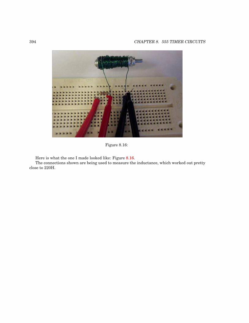
394 CHAPTER 8. 555 TIMER CIRCUITS
Figure 8.16:
Here is what the one I made looked like: Figure 8.16.The connections shown are being used to measure the inductance, which worked out pretty
close to 220H.

8.9. CMOS 555 LONG DURATION RED LED FLASHER 395
8.9 CMOS 555 LONG DURATION RED LED FLASHER
PARTS AND MATERIALS
• Two AAA Batteries
• Battery Clip (Radio Shack catalog # 270-398B)
• A DVM or VOM
• U1 - CMOS TLC555 timer IC (Radio Shack catalog # 276-1718 or equivalent)
• Q1 - 2N3906 PNP Transistor (Radio Shack catalog #276-1604 (15 pack) or equivalent)
• Q2 - 2N2222 NPN Transistor (Radio Shack catalog #276-1617 (15 pack) or equivalent)
• D1 - Red light-emitting diode (Radio Shack catalog # 276-041 or equivalent)
• R1 - 1.5 MΩ 1/4W 5% Resistor
• R2 - 47 KΩ 1/4W 5% Resistor
• R3 - 2.2 KΩ 1/4W 5% Resistor
• R4 - 27 Ω 1/4W 5% Resistor (or test select a better value)
• C1 - 1 F Tantalum Capacitor (Radio Shack catalog 272-1025 or equivalent)
• C2 - 100 F Electrolytic Capacitor (Radio Shack catalog 272-1028 or equivalent)
CROSS-REFERENCES
Lessons In Electric Circuits, Volume 1, chapter 16: “Voltage and current calculations”Lessons In Electric Circuits, Volume 1, chapter 16: “Solving for unknown time”Lessons In Electric Circuits, Volume 3, chapter 4 : “Bipolar Junction Transistors”Lessons In Electric Circuits, Volume 3, chapter 9 : “ElectroStatic Discharge”Lessons In Electric Circuits, Volume 4, chapter 10: “Multivibrators”
LEARNING OBJECTIVES
• Learn a practical application for a RC time constant
• Learn one of several 555 timer Astable Multivibrator Configurations
• Working knowledge of duty cycle
• How to handle ESD sensitive parts
• How to use transistors to improve current gain
• How to calculate the correct resistor for a LED

396 CHAPTER 8. 555 TIMER CIRCUITS
SCHEMATIC DIAGRAM
ILLUSTRATION
INSTRUCTIONS
NOTE! This project uses a static sensitive part, the CMOS 555. If you do not use protectionas described in Volume 3, Chapter 9, ElectroStatic Discharge, you run the risk of destroying it.
The circuit shown in the previous experiment, CMOS 555 Long Duration Minimum Parts
Red LED Flasher, has one big drawback, which is a lack of LED current control. This experi-ment uses the same basic 555 schematic and adds transistorized drivers to correct this.

8.9. CMOS 555 LONG DURATION RED LED FLASHER 397
The parts used for this transistor driver are non critical. It is designed to load the TLC555to an absolute minimum and still turn on Q2 fully. This is important because as the batteryvoltage approaches 2V the drive from the TLC555 is reduced to its minimum values. Bipolartransistors can be good switches.
Since LEDs can have so much variation R4 should be tweaked to match the specific LEDused. The current is limited to 18.5ma with 27Ω and a Vf (LED forward dropping voltage) of2.5V, an LED Vf of 2.1V will draw 33ma, and a LED Vf of 1.5 will draw 56ma. The latter is toomuch current, not to mention what that would do for the battery life. To correct this use 47Ω
if the Vf is 2.1V, and 75Ω if the Vf is 1.5V, assuming the target current is 20ma.You can measure Vf by using the jumper shown in red in the illustration, which will turn
the LED on full time. You can calculate the value of R4 by using the equation:R4 = (3V-Vf) / 0.02AIt was mentioned in the previous experiment that capacitor C2 extended the life of the
batteries. An interesting experiment is to remove this part periodically and see what happens.At first you will notice a dimming of the LED, and after a week or two the circuit will diewithout it, and resume working in a couple of seconds when it is replaced. This flasher willwork for 3 months using fresh alkaline AAA batteries.
THEORY OF OPERATION
The CMOS 555 oscillator was explained fully in the previous experiment, so the transistordriver will be the focus of this explanation.
The transistor driver combines elements of a common collector configuration on Q1, alongwith common emitter configuration on Q2. This allows for very high input resistance whileallowing Q2 to turn on fully. The input resistance of the transistor is the β (gain) of the tran-sistor times the emitter resistor. If Q1 has a gain of 50 (a minimum value) then the driverloads the TLC555 with more than 100KΩ. Transistors can have large variations in gain, evenwithin the same family.
When Q1 turns on 1ma is sent to Q2. This is more than enough to turn Q2 fully, which isreferred to as saturation. Q2 is used as a simple switch for the LED.

398 CHAPTER 8. 555 TIMER CIRCUITS

Appendix A-1
ABOUT THIS BOOK
A-1.1 Purpose
They say that necessity is the mother of invention. At least in the case of this book, that adageis true. As an industrial electronics instructor, I was forced to use a sub-standard textbookduring my first year of teaching. My students were daily frustrated with the many typograph-ical errors and obscure explanations in this book, having spent much time at home strugglingto comprehend the material within. Worse yet were the many incorrect answers in the back ofthe book to selected problems. Adding insult to injury was the $100+ price.
Contacting the publisher proved to be an exercise in futility. Even though the particulartext I was using had been in print and in popular use for a couple of years, they claimed mycomplaint was the first they’d ever heard. My request to review the draft for the next editionof their book was met with disinterest on their part, and I resolved to find an alternative text.
Finding a suitable alternative was more difficult than I had imagined. Sure, there wereplenty of texts in print, but the really good books seemed a bit too heavy on the math and theless intimidating books omitted a lot of information I felt was important. Some of the bestbooks were out of print, and those that were still being printed were quite expensive.
It was out of frustration that I compiled Lessons in Electric Circuits from notes and ideas Ihad been collecting for years. My primary goal was to put readable, high-quality informationinto the hands of my students, but a secondary goal was to make the book as affordable aspossible. Over the years, I had experienced the benefit of receiving free instruction and encour-agement in my pursuit of learning electronics from many people, including several teachersof mine in elementary and high school. Their selfless assistance played a key role in my ownstudies, paving the way for a rewarding career and fascinating hobby. If only I could extendthe gift of their help by giving to other people what they gave to me . . .
So, I decided to make the book freely available. More than that, I decided to make it ”open,”following the same development model used in the making of free software (most notably thevarious UNIX utilities released by the Free Software Foundation, and the Linux operating
399

400 APPENDIX A-1. ABOUT THIS BOOK
system, whose fame is growing even as I write). The goal was to copyright the text – so as toprotect my authorship – but expressly allow anyone to distribute and/or modify the text to suittheir own needs with a minimum of legal encumbrance. This willful and formal revoking ofstandard distribution limitations under copyright is whimsically termed copyleft. Anyone can”copyleft” their creative work simply by appending a notice to that effect on their work, butseveral Licenses already exist, covering the fine legal points in great detail.
The first such License I applied to my work was the GPL – General Public License – of theFree Software Foundation (GNU). The GPL, however, is intended to copyleft works of computersoftware, and although its introductory language is broad enough to cover works of text, itswording is not as clear as it could be for that application. When other, less specific copyleftLicenses began appearing within the free software community, I chose one of them (the DesignScience License, or DSL) as the official notice for my project.
In ”copylefting” this text, I guaranteed that no instructor would be limited by a text insuffi-cient for their needs, as I had been with error-ridden textbooks from major publishers. I’m surethis book in its initial form will not satisfy everyone, but anyone has the freedom to change it,leveraging my efforts to suit variant and individual requirements. For the beginning studentof electronics, learn what you can from this book, editing it as you feel necessary if you comeacross a useful piece of information. Then, if you pass it on to someone else, you will be givingthem something better than what you received. For the instructor or electronics professional,feel free to use this as a reference manual, adding or editing to your heart’s content. Theonly ”catch” is this: if you plan to distribute your modified version of this text, you must givecredit where credit is due (to me, the original author, and anyone else whose modifications arecontained in your version), and you must ensure that whoever you give the text to is aware oftheir freedom to similarly share and edit the text. The next chapter covers this process in moredetail.
It must be mentioned that although I strive to maintain technical accuracy in all of thisbook’s content, the subject matter is broad and harbors many potential dangers. Electricitymaims and kills without provocation, and deserves the utmost respect. I strongly encourageexperimentation on the part of the reader, but only with circuits powered by small batterieswhere there is no risk of electric shock, fire, explosion, etc. High-power electric circuits shouldbe left to the care of trained professionals! The Design Science License clearly states thatneither I nor any contributors to this book bear any liability for what is done with its contents.
A-1.2 The use of SPICE
One of the best ways to learn how things work is to follow the inductive approach: to observespecific instances of things working and derive general conclusions from those observations.In science education, labwork is the traditionally accepted venue for this type of learning, al-though in many cases labs are designed by educators to reinforce principles previously learnedthrough lecture or textbook reading, rather than to allow the student to learn on their ownthrough a truly exploratory process.
Having taught myself most of the electronics that I know, I appreciate the sense of frustra-tion students may have in teaching themselves from books. Although electronic componentsare typically inexpensive, not everyone has the means or opportunity to set up a laboratoryin their own homes, and when things go wrong there’s no one to ask for help. Most textbooks

A-1.3. ACKNOWLEDGEMENTS 401
seem to approach the task of education from a deductive perspective: tell the student howthings are supposed to work, then apply those principles to specific instances that the studentmay or may not be able to explore by themselves. The inductive approach, as useful as it is, ishard to find in the pages of a book.
However, textbooks don’t have to be this way. I discovered this when I started to learn acomputer program called SPICE. It is a text-based piece of software intended to model circuitsand provide analyses of voltage, current, frequency, etc. Although nothing is quite as good asbuilding real circuits to gain knowledge in electronics, computer simulation is an excellent al-ternative. In learning how to use this powerful tool, I made a discovery: SPICE could be usedwithin a textbook to present circuit simulations to allow students to ”observe” the phenomenafor themselves. This way, the readers could learn the concepts inductively (by interpretingSPICE’s output) as well as deductively (by interpreting my explanations). Furthermore, inseeing SPICE used over and over again, they should be able to understand how to use it them-selves, providing a perfectly safe means of experimentation on their own computers with circuitsimulations of their own design.
Another advantage to including computer analyses in a textbook is the empirical verifi-cation it adds to the concepts presented. Without demonstrations, the reader is left to takethe author’s statements on faith, trusting that what has been written is indeed accurate. Theproblem with faith, of course, is that it is only as good as the authority in which it is placed andthe accuracy of interpretation through which it is understood. Authors, like all human beings,are liable to err and/or communicate poorly. With demonstrations, however, the reader canimmediately see for themselves that what the author describes is indeed true. Demonstrationsalso serve to clarify the meaning of the text with concrete examples.
SPICE is introduced early in volume I (DC) of this book series, and hopefully in a gentleenough way that it doesn’t create confusion. For those wishing to learn more, a chapter in thisvolume (volume V) contains an overview of SPICE with many example circuits. There maybe more flashy (graphic) circuit simulation programs in existence, but SPICE is free, a virtuecomplementing the charitable philosophy of this book very nicely.
A-1.3 Acknowledgements
First, I wish to thank my wife, whose patience during those many and long evenings (andweekends!) of typing has been extraordinary.
I also wish to thank those whose open-source software development efforts have made thisendeavor all the more affordable and pleasurable. The following is a list of various free com-puter software used to make this book, and the respective programmers:
• GNU/Linux Operating System – Linus Torvalds, Richard Stallman, and a host of otherstoo numerous to mention.
• Vim text editor – Bram Moolenaar and others.
• Xcircuit drafting program – Tim Edwards.
• SPICE circuit simulation program – too many contributors to mention.
• TEX text processing system – Donald Knuth and others.

402 APPENDIX A-1. ABOUT THIS BOOK
• Texinfo document formatting system – Free Software Foundation.
• LATEX document formatting system – Leslie Lamport and others.
• Gimp image manipulation program – too many contributors to mention.
• Winscope signal analysis software – Dr. Constantin Zeldovich. (Free for personal andacademic use.)
Appreciation is also extended to Robert L. Boylestad, whose first edition of IntroductoryCircuit Analysis taught me more about electric circuits than any other book. Other importanttexts in my electronics studies include the 1939 edition of The ”Radio” Handbook, BernardGrob’s second edition of Introduction to Electronics I, and Forrest Mims’ original Engineer’sNotebook.
Thanks to the staff of the Bellingham Antique Radio Museum, who were generous enoughto let me terrorize their establishment with my camera and flash unit.
I wish to specifically thank Jeffrey Elkner and all those at Yorktown High School for beingwilling to host my book as part of their Open Book Project, and to make the first effort in con-tributing to its form and content. Thanks also to David Sweet (website: (http://www.andamooka.org) )and Ben Crowell (website: (http://www.lightandmatter.com) ) for providing encourage-ment, constructive criticism, and a wider audience for the online version of this book.
Thanks to Michael Stutz for drafting his Design Science License, and to Richard Stallmanfor pioneering the concept of copyleft.
Last but certainly not least, many thanks to my parents and those teachers of mine whosaw in me a desire to learn about electricity, and who kindled that flame into a passion fordiscovery and intellectual adventure. I honor you by helping others as you have helped me.
Tony Kuphaldt, July 2001
”A candle loses nothing of its light when lighting another”
Kahlil Gibran

Appendix A-2
CONTRIBUTOR LIST
A-2.1 How to contribute to this book
As a copylefted work, this book is open to revision and expansion by any interested parties.The only ”catch” is that credit must be given where credit is due. This is a copyrighted work:it is not in the public domain!
If you wish to cite portions of this book in a work of your own, you must follow the sameguidelines as for any other copyrighted work. Here is a sample from the Design Science Li-cense:
The Work is copyright the Author. All rights to the Work are re servedby the Author, except as specifically described below. This Licensedescribes the terms and conditions under which the Author pe rmits youto copy, distribute and modify copies of the Work.
In addition, you may refer to the Work, talk about it, and (asdictated by "fair use") quote from it, just as you would anycopyrighted material under copyright law.
Your right to operate, perform, read or otherwise interpret and/orexecute the Work is unrestricted; however, you do so at your o wn risk,because the Work comes WITHOUT ANY WARRANTY -- see Section 7 ( "NOWARRANTY") below.
If you wish to modify this book in any way, you must document the nature of those modifi-cations in the ”Credits” section along with your name, and ideally, information concerning howyou may be contacted. Again, the Design Science License:
Permission is granted to modify or sample from a copy of the Wo rk,
403

404 APPENDIX A-2. CONTRIBUTOR LIST
producing a derivative work, and to distribute the derivati ve workunder the terms described in the section for distribution ab ove,provided that the following terms are met:
(a) The new, derivative work is published under the terms of t hisLicense.
(b) The derivative work is given a new name, so that its name ortitle can not be confused with the Work, or with a version ofthe Work, in any way.
(c) Appropriate authorship credit is given: for the differe ncesbetween the Work and the new derivative work, authorship isattributed to you, while the material sampled or used fromthe Work remains attributed to the original Author; appropr iatenotice must be included with the new work indicating the natu reand the dates of any modifications of the Work made by you.
Given the complexities and security issues surrounding the maintenance of files comprisingthis book, it is recommended that you submit any revisions or expansions to the original author(Tony R. Kuphaldt). You are, of course, welcome to modify this book directly by editing yourown personal copy, but we would all stand to benefit from your contributions if your ideas wereincorporated into the online “master copy” where all the world can see it.
A-2.2 Credits
All entries arranged in alphabetical order of surname. Major contributions are listed by indi-vidual name with some detail on the nature of the contribution(s), date, contact info, etc. Minorcontributions (typo corrections, etc.) are listed by name only for reasons of brevity. Please un-derstand that when I classify a contribution as “minor,” it is in no way inferior to the effortor value of a “major” contribution, just smaller in the sense of less text changed. Any and allcontributions are gratefully accepted. I am indebted to all those who have given freely of theirown knowledge, time, and resources to make this a better book!
A-2.2.1 Dennis Crunkilton
• Date(s) of contribution(s): January 2006 to present
• Nature of contribution: Mini table of contents, all chapters except appedicies; html,latex, ps, pdf; See Devel/tutorial.html; 01/2006.
• Nature of contribution: CH 4, section: Induction motor, 09/2007.
• Nature of contribution: CH 4, section: Induction motor, large 02/2010.
• Contact at: dcrunkilton(at)att(dot)net
A-2.2. CREDITS 405
A-2.2.2 Tony R. Kuphaldt
• Date(s) of contribution(s): 1996 to present
• Nature of contribution: Original author.
• Contact at: [email protected]
A-2.2.3 Bill Marsden
• Date(s) of contribution(s): August 2008
• Nature of contribution: Original author: “555 Schmidt trigger” Section, Chapter 7.
• Contact at: bill marsden2(at)hotmail(dot)com
A-2.2.4 Forrest M. Mims III
• Date(s) of contribution(s):February 2008
• Nature of contribution:Ch 5; Clarification concerning LEDs as photosensors.
• Contact at: FMims(at)aol.com
A-2.2.5 Your name here
• Date(s) of contribution(s): Month and year of contribution
• Nature of contribution: Insert text here, describing how you contributed to the book.
• Contact at: my [email protected]
A-2.2.6 Typo corrections and other “minor” contributions
• line-allaboutcircuits.com (June 2005) Typographical error correction in Volumes 1,2,3,5,various chapters ,(:s/visa-versa/vice versa/).
• The students of Bellingham Technical College’s Instrumentation program.
• Colin Creitz (May 2007) Chapters: several, s/it’s/its.
• Jeff DeFreitas (March 2006)Improve appearance: replace “/” and ”/” Chapters: A1, A2.
• Don Stalkowski (June 2002) Technical help with PostScript-to-PDF file format conver-sion.
• Joseph Teichman (June 2002) Suggestion and technical help regarding use of PNGimages instead of JPEG.
• Michael Warner (April 2002) Suggestions for a section describing home laboratory setup.

406 APPENDIX A-2. CONTRIBUTOR LIST
• [email protected] (August 2007) Ch 1, s/starting/started .
• [email protected] (August 2007) Ch 6, s/and and off/on and off/ .
• Timothy [email protected] (Feb 2008) Changed default roman fontto newcent.
• Imranullah Syed (Feb 2008) Suggested centering of uncaptioned schematics.
• [email protected], [email protected] (May 2008) Changedimage 05320.png to agree with image 05321.png¡/item
• [email protected] (April 2009) Ch4, s/Try changed/Try changing/¡/item
• [email protected] (August 2009) added <section> tags to ”555 Schmitt trig-ger”, d ic.sml .
• [email protected] (August 2009) correction to image 05198.eps &.png.
• [email protected] (January 2010) added <proofread> tag to ”555Schmitt trigger”.
• [email protected] (January 2010) Ch2, s/The less ressistance/ Themoreresistance.
• Bill [email protected] (April 2010) added new CROSS-REFERENCE to”555 Schmitt trigger”.
• [email protected] (September 2010) Ch6, s/useable/usable/ .
• D. Crunkilton (June 2011) hi.latex, header file; updated link to openbookproject.net .
• hillshaveeyes57 (January 2013) Ch8, Hysteretic Oscillator, Swap R3 and R4 with de-scription in parts list.
• Bill [email protected] (January 2014) Ch8, s/circuits operation/circuit’soperation.

Appendix A-3
DESIGN SCIENCE LICENSE
Copyright c© 1999-2000 Michael Stutz [email protected] copying of this document is permitted, in any medium.
A-3.1 0. Preamble
Copyright law gives certain exclusive rights to the author of a work, including the rightsto copy, modify and distribute the work (the ”reproductive,” ”adaptative,” and ”distribution”rights).
The idea of ”copyleft” is to willfully revoke the exclusivity of those rights under certainterms and conditions, so that anyone can copy and distribute the work or properly attributedderivative works, while all copies remain under the same terms and conditions as the original.
The intent of this license is to be a general ”copyleft” that can be applied to any kind of workthat has protection under copyright. This license states those certain conditions under whicha work published under its terms may be copied, distributed, and modified.
Whereas ”design science” is a strategy for the development of artifacts as a way to reformthe environment (not people) and subsequently improve the universal standard of living, thisDesign Science License was written and deployed as a strategy for promoting the progress ofscience and art through reform of the environment.
A-3.2 1. Definitions
”License” shall mean this Design Science License. The License applies to any work whichcontains a notice placed by the work’s copyright holder stating that it is published under theterms of this Design Science License.
”Work” shall mean such an aforementioned work. The License also applies to the output ofthe Work, only if said output constitutes a ”derivative work” of the licensed Work as defined bycopyright law.
407

408 APPENDIX A-3. DESIGN SCIENCE LICENSE
”Object Form” shall mean an executable or performable form of the Work, being an embod-iment of the Work in some tangible medium.
”Source Data” shall mean the origin of the Object Form, being the entire, machine-readable,preferred form of the Work for copying and for human modification (usually the language,encoding or format in which composed or recorded by the Author); plus any accompanyingfiles, scripts or other data necessary for installation, configuration or compilation of the Work.
(Examples of ”Source Data” include, but are not limited to, the following: if the Work is animage file composed and edited in ’PNG’ format, then the original PNG source file is the SourceData; if the Work is an MPEG 1.0 layer 3 digital audio recording made from a ’WAV’ formataudio file recording of an analog source, then the original WAV file is the Source Data; if theWork was composed as an unformatted plaintext file, then that file is the the Source Data; ifthe Work was composed in LaTeX, the LaTeX file(s) and any image files and/or custom macrosnecessary for compilation constitute the Source Data.)
”Author” shall mean the copyright holder(s) of the Work.
The individual licensees are referred to as ”you.”
A-3.3 2. Rights and copyright
The Work is copyright the Author. All rights to the Work are reserved by the Author, except asspecifically described below. This License describes the terms and conditions under which theAuthor permits you to copy, distribute and modify copies of the Work.
In addition, you may refer to the Work, talk about it, and (as dictated by ”fair use”) quotefrom it, just as you would any copyrighted material under copyright law.
Your right to operate, perform, read or otherwise interpret and/or execute the Work is un-restricted; however, you do so at your own risk, because the Work comes WITHOUT ANYWARRANTY – see Section 7 (”NO WARRANTY”) below.
A-3.4 3. Copying and distribution
Permission is granted to distribute, publish or otherwise present verbatim copies of the entireSource Data of the Work, in any medium, provided that full copyright notice and disclaimer ofwarranty, where applicable, is conspicuously published on all copies, and a copy of this Licenseis distributed along with the Work.
Permission is granted to distribute, publish or otherwise present copies of the Object Formof the Work, in any medium, under the terms for distribution of Source Data above and alsoprovided that one of the following additional conditions are met:
(a) The Source Data is included in the same distribution, distributed under the terms ofthis License; or
(b) A written offer is included with the distribution, valid for at least three years or foras long as the distribution is in print (whichever is longer), with a publicly-accessible address(such as a URL on the Internet) where, for a charge not greater than transportation and mediacosts, anyone may receive a copy of the Source Data of the Work distributed according to thesection above; or

A-3.5. 4. MODIFICATION 409
(c) A third party’s written offer for obtaining the Source Data at no cost, as described inparagraph (b) above, is included with the distribution. This option is valid only if you are anon-commercial party, and only if you received the Object Form of the Work along with suchan offer.
You may copy and distribute the Work either gratis or for a fee, and if desired, you mayoffer warranty protection for the Work.
The aggregation of the Work with other works which are not based on the Work – such asbut not limited to inclusion in a publication, broadcast, compilation, or other media – does notbring the other works in the scope of the License; nor does such aggregation void the terms ofthe License for the Work.
A-3.5 4. Modification
Permission is granted to modify or sample from a copy of the Work, producing a derivativework, and to distribute the derivative work under the terms described in the section for distri-bution above, provided that the following terms are met:
(a) The new, derivative work is published under the terms of this License.
(b) The derivative work is given a new name, so that its name or title can not be confusedwith the Work, or with a version of the Work, in any way.
(c) Appropriate authorship credit is given: for the differences between the Work and thenew derivative work, authorship is attributed to you, while the material sampled or used fromthe Work remains attributed to the original Author; appropriate notice must be included withthe new work indicating the nature and the dates of any modifications of the Work made byyou.
A-3.6 5. No restrictions
You may not impose any further restrictions on the Work or any of its derivative works beyondthose restrictions described in this License.
A-3.7 6. Acceptance
Copying, distributing or modifying the Work (including but not limited to sampling from theWork in a new work) indicates acceptance of these terms. If you do not follow the terms of thisLicense, any rights granted to you by the License are null and void. The copying, distribution ormodification of the Work outside of the terms described in this License is expressly prohibitedby law.
If for any reason, conditions are imposed on you that forbid you to fulfill the conditions ofthis License, you may not copy, distribute or modify the Work at all.
If any part of this License is found to be in conflict with the law, that part shall be inter-preted in its broadest meaning consistent with the law, and no other parts of the License shallbe affected.

410 APPENDIX A-3. DESIGN SCIENCE LICENSE
A-3.8 7. No warranty
THE WORK IS PROVIDED ”AS IS,” AND COMES WITH ABSOLUTELY NO WARRANTY,EXPRESS OR IMPLIED, TO THE EXTENT PERMITTED BY APPLICABLE LAW, INCLUD-ING BUT NOT LIMITED TO THE IMPLIED WARRANTIES OF MERCHANTABILITY ORFITNESS FOR A PARTICULAR PURPOSE.
A-3.9 8. Disclaimer of liability
IN NO EVENT SHALL THE AUTHOR OR CONTRIBUTORS BE LIABLE FOR ANY DI-RECT, INDIRECT, INCIDENTAL, SPECIAL, EXEMPLARY, OR CONSEQUENTIAL DAM-AGES (INCLUDING, BUT NOT LIMITED TO, PROCUREMENT OF SUBSTITUTE GOODSOR SERVICES; LOSS OF USE, DATA, OR PROFITS; OR BUSINESS INTERRUPTION)HOWEVER CAUSED AND ON ANY THEORY OF LIABILITY, WHETHER IN CONTRACT,STRICT LIABILITY, OR TORT (INCLUDINGNEGLIGENCEOROTHERWISE) ARISING INANY WAY OUT OF THE USE OF THIS WORK, EVEN IF ADVISED OF THE POSSIBILITYOF SUCH DAMAGE.
END OF TERMS AND CONDITIONS
[$Id: dsl.txt,v 1.25 2000/03/14 13:14:14 m Exp m $]

Index
β ratio, 257555 timer, 312, 315, 318555 timer IC, 365
AC, 145AC coupling, oscilloscope, 196, 210Active-high input, 363Active-low input, 363Alligator clip, 19Alternating current, 145Alternator, 164Amp, 36Ampere, 36Amplifier circuit, 134Amplifier impedance, 244Amplifier, inverting, 247, 299Amplifier, noninverting, 299Amplifier, operational, 252Amplitude, 185Analog, 289, 331Analog computer, 133, 144Analog multimeter, 16Antiresonance, 192Astable multivibrator, 275, 312Audio taper potentiometer, 87, 117, 155Autoranging meter, 18
Banana plugs and jacks, 99Battery, 19Beta ratio, 257Bias current, op-amp, 309Binding posts, 99Bounce, switch contact, 345, 353Breadboard, 22
Calculus, 143, 306Calibration drift—hyperpage, 107
Capacitor, decoupling, 199Choke, 191Choke, filter, 225Circuit, 29Circuit, short, 32Common-mode voltage, 267Commonality, electrical, 24Computer simulation, 76Computer, analog, 133, 144Constant-current diode, 263Contact bounce, 345, 353Continuity, 22Continuity vs. commonality, 24Current divider, 84Current mirror, 263, 315Current regulator, 257Current, definition, 36
DC, 59Debouncing, switch, 354Decoupling capacitor, 199Derivative, calculus, 143, 306Detector, null, 124Differential amplifier, 267, 270Differential pair, 267, 270Differentiation, calculus, 143, 306Digital, 289, 331Digital multimeter, 16Diode, 26Diode equation, 258Diode, constant-current, 263Direct current, 59Discontinuity, 29Divider, current, 84Divider, voltage, 70Drift, calibration, 107Duty cycle, 312
411

412 INDEX
E, symbol for voltage, 44Effect, Seebeck, 110Electrical continuity, 22Electrical shock hazard, 26Electrically common points, 24, 64Electromagnetic induction, 57Electromagnetism, 56Equation, diode, 258Experiment: 3-bit binary counter, 359Experiment: 4-wire resistance measurement,
127Experiment: 555 audio oscillator, 311Experiment: 555 ramp generator, 314Experiment: 555 Schmitt Trigger, 366Experiment: 7-segment display, 361Experiment: AC power supply, 147Experiment: Alternator, 164Experiment: Ammeter usage, 35Experiment: Audio detector, 155Experiment: Audio oscillator, 274Experiment: Basic gate function, 333Experiment: BJT switch, 230Experiment: Bridge rectifier, 218Experiment: Capacitor charging and discharg-
ing, 138Experiment: Center-tap rectifier, 213Experiment: Class B audio amplifier, 321Experiment: Common-emitter amplifier, 246Experiment: Commutating diode, 203Experiment: Current divider, 78Experiment: Current mirror, 255Experiment: Differential amplifier, 266Experiment: Electromagnetic field sensor, AC,
160Experiment: Electromagnetic induction, 57Experiment: Electromagnetism, 55Experiment: Electrostatic field sensor, AC, 162Experiment: Half-wave rectifier, 205Experiment: High-impedance voltmeter, 301Experiment: Induction motor, 170, 174Experiment: Integrator, 305Experiment: JFET current regulator, 261Experiment: Keyboard as signal generator, 183Experiment: LED sequencer, 347Experiment: Multi-stage amplifier, 251Experiment: Multimeter, 112
Experiment: NAND gate S-R enabled latch,341
Experiment: NAND gate S-R flip-flop, 343Experiment: Noninverting amplifier, 298Experiment: Nonlinear resistance, 45Experiment: NOR gate S-R latch, 337Experiment: Ohm’s Law, 42Experiment: Ohmmeter usage, 21Experiment: Oscilloscope, PC, 186Experiment: Parallel batteries, 63Experiment: Phase shift, 177Experiment: Potato battery, 136Experiment: Potentiometer as rheostat, 93Experiment: Potentiometer as voltage divider,
87Experiment: Potentiometric voltmeter, 122Experiment: Power dissipation, 48Experiment: Precision potentiometer, 99Experiment: Precision voltage follower, 294Experiment: Pulsed-light sensor, 238Experiment: PWM power controller, 317Experiment: Rate-of-change indicator, 142Experiment: Rectifier/filter, 221Experiment: Rheostat range limiting, 102Experiment: Series batteries, 60Experiment: Signal coupling, 194Experiment: Simple circuit, 28Experiment: Simple combination lock, 356Experiment: Simple op-amp, 269Experiment: Sound cancellation, 180Experiment: Static electricity sensor, 235Experiment: Switch in circuit, 53Experiment: Tank circuit, 191Experiment: Thermoelectricity, 109Experiment: Transformer, homemade, 151Experiment: Vacuum tube audio amplifier, 277Experiment: Variable inductor, 153Experiment: Voltage averager, 131Experiment: Voltage comparator, 291Experiment: Voltage detector, sensitive, 117Experiment: Voltage divider, 67Experiment: Voltage follower, 241Experiment: Voltage regulator, 227Experiment: Voltmeter usage, 15Experiment: Waveform analysis, 189

INDEX 413
Feedback, 290, 295Feedback, negative, 248Field winding, alternator, 164Filter, 223Filter choke, 225Floating input, defined, 335, 353Frequency, 185Frequency domain, 190Full-wave rectification, 214Function generator, 184Fundamental frequency, 190Fuse, 37Fuse, slow-blow, 147
Generator, 19, 164Generator, AC signal, 184
Half-wave rectification, 206Harmonics, 185Hazard, electrical shock, 26Headphone, 117Heat sink, 223Hysteresis, 338
I, symbol for current, 44IC, 202, 289, 331Illegal state, 338Impedance matching, 120, 158Impedance, amplifier, 244Impedance, definition, 120, 158Induction, electromagnetic, 57Inductive kickback—hyperpage, 56, 120, 158Integrated circuit, 202, 289, 331Integration, calculus, 306Interactive adjustment, 101Invalid state, 338Inverting amplifier, 247, 299
Joule’s Law, 51Jumper wire, 19
KCL, 84Kirchhoff ’s Current Law, 84Kirchhoff ’s Voltage Law, 70KVL, 70
Latch-up, 304
Latched state, 338LED, 18Light-Emitting Diode, 18Linear taper potentiometer, 87, 117, 155
Magnet wire, 55, 151Maximum Power Transfer Theorem, 120, 158Megger, 128Meter movement, 112Meter overrange, 18Metric prefix, 25, 38Monostable multivibrator, 354Motor, induction, 168Motor, synchronous, 168Movement, meter, 112Multimeter, 16Multivibrator, 275, 312Multivibrator, monostable, 354
Negative feedback, 248Noninverting amplifier, 299Null detector, 124Null-balance voltmeter, 124
Ohm, 22Ohm’s Law, 44Ohm’s Law, AC version, 178Op-amp, 267, 270Operational amplifier, 252, 267, 270, 290Operational amplifier, programmable, 273Oscilloscope, 187Oscilloscope coupling, 196, 210Overrange, meter, 18
Pair, differential, 267, 270Parallel, 64, 105Permeability, 154Phase shift, 178Photocell, 27Polarity, 19, 31Potentiometer, 87Potentiometer as rheostat, 94Potentiometer, linear vs. audio taper, 87Potentiometric voltmeter, 124Power supply, 145Power, definition, 51

414 INDEX
Programmable op-amp, 273Pulldown resistor, 352Pulse-width modulation, 319PWM power control, 319
Q, inductor quality factor—hyperpage, 192
R, symbol for resistance, 44Race condition, 339Rail voltage, 296Rectification, full-wave, 214Rectification, half-wave, 206Rectifying diode, 26Regulator, current, 257Reluctance, magnetic, 152Reset state, 338Resistance, definition, 22Resistor color code, 24Resistor, pulldown, 352Resistor, shunt, 243Resonance, 192Resonant frequency, 192Rheostat, 94Ring-lug terminal, 165Ripple voltage, 208, 223
Schmitt trigger, 366Seebeck effect, 110Semiconductor, 202Series, 61, 104Series-parallel, 66Set state, 338Shielding, 161, 163Shock hazard, 26Short circuit, 32Shunt resistor, 243Signal generator, 184Simulation, computer, 76Slip ring, alternator, 165Soldering, 148Span calibration, 105SPICE, 76Split phase, 219Stator winding, alternator, 164Strip, terminal, 34Switch, 53
Switch debouncing, 354
Tank circuit, 192Terminal strip, 34Terminal, ring lug, 165Thermal runaway, 259, 263Thermocouple, 110Time constant, 140Time domain, 190Transformer, 117, 145Transistor, 96Transistor, junction field-effect, 236
Unit, ampere, 36Unit, ohm, 22Unit, volt, 18Unit, watt, 51
Volt, 18Voltage divider, 70Voltage follower, 242, 270, 295Voltage, common-mode, 267Voltage, definition, 18Voltage, polarity, 19, 31Voltage, ripple, 208, 223
Watt, 51Wire, magnet, 55
Z, symbol for impedance, 120, 158Zero calibration, 105

INDEX 415
.


![2016年宁波市房地产市场研究报告 [周报] · 2016年第44周(2016.10.24-10.30) 6/14 2016·宁波市房地产市场周报 地址/Add:宁波市江东区和丰创意广场意庭楼6F](https://static.fdocuments.net/doc/165x107/5b5af8717f8b9a885b8d1a1b/2016-20164420161024-1030.jpg)