2007_04: Examples of broadband extraction of - Simberian
21
Examples of broadband extraction of transmission line parameters with Simbeor www.simberian.com Simbeor: Easy-to-Use, Efficient and Cost-Effective… Simbeor Application Note #2007_04, September 2007 © 2007 Simberian Inc.
Transcript of 2007_04: Examples of broadband extraction of - Simberian

Examples of broadband extraction of transmission line parameters with
Simbeor
www.simberian.com
Simbeor: Easy-to-Use, Efficient and Cost-Effective…
Simbeor Application Note #2007_04, September 2007 © 2007 Simberian Inc.

10/7/2008 © 2007 Simberian Inc. 2
IntroductionGoal is to illustrate how Simbeor 2007 can be used to build 3D full-wave broad-band transmission line models for different planar circuit manufacturing technologies

10/7/2008 © 2007 Simberian Inc. 3
Simbeor technology at a glancePerforms 3D full-wave analysis of transmission line segment and automatically extract frequency-dependent modal and RLGC matrix parameters per unit length for W-element models of multiconductor linesUses broadband and causal dielectric modelsSimulates transition to skin-effect, shape and proximity effects at medium frequenciesAccounts for skin-effect, dispersion and edge effect at high frequenciesHas conductor models valid and causal over 5-6 frequency decades in generalAccounts for conductor surface roughness and finish

10/7/2008 © 2007 Simberian Inc. 4
PCB micro-strip line exampleExample TLines\ Comparisons\ PCB\ PCB.esx8 mil wide 1.6 mil thick strip on dielectric substrate with Dk=4.0 and LT=0.04 at 1 GHz. Substrate thickness 4 mil, plane thickness 2 mil.

10/7/2008 © 2007 Simberian Inc. 5
PCB micro-strip example: Attenuation8 mil wide 1.6 mil thick strip on dielectric substrate with Dk=4.0 and LT=0.04 at 1 GHz modeled as wideband Debye. Substrate thickness 4 mil, plane thickness 2 mil.
Simbeor results: red curve is complete losses with surface roughness 2 um
Skin-effect transition is around 3 MHz
Dielectric Loss Only
Metal Loss Only
Total Loss with2 um roughness
Typical Erroneous Saturation
Transition frq is too
high
Accurate transition to skin-effect
From “Accounting for High Frequency Transmission Line Loss Effects in HFSS”, Andrew Byers, Tektronix, 2003 HFSS Users Workshop, http://www.ansoft.com/workshops/hfworkshop03 Andy_Byers_Tektronix.pdf

10/7/2008 © 2007 Simberian Inc. 6
PCB differential micro-strip line example7.5 mil wide 2.2 mil thick strips 20 mil apart. Dielectric substrate with Dk=4.1 and LT=0.02 at 1 GHz. Substrate thickness 4.5 mil, plane thickness 0.594 mil.
Example PCB_MCM\16LBoardModels\16LBoardModels.esx

10/7/2008 © 2007 Simberian Inc. 7
Modal parameters of the differential micro-strip line with metal surface roughness 0.5 um
Magnitude of characteristic impedance and attenuation of the differential and common modes
Phase and group delays p.u.l. of the differential and common modes – illustrates skin and dielectric dispersion effects
Effect of Dispersion
Skin Effects in thin plane
Differential mode impedance
Common mode impedance
Attenuations

10/7/2008 © 2007 Simberian Inc. 8
RLGC parameters of the differential micro-strip line with metal surface roughness 0.5 um
Elements of p.u.l. resistance and inductance matrices
Elements of p.u.l. conductance and capacitance matrices
Skin-effect in 12 um plane
10/7/2008 © 2007 Simberian Inc. 9
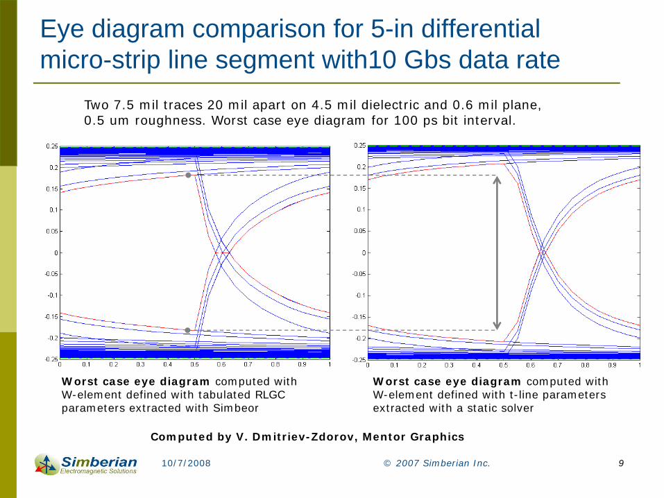
Eye diagram comparison for 5-in differential micro-strip line segment with10 Gbs data rate
Two 7.5 mil traces 20 mil apart on 4.5 mil dielectric and 0.6 mil plane, 0.5 um roughness. Worst case eye diagram for 100 ps bit interval.
Worst case eye diagram computed with W-element defined with t-line parameters extracted with a static solver
Worst case eye diagram computed with W-element defined with tabulated RLGC parameters extracted with Simbeor
Computed by V. Dmitriev-Zdorov, Mentor Graphics

10/7/2008 © 2007 Simberian Inc. 10
Eye diagram comparison for 5-in differential micro-strip line segment with 20 Gbs data rate
Two 7.5 mil traces 20 mil apart on 4.5 mil dielectric and 0.6 mil plane, 0.5 um roughness. Worst case eye diagram for 50 ps bit interval – May affect channel budget!
Worst case eye diagram computed with W-element defined with tabulated RLGC parameters extracted with Simbeor
Worst case eye diagram computed with W-element defined with t-line parameters extracted with a static solver
Computed by V. Dmitriev-Zdorov, Mentor Graphics
10/7/2008 © 2007 Simberian Inc. 11
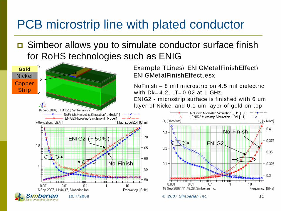
PCB microstrip line with plated conductorSimbeor allows you to simulate conductor surface finish for RoHS technologies such as ENIG
NoFinish – 8 mil microstrip on 4.5 mil dielectric with Dk=4.2, LT=0.02 at 1 GHz. ENIG2 - microstrip surface is finished with 6 um layer of Nickel and 0.1 um layer of gold on top
No Finish
ENIG2 (+50%)No Finish
ENIG2
GoldNickelCopperStrip
Example TLines\ ENIGMetalFinishEffect\ENIGMetalFinishEffect.esx
10/7/2008 © 2007 Simberian Inc. 12
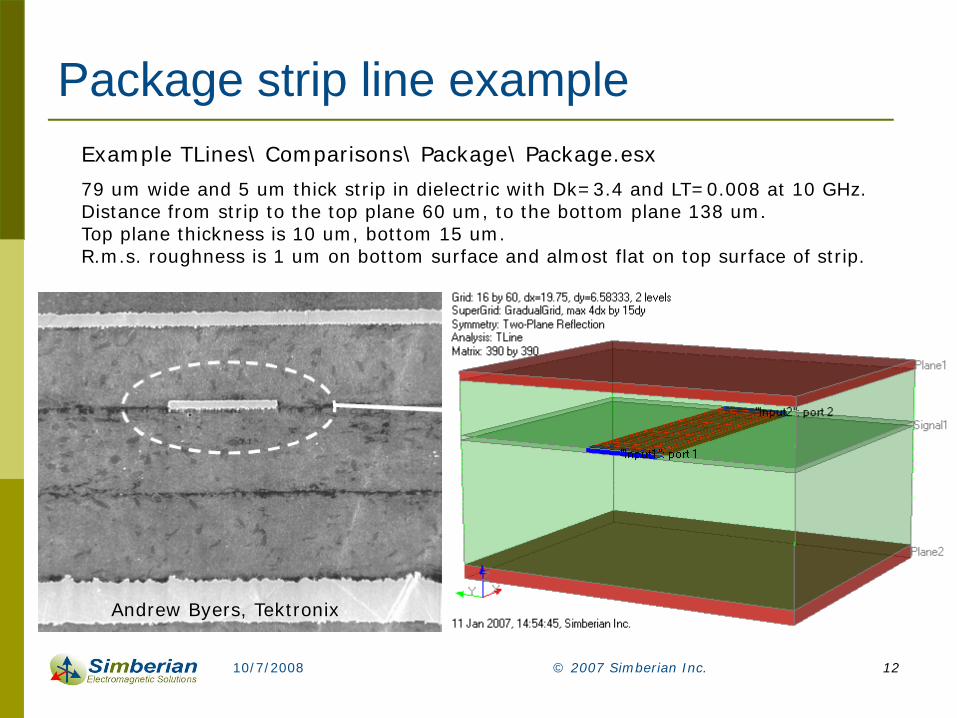
Package strip line exampleExample TLines\ Comparisons\ Package\ Package.esx79 um wide and 5 um thick strip in dielectric with Dk=3.4 and LT=0.008 at 10 GHz. Distance from strip to the top plane 60 um, to the bottom plane 138 um. Top plane thickness is 10 um, bottom 15 um. R.m.s. roughness is 1 um on bottom surface and almost flat on top surface of strip.
Andrew Byers, Tektronix
10/7/2008 © 2007 Simberian Inc. 13
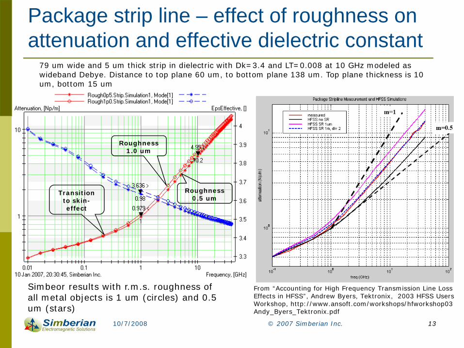
Package strip line – effect of roughness on attenuation and effective dielectric constant
Simbeor results with r.m.s. roughness of all metal objects is 1 um (circles) and 0.5 um (stars)
79 um wide and 5 um thick strip in dielectric with Dk=3.4 and LT=0.008 at 10 GHz modeled as wideband Debye. Distance to top plane 60 um, to bottom plane 138 um. Top plane thickness is 10 um, bottom 15 um
Roughness0.5 um
Roughness 1.0 um
Transition to skin-effect
From “Accounting for High Frequency Transmission Line Loss Effects in HFSS”, Andrew Byers, Tektronix, 2003 HFSS Users Workshop, http://www.ansoft.com/workshops/hfworkshop03 Andy_Byers_Tektronix.pdf

10/7/2008 © 2007 Simberian Inc. 14
Package strip line – effect of dielectric and metal losses on attenuation and dispersion
79 um wide and 5 um thick strip in dielectric with Dk=3.4 and LT=0.008 at 10 GHz modeled as wideband Debye. Distance to top plane 60 um, to bottom plane 138 um. Top plane thickness is 10 um, bottom 15 um
Dielectric Loss Only
Metal Loss Only (1 um)
Total Loss with 1 um roughness

10/7/2008 © 2007 Simberian Inc. 15
Package strip line with different roughness for top and bottom surfaces of strip
Broadband analysis: transition to skin-effect, skin-effect with roughness, proximity and edge-effects…
Rough
FlatTransition to skin-effect Rough
FlatLossless
Lossy
79 um wide and 5 um thick strip in dielectric with Dk=3.4 and LT=0.008 at 10 GHz modeled as wideband Debye. Distance to top plane 60 um, to bottom plane 138 um. Top plane thickness is 10 um, bottom 15 um. RMS roughness is 1 um on all surfaces except top of the strip, that is flat.

10/7/2008 © 2007 Simberian Inc. 16
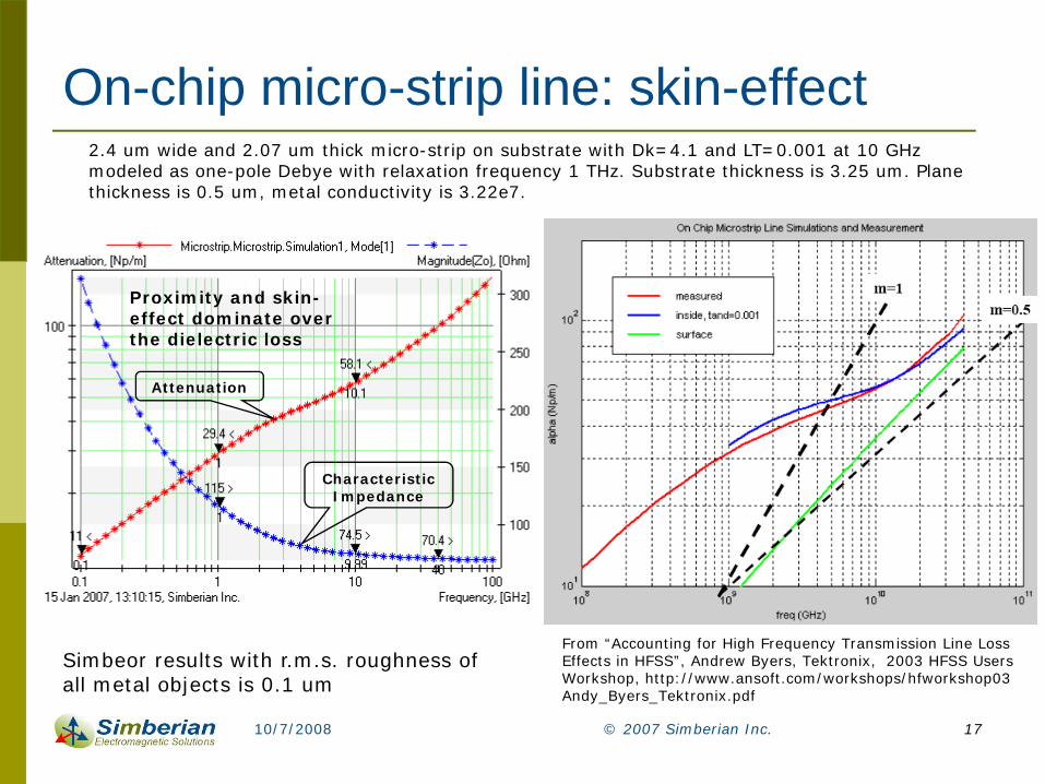
On-chip micro-strip line exampleExample: TLines\ Comparisons\ OnChip\ OnChip.esx2.4 um wide and 2.07 um thick micro-strip on substrate with Dk=4.1 and LT=0.001 at 10 GHz modeled as one-pole Debye with relaxation frequency 1 THz. Substrate thickness is 3.25 um. Plane thickness is 0.5 um, metal conductivity is 3.22e7.
10/7/2008 © 2007 Simberian Inc. 17
On-chip micro-strip line: skin-effect
Simbeor results with r.m.s. roughness of all metal objects is 0.1 um
2.4 um wide and 2.07 um thick micro-strip on substrate with Dk=4.1 and LT=0.001 at 10 GHz modeled as one-pole Debye with relaxation frequency 1 THz. Substrate thickness is 3.25 um. Plane thickness is 0.5 um, metal conductivity is 3.22e7.
Proximity and skin-effect dominate over the dielectric loss
Characteristic Impedance
Attenuation
From “Accounting for High Frequency Transmission Line Loss Effects in HFSS”, Andrew Byers, Tektronix, 2003 HFSS Users Workshop, http://www.ansoft.com/workshops/hfworkshop03 Andy_Byers_Tektronix.pdf

10/7/2008 © 2007 Simberian Inc. 18
Domination of the skin-effect over dielectric loss for the on-chip micro-strip line
2.4 um wide and 2.07 um thick micro-strip on substrate with Dk=4.1 and LT=0.001 at 10 GHz modeled as one-pole Debye with relaxation frequency 1 THz. Substrate thickness is 3.25 um. Plane thickness is 0.5 um, metal conductivity is 3.22e7.
Dielectric loss only
Inductance p.u.l.
Resistance p.u.l.
Metal only and total losses

10/7/2008 © 2007 Simberian Inc. 19
Microwave IC (MIC) micro-strip line example
1) F.J. Schmuckle, R. Pregla, "The method of lines for the analysis of lossy planar waveguides", IEEE Trans. on MTT, v. 38, 1990, N 10, p. 1473-1479.2) R.A. Pucel, D.J. Masse, C.P. Hartwig, "Losses in microstrip", IEEE Trans. on MTT, vol. 16, 1968, N 6, p. 342-350.
Microstrip line: Blue curves – attenuation and impedance with flat metal surfaces, red curves with metal surface roughness 0.5 um.
© 1990 by IEEE
Example: TLines\ AttenuationTest1\ AttenuationTest1.esx
10/7/2008 © 2007 Simberian Inc. 20
ConclusionAnalysis of signal propagation in multilayered interconnects requires 3D full-wave models for transmission lines in case if
Models valid over 5-6 frequency decades are required (multi-gigabit serial data channels)Polarization and high-frequency dispersion effects have to be taken into accountRoughness effects have to be taken into accountConductor plating effects have to be taken into account
Simplified electromagnetic and static models may be not correct and result in the design failure, project delays, increased cost …

Solutions and contactsAll solution files for these notes are available in My Documents/Simbeor Solutions directory after installation of Simbeor 2007Send questions and comments to
General: [email protected]: [email protected]: [email protected]
Web site www.simberian.com
10/7/2008 © 2007 Simberian Inc. 21