2-Stage 4-Phase Switched-Capacitor Boost DC-AC Inverter ...
6
Abstract— A new closed-loop scheme of 2-stage 4-phase switched-capacitor (SC) boost DC-AC inverter is proposed by combining 4-phase phase generator and sinusoidal pulse -frequency-modulation (SPFM) controller for low-power step-up inversion and regulation. In this SC inverter, the power part of the inverter is composed of 2-stage 4-phase SC booster and DC-link inverter. This SC booster contains 2 pumping capacitors and 4 switches operation for boosting the step-up gain up to 2 2 = 4 at most. For improving total harmonic distortion (THD), a 4x/3x/2x/1x selector is presented to select a proper gain in order to make the maximum of the practical output close to the desired output voltage as much as possible. The DC-link inverter like H-bridge structure consists of 4 switches controlled by SPFM to realize full-wave DC-AC operation. Besides, the SPFM is employed for the closed-loop realization to enhance the output realization capability for the different output peak and frequency. Finally, the 2-stage 4-phase SC boost inverter is simulated by OrCAD, and all results are illustrated to show the efficacy of the proposed scheme. Index Terms— switched-capacitor (SC), boost DC-AC inverter, sinusoidal pulse-frequency-modulation (SPFM). I. INTRODUCTION ith the popularity of portable electronic equipments, e.g. digital camera, e-book, mobile phone, notebook, and pad …etc., the power modules of these products always ask for some good characteristics: small volume, light weight, higher efficiency, and better regulation capability. Generally, the traditional power converters have a large volume and a heavy weight because of magnetic elements. Therefore, more manufactures and researchers pay much attention to this topic, and ultimately, requiring DC-DC/DC-AC converters realized on a compact chip by mixed-mode VLSI technology. The switched-capacitor (SC) power converter has received more and more attention because it has only semiconductor switches and capacitors. Thus, this kind of SC converters is one of the good solutions for low-power DC-DC/DC-AC conversion. Unlike the traditional converter, the SC converter needs no magnetic element, so they always have the small volume and light weight. The SC converter is usually designed for an output higher than supply voltage or a reverse-polarity voltage. This function fits many applications, e.g. drivers of electromagnetic luminescent (EL) lamp, white light emitting diode (WLED), op-amp, and LCD drivers. Up to now, the various SC types have been suggested for power conversion. In 1990, the first SC step-down converters were proposed by Japan researchers [1], and their idea is to switch MOSFETS cyclically according to 4 periods of capacitors charging/discharging for step-down conversion. In 1993, Cheong et al. suggested a modified SC converter with two symmetrical SC cells working in the two periods [2]. In 1995, Chung and Ioinovici suggested a current-mode SC for improving current waveforms [3]. In 1998, Mak and Ioinovici suggested an SC inverter with high power density [4]. In 2004, Chang proposed design and analysis of power-CMOS-gate-based SC boost DC-AC inverter [5]. The advantage of this SC inverter is to reduce the electromagnetic interference (EMI) problem. In 2007, Chang proposed CPLD-based closed-loop implementation of SC step-down DC-DC converter for multiple output choices [6]. In 2010, Hinago and Koizumi proposed a single-phase multilevel inverter using switched series/parallel DC voltage sources based on multiple independent voltage sources in order to reach the higher number of levels so as to reduce the THD value [7]. In 2011, Chang proposed an integrated SC step-up/down DC-DC/DC-AC converter/inverter [8-11]. In this paper, by using the 2-stage 4-phase SC boost and SPFM control, the boost DC-AC inverter is proposed not only to enhance full-wave output regulation via SPFM technique, but also to improve the THD value and provide the maximum gain proportional to the number of pumping capacitors. II. CONFIGURATION Fig.1 shows the configuration of the 2-stage 4-phase SC boost DC-AC inverter proposed, and it contains two parts: power part and control part. The discussions are as follow. A. Power Part This SC boost inverter as in the upper of Fig. 1 is composed of a 2-stage 4-phase booster and a DC-link inverter for DC-AC conversion. The 2-stage 4-phase booster consists of four switches (S1-S4) and two pumping capacitors (C1, C2) between supply source Vs and DC-link inverter, where each pumping capacitor is assumed with the same value C (C1=C2=C). The main function of this booster is to obtain a voltage up to 4×, 3×, 2×, and 1× the voltage of Vs, and then DC-link inverter is to invert this voltage for reaching the sinusoidal output. Thus, this power part can provide the output range of +4Vs ~ -4Vs for realizing DC-AC conversion. Fig. 2 shows the theoretical waveforms of these switches S1-S4, Sa, Sb, and V out. These operations are discussed below. 2-Stage 4-Phase Switched-Capacitor Boost DC-AC Inverter with Sinusoidal PFM Control Yuen-Haw Chang, Chin-Ling Chen, and Po-Chien Lo W Manuscript received December 5, 2013. This work is supported in part by the National Science Council of Taiwan, R.O.C., under Grant NSC 102-2221-E-324-030. Yuen-Haw Chang, Chin-Ling Chen, and Po-Chien Lo are with the Department and Graduate Institute of Computer Science and Information Engineering, Chaoyang University of Technology, Taichung, Taiwan, R.O.C. Post code: 413. (e-mail: [email protected] , [email protected], [email protected] ). Proceedings of the International MultiConference of Engineers and Computer Scientists 2014 Vol II, IMECS 2014, March 12 - 14, 2014, Hong Kong ISBN: 978-988-19253-3-6 ISSN: 2078-0958 (Print); ISSN: 2078-0966 (Online) IMECS 2014
Transcript of 2-Stage 4-Phase Switched-Capacitor Boost DC-AC Inverter ...
Abstract— A new closed-loop scheme of 2-stage 4-phase
switched-capacitor (SC) boost DC-AC inverter is proposed by combining 4-phase phase generator and sinusoidal pulse -frequency-modulation (SPFM) controller for low-power step-up inversion and regulation. In this SC inverter, the power part of the inverter is composed of 2-stage 4-phase SC booster and DC-link inverter. This SC booster contains 2 pumping capacitors and 4 switches operation for boosting the step-up gain up to 22 = 4 at most. For improving total harmonic distortion (THD), a 4x/3x/2x/1x selector is presented to select a proper gain in order to make the maximum of the practical output close to the desired output voltage as much as possible. The DC-link inverter like H-bridge structure consists of 4 switches controlled by SPFM to realize full-wave DC-AC operation. Besides, the SPFM is employed for the closed-loop realization to enhance the output realization capability for the different output peak and frequency. Finally, the 2-stage 4-phase SC boost inverter is simulated by OrCAD, and all results are illustrated to show the efficacy of the proposed scheme.
Index Terms— switched-capacitor (SC), boost DC-AC inverter, sinusoidal pulse-frequency-modulation (SPFM).
I. INTRODUCTION ith the popularity of portable electronic equipments, e.g. digital camera, e-book, mobile phone, notebook,
and pad …etc., the power modules of these products always ask for some good characteristics: small volume, light weight, higher efficiency, and better regulation capability. Generally, the traditional power converters have a large volume and a heavy weight because of magnetic elements. Therefore, more manufactures and researchers pay much attention to this topic, and ultimately, requiring DC-DC/DC-AC converters realized on a compact chip by mixed-mode VLSI technology.
The switched-capacitor (SC) power converter has received more and more attention because it has only semiconductor switches and capacitors. Thus, this kind of SC converters is one of the good solutions for low-power DC-DC/DC-AC conversion. Unlike the traditional converter, the SC converter needs no magnetic element, so they always have the small volume and light weight. The SC converter is usually designed for an output higher than supply voltage or a reverse-polarity voltage. This function fits many applications, e.g. drivers of electromagnetic luminescent (EL) lamp, white
light emitting diode (WLED), op-amp, and LCD drivers. Up to now, the various SC types have been suggested for power conversion. In 1990, the first SC step-down converters were proposed by Japan researchers [1], and their idea is to switch MOSFETS cyclically according to 4 periods of capacitors charging/discharging for step-down conversion. In 1993, Cheong et al. suggested a modified SC converter with two symmetrical SC cells working in the two periods [2]. In 1995, Chung and Ioinovici suggested a current-mode SC for improving current waveforms [3]. In 1998, Mak and Ioinovici suggested an SC inverter with high power density [4]. In 2004, Chang proposed design and analysis of power-CMOS-gate-based SC boost DC-AC inverter [5]. The advantage of this SC inverter is to reduce the electromagnetic interference (EMI) problem. In 2007, Chang proposed CPLD-based closed-loop implementation of SC step-down DC-DC converter for multiple output choices [6]. In 2010, Hinago and Koizumi proposed a single-phase multilevel inverter using switched series/parallel DC voltage sources based on multiple independent voltage sources in order to reach the higher number of levels so as to reduce the THD value [7]. In 2011, Chang proposed an integrated SC step-up/down DC-DC/DC-AC converter/inverter [8-11].
In this paper, by using the 2-stage 4-phase SC boost and SPFM control, the boost DC-AC inverter is proposed not only to enhance full-wave output regulation via SPFM technique, but also to improve the THD value and provide the maximum gain proportional to the number of pumping capacitors.
II. CONFIGURATION Fig.1 shows the configuration of the 2-stage 4-phase SC
boost DC-AC inverter proposed, and it contains two parts: power part and control part. The discussions are as follow.
A. Power Part This SC boost inverter as in the upper of Fig. 1 is composed
of a 2-stage 4-phase booster and a DC-link inverter for DC-AC conversion. The 2-stage 4-phase booster consists of four switches (S1-S4) and two pumping capacitors (C1, C2) between supply source Vs and DC-link inverter, where each pumping capacitor is assumed with the same value C (C1=C2=C). The main function of this booster is to obtain a voltage up to 4×, 3×, 2×, and 1× the voltage of Vs, and then DC-link inverter is to invert this voltage for reaching the sinusoidal output. Thus, this power part can provide the output range of +4Vs ~ -4Vs for realizing DC-AC conversion. Fig. 2 shows the theoretical waveforms of these switches S1-S4, Sa, Sb, and Vout. These operations are discussed below.
2-Stage 4-Phase Switched-Capacitor Boost DC-AC Inverter with Sinusoidal PFM Control
Yuen-Haw Chang, Chin-Ling Chen, and Po-Chien Lo
W
Manuscript received December 5, 2013. This work is supported in part by the National Science Council of Taiwan, R.O.C., under Grant NSC 102-2221-E-324-030.
Yuen-Haw Chang, Chin-Ling Chen, and Po-Chien Lo are with the Department and Graduate Institute of Computer Science and Information Engineering, Chaoyang University of Technology, Taichung, Taiwan, R.O.C. Post code: 413. (e-mail: [email protected], [email protected], [email protected]).
Proceedings of the International MultiConference of Engineers and Computer Scientists 2014 Vol II, IMECS 2014, March 12 - 14, 2014, Hong Kong
ISBN: 978-988-19253-3-6 ISSN: 2078-0958 (Print); ISSN: 2078-0966 (Online)
IMECS 2014

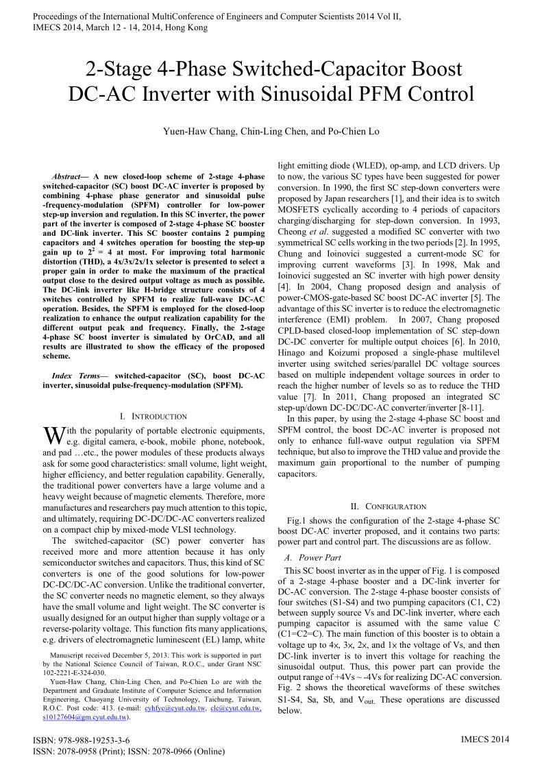
1) Positive Half-Wave (PHW):
a) Phase I: S1, S2 turn on, and S3, S4, Sa, Sb turn off. The
relevant topology is shown in Fig. 3(a). C1, C2 are charged by Vs in parallel.
b) Phase II:
S2, S3 turn on, and S1, S4, Sa, Sb turn off. The relevant topology is shown in Fig. 3(b). C2 is charged by Vs and C1 in series.
c) Phase III:
S1 turns on, and S2, S3, S4, Sa, Sb turn off. The relevant topology is shown in Fig. 3(c).The only C1 is charged by Vs.
d) Phase IV:
In the PHW for various voltage gains (4×, 3×, 2×, 1×), the different phase IV operations (switches and topologies) are explained below.
(i) 4×:
S3, S4, Sa, turn on, and S1, S2, Sb turn off. The current flow is passing from Vs, C1, and C2 in series connection through S3, S4 to the DC-link as in Fig. 3(d). And with the help of Sa, the positive 4× function can be achieved (Vout: ~ +4Vs).
(ii) 3×: S4, Sa turn on, and S1, S2, S3, Sb turn off.
The current flow is passing from Vs and C2 in series connection through S4 to the DC-link as in Fig. 3(e). And with the help of Sa, the positive 3× function can be achieved (Vout: ~ +3Vs).
(iii) 2×: S3, Sa turn on, and S1, S2, S4, Sb turn off.
The current flow is passing from Vs and C1 in series connection through S3 to the DC-link as in Fig. 3(f). And with the help of Sa, the positive 2× function can be achieved (Vout: ~ +2Vs).
(iv) 1×: Sb trun on, S1, S2, S3, S4, S3, Sb turn off.
The current flow is passing from Vs to the DC-link as in Fig. 3(g). And with the help of Sa, the positive 1× function can be achieved (Vout: ~ +1Vs).
2) Negative Half-Wave (NHW):
a) Phase I: S1, S2 turn on, and S3, S4, Sa, Sb turn off. The
relevant topology is shown in Fig. 3(a). C1, C2 are charged by Vs in parallel.
b) Phase II:
S2, S3 turn on, and S1, S4, Sa, Sb turn off. The relevant topology is shown in Fig. 3(b). C2 is charged by Vs and C1 in series.
Fig. 1. Configuration of closed-loop 2-stage 4-phase SC boost DC-AC inverter.
Proceedings of the International MultiConference of Engineers and Computer Scientists 2014 Vol II, IMECS 2014, March 12 - 14, 2014, Hong Kong
ISBN: 978-988-19253-3-6 ISSN: 2078-0958 (Print); ISSN: 2078-0966 (Online)
IMECS 2014

c) Phase III:
S1 turns on, and S2, S3, S4, Sa, Sb turn off. The relevant topology is shown in Fig. 3(c).The only C1 is charged by Vs.
d) Phase IV: In the NHW for various voltage gains (4×, 3×, 2×, 1
×), the different phase IV operations (switches and topologies) are explained below.
(i) 4×
S3, S4, Sb, turn on, and S1, S2, Sa turn off. The current flow is passing from Vs, C1, and C2 in series connection through S3, S4 to the DC-link as in Fig. 3(d). And with the help of Sb, the negative 4× function can be achieved (Vout: ~ -4Vs).
(ii) 3×: S4, Sb turn on, and S1, S2, S3, Sa turn off.
The current flow is passing from Vs and C2 in series connection through S4 to the DC-link as in Fig. 3(e). And with the help of Sb, the negative 3× function can be achieved (Vout: ~ -3Vs).
(iii) 2×: S3, Sb turn on, and S1, S2, S4, Sa turn off.
The current flow is passing from Vs and C1 in series connection through S3 to the DC-link as in Fig. 3(f). And with the help of Sb, the positive 2× function can be achieved (Vout: ~ -2Vs).
(iv) 1×: Sb turn on, S1, S2, S3, S4, Sa, Sb turn off.
The current flow is passing from Vs to the DC-link as in Fig. 3(g). And with the help of Sb, the positive 1× function can be achieved (Vout: ~ -1Vs).
B. Control Part In the proposed inverter, the SPFM-based controller is
used as shown in lower of Fig. 1. The controller is composed of SPFM block and phase generator. From the view of signal flow, Vout is firstly sent into the SPFM block. After the operation of absolute value, Vout is compared with the desired output signal Vref (sinusoidal reference) to obtain a control signal Vc as:
If |Vref|≧|Vout|, then Vc =1, If |Vref|<|Vout|, then Vc =0.
Next, according to Vc and |Vref|, the 4x/3x/2x/1x selector as in Fig. 4 can generate the boosting control signals (S24, S34) for a proper gain level, and the relevant rules are shown as below: 1) If |Vref| ≧ Vdd and Vc =0, then S24 =0, S34 =0;
2) If |Vref| ≧ Vdd and Vc =1, then S24 =1, S34 =1;
3) If Vdd≦ |Vref|< Vdd and Vc =0, then S24 =0, S34 =0;
4) If Vdd≦ |Vref|< Vdd and Vc =1, then S24 =0, S34 =1;
5) If Vdd≦ |Vref|< Vdd and Vc =0, then S24 =0, S34 =0;
Fig. 2. Theoretical waveforms of the proposed inverter.
Proceedings of the International MultiConference of Engineers and Computer Scientists 2014 Vol II, IMECS 2014, March 12 - 14, 2014, Hong Kong
ISBN: 978-988-19253-3-6 ISSN: 2078-0958 (Print); ISSN: 2078-0966 (Online)
IMECS 2014
6) If Vdd≦ |Vref|< Vdd and Vc =1, then S24 =1, S34 =0;
7) If 0V≦ |Vref|< Vdd and Vc =0, then S24 =0, S34 =0;
8) If 0V≦ |Vref|< Vdd and Vc =1, then S24 =0, S34 =0.
With the digital logic gates, the phase generator can be easily designed to obtain a set of nonoverlapping complementary signalsψ1 andψ2. Based onψ1 andψ2, the switch signals S1-S4, Sa and Sb can be operated just like the waveforms in Fig. 2, where the frequency ofψ11 is exactly half of that of ψ1 , andψ12 is the antiphase signal of ψ11. Here, all detailed Boolean relationships of S1-S4, Sa and Sb are shown as follows: (“‧”: logic AND). S1=ψ1 , S2=ψ11 , S3= ψ2‧S24 ,
Fig. 4. 4x/3x/2x/1x selector control circuit.
(f)
(g)
Fig. 3. Topologies of the proposed inverter for (a) Phase I, (b) Phase II, (c) Phase III, (d) Phase IV of 4x, (e) Phase IV of 3x, (f) Phase IV of 2x, and (g) Phase IV of 1x.
(a)
(b)
(c)
(d)
(e)
Proceedings of the International MultiConference of Engineers and Computer Scientists 2014 Vol II, IMECS 2014, March 12 - 14, 2014, Hong Kong
ISBN: 978-988-19253-3-6 ISSN: 2078-0958 (Print); ISSN: 2078-0966 (Online)
IMECS 2014
S4= ψ2‧ψ12‧S34 , Sa= ψ2‧ψ12‧S+
‧Vc , Sb= ψ2‧ψ12‧S-
‧Vc . The goal is to generate these SPFM control signals S1-S4, Sa and Sb for realizing phase I- IV topologies as in Fig. 3.
III. EXAMPLES In this paper, the 2-stage 4-phase SC boost inverter is
simulated by OrCAD, and then the results are illustrated to verify the efficacy of the proposed inverter. All the parameters are listed in Table I. There are 3 cases (fo=1.2 kHz, 1 kHz, and 0.8 kHz), each including two different Vm, to be discussed as follows.
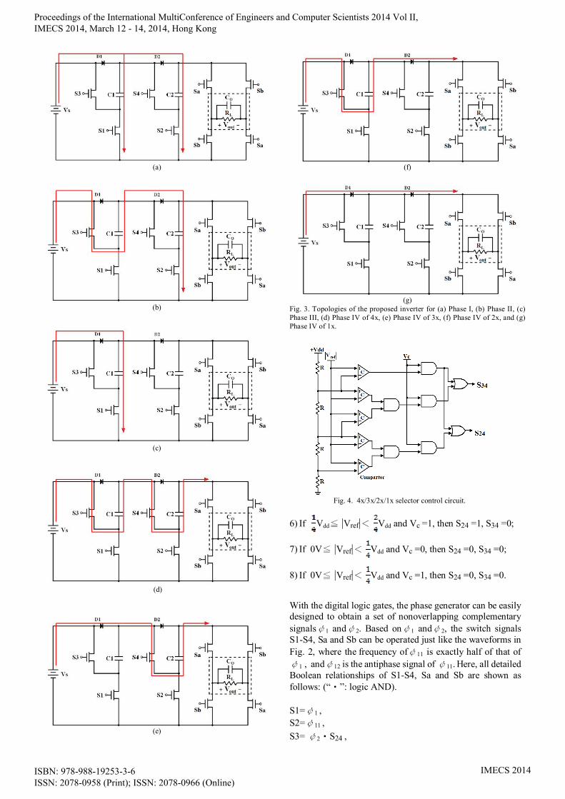
1) Case 1: fo=1.2 kHz
a) Vm=18.9V: Let the supply source Vs be DC 5V, load RL be
500Ω, and the peak value and output frequency of Vref are Vm=18.9V, fo=1.2kHz. The waveform of Vout is obtained as in Fig. 5(a). Vout has the peak value of 18.88V, and the practical output frequency is about 1.2 kHz. The efficiency is 77%, and THD is 4%.
b) Vm=14V: Let the supply source Vs be DC 5V, load RL be
500Ω, and the peak value and output frequency of Vref are Vm=14V, fo=1.2kHz. The waveform of Vout
(a)
(b)
(c)
(d)
(e)
(f)
Fig. 5. Output Vout for Vref: (a) Vm=18.9V, fo=1.2kHZ, (b) Vm=14V, fo=1.2kHZ, (c) Vm=18.9V, fo=1kHZ, (d) Vm=14V, fo=1kHZ, (e) Vm=18.9V, fo=0.8kHZ and (f) Vm=14V, fo=0.8kHZ.
20V
-20V
0V
20V
0V
-20V
20V
0V
-20V
20V
0V
-20V
20V
0V
-20V
20V
0V
-20V
10.0m s
10.0m s
10.0m s
10.0m s
10.0m s
10.0m s
Proceedings of the International MultiConference of Engineers and Computer Scientists 2014 Vol II, IMECS 2014, March 12 - 14, 2014, Hong Kong
ISBN: 978-988-19253-3-6 ISSN: 2078-0958 (Print); ISSN: 2078-0966 (Online)
IMECS 2014
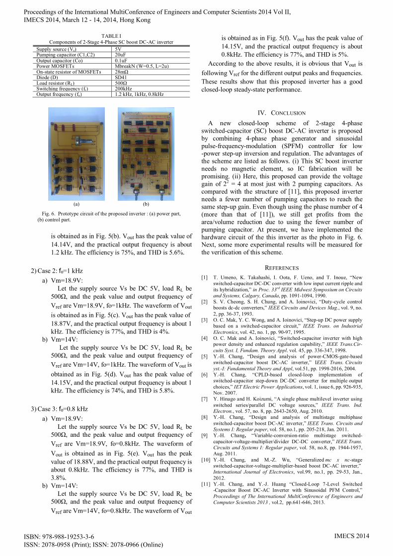
TABLE I Components of 2-Stage 4-Phase SC boost DC-AC inverter
Supply source (Vs) 5V Pumping capacitor (C1,C2) 20uF Output capacitor (Co) 0.1uF Power MOSFETs MbreakN (W=0.5, L=2u) On-state resistor of MOSFETs 28mΩ Diode (D) SD41 Load resistor (RL) 500Ω Switching frequency (fs) 200kHz
Output frequency (fo) 1.2 kHz, 1kHz, 0.8kHz
Fig. 6. Prototype circuit of the proposed inverter : (a) power part,
(b) control part.
is obtained as in Fig. 5(b). Vout has the peak value of 14.14V, and the practical output frequency is about 1.2 kHz. The efficiency is 75%, and THD is 5.6%.
2) Case 2: fo=1 kHz
a) Vm=18.9V: Let the supply source Vs be DC 5V, load RL be
500Ω, and the peak value and output frequency of Vref are Vm=18.9V, fo=1kHz. The waveform of Vout is obtained as in Fig. 5(c). Vout has the peak value of 18.87V, and the practical output frequency is about 1 kHz. The efficiency is 77%, and THD is 4%.
b) Vm=14V: Let the supply source Vs be DC 5V, load RL be
500Ω, and the peak value and output frequency of Vref are Vm=14V, fo=1kHz. The waveform of Vout is obtained as in Fig. 5(d). Vout has the peak value of 14.15V, and the practical output frequency is about 1 kHz. The efficiency is 74%, and THD is 5.8%.
3) Case 3: fo=0.8 kHz
a) Vm=18.9V: Let the supply source Vs be DC 5V, load RL be
500Ω, and the peak value and output frequency of Vref are Vm=18.9V, fo=0.8kHz. The waveform of Vout is obtained as in Fig. 5(e). Vout has the peak value of 18.88V, and the practical output frequency is about 0.8kHz. The efficiency is 77%, and THD is 3.8%.
b) Vm=14V: Let the supply source Vs be DC 5V, load RL be
500Ω, and the peak value and output frequency of Vref are Vm=14V, fo=0.8kHz. The waveform of Vout
is obtained as in Fig. 5(f). Vout has the peak value of 14.15V, and the practical output frequency is about 0.8kHz. The efficiency is 77%, and THD is 5%.
According to the above results, it is obvious that Vout is following Vref for the different output peaks and frequencies. These results show that this proposed inverter has a good closed-loop steady-state performance.
IV. CONCLUSION A new closed-loop scheme of 2-stage 4-phase
switched-capacitor (SC) boost DC-AC inverter is proposed by combining 4-phase phase generator and sinusoidal pulse-frequency-modulation (SPFM) controller for low -power step-up inversion and regulation. The advantages of the scheme are listed as follows. (i) This SC boost inverter needs no magnetic element, so IC fabrication will be promising. (ii) Here, this proposed can provide the voltage gain of 22 = 4 at most just with 2 pumping capacitors. As compared with the structure of [11], this proposed inverter needs a fewer number of pumping capacitors to reach the same step-up gain. Even though using the phase number of 4 (more than that of [11]), we still get profits from the area/volume reduction due to using the fewer number of pumping capacitor. At present, we have implemented the hardware circuit of the this inverter as the photo in Fig. 6. Next, some more experimental results will be measured for the verification of this scheme.
REFERENCES [1] T. Umeno, K. Takahashi, I. Oota, F. Ueno, and T. Inoue, “New
switched-capacitor DC-DC converter with low input current ripple and its hybridization,” in Proc. 33rd IEEE Midwest Symposium on Circuits and Systems, Calgary, Canada, pp. 1091-1094, 1990.
[2] S. V. Cheong, S. H. Chung, and A. Ioinovici, “Duty-cycle control boosts dc-dc converters,” IEEE Circuits and Devices Mag., vol. 9, no. 2, pp. 36-37, 1993.
[3] O. C. Mak, Y. C. Wong, and A. Ioinovici, “Step-up DC power supply based on a switched-capacitor circuit,” IEEE Trans. on Industrial Electronics, vol. 42, no. 1, pp. 90-97, 1995.
[4] O. C. Mak and A. Ioinovici, “Switched-capacitor inverter with high power density and enhanced regulation capability,” IEEE Trans.Cir- cuits Syst. I, Fundam. Theory Appl. vol. 45, pp. 336-347, 1998.
[5] Y.-H. Chang, “Design and analysis of power-CMOS-gate-based switched-capacitor boost DC-AC inverter,” IEEE Trans. Circuits yst.-I: Fundamental Theory and Appl, vol.51, pp. 1998-2016, 2004.
[6] Y.-H. Chang, “CPLD-based closed-loop implementation of switched-capacitor step-down DC-DC converter for multiple output choices,” IET Electric Power Applications, vol. 1, issue 6, pp. 926-935, Nov. 2007.
[7] Y. Hinago and H. Koizumi, “A single phase multilevel inverter using switched series/parallel DC voltage sources,” IEEE Trans. Ind. Electron., vol. 57, no. 8, pp. 2643-2650, Aug. 2010.
[8] Y.-H. Chang, “Design and analysis of multistage multiphase switched-capacitor boost DC-AC inverter,” IEEE Trans. Circuits and Systems I: Regular paper, vol. 58, no.1, pp. 205-218, Jan. 2011.
[9] Y.-H. Chang, “Variable-conversion-ratio multistage switched- capacitor-voltage-multiplier/divider DC-DC converter,” IEEE Trans. Circuits and Systems I: Regular paper, vol. 58, no.8, pp. 1944-1957, Aug. 2011.
[10] Y.-H. Chang, and M.-Z. Wu, “Generalized mc x nc-stage switched-capacitor-voltage-multiplier-based boost DC-AC inverter,” International Journal of Electronics, vol.99, no.1, pp. 29-53, Jan., 2012.
[11] Y.-H. Chang, and Y.-J. Huang “Closed-Loop 7-Level Switched -Capacitor Boost DC-AC Inverter with Sinusoidal PFM Control,” Proceedings of The International MultiConference of Engineers and Computer Scientists 2013 , vol.2, pp.641-646, 2013.
(b)
(a)
Proceedings of the International MultiConference of Engineers and Computer Scientists 2014 Vol II, IMECS 2014, March 12 - 14, 2014, Hong Kong
ISBN: 978-988-19253-3-6 ISSN: 2078-0958 (Print); ISSN: 2078-0966 (Online)
IMECS 2014