1992-8645 A NOVEL LOW POWER AND LOW DELAY BUFFER … · The N-stage buffer design has CMOS...
7
Journal of Theoretical and Applied Information Technology 31 st May 2017. Vol.95. No 10 © 2005 – ongoing JATIT & LLS ISSN: 1992-8645 www.jatit.org E-ISSN: 1817-3195 2132 A NOVEL LOW POWER AND LOW DELAY BUFFER USING DOMINO LOGIC DESIGN IN 32 NM TECHNOLOGY 1 M.SIVA KUMAR, 2 SANATH KUMAR TULASI, 3 SRAVANI KARANAM, 4 P.TEJDEEP, 5 A.NAGARJUNA, 6 K.SRISAIRAJVENKAT 1 ASSOC PROF, K L UNIVERSITY, Department of ECE, ANDHRAPRADESH, INDIA 2 ASST.PROF. K L UNIVERSITY, Department of ECE,ANDHRA PRADESH, INDIA 3,4,5 STUDENTS ,K L UNIVERSITY , Department of ECE,ANDHRA PRADESH, INDIA E-mail: 1 [email protected], 2 [email protected] , 3 [email protected], 4 [email protected] , 5 [email protected] , 6 [email protected] ABSTRACT As device dimensions are miniaturized, propagation delay and power optimization issues have been accelerating in the circuit design while driving large capacitive loads. Usually large fan out capacitive loads need to be driven by a single gate without compromising high speed. Just as scaling the delay in on-chip designs we go for a consistent system design to scale down the delay in off-chip designs also. So we focus mainly on driving that large capacitive loads , in this regard we introduce some driving circuits known as buffers .So the main objective of this paper is to minimize delay of the overall circuit and power consumption while driving large capacitive loads using buffers. Hence the work is carried out in tanner tool in 32 nm technology. Keywords: Adaptive Exon Predictor, Computational Complexity, Deoxyribonucleic Acid, Disease Identification, Exons, Three Base Periodicity 1. INTRODUCTION In the world of electronics and science the miniaturization of any substance plays a major role, therefore all the things that have to be embedded in a single chip. With this scenario came into existence a new technology known as VLSI. In the VLSI technology, Integrated circuits enabled today’s way of life. VLSI can be partitioned into digital and analog, in digital technology driving large capacitive loads at the output of circuit is a key issue in driving large capacitive loads are propagation delay and power dissipation, hence to drive the large amount of fan-out capacitive loads we need a series of CMOS inverters that can drive the large capacitive loads i.e a buffer that can drive large loads. The buffer can act as a temporary storage element and also as a unity gain amplifier .It can transform from high impedance state to low impedance state without any distortion. For these buffers, propagation delay and power optimization are predominant factors so as to develop buffers at a certain nanometer technologies as a result that can drive large capacitive loads and have minimum propagation delay and power optimization. 1.1. Load Capacitance: In order to analyze the performance of the inverter/buffer circuit we consider to drive the load with large capacitances and yet the same time obtain less delay as possible and ensure that power consumed is also less. In order to drive a strong load capacitance the size of the driver need to be large, for it is directly proportional to its gate capacitance to drive the load. Consequently a medium size inverter/buffer is required to drive the large inverter/buffer. An obvious solution to drive a large load is the use CMOS inverter chain/buffer.[1] Fig: 1.1 CMOS Inverter More propagation time is taken by the circuit in Fig: 1.1 to charge and discharge the capacitor, where as an
Transcript of 1992-8645 A NOVEL LOW POWER AND LOW DELAY BUFFER … · The N-stage buffer design has CMOS...

Journal of Theoretical and Applied Information Technology 31st May 2017. Vol.95. No 10
© 2005 – ongoing JATIT & LLS
ISSN: 1992-8645 www.jatit.org E-ISSN: 1817-3195
2132
A NOVEL LOW POWER AND LOW DELAY BUFFER USING
DOMINO LOGIC DESIGN IN 32 NM TECHNOLOGY
1M.SIVA KUMAR,
2SANATH KUMAR TULASI,
3SRAVANI KARANAM,
4P.TEJDEEP,
5A.NAGARJUNA,
6K.SRISAIRAJVENKAT
1ASSOC PROF, K L UNIVERSITY, Department of ECE, ANDHRAPRADESH, INDIA 2ASST.PROF. K L UNIVERSITY, Department of ECE,ANDHRA PRADESH, INDIA
3,4,5
STUDENTS ,K L UNIVERSITY , Department of ECE,ANDHRA PRADESH, INDIA
E-mail: [email protected],
ABSTRACT
As device dimensions are miniaturized, propagation delay and power optimization issues have been accelerating
in the circuit design while driving large capacitive loads. Usually large fan out capacitive loads need to be
driven by a single gate without compromising high speed. Just as scaling the delay in on-chip designs we go for
a consistent system design to scale down the delay in off-chip designs also. So we focus mainly on driving that
large capacitive loads , in this regard we introduce some driving circuits known as buffers .So the main
objective of this paper is to minimize delay of the overall circuit and power consumption while driving large
capacitive loads using buffers. Hence the work is carried out in tanner tool in 32 nm technology.
Keywords: Adaptive Exon Predictor, Computational Complexity, Deoxyribonucleic Acid, Disease
Identification, Exons, Three Base Periodicity
1. INTRODUCTION
In the world of electronics and science the
miniaturization of any substance plays a major role,
therefore all the things that have to be embedded in a
single chip. With this scenario came into existence a
new technology known as VLSI. In the VLSI
technology, Integrated circuits enabled today’s way of
life. VLSI can be partitioned into digital and analog,
in digital technology driving large capacitive loads at
the output of circuit is a key issue in driving large
capacitive loads are propagation delay and power
dissipation, hence to drive the large amount of fan-out
capacitive loads we need a series of CMOS inverters
that can drive the large capacitive loads i.e a buffer
that can drive large loads. The buffer can act as a
temporary storage element and also as a unity gain
amplifier .It can transform from high impedance state
to low impedance state without any distortion. For
these buffers, propagation delay and power
optimization are predominant factors so as to develop
buffers at a certain nanometer technologies as a result
that can drive large capacitive loads and have
minimum propagation delay and power optimization.
1.1. Load Capacitance:
In order to analyze the performance of the
inverter/buffer circuit we consider to drive the load
with large capacitances and yet the same time obtain
less delay as possible and ensure that power
consumed is also less. In order to drive a strong load
capacitance the size of the driver need to be large, for
it is directly proportional to its gate capacitance to
drive the load. Consequently a medium size
inverter/buffer is required to drive the large
inverter/buffer. An obvious solution to drive a large
load is the use CMOS inverter chain/buffer.[1]
Fig: 1.1 CMOS Inverter
More propagation time is taken by the circuit in Fig:
1.1 to charge and discharge the capacitor, where as an
Journal of Theoretical and Applied Information Technology 31st May 2017. Vol.95. No 10
© 2005 – ongoing JATIT & LLS
ISSN: 1992-8645 www.jatit.org E-ISSN: 1817-3195
2133
extra inverter is placed to minimize the propagation
delay.
1.2. Propagation Delay
Any circuit is said to be well designed if its
delay of propagation τρ is as low as possible, i.e. how
fast the circuit responds to the change in the inputs.
τρ=( τρLH + τρHL )/2………………..(1.1)
Where τΡhl refers to the response time of the gate
from a logic low to logic high output transition and
τρLH refers to a logic high to logic low transition.
Fig: 1.2 Propagation Delay Vs Voltage
At the 50% transition points of the input and output
waveforms the delay is measured. The performance of
the circuit is increased on reducing the gate delay
which is directly proportional to the load capacitance,
the value of βn and is inversely proportional to the
supply voltage. Hence the capacitance of the load is to
be reduced while increasing the supply voltage and
width of the transistor in order to obtain an optimum
delay. But initially we have considered running the
load with large capacitances hence we go for a buffer
chain with N stages needed.
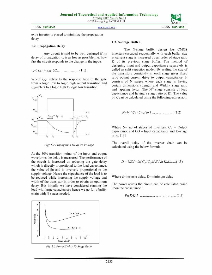
Fig:1.3.Power/Delay Vs Stage Ratio
1.3. N-Stage Buffer
The N-stage buffer design has CMOS
inverters cascaded sequentially with each buffer size
at current stage is increased by an order of stage ratio
K of its previous stage buffer. The method of
designing input and output capacitance separately is
called as split capacitor model. By scaling the size of
the transistors constantly in each stage gives fixed
ratio output current drive to output capacitance. It
consists of N stages where each stage is having
certain dimensions (Length and Width), stage ratio
and tapering factor. The Nth
stage consists of load
capacitance and having a stage ratio of Kn. The value
of K can be calculated using the following expression:
N=ln ( CN / CO )/ ln k ………………….(1.2)
Where N= no of stages of inverters, CN = Output
capacitance and CO = Input capacitance and K=stage
ratio. [12]
The overall delay of the inverter chain can be
calculated using the below formula:
D = NKd =ln( CN /CO )( K / ln K)d…….(1.3)
Where d=intrinsic delay, D=minimum delay
The power across the circuit can be calculated based
upon the capacitance :
Pα K/K-1 ………………………………(1.4)

Journal of Theoretical and Applied Information Technology 31st May 2017. Vol.95. No 10
© 2005 – ongoing JATIT & LLS
ISSN: 1992-8645 www.jatit.org E-ISSN: 1817-3195
2134
Fig: 1.4. N-Stage Buffer Along With Plot Between Delay Vs
Number Of Stages (N)
1.4. Conventional Buffer:
This section basically deals with
conventional 4 stage tapered buffer. It is a familiar
fact or thing that majority of the consumption of
power or power dissipation in electrical circuits
occurs due to the reason of charging and discharging
of CMOS .The short circuit power flows from Vdd to
Gnd during switching. The main thing about short
circuit power dissipation occurs in on chip or off chip
devices or switches. The conventional buffer contains
cascaded form of CMOS inverters in which follows
the concept of series of CMOS buffers built up in a
particular PMOS and NMOS format in a particular
nanometer technology. Based upon the load CL the
value of the delay can be varied. Here in this
conventional 4 stage buffer we use CL values such as
150pF, 289.3fF, 17.6fF and the tapering factor F as
1.5,3.0 that are designed for minimum delay.[5,6]
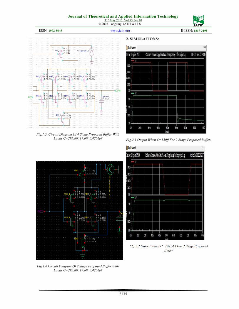
1.5. Proposed Buffer:
Same as the conventional buffer, proposed
buffer also has four stage tapered buffer. In CMOS
IC’s power dissipation and propagation delay is
caused by switching activity. The proposed buffer
gives less propagation delay and consumes less power
across load compared to conventional CMOS tapered
buffer but there will be more undesirable static power
dissipation. Its design is same as conventional tapered
buffer but an additional pre-charge logic is added.
Additional pre-charge logic is also known as Domino
logic or bypass circuitry logic. It is designed in tanner
tool with 32nm technology having certain dimensions
such as length and width pertaining to the related
technology. High speed logic circuits can be
implemented using Domino logic. An inverter is
added at the output of the dynamic gate in order to
complete the Domino logic. There are certain
advantages for considering Domino logic for the
proposed buffer design such as faster logic transition
speed and noise free operation. In contrast to the static
CMOS logic where both PMOS and NMOS must be
driven, only NMOS transistors need to be driven in
Domino logic also these inverters drive heavy loads
compared to the conventional CMOS logic. By
monitoring the inverter the speed of the Domino
circuits can be easily altered.
Fig.1.5.Flowchart Of The Proposed Buffer
Journal of Theoretical and Applied Information Technology 31st May 2017. Vol.95. No 10
© 2005 – ongoing JATIT & LLS
ISSN: 1992-8645 www.jatit.org E-ISSN: 1817-3195
2135
Fig.1.5. Circuit Diagram Of 4 Stage Proposed Buffer With
Loads C=295.8ff, 17.6ff, 0.4256pf
Fig.1.6.Circuit Diagram Of 2 Stage Proposed Buffer With
Loads C=295.8ff, 17.6ff, 0.4256pf
2. SIMULATIONS:
Fig.2.1 Output When C=150ff For 2 Stage Proposed Buffer.
Fig.2.2 Output When C=298.5Ff For 2 Stage Proposed
Buffer

Journal of Theoretical and Applied Information Technology 31st May 2017. Vol.95. No 10
© 2005 – ongoing JATIT & LLS
ISSN: 1992-8645 www.jatit.org E-ISSN: 1817-3195
2136
Fig.2.3 Output When C=0.4256pf For 2 Stage Proposed
Buffer.
Fig.2.4 Output When C=295.8ff For 4 Stage Proposed
Buffer
Fig. 2.5.Output When C=150 Pf For 4 Stage Proposed
Buffer
Fig.2.6. Output When C=17.6ff For 4 Stage Proposed
Buffers

Journal of Theoretical and Applied Information Technology 31st May 2017. Vol.95. No 10
© 2005 – ongoing JATIT & LLS
ISSN: 1992-8645 www.jatit.org E-ISSN: 1817-3195
2137
3.RESULTS
Table 2.1 Observed Results Of 2 Stage Tapered Buffer
Table 2.2.Observed Results Of 4 Stage Tapered Buffer
4. MERITS AND DEMERITS USING THIS
DOMINO LOGIC
1.Speed Advantages
2.Reduced fighting during transitions
3.Fewer transistors per gate, lower capacitive load
Area Advantages
Mainly consists of NMOS N+4 transistors instead of
2N transistors per gate.Therefore, domino logic is
widely in high performance circuit design.
1.All gates are non-inverting in nature.
2.Charge sharing, noise susceptibility.
3.Higher switching activity.
4.Need automated techniques considering these issues
for domino circuit design.
5. APPLICATIONS USING DOMINO LOGIC
i)It is used in large circuits, owing to its high
performance.
ii)Domino logic is widely used in custom circuit
design to achieve higher speed, smaller area and
potentially lower power consumption.
iii)As a consequence, a domino logic circuit can be
applicable such as high-speed adder, comparator and
arithmetic and logic unit (ALU) design
6. DISCUSSION ON RESULTS
The simulations are done using the tanner tools T-
SPICE in 32 nm technology and the circuits are
implemented. The width and the length of the
transistors are considered as 2.5um and 0.032um
respectively. The supply voltage Vdd is taken as 0.9
The simulations have been performed using domino
logic design along with the proposed one and are
compared with consideration of parameters such as
delay and power. The Table describes about the
power and delay measurements observed in the
proposed buffer circuit with that of the conventional
buffer circuit.
The proposed design in this paper has provided better
results with the power and delay parameters when
compared with the prior works. The values in the
Table represent the power measurements and the
delay measurements for the various domino styles.
The delay is sequentially decreased when compared
with the proposed design because of the high fan-out.
7. CONCLUSION:
In this paper the design of CMOS tapered buffer that
can drive large capacitive loads is simulated in tanner
tool (T-Spice &S-Spice) in 32nm technology .The
observations made between the conventional buffer
and proposed tapered buffer. From the observations
it can be concluded that the proposed buffer can drive
large capacitive loads compared to conventional
buffer with less propagation delay and power
dissipation.
Topology
CL(F)
N
FD
Vth
(V)
Static
Power
(watts)
Propagation
Delay
(seconds)
Conventio
nal Buffer
17.6f
2
5.0
6
2.5
75.09 p
10.099 n
Tapered
buffer
with
Feedback
network
17.6f 2 5.0
6
2.5 101.9 p 10.202 n
Proposed
Buffer
150f
0.4256p
295.8f
17.6f
2
2
2
2
1.5
1.5
1.5
1.5
0.9
0.9
0.9
0.9
99.9924 n
100.001 n
1.0272 n
3.434 n
20.886 n
8.3452 n
3.4336 n
s11.019 n
Topolo
gy
CL(F) N FD Vth
(V)
Static
Power
(watts)
Propagation
Delay
(seconds)
Conven
tional
tapered
Buffer
295.8 f
4
4.55
2.5
1.944 n
10.255 n
Conven
tional
tapered
Buffer
Domino
logic
295.8 f
4
4.55
2.5
1.945 n
10.224 n
Propose
d Buffer
17.6 f
0.4256
p
295.8 f
150 f
4
4
4
4
1.5
1.5
1.5
1.5
0.9
0.9
0.9
0.9
1.983 p
1.765 n
1.980 n
1.981 n
57.3298 p
23.345 n
27.295 p
2.8675 p

Journal of Theoretical and Applied Information Technology 31st May 2017. Vol.95. No 10
© 2005 – ongoing JATIT & LLS
ISSN: 1992-8645 www.jatit.org E-ISSN: 1817-3195
2138
8. FUTURE SCOPE
This project can be further extended using various
nano meter technologies such as
S22nm,14nm,10nm,7nm,5nm etc , and can use the
technology difference of power and delay like upon
scaling for various nano meter technologies the delay
and power values are also can be reduced that can be
proved. The 5nm technology is under renovation that
can come into existence in 2020. The work is carried
out using tanner tool and can further use cadence tool
also.
REFERENCES:
[1] Dinesh Sharma and Rajesh Mehra, “Low Power,
Delay Optimized Buffer Design using 70nm
CMOS Technology”, International Journal of
Computer Applications (0975 – 8887) Volume
22– No.3, May 2011
[2] Design of CMOS Tapered Buffer for High Speed
and Low Power Applications using 65nm
Technology,AnkurSaxena1,Payal Kaushik2
International Journal of Science and Research
(IJSR) ISSN (Online): 2319-7064 Index
Copernicus Value (2013): 6.14 | Impact Factor
(2013): 4.438.
[3] CMOS Buffer Design Approach for Low power
and Lower delay SRAM Design Mariyamol.p.
pa, Aswathy Nb*Global Colloquium in Recent
Advancement and Effectual Researches in
Engineering, Science and Technology
(RAEREST 2016).
[4] Novel Buffer Design for Low Power and Less
Delay in 45nm and 90nm Technology
Mahesha NB #1#1 Lecturer Department of
Electronics & Communication Engineering,
Rai Technology University.
[5] Multiple Threshold Voltage Design Scheme for
CMOS Tapered Buffers, Ahmed Shebaita and
Yehea Ismail, IEEE Transactions on Circuits
And Systems—II: Express Briefs, VOL. 55,
NO. 1, January 2008.
[6] Design of CMOS Tapered Buffer for High Speed
and Low Power Applications using 65nm
Technology, Ankur Saxena, Payal Kaushik,
International Journal of Science and Research
(IJSR) ISSN (Online): 2319-7064.
[7] Tapered-VTH CMOS Buffer Design for Improved
Energy Efficiency in Deep Nanometer
Technology, F Frustaci, P Corsonello, M Alioto
- Circuits and Systems ( …, 2011 -
ieeexplore.ieee.org
[8] Design of a sub threshold-supply bootstrapped
CMOS inverter based on an active leakage-
current reduction technique Y Ho, C Chang, C
Su - … Transactions on Circuits and Systems II:
…, 2012 - ieeexplore.ieee.org
[9] Design of Low Voltage and High-Speed BiCMOS
Buffer for Driving Large Load Capacitor I.J.
Engineering and Manufacturing, 2016, 1, 1-9
Published Online January 2016 in MECS
(http://www.mecspress.net)DOI:10.5815/ijem.2
016.01.01)
[10] A 65nm CMOS Pulse-Width-Controlled Driver
With 8Vpp Output Voltage For Switch-Mode
RF Pas Up To 3.6ghz Solid-State Circuits
Conference Digest Of Technical Papers
(ISSCC), 2011 IEEE International
10.1109/ISSCC.2011.5746218.
[11] Novel Dual-Threshold-Voltage Energy-Efficient
Buffers For Driving Large Extrinsic Load
Capacitance Circuits And Systems (ISCAS),
2013 IEEE International Symposium On
10.1109/ISCAS.2013.6572510.
[12] Gary Yeap . "Circuit", Practical Low Power
Digital VLSI Design, 1998.
[13] Design of Two-Stage Class AB CMOS Buffers: A
Systematic Approach Antonio Lopez Martin,
Jose Maria Algueta Algueta, Lucia Acosta,
Jaime Ramirez-Angulo, and Ramon Gonzalez
Carvajalvol June. 2011, pp. 393-400. IEEE
Journal of Solid-State Circuits ( Volume: 29,
Issue: 9, Sep 1994 )
[14] Tulasi Sanath Kumar,” Implementation and
Comparative analysis of 32-bit Low Power
Adiabatic & Hybrid Adders”. International
Journal of Recent Development in Engineering
and Technology, (ISSN 2347 - 6435 (Online))
Volume 3, Issue 1, July 2014.
[15] .Bisdounis, L. “Short-circuit energy dissipation
model for sub-100nm CMOS buffers”17th IEEE
International Conference on Electronics,
Circuits, and Systems (ICECS), Page(s): 615 -
618, 2010
[16] Lin Y, Zou X, Zheng Z, Huo W, Chen X, Kang
W. High-speed, Low Switching Noise and Load
Adaptive Output Buffer. Proceedings of the
International Symposium on Integrated Circuits
2009, (ISCI 2009), Singapore, 14-16; 280-282.