1/8 to 1/10 Duty LCD Display Drivers with Key Input … · 1/8 to 1/10 Duty LCD Display Drivers ......
39
Ordering number : ENN6370A 31000RM (OT)/12800RM No. 6370 -1/39 Overview The LC75808E and LC75808W are 1/8 to 1/10 duty LCD display drivers that can directly drive up to 600 segments and can control up to four general-purpose output ports. These products also incorporate a key scan circuit that accepts input from up to 30 keys to reduce printed circuit board wiring. Features • Key input function for up to 30 keys (A key scan is performed only when a key is pressed.) • 1/8duty–1/4bias, 1/9duty–1/4bias, and 1/10duty–1/4bias drive schemes can be controlled from serial data. 1/8duty–1/4bias: up to 480 segments 1/9duty–1/4bias: up to 540 segments 1/10duty–1/4bias: up to 600 segments • Sleep mode and all segments off functions that are controlled from serial data. • Serial data I/O supports CCB format communication with the system controller. • Direct display of display data without the use of a decoder provides high generality. • Built-in display contrast adjustment circuit. • Up to 4 general-purpose output ports are included. • Independent LCD driver block power supply V LCD . • Provision of an on-chip voltage-detection type reset circuit prevents incorrect displays. • The INH pin is provided. This pin turns off the display, disables key scanning, and forces the general-purpose output ports to the low level. • RC oscillator circuit. Package Dimensions unit: mm 3151-QFP100E unit: mm 3181B-SQFP100 21.6 0.8 3.0max 1.6 17.2 0.825 1 30 31 50 51 80 81 1.6 0.575 0.575 0.15 2.7 15.6 0.3 20.0 23.2 14.0 0.65 0.825 100 0.8 0.65 0.1 SANYO: QFP100E [LC75808E] 0.2 1.0 1.0 16.0 14.0 0.5 16.0 14.0 0.5 1.0 1.0 0.145 1.4 1.6max 0.5 0.5 100 1 25 26 50 51 75 76 0.1 SANYO: SQFP100 [LC75808W] LC75808E, 75808W SANYO Electric Co.,Ltd. Semiconductor Company TOKYO OFFICE Tokyo Bldg., 1-10, 1 Chome, Ueno, Taito-ku, TOKYO, 110-8534 JAPAN 1/8 to 1/10 Duty LCD Display Drivers with Key Input Function CMOS IC Any and all SANYO products described or contained herein do not have specifications that can handle applications that require extremely high levels of reliability, such as life-support systems, aircraft’s control systems, or other applications whose failure can be reasonably expected to result in serious physical and/or material damage. Consult with your SANYO representative nearest you before using any SANYO products described or contained herein in such applications. SANYO assumes no responsibility for equipment failures that result from using products at values that exceed, even momentarily, rated values (such as maximum ratings, operating condition ranges, or other parameters) listed in products specifications of any and all SANYO products described or contained herein. • CCB is a trademark of SANYO ELECTRIC CO., LTD. • CCB is SANYO’s original bus format and all the bus addresses are controlled by SANYO.
Transcript of 1/8 to 1/10 Duty LCD Display Drivers with Key Input … · 1/8 to 1/10 Duty LCD Display Drivers ......

Ordering number : ENN6370A
31000RM (OT)/12800RM No. 6370 -1/39
OverviewThe LC75808E and LC75808W are 1/8 to 1/10 duty LCD
display drivers that can directly drive up to 600 segmentsand can control up to four general-purpose output ports.These products also incorporate a key scan circuit thataccepts input from up to 30 keys to reduce printed circuitboard wiring.
Features• Key input function for up to 30 keys (A key scan is
performed only when a key is pressed.)• 1/8duty–1/4bias, 1/9duty–1/4bias, and 1/10duty–1/4bias
drive schemes can be controlled from serial data.1/8duty–1/4bias: up to 480 segments1/9duty–1/4bias: up to 540 segments1/10duty–1/4bias: up to 600 segments
• Sleep mode and all segments off functions that arecontrolled from serial data.
• Serial data I/O supports CCB format communicationwith the system controller.
• Direct display of display data without the use of adecoder provides high generality.
• Built-in display contrast adjustment circuit.• Up to 4 general-purpose output ports are included.• Independent LCD driver block power supply VLCD.• Provision of an on-chip voltage-detection type reset
circuit prevents incorrect displays.• The INH pin is provided. This pin turns off the display,
disables key scanning, and forces the general-purposeoutput ports to the low level.
• RC oscillator circuit.
Package Dimensionsunit: mm
3151-QFP100E
unit: mm
3181B-SQFP100
21.6 0.8
3.0m
ax
1.6
17.2
0.82
51 30
31
50
518081
1.60.5750.575 0.15
2.7
15.6
0.320.023.2
14.0
0.65
0.82
5100
0.8
0.65
0.1
SANYO: QFP100E
[LC75808E]
0.2
1.0
1.0
16.0
14.0
0.5
16.014.0
0.5 1.01.0 0.145
1.41.6m
ax
0.5 0.5
1001 25
26
50
5175
76
0.1
SANYO: SQFP100
[LC75808W]
LC75808E, 75808W
SANYO Electric Co.,Ltd. Semiconductor CompanyTOKYO OFFICE Tokyo Bldg., 1-10, 1 Chome, Ueno, Taito-ku, TOKYO, 110-8534 JAPAN
1/8 to 1/10 Duty LCD Display Drivers with Key Input Function
CMOS IC
Any and all SANYO products described or contained herein do not have specifications that can handleapplications that require extremely high levels of reliability, such as life-support systems, aircraft’scontrol systems, or other applications whose failure can be reasonably expected to result in seriousphysical and/or material damage. Consult with your SANYO representative nearest you before usingany SANYO products described or contained herein in such applications.
SANYO assumes no responsibility for equipment failures that result from using products at values thatexceed, even momentarily, rated values (such as maximum ratings, operating condition ranges, or otherparameters) listed in products specifications of any and all SANYO products described or containedherein.
• CCB is a trademark of SANYO ELECTRIC CO., LTD.
• CCB is SANYO’s original bus format and all the busaddresses are controlled by SANYO.
No. 6370 -2/39
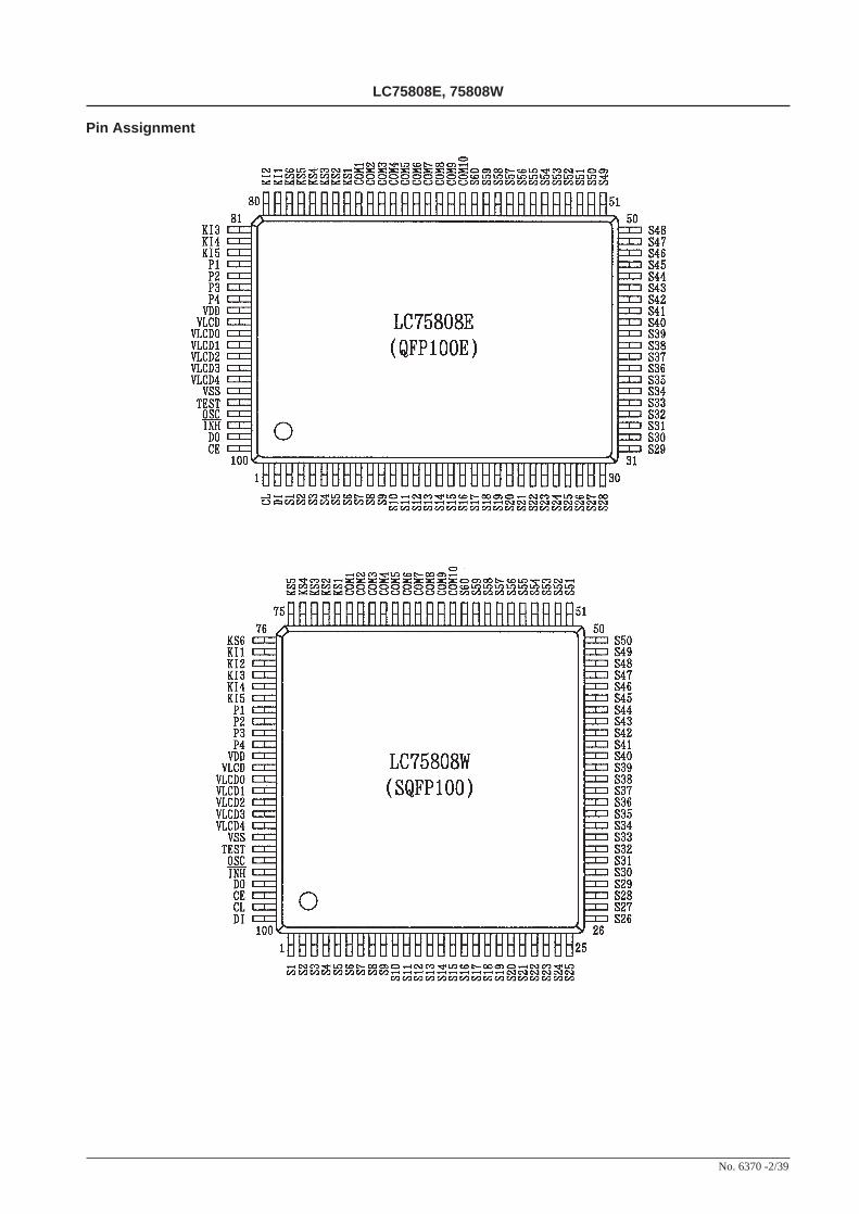
LC75808E, 75808W
Pin Assignment

No. 6370 -3/39
LC75808E, 75808W
Parameter Symbol Conditions Ratings Unit
Maximum supply voltageVDD max VDD –0.3 to +7.0 V
VLCD max VLCD –0.3 to +12.0
VIN1 CE, CL, DI, INH –0.3 to +7.0
Input voltage VIN2 OSC, KI1 to KI5, TEST –0.3 to VDD +0.3 V
VIN3 VLCD1, VLCD2, VLCD3, VLCD4 –0.3 to VLCD +0.3
VOUT1 DO –0.3 to +7.0
Output voltage VOUT2 OSC, KS1 to KS6, P1 to P4 –0.3 to VDD +0.3 V
VOUT3 VLCD0, S1 to S60, COM1 to COM10 –0.3 to VLCD +0.3
IOUT1 S1 to S60 300 µA
Output currentIOUT2 COM1 to COM10 3
IOUT3 KS1 to KS6 1 mA
IOUT4 P1 to P4 5
Allowable power dissipation Pd max Ta = 85°C 200 mW
Operating temperature Topr –40 to +85 °C
Storage temperature Tstg –55 to +125 °C
SpecificationsAbsolute Maximum Ratings at Ta=25°C, VSS=0V
Parameter Symbol ConditionsRatings
Unitmin typ max
VDD VDD 4.5 6.0
VLCD, When the display contrast adjustment 7.0 11.0Supply voltage
VLCDcircuit is used V
VLCD, When the display contrast adjustment 4.5 11.0circuit is not used
Output voltage VLCD0 VLCD0 VLCD4 + 4.5 VLCD V
VLCD1 VLCD13/4
VLCD0(VLCD0–VLCD4)
VLCD2 VLCD22/4
VLCD0Input voltage (VLCD0–VLCD4) V
VLCD3 VLCD31/4
VLCD0(VLCD0–VLCD4)
VLCD4 VLCD4 0 1.5
Input high level voltageVIH1 CE, CL, DI, INH 0.8 VDD 6.0
VVIH2 KI1 to KI5 0.6 VDD VDD
Input low level voltage VIL CE, CL, DI, INH, KI1 to KI5 0 0.2 VDD V
Recommended external resistance ROSC OSC 43 kΩ
Recommended external capacitance COSC OSC 680 pF
Guaranteed oscillation range fOSC OSC 25 50 100 kHz
Data setup time tds CL, DI :Figure 2 160 ns
Data hold time tdh CL, DI :Figure 2 160 ns
CE wait time tcp CE, CL :Figure 2 160 ns
CE setup time tcs CE, CL :Figure 2 160 ns
CE hold time tch CE, CL :Figure 2 160 ns
High level clock pulse width tøH CL :Figure 2 160 ns
Low level clock pulse width tøL CL :Figure 2 160 ns
DO output delay time tdc DO, RPU = 4.7 kΩ, CL = 10 pF *1 :Figure 2 1.5 µs
DO rise time tdr DO, RPU = 4.7 kΩ, CL = 10 pF *1 :Figure 2 1.5 µs
Allowable Operating Ranges at Ta = –40 to +85°C, VSS=0V
Note: *1. Since DO is an open-drain output, these values depend on the resistance of the pull-up resistor RPU and the load capacitance CL.

No. 6370 -4/39
LC75808E, 75808W
Parameter Symbol ConditionsRatings
Unitmin typ max
Hysteresis VH CE, CL, DI, INH, KI1 to KI5 0.1 VDD V
Power-down detection voltage VDET 2.5 3.0 3.5 V
Input high level current IIH CE, CL, DI, INH: VI = 6.0 V 5.0 µA
Input low level current IIL CE, CL, DI, INH: VI = 0 V –5.0 µA
Input floating voltage VIF KI1 to KI5 0.05 VDD V
Pull-down resistance RPD KI1 to KI5: VDD = 5.0 V 50 100 250 kΩ
Output off leakage current IOFFH DO: VO = 6.0 V 6.0 µA
VOH1 S1 to S60: IO = –20 µA VLCD0 – 0.6
Output high level voltageVOH2 COM1 to COM10: IO = –100 µA VLCD0 – 0.6
VVOH3 KS1 to KS6: IO = –500 µA VDD – 1.0 VDD – 0.5 VDD – 0.2
VOH4 P1 to P4: IO = –1 mA VDD – 1.0
VOL1 S1 to S60: IO = 20 µA VLCD4 + 0.6
VOL2 COM1 to COM10: IO = 100 µA VLCD4 + 0.6
Output low level voltage VOL3 KS1 to KS6: IO = 25 µA 0.2 0.5 1.5 V
VOL4 P1 to P4: IO = 1 mA 1.0
VOL5 DO: IO = 1mA 0.1 0.5
2/4 2/4VMID1 S1 to S60: IO = ±20 µA (VLCD0 – VLCD4) (VLCD0 – VLCD4)
–0.6 +0.6
3/4 3/4Output middle level voltage *2 VMID2 COM1 to COM10: IO = ±100 µA (VLCD0 – VLCD4) (VLCD0 – VLCD4) V
–0.6 +0.6
1/4 1/4VMID3 COM1 to COM10: IO = ±100 µA (VLCD0 – VLCD4) (VLCD0 – VLCD4)
–0.6 +0.6
Oscillator frequency fosc OSC: ROSC = 43 kΩ, COSC = 680 pF 40 50 60 kHz
IDD1 VDD :Sleep mode 100
IDD2 VDD: VDD = 6.0 V, outputs open,fosc = 50 kHz 250 500
ILCD1 VLCD : Sleep mode 5
VLCD : VLCD = 11.0 V
Current drain ILCD2Outputs open
500 1000 µAfosc = 50 kHz(When the display contrast adjustment circuit is used.)
VLCD : VLCD = 11.0 VOutputs open
ILCD3 fosc = 50 kHz 250 500(When the display contrast adjustment circuit is not used.)
Electrical Characteristics for the Allowable Operating Ranges
Note: *2. Excluding the bias voltage generation divider resistor built into VLCD0, VLCD1, VLCD2 , VLCD3, and VLCD4. (See Figure 1.)

No. 6370 -5/39
LC75808E, 75808W
Figure 1
1. When CL is stopped at the low level
Figure 2
2. When CL is stopped at the high level
To the common and segment drivers
Excluding these resistors.

No. 6370 -6/39
LC75808E, 75808W
Block Diagram

No. 6370 -7/39
LC75808E, 75808W
PinPin No.
Function Active I/O HandlingLC75808E LC75808W when unused
S1 to S60 3 to 62 1 to 60 Segment driver outputs. — OPEN
COM1 to COM10 72 to 63 70 to 61 Common driver outputs. — OPEN
KS1 to KS6 73 to 78 71 to 76 — O OPEN
KI1 to KI5 79 to 83 77 to 81Key scan inputs.
H I GNDThese pins have built-in pull-down resistors.
P1 to P4 84 to 87 82 to 85 General-purpose output ports. — OPEN
OSC 97 95 — I/O VDD
CE 100 98 H I
CL 1 99 I GND
DI 2 100 — I
DO 99 97 — O OPEN
INH 98 96 L I VDD
TEST 96 94 This pin must be connected to ground. — I —
VLCD0 90 88 — 0 OPEN
VLCD1 91 89 — I OPEN
VLCD2 92 90 — I OPEN
VLCD3 93 91 — I OPEN
VLCD4 94 92 — I GND
VDD 88 86 — — —
VLCD 89 87 — — —
VSS 95 93 Power supply connection. Connect to ground. — — —
Pin Functions
Key scan outputs.Although normal key scan timing lines require diodes to be inserted inthe timing lines to prevent shorts, since these outputs are unbalancedCMOS transistor outputs, these outputs will not be damaged by shortingwhen these outputs are used to form a key matrix.
Oscillator connection.An oscillator circuit is formed by connecting an external resistor andcapacitor at this pin.
Serial data interface connections to the controller. Note that DO, beingan open-drain output, requires a pull-up resistor.CE :Chip enableCL :Synchronization clockDI :Transfer dataDO :Output data
Input that turns the display off, disables key scanning, and forces thegeneral-purpose output ports low.• When INH is low (VSS):
• Display offS1 to S60 = “L” (VLCD4).COM1 to COM10 = “L” (VLCD4).
• General-purpose output ports P1 to P4 = low (VSS)• Key scanning is disabled: KS1 to KS6 = low (VSS)• All the key data is reset to low.
• When INH is high (VDD):• Display on• The states of the general-purpose output ports can be set by
the PC1 to PC4 control data.• Key scanning is enabled.
However, serial data can be transferred when the INH pin is low.
LCD drive 3/4 bias voltage (middle level) supply pin. This pin can beused to supply the 3/4 (VLCD0 – VLCD4) voltage level externally.
LCD drive 2/4 bias voltage (middle level) supply pin. This pin can beused to supply the 2/4 (VLCD0 – VLCD4) voltage level externally.
LCD drive 1/4 bias voltage (middle level) supply pin. This pin can beused to supply the 1/4 (VLCD0 – VLCD4) voltage level externally.
LCD drive 0/4 bias voltage (low level) supply pin. Fine adjustment of thedisplay contrast can be implemented by connecting an external variableresistor to this pin.However, (VLCD0 – VLCD4) must be greater than or equal to 4.5 V, andVLCD4 must be in the range 0 V to 1.5 V, inclusive.
Logic block power supply connection. Provide a voltage of between 4.5and 6.0V.
LCD driver block power supply connection. Provide a voltage of between7.0 and 11.0 V when the display contrast adjustment circuit is used andprovide a voltage of between 4.5 and 11.0 V when the circuit is not used.
LCD drive 4/4 bias voltage (high level) supply pin. The level on this pincan be changed by the display contrast adjustment circuit. However, (VLCD0 – VLCD4) must be greater than or equal to 4.5 V.Also,external power must not be applied to this pin since the pin circuitincludes the display contrast adjustment circuit.

No. 6370 -8/39
LC75808E, 75808W
Serial Data Input
1. 1/8 duty① When CL is stopped at the low level.
• When the display data is transferred.
• When the control data is transferred.
Note: B0 to B3,A0 to A3 ........ CCB addressDD................................ Direction data
Display data Fixed data
Display data Fixed data
Display data Fixed data
Display data Fixed data
Control data

No. 6370 -9/39
LC75808E, 75808W
② When CL is stopped at the high level.• When the display data is transferred.
Note: B0 to B3,A0 to A3 ........ CCB addressDD................................ Direction data
• CCB address: ....42H• D1 to D480: ........ Display data• KC1 to KC6: ........ Key scan output state setting data• PC1 to PC4: ........ General-purpose output port state setting data• CT0 to CT3, CTC: Display contrast setting data• SC: ...................... Segment on/off control data• SP: ...................... Normal mode/sleep mode control data• DT1, DT2: ............ Display technique setting data
• When the control data is transferred.
Control data
Display data Fixed data
Display data Fixed data
Display data Fixed data
Display data Fixed data

No. 6370 -10/39
LC75808E, 75808W
2. 1/9 duty① When CL is stopped at the low level.
• When the display data is transferred.
• When the control data is transferred.
Note: B0 to B3,A0 to A3 ........ CCB addressDD................................ Direction data
Display data Fixed data
Display data Fixed data
Display data
Fixed dataDisplay data
Fixed data
Control data

No. 6370 -11/39
LC75808E, 75808W
② When CL is stopped at the high level.• When the display data is transferred.
Note: B0 to B3,A0 to A3 ........ CCB addressDD................................ Direction data
• CCB address: ...... 42H• D1 to D540: ........ Display data• KC1 to KC6: ........ Key scan output state setting data• PC1 to PC4: ........ General-purpose output port state setting data• CT0 to CT3, CTC: Display contrast setting data• SC: ...................... Segment on/off control data• SP: ...................... Normal mode/sleep mode control data• DT1, DT2: ............ Display technique setting data
• When the control data is transferred.
Display data Fixed data
Display data
Fixed dataDisplay data
Fixed data
Display data Fixed data
Control data

No. 6370 -12/39
LC75808E, 75808W
3. 1/10 duty① When CL is stopped at the low level.
• When the display data is transferred.
• When the control data is transferred.
Note: B0 to B3,A0 to A3 ........ CCB addressDD................................ Direction data
Display data Fixed data
Display data Fixed data
Display data Fixed data
Display data Fixed data
Control data

No. 6370 -13/39
LC75808E, 75808W
② When CL is stopped at the high level.• When the display data is transferred.
Note: B0 to B3,A0 to A3 ........ CCB addressDD................................ Direction data
• CCB address: ...... 42H• D1 to D600: ........ Display data• KC1 to KC6: ........ Key scan output state setting data• PC1 to PC4: ........ General-purpose output port state setting data• CT0 to CT3, CTC: Display contrast setting data• SC: ...................... Segment on/off control data• SP: ...................... Normal mode/sleep mode control data• DT1, DT2: ............ Display technique setting data
• When the control data is transferred.
Display data Fixed data
Display data
Fixed data
Display data
Fixed data
Display data
Fixed data
Control data

No. 6370 -14/39
LC75808E, 75808W
Control Data Functions1. KC1 to KC6: Key scan output state setting data
These control data bits set the states of the key scan output pins KS1 to KS6.
For example, if KC1 to KC3 are set to 1, and KC4 to KC6 are set to 0, then the output pins KS1 to KS3 will output highlevels (VDD) and the output pins KS4 to KS6 will output low levels (VSS) in the key scan standby state.Note that key scan output signal is not output from output pins that are set low.
For example, if PC1 and PC2 are set to 1, and PC3 and PC4 are set to 0, then the output pins P1 and P2 will output highlevels (VDD) and the output pins P3 and P4 will output low levels (VSS).
Output pin KS1 KS2 KS3 KS4 KS5 KS6
Key scan output state setting data KC1 KC2 KC3 KC4 KC5 KC6
2. PC1 to PC4: General-purpose output port state setting dataThese control data bits set the states of the general-purpose output ports P1 to P4.
Output pin P1 P2 P3 P4
General-purpose output port state setting data PC1 PC2 PC3 PC4
3. CT0 to CT3, CTC: Display contrast setting dataThese control data bits set the display contrast.CT0 to CT3: Display contrast setting (11 steps)
CT0 CT1 CT2 CT3 LCD drive 4/4 bias voltage supply VLCD0 level
0 0 0 0 0.94 VLCD = VLCD – (0.03 VLCD × 2)
1 0 0 0 0.91 VLCD = VLCD – (0.03 VLCD × 3)
0 1 0 0 0.88 VLCD = VLCD – (0.03 VLCD × 4)
1 1 0 0 0.85 VLCD = VLCD – (0.03 VLCD × 5)
0 0 1 0 0.82 VLCD = VLCD – (0.03 VLCD × 6)
1 0 1 0 0.79 VLCD = VLCD – (0.03 VLCD × 7)
0 1 1 0 0.76 VLCD = VLCD – (0.03 VLCD × 8)
1 1 1 0 0.73 VLCD = VLCD – (0.03 VLCD × 9)
0 0 0 1 0.70 VLCD = VLCD – (0.03 VLCD × 10)
1 0 0 1 0.67 VLCD = VLCD – (0.03 VLCD × 11)
0 1 0 1 0.64 VLCD = VLCD – (0.03 VLCD × 12)
CTC: Display contrast adjustment circuit state setting
Note that although the display contrast can be adjusted by operating the built-in display contrast adjustment circuit, it isalso possible to apply fine adjustments to the contrast by connecting an external variable resistor to the VLCD4 pin andmodifying the VLCD4 pin voltage. However, the following conditions must be met: (VLCD0 – VLCD4) ≥ 4.5 V, and 1.5 V≥ VLCD4 ≥ 0 V.
CTC Display contrast adjustment circuit state
0 The display contrast adjustment circuit is disabled, and the VLCD0 pin level is forced to the VLCD level.
1 The display contrast adjustment circuit operates, and the display contrast is adjusted.

No. 6370 -15/39
LC75808E, 75808W
However, note that when the segments are turned off by setting SC to 1, the segments are turned off by outputting segment off waveforms from the segmentoutput pins.
Note: COMn (n = 9 or 10): Common outputs
SC Display state
0 On
1 Off
4. SC: Segment on/off control dataThis control data bit controls the on/off state of the segments.
SP Mode
0 Normal mode
Sleep mode
1 The common and segment pins go to the VLCD4 level and the oscillator on the OSC pin is stopped (although it operates during keyscan operations) to reduce current drain. Note that the states of the general-purpose output ports P1 to P4 are set by PC1 to PC4 inthe control data during sleep mode as well as normal mode.
5. SP: Normal mode/sleep mode control dataThis control data bit controls the normal mode and sleep mode.
6. DT1, DT2: Display technique setting dataThese control data bits set the display technique.
DT1 DT2 Display techniqueOutput pins
COM9 COM10
0 0 1/8 duty 1/4 bias drive Fixed at the VLCD4 level Fixed at the VLCD4 level
1 0 1/9 duty 1/4 bias drive COM9 Fixed at the VLCD4 level
0 1 1/10 duty 1/4 bias drive COM9 COM10

No. 6370 -16/39
LC75808E, 75808W
Display Data and Output Pin Correspondence1. 1/8 duty
Output Pin COM1 COM2 COM3 COM4 COM5 COM6 COM7 COM8
S1 D1 D2 D3 D4 D5 D6 D7 D8
S2 D9 D10 D11 D12 D13 D14 D15 D16
S3 D17 D18 D19 D20 D21 D22 D23 D24
S4 D25 D26 D27 D28 D29 D30 D31 D32
S5 D33 D34 D35 D36 D37 D38 D39 D40
S6 D41 D42 D43 D44 D45 D46 D47 D48
S7 D49 D50 D51 D52 D53 D54 D55 D56
S8 D57 D58 D59 D60 D61 D62 D63 D64
S9 D65 D66 D67 D68 D69 D70 D71 D72
S10 D73 D74 D75 D76 D77 D78 D79 D80
S11 D81 D82 D83 D84 D85 D86 D87 D88
S12 D89 D90 D91 D92 D93 D94 D95 D96
S13 D97 D98 D99 D100 D101 D102 D103 D104
S14 D105 D106 D107 D108 D109 D110 D111 D112
S15 D113 D114 D115 D116 D117 D118 D119 D120
S16 D121 D122 D123 D124 D125 D126 D127 D128
S17 D129 D130 D131 D132 D133 D134 D135 D136
S18 D137 D138 D139 D140 D141 D142 D143 D144
S19 D145 D146 D147 D148 D149 D150 D151 D152
S20 D153 D154 D155 D156 D157 D158 D159 D160
S21 D161 D162 D163 D164 D165 D166 D167 D168
S22 D169 D170 D171 D172 D173 D174 D175 D176
S23 D177 D178 D179 D180 D181 D182 D183 D184
S24 D185 D186 D187 D188 D189 D190 D191 D192
S25 D193 D194 D195 D196 D197 D198 D199 D200
S26 D201 D202 D203 D204 D205 D206 D207 D208
S27 D209 D210 D211 D212 D213 D214 D215 D216
S28 D217 D218 D219 D220 D221 D222 D223 D224
S29 D225 D226 D227 D228 D229 D230 D231 D232
S30 D233 D234 D235 D236 D237 D238 D239 D240
S31 D241 D242 D243 D244 D245 D246 D247 D248
S32 D249 D250 D251 D252 D253 D254 D255 D256
S33 D257 D258 D259 D260 D261 D262 D263 D264
S34 D265 D266 D267 D268 D269 D270 D271 D272
S35 D273 D274 D275 D276 D277 D278 D279 D280
S36 D281 D282 D283 D284 D285 D286 D287 D288
S37 D289 D290 D291 D292 D293 D294 D295 D296
S38 D297 D298 D299 D300 D301 D302 D303 D304
S39 D305 D306 D307 D308 D309 D310 D311 D312
S40 D313 D314 D315 D316 D317 D318 D319 D320
S41 D321 D322 D323 D324 D325 D326 D327 D328
S42 D329 D330 D331 D332 D333 D334 D335 D336
S43 D337 D338 D339 D340 D341 D342 D343 D344
S44 D345 D346 D347 D348 D349 D350 D351 D352
S45 D353 D354 D355 D356 D357 D358 D359 D360
Continued on next page.

No. 6370 -17/39
LC75808E, 75808W
Output Pin COM1 COM2 COM3 COM4 COM5 COM6 COM7 COM8
S46 D361 D362 D363 D364 D365 D366 D367 D368
S47 D369 D370 D371 D372 D373 D374 D375 D376
S48 D377 D378 D379 D380 D381 D382 D383 D384
S49 D385 D386 D387 D388 D389 D390 D391 D392
S50 D393 D394 D395 D396 D397 D398 D399 D400
S51 D401 D402 D403 D404 D405 D406 D407 D408
S52 D409 D410 D411 D412 D413 D414 D415 D416
S53 D417 D418 D419 D420 D421 D422 D423 D424
S54 D425 D426 D427 D428 D429 D430 D431 D432
S55 D433 D434 D435 D436 D437 D438 D439 D440
S56 D441 D442 D443 D444 D445 D446 D447 D448
S57 D449 D450 D451 D452 D453 D454 D455 D456
S58 D457 D458 D459 D460 D461 D462 D463 D464
S59 D465 D466 D467 D468 D469 D470 D471 D472
S60 D473 D474 D475 D476 D477 D478 D479 D480
Continued from preceding page.
For example, the table below lists the segment output states for the S11 output pin.
Display dataOutput pin state (S11)
D81 D82 D83 D84 D85 D86 D87 D88
0 0 0 0 0 0 0 0 The LCD segments for COM1 to COM8 are off.
1 0 0 0 0 0 0 0 The LCD segment for COM1 is on.
0 1 0 0 0 0 0 0 The LCD segment for COM2 is on.
0 0 1 0 0 0 0 0 The LCD segment for COM3 is on.
0 0 0 1 0 0 0 0 The LCD segment for COM4 is on.
0 0 0 0 1 0 0 0 The LCD segment for COM5 is on.
0 0 0 0 0 1 0 0 The LCD segment for COM6 is on.
0 0 0 0 0 0 1 0 The LCD segment for COM7 is on.
0 0 0 0 0 0 0 1 The LCD segment for COM8 is on.
1 1 1 1 1 1 1 1 The LCD segments for COM1 to COM8 are on.

No. 6370 -18/39
LC75808E, 75808W
2. 1/9 duty
Output Pin COM1 COM2 COM3 COM4 COM5 COM6 COM7 COM8 COM9
S1 D1 D2 D3 D4 D5 D6 D7 D8 D9
S2 D10 D11 D12 D13 D14 D15 D16 D17 D18
S3 D19 D20 D21 D22 D23 D24 D25 D26 D27
S4 D28 D29 D30 D31 D32 D33 D34 D35 D36
S5 D37 D38 D39 D40 D41 D42 D43 D44 D45
S6 D46 D47 D48 D49 D50 D51 D52 D53 D54
S7 D55 D56 D57 D58 D59 D60 D61 D62 D63
S8 D64 D65 D66 D67 D68 D69 D70 D71 D72
S9 D73 D74 D75 D76 D77 D78 D79 D80 D81
S10 D82 D83 D84 D85 D86 D87 D88 D89 D90
S11 D91 D92 D93 D94 D95 D96 D97 D98 D99
S12 D100 D101 D102 D103 D104 D105 D106 D107 D108
S13 D109 D110 D111 D112 D113 D114 D115 D116 D117
S14 D118 D119 D120 D121 D122 D123 D124 D125 D126
S15 D127 D128 D129 D130 D131 D132 D133 D134 D135
S16 D136 D137 D138 D139 D140 D141 D142 D143 D144
S17 D145 D146 D147 D148 D149 D150 D151 D152 D153
S18 D154 D155 D156 D157 D158 D159 D160 D161 D162
S19 D163 D164 D165 D166 D167 D168 D169 D170 D171
S20 D172 D173 D174 D175 D176 D177 D178 D179 D180
S21 D181 D182 D183 D184 D185 D186 D187 D188 D189
S22 D190 D191 D192 D193 D194 D195 D196 D197 D198
S23 D199 D200 D201 D202 D203 D204 D205 D206 D207
S24 D208 D209 D210 D211 D212 D213 D214 D215 D216
S25 D217 D218 D219 D220 D221 D222 D223 D224 D225
S26 D226 D227 D228 D229 D230 D231 D232 D233 D234
S27 D235 D236 D237 D238 D239 D240 D241 D242 D243
S28 D244 D245 D246 D247 D248 D249 D250 D251 D252
S29 D253 D254 D255 D256 D257 D258 D259 D260 D261
S30 D262 D263 D264 D265 D266 D267 D268 D269 D270
S31 D271 D272 D273 D274 D275 D276 D277 D278 D279
S32 D280 D281 D282 D283 D284 D285 D286 D287 D288
S33 D289 D290 D291 D292 D293 D294 D295 D296 D297
S34 D298 D299 D300 D301 D302 D303 D304 D305 D306
S35 D307 D308 D309 D310 D311 D312 D313 D314 D315
S36 D316 D317 D318 D319 D320 D321 D322 D323 D324
S37 D325 D326 D327 D328 D329 D330 D331 D332 D333
S38 D334 D335 D336 D337 D338 D339 D340 D341 D342
S39 D343 D344 D345 D346 D347 D348 D349 D350 D351
S40 D352 D353 D354 D355 D356 D357 D358 D359 D360
S41 D361 D362 D363 D364 D365 D366 D367 D368 D369
S42 D370 D371 D372 D373 D374 D375 D376 D377 D378
S43 D379 D380 D381 D382 D383 D384 D385 D386 D387
S44 D388 D389 D390 D391 D392 D393 D394 D395 D396
S45 D397 D398 D399 D400 D401 D402 D403 D404 D405
Continued on next page.

No. 6370 -19/39
LC75808E, 75808W
Continued from preceding page.
Output Pin COM1 COM2 COM3 COM4 COM5 COM6 COM7 COM8 COM9
S46 D406 D407 D408 D409 D410 D411 D412 D413 D414
S47 D415 D416 D417 D418 D419 D420 D421 D422 D423
S48 D424 D425 D426 D427 D428 D429 D430 D431 D432
S49 D433 D434 D435 D436 D437 D438 D439 D440 D441
S50 D442 D443 D444 D445 D446 D447 D448 D449 D450
S51 D451 D452 D453 D454 D455 D456 D457 D458 D459
S52 D460 D461 D462 D463 D464 D465 D466 D467 D468
S53 D469 D470 D471 D472 D473 D474 D475 D476 D477
S54 D478 D479 D480 D481 D482 D483 D484 D485 D486
S55 D487 D488 D489 D490 D491 D492 D493 D494 D495
S56 D496 D497 D498 D499 D500 D501 D502 D503 D504
S57 D505 D506 D507 D508 D509 D510 D511 D512 D513
S58 D514 D515 D516 D517 D518 D519 D520 D521 D522
S59 D523 D524 D525 D526 D527 D528 D529 D530 D531
S60 D532 D533 D534 D535 D536 D537 D538 D539 D540
For example, the table below lists the segment output states for the S11 output pin.
Display dataOutput pin state (S11)
D91 D92 D93 D94 D95 D96 D97 D98 D99
0 0 0 0 0 0 0 0 0 The LCD segments for COM1 to COM9 are off.
1 0 0 0 0 0 0 0 0 The LCD segment for COM1 is on.
0 1 0 0 0 0 0 0 0 The LCD segment for COM2 is on.
0 0 1 0 0 0 0 0 0 The LCD segment for COM3 is on.
0 0 0 1 0 0 0 0 0 The LCD segment for COM4 is on.
0 0 0 0 1 0 0 0 0 The LCD segment for COM5 is on.
0 0 0 0 0 1 0 0 0 The LCD segment for COM6 is on.
0 0 0 0 0 0 1 0 0 The LCD segment for COM7 is on.
0 0 0 0 0 0 0 1 0 The LCD segment for COM8 is on.
0 0 0 0 0 0 0 0 1 The LCD segment for COM9 is on.
1 1 1 1 1 1 1 1 1 The LCD segments for COM1 to COM9 are on.

No. 6370 -20/39
LC75808E, 75808W
3. 1/10 duty
Output Pin COM1 COM2 COM3 COM4 COM5 COM6 COM7 COM8 COM9 COM10
S1 D1 D2 D3 D4 D5 D6 D7 D8 D9 D10
S2 D11 D12 D13 D14 D15 D16 D17 D18 D19 D20
S3 D21 D22 D23 D24 D25 D26 D27 D28 D29 D30
S4 D31 D32 D33 D34 D35 D36 D37 D38 D39 D40
S5 D41 D42 D43 D44 D45 D46 D47 D48 D49 D50
S6 D51 D52 D53 D54 D55 D56 D57 D58 D59 D60
S7 D61 D62 D63 D64 D65 D66 D67 D68 D69 D70
S8 D71 D72 D73 D74 D75 D76 D77 D78 D79 D80
S9 D81 D82 D83 D84 D85 D86 D87 D88 D89 D90
S10 D91 D92 D93 D94 D95 D96 D97 D98 D99 D100
S11 D101 D102 D103 D104 D105 D106 D107 D108 D109 D110
S12 D111 D112 D113 D114 D115 D116 D117 D118 D119 D120
S13 D121 D122 D123 D124 D125 D126 D127 D128 D129 D130
S14 D131 D132 D133 D134 D135 D136 D137 D138 D139 D140
S15 D141 D142 D143 D144 D145 D146 D147 D148 D149 D150
S16 D151 D152 D153 D154 D155 D156 D157 D158 D159 D160
S17 D161 D162 D163 D164 D165 D166 D167 D168 D169 D170
S18 D171 D172 D173 D174 D175 D176 D177 D178 D179 D180
S19 D181 D182 D183 D184 D185 D186 D187 D188 D189 D190
S20 D191 D192 D193 D194 D195 D196 D197 D198 D199 D200
S21 D201 D202 D203 D204 D205 D206 D207 D208 D209 D210
S22 D211 D212 D213 D214 D215 D216 D217 D218 D219 D220
S23 D221 D222 D223 D224 D225 D226 D227 D228 D229 D230
S24 D231 D232 D233 D234 D235 D236 D237 D238 D239 D240
S25 D241 D242 D243 D244 D245 D246 D247 D248 D249 D250
S26 D251 D252 D253 D254 D255 D256 D257 D258 D259 D260
S27 D261 D262 D263 D264 D265 D266 D267 D268 D269 D270
S28 D271 D272 D273 D274 D275 D276 D277 D278 D279 D280
S29 D281 D282 D283 D284 D285 D286 D287 D288 D289 D290
S30 D291 D292 D293 D294 D295 D296 D297 D298 D299 D300
S31 D301 D302 D303 D304 D305 D306 D307 D308 D309 D310
S32 D311 D312 D313 D314 D315 D316 D317 D318 D319 D320
S33 D321 D322 D323 D324 D325 D326 D327 D328 D329 D330
S34 D331 D332 D333 D334 D335 D336 D337 D338 D339 D340
S35 D341 D342 D343 D344 D345 D346 D347 D348 D349 D350
S36 D351 D352 D353 D354 D355 D356 D357 D358 D359 D360
S37 D361 D362 D363 D364 D365 D366 D367 D368 D369 D370
S38 D371 D372 D373 D374 D375 D376 D377 D378 D379 D380
S39 D381 D382 D383 D384 D385 D386 D387 D388 D389 D390
S40 D391 D392 D393 D394 D395 D396 D397 D398 D399 D400
S41 D401 D402 D403 D404 D405 D406 D407 D408 D409 D410
S42 D411 D412 D413 D414 D415 D416 D417 D418 D419 D420
S43 D421 D422 D423 D424 D425 D426 D427 D428 D429 D430
S44 D431 D432 D433 D434 D435 D436 D437 D438 D439 D440
S45 D441 D442 D443 D444 D445 D446 D447 D448 D449 D450
Continued on next page.

No. 6370 -21/39
LC75808E, 75808W
Continued from preceding page.
Output Pin COM1 COM2 COM3 COM4 COM5 COM6 COM7 COM8 COM9 COM10
S46 D451 D452 D453 D454 D455 D456 D457 D458 D459 D460
S47 D461 D462 D463 D464 D465 D466 D467 D468 D469 D470
S48 D471 D472 D473 D474 D475 D476 D477 D478 D479 D480
S49 D481 D482 D483 D484 D485 D486 D487 D488 D489 D490
S50 D491 D492 D493 D494 D495 D496 D497 D498 D499 D500
S51 D501 D502 D503 D504 D505 D506 D507 D508 D509 D510
S52 D511 D512 D513 D514 D515 D516 D517 D518 D519 D520
S53 D521 D522 D523 D524 D525 D526 D527 D528 D529 D530
S54 D531 D532 D533 D534 D535 D536 D537 D538 D539 D540
S55 D541 D542 D543 D544 D545 D546 D547 D548 D549 D550
S56 D551 D552 D553 D554 D555 D556 D557 D558 D559 D560
S57 D561 D562 D563 D564 D565 D566 D567 D568 D569 D570
S58 D571 D572 D573 D574 D575 D576 D577 D578 D579 D580
S59 D581 D582 D583 D584 D585 D586 D587 D588 D589 D590
S60 D591 D592 D593 D594 D595 D596 D597 D598 D599 D600
For example, the table below lists the segment output states for the S11 output pin.
Display dataOutput pin state (S11)
D101 D102 D103 D104 D105 D106 D107 D108 D109 D110
0 0 0 0 0 0 0 0 0 0 The LCD segments for COM1 to COM10 are off.
1 0 0 0 0 0 0 0 0 0 The LCD segment for COM1 is on.
0 1 0 0 0 0 0 0 0 0 The LCD segment for COM2 is on.
0 0 1 0 0 0 0 0 0 0 The LCD segment for COM3 is on.
0 0 0 1 0 0 0 0 0 0 The LCD segment for COM4 is on.
0 0 0 0 1 0 0 0 0 0 The LCD segment for COM5 is on.
0 0 0 0 0 1 0 0 0 0 The LCD segment for COM6 is on.
0 0 0 0 0 0 1 0 0 0 The LCD segment for COM7 is on.
0 0 0 0 0 0 0 1 0 0 The LCD segment for COM8 is on.
0 0 0 0 0 0 0 0 1 0 The LCD segment for COM9 is on.
0 0 0 0 0 0 0 0 0 1 The LCD segment for COM10 is on.
1 1 1 1 1 1 1 1 1 1 The LCD segments for COM1 to COM10 are on.

No. 6370 -22/39
LC75808E, 75808W
Serial Data Output
1. When CL is stopped at the low level
2. When CL is stopped at the high level
Note: B0 to B3, A0 to A3······CCB address ‘43H’
KD1 to KD30 ............ Key dataSA ............................ Sleep acknowledge data
Note: If a key data read operation is executed when DO is high, the read key data (KD1 to KD30) and sleep acknowledge data(SA) will be invalid.
Output Data1. KD1 to KD30 : Key data
When a key matrix of up to 30 keys is formed from the KS1 to KS6 output pins and the KI1 to KI5 input pins andone of those keys is pressed, the key output data corresponding to that key will be set to 1. The table shows therelationship between those pins and the key data bits.
When the states of the KS1 to KS6 output pins during key scan standby are set to low for KS1 and KS2 and to highfor KS3 to KS6 by the KC1 to KC6 bits in the control data and a key matrix of up to 20 keys is formed from the KS3to KS6 output pins and the KI1 to KI5 input pins, the KD1 to KD10 key data bits will be set to 0.
2. SA : Sleep acknowledge dataThis output data bit is set to the state when the key was pressed. Also, while DO will be low in this case, if serial datais input and the mode is set (to normal or sleep mode) during this period, that mode will be set. SA will be 1 in sleepmode and 0 in normal mode.
KI1 KI2 KI3 KI4 KI5
KS1 KD1 KD2 KD3 KD4 KD5
KS2 KD6 KD7 KD8 KD9 KD10
KS3 KD11 KD12 KD13 KD14 KD15
KS4 KD16 KD17 KD18 KD19 KD20
KS5 KD21 KD22 KD23 KD24 KD25
KS6 KD26 KD27 KD28 KD29 KD30

No. 6370 -23/39
LC75808E, 75808W
2. In normal mode• The pins KS1 to KS6 are set to high or low by the KC1 to KC6 bits in the control data.• If a key on one of the lines corresponding to a KS1 to KS6 pin which is set high is pressed, a key scan is started
and the keys are scanned until all keys are released. Multiple key presses are recognized by determining whethermultiple key data bits are set.
• If a key is pressed for longer than 800T(s) (Where T= ) the LC75808E/W outputs a key data read request (alow level on DO) to the controller. The controller acknowledges this request and reads the key data. However, ifCE is high during a serial data transfer, DO will be set high.
• After the controller reads the key data, the key data read request is cleared (DO is set high) and the LC75808E/Wperforms another key scan. Also note that DO, being an open-drain output, requires a pull-up resistor (between 1 kΩ and 10 kΩ).
Note: *3. Note that the high/low states of these pins are determined by the KC1 to KC6 bits in the control data, and that key scan output signals are notoutput from pins that are set to low.
1——fosc
Key Scan Operation Functions1. Key scan timing
The key scan period is 384T(s). To reliably determine the on/off state of the keys, the LC75808E/W scans the keystwice and determines that a key has been pressed when the key data agrees. It outputs a key data read request (a lowlevel on DO) 800T(s) after starting a key scan. If the key data dose not agree and a key was pressed at that point, itscans the keys again. Thus the LC75808E/W cannot detect a key press shorter than 800T(s).
*3
*3
*3
*3
*3
*3
*3
*3
*3
*3
*3 *3

No. 6370 -24/39
LC75808E, 75808W
3. In sleep mode• The pins KS1 to KS6 are set to high or low by the KC1 to KC6 bits in the control data. • If a key on one of the lines corresponding to a KS1 to KS6 pin which is set high is pressed, the oscillator on the
OSC pin is started and a key scan is performed. Keys are scanned until all keys are released. Multiple key pressesare recognized by determining whether multiple key data bits are set.
• If a key is pressed for longer than 800T(s)(where T= ) the LC75808E/W outputs a key data read request (alow level on DO) to the controller. The controller acknowledges this request and reads the key data. However, ifCE is high during a serial data transfer, DO will be set high.
• After the controller reads the key data, the key data read request is cleared (DO is set high) and the LC75808E/Wperforms another key scan. However, this dose not clear sleep mode. Also note that DO, being an open-drainoutput, requires a pull-up resistor (between 1 kΩ and 10 kΩ).
• Sleep mode key scan example
Example: When the control data bits KC1 to KC5 are 0, KC6 is 1, and SP is 1. (sleep with only KS6 high)
Multiple Key PressesAlthough the LC75808E/W is capable of key scanning without inserting diodes for dual key presses, triple key presses onthe KI1 to KI5 input pin lines, or multiple key presses on the KS1 to KS6 output pin lines, multiple presses other thanthese cases may result in keys that were not pressed recognized as having been pressed. Therefore, a diode must beinserted in series with each key. Applications that do not recognize multiple key presses of three or more keys shouldcheck the key data for three or more 1 bits and ignore such data.
1——fosc
Note: *4.These diodes are required to reliable recognize multiple key presses on the KS6 line when sleep mode state with only KS6 high, as in the aboveexample. That is, these diodes prevent incorrect operations due to sneak currents in the KS6 key scan output signal when keys on the KS1 to KS5lines are pressed at the same time.
[ L ]
[ L ]
[ L ]
[ L ]
[ L ]
[ H ]

No. 6370 -25/39
LC75808E, 75808W
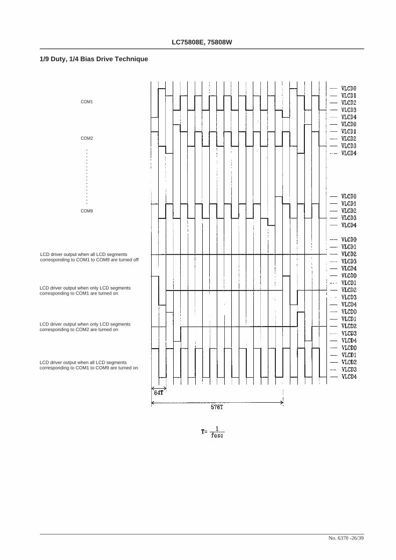
1/8 Duty, 1/4 Bias Drive Technique
LCD driver output when all LCD segmentscorresponding to COM1 to COM8 are turned off
LCD driver output when only LCD segmentscorresponding to COM1 are turned on
LCD driver output when only LCD segmentscorresponding to COM2 are turned on
LCD driver output when all LCD segmentscorresponding to COM1 to COM8 are turned on
COM1
COM2
COM8
.................
No. 6370 -26/39
LC75808E, 75808W
1/9 Duty, 1/4 Bias Drive Technique
LCD driver output when all LCD segmentscorresponding to COM1 to COM9 are turned off
LCD driver output when only LCD segmentscorresponding to COM1 are turned on
LCD driver output when only LCD segmentscorresponding to COM2 are turned on
LCD driver output when all LCD segmentscorresponding to COM1 to COM9 are turned on
COM1
COM2
COM9
.................

No. 6370 -27/39
LC75808E, 75808W
1/10 Duty, 1/4 Bias Drive Technique
LCD driver output when all LCD segmentscorresponding to COM1 to COM10 are turned off
LCD driver output when only LCD segmentscorresponding to COM1 are turned on
LCD driver output when only LCD segmentscorresponding to COM2 are turned on
LCD driver output when all LCD segmentscorresponding to COM1 to COM10 are turned on
COM1
COM2
COM10
.................
No. 6370 -28/39
LC75808E, 75808W
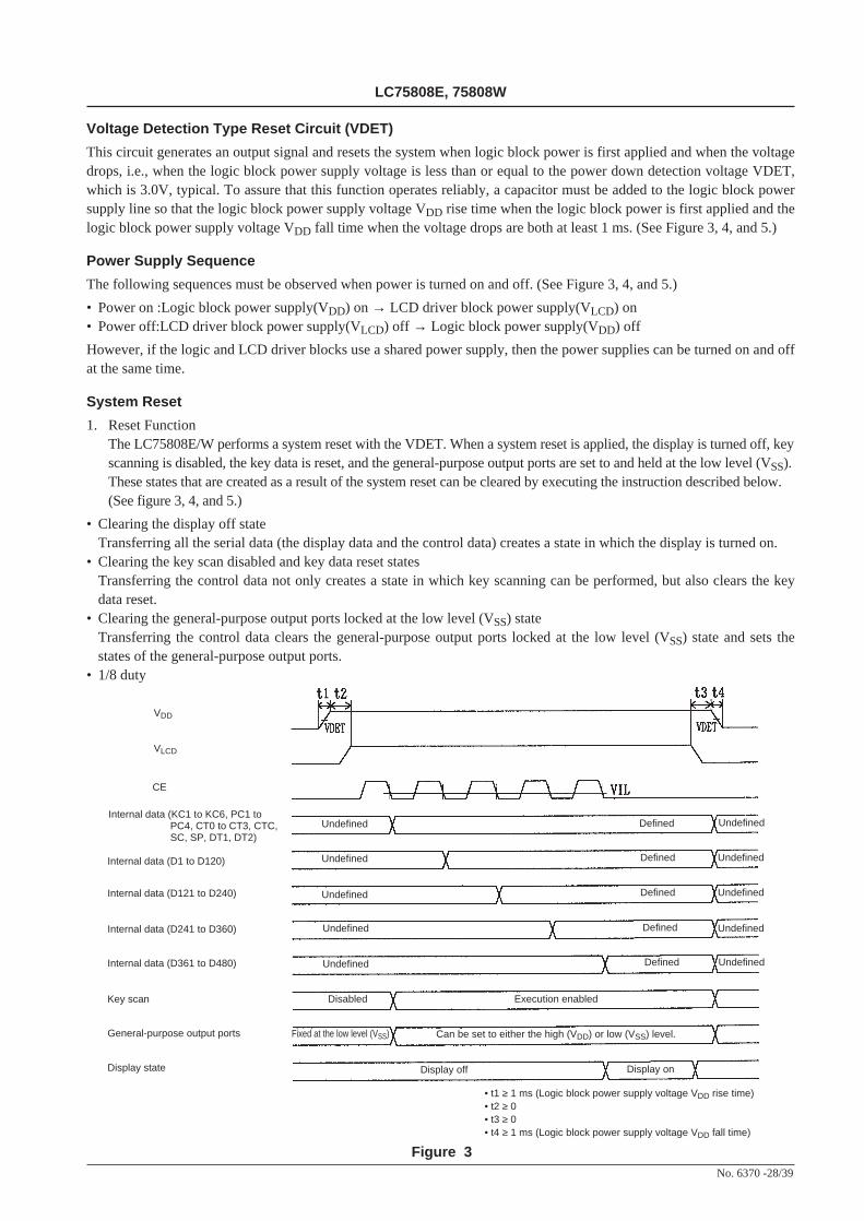
Voltage Detection Type Reset Circuit (VDET)
This circuit generates an output signal and resets the system when logic block power is first applied and when the voltagedrops, i.e., when the logic block power supply voltage is less than or equal to the power down detection voltage VDET,which is 3.0V, typical. To assure that this function operates reliably, a capacitor must be added to the logic block powersupply line so that the logic block power supply voltage VDD rise time when the logic block power is first applied and thelogic block power supply voltage VDD fall time when the voltage drops are both at least 1 ms. (See Figure 3, 4, and 5.)
Power Supply Sequence
The following sequences must be observed when power is turned on and off. (See Figure 3, 4, and 5.)
• Power on :Logic block power supply(VDD) on → LCD driver block power supply(VLCD) on• Power off:LCD driver block power supply(VLCD) off → Logic block power supply(VDD) off
However, if the logic and LCD driver blocks use a shared power supply, then the power supplies can be turned on and offat the same time.
System Reset
1. Reset FunctionThe LC75808E/W performs a system reset with the VDET. When a system reset is applied, the display is turned off, keyscanning is disabled, the key data is reset, and the general-purpose output ports are set to and held at the low level (VSS).These states that are created as a result of the system reset can be cleared by executing the instruction described below.(See figure 3, 4, and 5.)
• Clearing the display off stateTransferring all the serial data (the display data and the control data) creates a state in which the display is turned on.
• Clearing the key scan disabled and key data reset statesTransferring the control data not only creates a state in which key scanning can be performed, but also clears the keydata reset.
• Clearing the general-purpose output ports locked at the low level (VSS) stateTransferring the control data clears the general-purpose output ports locked at the low level (VSS) state and sets thestates of the general-purpose output ports.
• 1/8 duty
• t1 ≥ 1 ms (Logic block power supply voltage VDD rise time)• t2 ≥ 0• t3 ≥ 0• t4 ≥ 1 ms (Logic block power supply voltage VDD fall time)
Internal data (KC1 to KC6, PC1 toPC4, CT0 to CT3, CTC,SC, SP, DT1, DT2)
Internal data (D1 to D120)
Internal data (D121 to D240)
Internal data (D241 to D360)
Internal data (D361 to D480)
Key scan
General-purpose output ports
Display state
Undefined Defined
Figure 3
CE
VLCD
VDD
Undefined
Undefined
Undefined
Undefined
Undefined
Undefined
Undefined
Undefined
Undefined
Disabled
Fixed at the low level (VSS)
Display off
Execution enabled
Can be set to either the high (VDD) or low (VSS) level.
Display on
Defined
Defined
Defined
Defined

• 1/9 duty
No. 6370 -29/39
LC75808E, 75808W
• t1 ≥ 1 ms (Logic block power supply voltage VDD rise time)• t2 ≥ 0• t3 ≥ 0• t4 ≥ 1 ms (Logic block power supply voltage VDD fall time)
Internal data (D1 to D135)
Internal data (D136 to D270)
Internal data (D271 to D405)
Internal data (D406 to D540)
Key scan
General-purpose output ports
Display state
Figure 4
• 1/10 duty
• t1 ≥ 1 ms (Logic block power supply voltage VDD rise time)• t2 ≥ 0• t3 ≥ 0• t4 ≥ 1 ms (Logic block power supply voltage VDD fall time)
Internal data (D1 to D150)
Internal data (D151 to D300)
Internal data (D301 to D450)
Internal data (D451 to D600)
Key scan
General-purpose output ports
Display state
Figure 5
Internal data (KC1 to KC6, PC1 toPC4, CT0 to CT3, CTC,SC, SP, DT1, DT2)
CE
VLCD
VDD
Undefined Defined
Undefined
Undefined
Undefined
Undefined
Undefined
Undefined
Undefined
Undefined
Undefined
Disabled
Fixed at the low level (VSS)
Display off
Execution enabled
Can be set to either the high (VDD) or low (VSS) level.
Display on
Defined
Defined
Defined
Defined

No. 6370 -30/39
LC75808E, 75808W
2. LC75808E/W internal block states during the system reset• CLOCK GENERATOR
Reset is applied and the base clock is stopped. However, the OSC pin state (normal or sleep mode) is determinedafter the SP control data bit is transferred.
• COMMON DRIVER, SEGMENT DRIVER & LATCHReset is applied and the display is turned off. However, display data can be input to the latch circuit in this state.
• CONTRAST ADJUSTERReset is applied and operation of the display contrast adjustment circuit is disabled. After that, once CT0 to CT3and CTC in the control data have been transferred to the IC it will then be possible to set the display contrast.
• KEY SCAN, KEY BUFFERReset is applied, these circuits are forcibly initialized internally, and key scan operation is disabled. Also, the keydata is all set to 0. After that, once KC1 to KC6 in the control data have been transferred to the IC it will then bepossible to perform key scan operations.
• GENERAL PORTReset is applied and the states of the general-purpose output ports are held fixed at the low level (VSS).
• CCB INTERFACE, SHIFT REGISTER, CONTROL REGISTERSince serial data transfer is possible, these circuits are not reset.
Blocks that are reset

No. 6370 -31/39
LC75808E, 75808W
3. Output pin states during the system reset
Note: *5. Since this output pin is an open-drain output, a pull-up resistor of between 1 kΩ and 10 kΩ is required. This pin is held at the high level even if akey data read operation is performed before the KC1 to KC6 control data has been transferred to the IC.
Output pin State during reset
S1 to S60 L (VLCD4)
COM1 to COM10 L (VLCD4)
KS1 to KS6 L (VSS)
P1 to P4 L (VSS)
DO H *5
Sample Application Circuit 11/8 duty, 1/4 bias drive technique (for use with normal panels)
Note: *6. Add a capacitor to the logic block power supply line so that the logic block power supply voltage VDD rise time when power is applied and thelogic block power supply voltage VDD fall time when power drops are both at least 1 ms, as the LC75808E/W is reset by the VDET.
*7. If a variable resistor is not used for display contrast fine adjustment, the VLCD4 pin must be connected to ground.*8. If the function of the INH pin is not used, the INH pin must be connected to the logic block power supply VDD.*9. The DO pin, being an open-drain output, requires a pull-up resistor. Select a resistance (between 1 kΩ to 10 kΩ) appropriate for the capacitance
of the external wiring so that signal waveforms are not degraded.
From the controller
To the controller
To the controllerpower supply
Key matrix (up to 30 keys)
+5 V
+8 V
C ≥ 0.047 µF
LCD panel
*6
*7
*8
*9
Used with the backlightcontroller or other circuit.
general-purpose output ports

No. 6370 -32/39
LC75808E, 75808W
Sample Application Circuit 21/8 duty, 1/4 bias drive technique (for use with large panels)
Note: *6. Add a capacitor to the logic block power supply line so that the logic block power supply voltage VDD rise time when power is applied and thelogic block power supply voltage VDD fall time when power drops are both at least 1 ms, as the LC75808E/W is reset by the VDET.
*7. If a variable resistor is not used for display contrast fine adjustment, the VLCD4 pin must be connected to ground.*8. If the function of the INH pin is not used, the INH pin must be connected to the logic block power supply VDD.*9. The DO pin, being an open-drain output, requires a pull-up resistor. Select a resistance (between 1 kΩ to 10 kΩ) appropriate for the capacitance
of the external wiring so that signal waveforms are not degraded.
From the controller
To the controller
To the controllerpower supply
Key matrix (up to 30 keys)
+5 V
+8 V
C ≥ 0.047 µF10 kΩ ≥ R ≥ 2.2 kΩ
LCD panel
*6
*7
*8
*9
Used with the backlightcontroller or other circuit.
general-purpose output ports

No. 6370 -33/39
LC75808E, 75808W
Sample Application Circuit 31/9 duty, 1/4 bias drive technique (for use with normal panels)
Note: *6. Add a capacitor to the logic block power supply line so that the logic block power supply voltage VDD rise time when power is applied and thelogic block power supply voltage VDD fall time when power drops are both at least 1 ms, as the LC75808E/W is reset by the VDET.
*7. If a variable resistor is not used for display contrast fine adjustment, the VLCD4 pin must be connected to ground.*8. If the function of the INH pin is not used, the INH pin must be connected to the logic block power supply VDD.*9. The DO pin, being an open-drain output, requires a pull-up resistor. Select a resistance (between 1 kΩ to 10 kΩ) appropriate for the capacitance
of the external wiring so that signal waveforms are not degraded.
Used with the backlightcontroller or other circuit.
From the controller
To the controller
To the controllerpower supply
Key matrix (up to 30 keys)
+5 V
+8 V
C ≥ 0.047 µF
LCD panel
*6
*7
*8
*9
general-purpose output ports
No. 6370 -34/39
LC75808E, 75808W
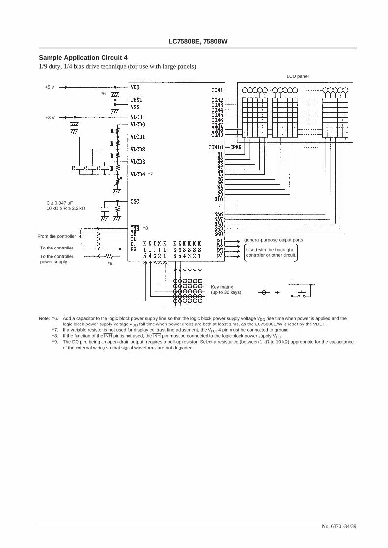
Sample Application Circuit 41/9 duty, 1/4 bias drive technique (for use with large panels)
Note: *6. Add a capacitor to the logic block power supply line so that the logic block power supply voltage VDD rise time when power is applied and thelogic block power supply voltage VDD fall time when power drops are both at least 1 ms, as the LC75808E/W is reset by the VDET.
*7. If a variable resistor is not used for display contrast fine adjustment, the VLCD4 pin must be connected to ground.*8. If the function of the INH pin is not used, the INH pin must be connected to the logic block power supply VDD.*9. The DO pin, being an open-drain output, requires a pull-up resistor. Select a resistance (between 1 kΩ to 10 kΩ) appropriate for the capacitance
of the external wiring so that signal waveforms are not degraded.
From the controller
To the controller
To the controllerpower supply
Key matrix (up to 30 keys)
+5 V
+8 V
C ≥ 0.047 µF10 kΩ ≥ R ≥ 2.2 kΩ
LCD panel
*6
*7
*8
*9
Used with the backlightcontroller or other circuit.
general-purpose output ports

No. 6370 -35/39
LC75808E, 75808W
Sample Application Circuit 51/10 duty, 1/4 bias drive technique (for use with normal panels)
Note: *6. Add a capacitor to the logic block power supply line so that the logic block power supply voltage VDD rise time when power is applied and thelogic block power supply voltage VDD fall time when power drops are both at least 1 ms, as the LC75808E/W is reset by the VDET.
*7. If a variable resistor is not used for display contrast fine adjustment, the VLCD4 pin must be connected to ground.*8. If the function of the INH pin is not used, the INH pin must be connected to the logic block power supply VDD.*9. The DO pin, being an open-drain output, requires a pull-up resistor. Select a resistance (between 1 kΩ to 10 kΩ) appropriate for the capacitance
of the external wiring so that signal waveforms are not degraded.
From the controller
To the controller
To the controllerpower supply
Key matrix (up to 30 keys)
+5 V
+8 V
C ≥ 0.047 µF
LCD panel
*6
*7
*8
*9
Used with the backlightcontroller or other circuit.
general-purpose output ports

No. 6370 -36/39
LC75808E, 75808W
Sample Application Circuit 61/10 duty, 1/4 bias drive technique (for use with large panels)
Note: *6. Add a capacitor to the logic block power supply line so that the logic block power supply voltage VDD rise time when power is applied and thelogic block power supply voltage VDD fall time when power drops are both at least 1 ms, as the LC75808E/W is reset by the VDET.
*7. If a variable resistor is not used for display contrast fine adjustment, the VLCD4 pin must be connected to ground.*8. If the function of the INH pin is not used, the INH pin must be connected to the logic block power supply VDD.*9. The DO pin, being an open-drain output, requires a pull-up resistor. Select a resistance (between 1 kΩ to 10 kΩ) appropriate for the capacitance
of the external wiring so that signal waveforms are not degraded.
Notes on Transferring Display Data from the Controller
The display data is transferred to the LC75808E/W in four operations. All of the display data should be transferred within30 ms to maintain the quality of the displayed image.
From the controller
To the controller
To the controllerpower supply
Key matrix (up to 30 keys)
+5 V
+8 V
C ≥ 0.047 µF10 kΩ ≥ R ≥ 2.2 kΩ
LCD panel
*6
*7
*8
*9
Used with the backlightcontroller or other circuit.
general-purpose output ports

No. 6370 -37/39
LC75808E, 75808W
Notes on the Controller Key Data Read Techniques
1. Timer based key data acquisition
• Flowchart
• Timing chart
t5: Key scan execution time when the key data agreed for two key scans. (800T(s))t6: Key scan execution time when the key data did not agree for two key scans and the key scan was executed again.
(1600T(s))t7: Key address (43H) transfer timet8: Key data read time
• ExplanationIn this technique, the controller uses a timer to determine key on/off states and read the key data. The controller mustcheck the DO state when CE is low every t9 period without fail. If DO is low, the controller recognizes that a key hasbeen pressed and executes the key data read operation.The period t9 in this technique must satisfy the following condition.
t9 > t6 + t7 + t8
If a key data read operation is executed when DO is high, the read key data (KD1 to KD30) and sleep acknowledgedata (SA) will be invalid.
1T = ———fosc
CE = [ L ]
DO = [ L ]

No. 6370 -38/39
LC75808E, 75808W
2. Interrupt based key data acquisition
• Flowchart
• Timing chart
t5: Key scan execution time when the key data agreed for two key scans. (800T(S))t6: Key scan execution time when the key data did not agree for two key scans and the key scan was executed again.
(1600T(S))t7: Key address (43H) transfer timet8: Key data read time
1T = ———fosc
CE = [ L ]
DO = [ L ]
CE = [ L ]
DO = [ H ]

PS No. 6370 -39/39
LC75808E, 75808W
This catalog provides information as of March, 2000. Specifications and information herein are subject tochange without notice.
Specifications of any and all SANYO products described or contained herein stipulate the performance,characteristics, and functions of the described products in the independent state, and are not guaranteesof the performance, characteristics, and functions of the described products as mounted in the customer’sproducts or equipment. To verify symptoms and states that cannot be evaluated in an independent device,the customer should always evaluate and test devices mounted in the customer’s products or equipment.
SANYO Electric Co., Ltd. strives to supply high-quality high-reliability products. However, any and allsemiconductor products fail with some probability. It is possible that these probabilistic failures couldgive rise to accidents or events that could endanger human lives, that could give rise to smoke or fire,or that could cause damage to other property. When designing equipment, adopt safety measures sothat these kinds of accidents or events cannot occur. Such measures include but are not limited to protectivecircuits and error prevention circuits for safe design, redundant design, and structural design.
In the event that any or all SANYO products (including technical data, services) described or containedherein are controlled under any of applicable local export control laws and regulations, such products mustnot be exported without obtaining the export license from the authorities concerned in accordance with theabove law.
No part of this publication may be reproduced or transmitted in any form or by any means, electronic ormechanical, including photocopying and recording, or any information storage or retrieval system,or otherwise, without the prior written permission of SANYO Electric Co., Ltd.
Any and all information described or contained herein are subject to change without notice due toproduct/technology improvement, etc. When designing equipment, refer to the “Delivery Specification”for the SANYO product that you intend to use.
Information (including circuit diagrams and circuit parameters) herein is for example only; it is notguaranteed for volume production. SANYO believes information herein is accurate and reliable, butno guarantees are made or implied regarding its use or any infringements of intellectual property rightsor other rights of third parties.
• ExplanationIn this technique, the controller uses interrupts to determine key on/off states and read the key data. The controller mustcheck the DO state when CE is low. If DO is low, the controller recognizes that a key has been pressed and executesthe key data read operation. After that the next key on/off determination is performed after the time t10 has elapsed bychecking the DO state when CE is low and reading the key data. The period t10 in this technique must satisfy thefollowing condition.
t10 > t6
If a key data read operation is executed when DO is high, the read key data (KD1 to KD30) and sleep acknowledgedata (SA) will be invalid.