
18-Channel Smart Lowside Switch TLE6244X
26
Application Note, V1.0, May 2005 18-Channel Smart Lowside Switch TLE6244X Application Note By Bo Chen Seng-Hung-Tervin Tan Automotive Power Never stop thinking.
Transcript of 18-Channel Smart Lowside Switch TLE6244X

Appl icat ion Note, V1.0, May 2005
18-Channel Smart Lowside Switch TLE6244X
Appl icat ion Note
By Bo ChenSeng-Hung-Tervin Tan
Automot ive Power
N e v e r s t o p t h i n k i n g .
Edition 2004-09Published by Infineon Technologies AG, St.-Martin-Strasse 53, 81669 München, Germany© Infineon Technologies AG 2005. All Rights Reserved.
Attention please!The information herein is given to describe certain components and shall not be considered as a guarantee of characteristics.Terms of delivery and rights to technical change reserved.We hereby disclaim any and all warranties, including but not limited to warranties of non-infringement, regarding circuits, descriptions and charts stated herein.
InformationFor further information on technology, delivery terms and conditions and prices please contact your nearest Infineon Technologies Office (www.infineon.com).
WarningsDue to technical requirements components may contain dangerous substances. For information on the types in question please contact your nearest Infineon Technologies Office.Infineon Technologies Components may only be used in life-support devices or systems with the express written approval of Infineon Technologies, if a failure of such components can reasonably be expected to cause the failure of that life-support device or system, or to affect the safety or effectiveness of that device or system. Life support devices or systems are intended to be implanted in the human body, or to support and/or maintain and sustain and/or protect human life. If they fail, it is reasonable to assume that the health of the user or other persons may be endangered.
Appl icat ion Note, V1.0, May 2005
18-Channel Smart Lowside Switch TLE6244XAppl icat ion NoteVersion 1.0
Automot ive Power
N e v e r s t o p t h i n k i n g .
TLE6244X
Revision History: 2005-5 V1.0 Previous Version: none
V1.0 2005-05
Multi Low-side Switch TLE6244X
Overview
1 OverviewModern Engine Management/Powertrain Systems call for highly integrated intelligent Power Semiconductors under respect of today's and tomorrow's environmental and safety regulations. The growing number of loads must be driven in an intelligent way in combination with real-time fault monitoring. These requirements demand that protection and fault diagnostics be present in the module to meet emission regulations and maintain system reliability.
The TLE6244X is a 18-fold Low-Side Switch in Smart Power Technology (SPT). The device is protected by embedded protection functions, provides Serial Peripheral Interface (SPI) and can be used in PWM applications. It is particularly suitable for applications in engine management and powertrain systems. It has following features:
Features:o Short Circuit Protectiono Over-temperature Protectiono Over-voltage Protectiono 16 bit Serial Data Input and Diagnostic Output (2 bits/Channel. acc. SPI Protocol)o Direct Parallel Control of 16 Channels for PWM Applicationso Low Quiescent Currento Input pins Compatible with 3.3V and 5V Microcontrollerso Electrostatic Discharge (ESD) Protection
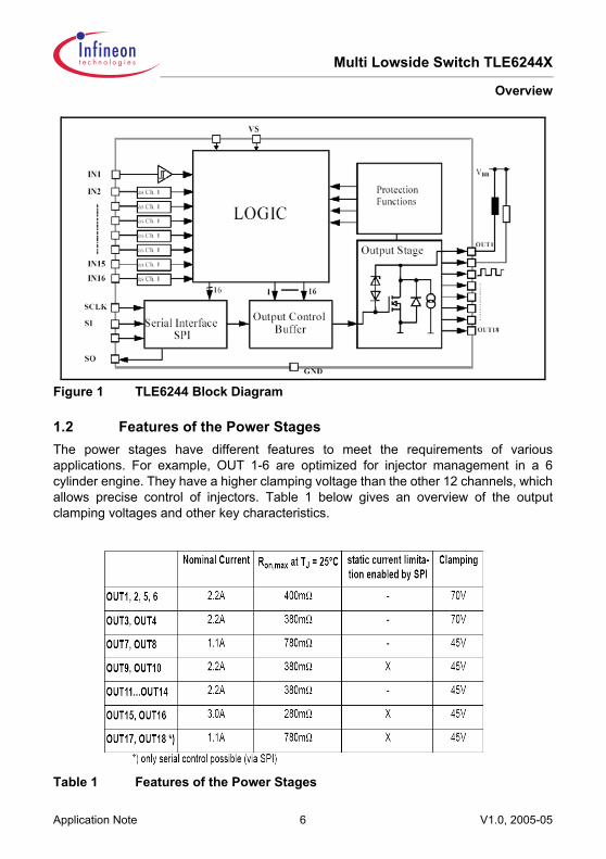
1.1 Detailed Block Diagram TLE6244XThe TLE6244X detailed block diagram is shown in Figure 1. The SPI is present to provide the interface for diagnosis and configuration. All power stages can be controlled by SPI interface. Channel 1-16 have parallel input, which can be used in PWM applications.
Application Note 5 V1.0, 2005-05
Multi Lowside Switch TLE6244X
Overview
Figure 1 TLE6244 Block Diagram
1.2 Features of the Power StagesThe power stages have different features to meet the requirements of various applications. For example, OUT 1-6 are optimized for injector management in a 6 cylinder engine. They have a higher clamping voltage than the other 12 channels, which allows precise control of injectors. Table 1 below gives an overview of the output clamping voltages and other key characteristics.
Table 1 Features of the Power Stages
Application Note 6 V1.0, 2005-05
Multi Low-side Switch TLE6244X
Basic Channel Operation
2 Basic Channel Operation In this section some basic concept and special features of TLE6244X will be introduced in order to facilitate the understanding of the device.
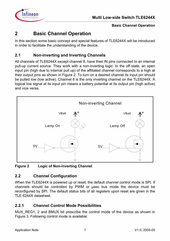
2.1 Non-inverting and Inverting ChannelsAll channels of TLE6244X except channel 8, have their IN pins connected to an internal pull-up current source. They work with a non-inverting logic. In the off state, an open input pin (high due to internal pull up) of the affiliated channel corresponds to a high at their output pins as shown in Figure 2. To turn on a desired channel its input pin should be pulled low (low active). Channel 8 is the only inverting channel on the TLE6244X. A logical low signal at its input pin means a battery potential at its output pin (high active) and vice versa.
VBatt
Lamp On
Non-inverting Channel
VBatt
Lamp Off
0V 5V
Figure 2 Logic of Non-inverting Channel
2.2 Channel ConfigurationWhen the TLE6244X is powered up or reset, the default channel control mode is SPI. If channels should be controlled by PWM or µsec bus mode the device must be reconfigured by SPI. The default status bits of all registers upon reset are given in the TLE 6244X datasheet.
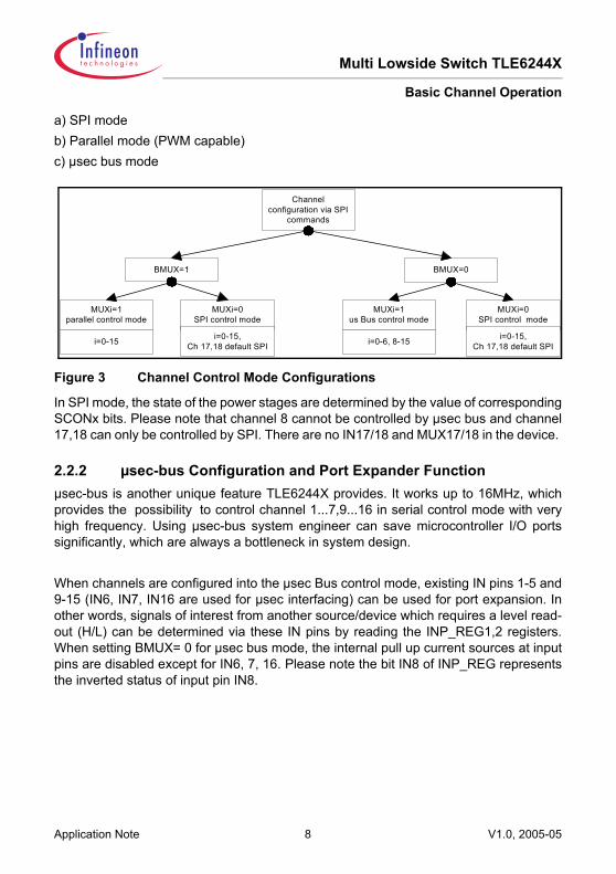
2.2.1 Channel Control Mode Possibilities MUX_REG1, 2 and BMUX bit prescribe the control mode of the device as shown in Figure 3. Following control mode is available:
Application Note 7 V1.0, 2005-05
Multi Lowside Switch TLE6244X
Basic Channel Operation
a) SPI modeb) Parallel mode (PWM capable)c) µsec bus mode
Figure 3 Channel Control Mode Configurations
In SPI mode, the state of the power stages are determined by the value of corresponding SCONx bits. Please note that channel 8 cannot be controlled by µsec bus and channel 17,18 can only be controlled by SPI. There are no IN17/18 and MUX17/18 in the device.
2.2.2 µsec-bus Configuration and Port Expander Functionµsec-bus is another unique feature TLE6244X provides. It works up to 16MHz, which provides the possibility to control channel 1...7,9...16 in serial control mode with very high frequency. Using µsec-bus system engineer can save microcontroller I/O ports significantly, which are always a bottleneck in system design.
When channels are configured into the µsec Bus control mode, existing IN pins 1-5 and 9-15 (IN6, IN7, IN16 are used for µsec interfacing) can be used for port expansion. In other words, signals of interest from another source/device which requires a level read-out (H/L) can be determined via these IN pins by reading the INP_REG1,2 registers. When setting BMUX= 0 for µsec bus mode, the internal pull up current sources at input pins are disabled except for IN6, 7, 16. Please note the bit IN8 of INP_REG represents the inverted status of input pin IN8.
Channelconfiguration via SPI
commands
BMUX=1 BMUX=0
MUXi=1parallel control mode
i=0-15
MUXi=0SPI control mode
i=0-15,Ch 17,18 default SPI
MUXi=1us Bus control mode
i=0-6, 8-15
MUXi=0SPI control mode
i=0-15,Ch 17,18 default SPI
Application Note 8 V1.0, 2005-05
Multi Low-side Switch TLE6244X
Driving Loads
3 Driving Loads
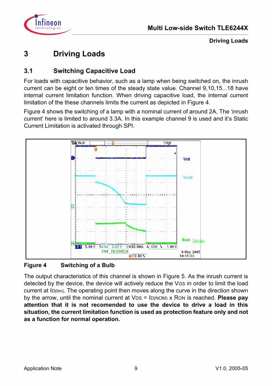
3.1 Switching Capacitive LoadFor loads with capacitive behavior, such as a lamp when being switched on, the inrush current can be eight or ten times of the steady state value. Channel 9,10,15...18 have internal current limitation function. When driving capacitive load, the internal current limitation of the these channels limits the current as depicted in Figure 4.Figure 4 shows the switching of a lamp with a nominal current of around 2A, The ‘inrush current’ here is limited to around 3.3A. In this example channel 9 is used and it’s Static Current Limitation is activated through SPI.
2A/div
Figure 4 Switching of a Bulb
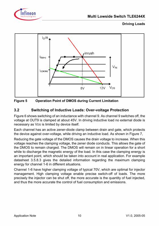
The output characteristics of this channel is shown in Figure 5. As the inrush current is detected by the device, the device will actively reduce the VGS in order to limit the load current at ID(lim). The operating point then moves along the curve in the direction shown by the arrow, until the nominal current at VDS = ID(NOM) x RON is reached. Please pay attention that it is not recomended to use the device to drive a load in this situation, the current limitation function is used as protection feature only and not as a function for normal operation.
Application Note 9 V1.0, 2005-05
Multi Lowside Switch TLE6244X
Driving Loads
Figure 5 Operation Point of DMOS during Current Limitation
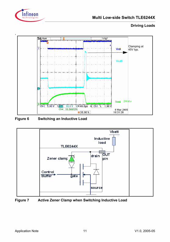
3.2 Switching of Inductive Loads: Over-voltage ProtectionFigure 6 shows switching of an inductance with channel 9. As channel 9 switches off, the voltage at OUT9 is clamped at about 45V. In driving inductive load no external diode is necessary as VDS is limited by device itself.Each channel has an active zener-diode clamp between drain and gate, which protects the device against over-voltage, while driving an inductive load. As shown in Figure 7, Reducing the gate voltage of the DMOS causes the drain voltage to increase. When this voltage reaches the clamping voltage, the zener diode conducts. This allows the gate of the DMOS to remain charged. The DMOS will remain on in linear operation for a short while to discharge the magnetic energy of the load. In this case the clamping energy is an important point, which should be taken into account in real application. For example datasheet 3.5.8.3 gives the detailed information regarding the maximum clamping energy for channel 1-6 in different situations. Channel 1-6 have higher clamping voltage of typical 70V, which are optimal for injector management. High clamping voltage enable precise switch-off of loads. The more precisely the injector can be shut off, the more accurate is the quantity of fuel injected, and thus the more accurate the control of fuel consumption and emissions.
Application Note 10 V1.0, 2005-05
Multi Low-side Switch TLE6244X
Driving Loads
,
:
Clamping at 45V typ.
2A/div2A/div
Figure 6 Switching an Inductive Load
Figure 7 Active Zener Clamp when Switching Inductive Load
Application Note 11 V1.0, 2005-05
Multi Lowside Switch TLE6244X
Fault Detection
4 Fault DetectionEach channel of TLE6244X can distinguish four fault conditions:1) Short-circuit to UBatt (SCB)2) Open Load (OL)3) Short-circuit to Ground (SCG)4) Over Temperature (OT)Each fault is coded into 2 bits, which are stored in the diagnostic registers, DIA_REG1…5. They can be read out by the microcontroller through the SPI interface.
4.1 SPI InterfaceThe serial SPI interface establishes a communication link between TLE6244X and the system microcontroller. All fault information can be read out through SPI. In this section SPI function will be discussed with several examples.
The TLE6244X has a 16-bit SPI. The TLE6244X is selected by the SPI master by an active slave select signal at CS and by the first two bits of the SPI instruction. SI is the data input (Serial In), SO the data output (Serial Out). Via SCK (Serial Clock Input) the SPI clock is provided by the master. The change at output (SO) is forced by the rising edge of the SCK signal. The input signal (SI) is sampled on the falling edge of the SCK signal. The TLE6244X SPI is so called “inter frame response”, which sends the response in the same frame while the normal SPI sends SPI response in the next frame. Furthermore the SPI of TLE6244X is not daisy chain capable, it can not be used in daisy chain application.
The TLE6244X always operates in slave mode whereas the controller provides the master function. A SPI communication starts with a SPI instruction sent from the controller to TLE6244X. During a write cycle the controller sends the data after the SPI instruction, beginning with the MSB. During a reading cycle, after having received the SPI instruction, TLE6244X sends the corresponding data to the controller, also starting with the MSB.
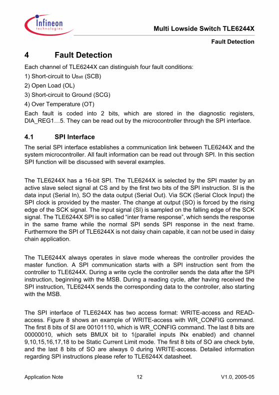
The SPI interface of TLE6244X has two access format: WRITE-access and READ-access. Figure 8 shows an example of WRITE-access with WR_CONFIG command. The first 8 bits of SI are 00101110, which is WR_CONFIG command. The last 8 bits are 00000010, which sets BMUX bit to 1(parallel inputs INx enabled) and channel 9,10,15,16,17,18 to be Static Current Limit mode. The first 8 bits of SO are check byte, and the last 8 bits of SO are always 0 during WRITE-access. Detailed information regarding SPI instructions please refer to TLE6244X datasheet.
Application Note 12 V1.0, 2005-05
Multi Low-side Switch TLE6244X
Fault Detection
Figure 8 SPI Command WR_CONFIG
SI
10 11 01 00
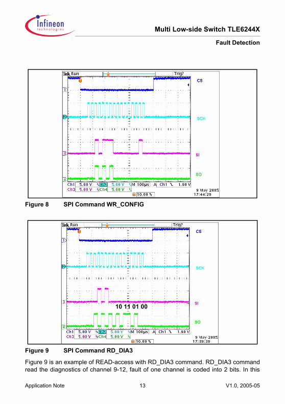
Figure 9 SPI Command RD_DIA3
Figure 9 is an example of READ-access with RD_DIA3 command. RD_DIA3 command read the diagnostics of channel 9-12, fault of one channel is coded into 2 bits. In this
Application Note 13 V1.0, 2005-05
Multi Lowside Switch TLE6244X
Fault Detection
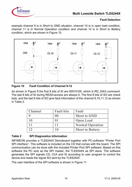
example channel 9 is in Short to GND situation, channel 10 is in open load condition, channel 11 is in Normal Operation condition and channel 12 is in Short to Battery condition, which are shown in Figure 10.
VBatt
Ch9
VBatt
Ch 10
VBatt
Ch 11
VBatt
Ch 12
Figure 10 Fault Condition of Channel 9-12
As shown in Figure 9 the first 8 bits of SI are 00010100, which is RD_DIA3 command. The last 8 bits of SI during READ-access are always 0. The first 8 bits of SO are check byte, and the last 8 bits of SO give fault information of the channel 9,10,11,12 as shown in Table 2.
Channel Fault bits Fault 9 00 Short to GND 10 01 Open Load 11 11 Normal Operation 12 10 Short to Battery
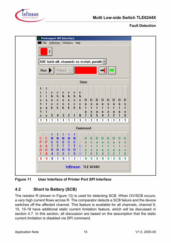
Table 2 SPI Diagnostics InformationINFINEON provides a TLE6244X Demoboard together with PC-software “Printer Port SPI interface”. This software is included on the CD that comes with the board. The SPI communication can be done with the included Printer Port SPI software. Based on this software the PC acts as the SPI master, the TLE6244X as SPI slave. The software generates the SPI signals CS, CLK and SI according to user program to control the device and reads the signal SO sent by the TLE6244X. The user interface of the SPI software is shown in Figure 11
Application Note 14 V1.0, 2005-05
Multi Low-side Switch TLE6244X
Fault Detection
Figure 11 User Interface of Printer Port SPI Interface
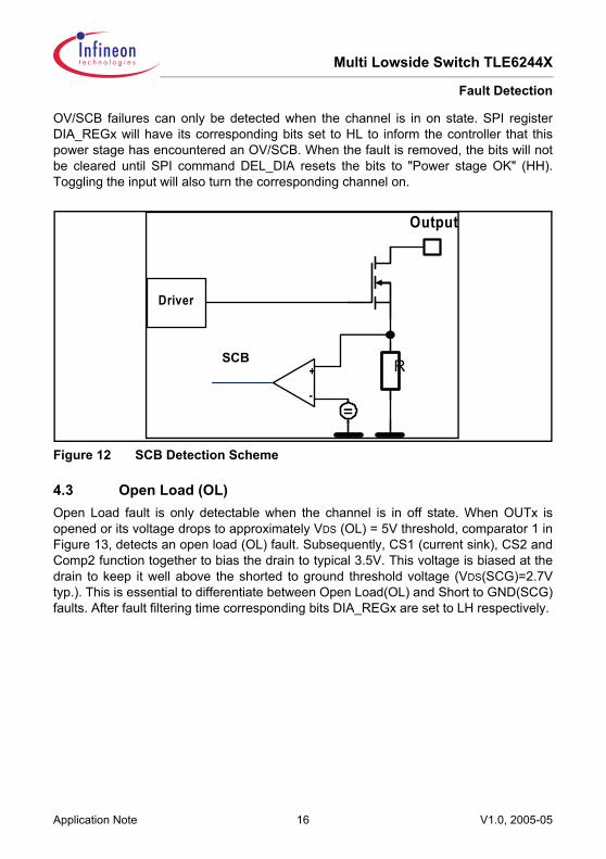
4.2 Short to Battery (SCB)The resistor R (shown in Figure 12) is used for detecting SCB. When OV/SCB occurs, a very high current flows across R. The comparator detects a SCB failure and the device switches off the affected channel. This feature is available for all channels, channel 9, 10, 15-18 have additional static current limitation feature, which will be discussed in section 4.7. In this section, all discussion are based on the assumption that the static current limitation is disabled via SPI command.
Application Note 15 V1.0, 2005-05
Multi Lowside Switch TLE6244X
Fault Detection
OV/SCB failures can only be detected when the channel is in on state. SPI register DIA_REGx will have its corresponding bits set to HL to inform the controller that this power stage has encountered an OV/SCB. When the fault is removed, the bits will not be cleared until SPI command DEL_DIA resets the bits to "Power stage OK" (HH). Toggling the input will also turn the corresponding channel on.
SCB
Output
==
Driver
+
-
R
Figure 12 SCB Detection Scheme
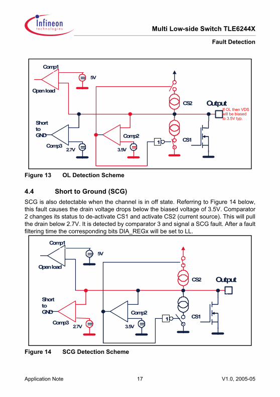
4.3 Open Load (OL)Open Load fault is only detectable when the channel is in off state. When OUTx is opened or its voltage drops to approximately VDS (OL) = 5V threshold, comparator 1 in Figure 13, detects an open load (OL) fault. Subsequently, CS1 (current sink), CS2 and Comp2 function together to bias the drain to typical 3.5V. This voltage is biased at the drain to keep it well above the shorted to ground threshold voltage (VDS(SCG)=2.7V typ.). This is essential to differentiate between Open Load(OL) and Short to GND(SCG) faults. After fault filtering time corresponding bits DIA_REGx are set to LH respectively.
Application Note 16 V1.0, 2005-05
Multi Low-side Switch TLE6244X
Fault Detection
If OL then VDS Output
==3.5V11
==2.7V
==
Comp1
5V
Short to GND
Comp3
Comp2
Open load
CS2
CS1
will be biasedto 3.5V typ.
Figure 13 OL Detection Scheme
4.4 Short to Ground (SCG)SCG is also detectable when the channel is in off state. Referring to Figure 14 below, this fault causes the drain voltage drops below the biased voltage of 3.5V. Comparator 2 changes its status to de-activate CS1 and activate CS2 (current source). This will pull the drain below 2.7V. It is detected by comparator 3 and signal a SCG fault. After a fault filtering time the corresponding bits DIA_REGx will be set to LL.
Output
==3.5V11
==2.7V
==
Comp1
5V
Short to GND
Comp3
Comp2
Open load
CS2
CS1
Figure 14 SCG Detection Scheme
Application Note 17 V1.0, 2005-05
Multi Lowside Switch TLE6244X
Fault Detection
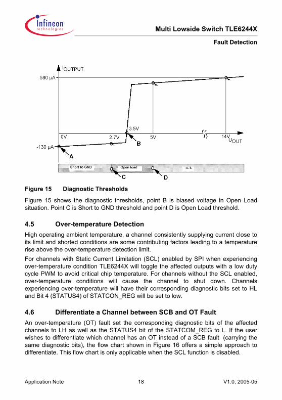
Figure 15 Diagnostic Thresholds
Figure 15 shows the diagnostic thresholds, point B is biased voltage in Open Load situation. Point C is Short to GND threshold and point D is Open Load threshold.
4.5 Over-temperature DetectionHigh operating ambient temperature, a channel consistently supplying current close to its limit and shorted conditions are some contributing factors leading to a temperature rise above the over-temperature detection limit.For channels with Static Current Limitation (SCL) enabled by SPI when experiencing over-temperature condition TLE6244X will toggle the affected outputs with a low duty cycle PWM to avoid critical chip temperature. For channels without the SCL enabled, over-temperature conditions will cause the channel to shut down. Channels experiencing over-temperature will have their corresponding diagnostic bits set to HL and Bit 4 (STATUS4) of STATCON_REG will be set to low.
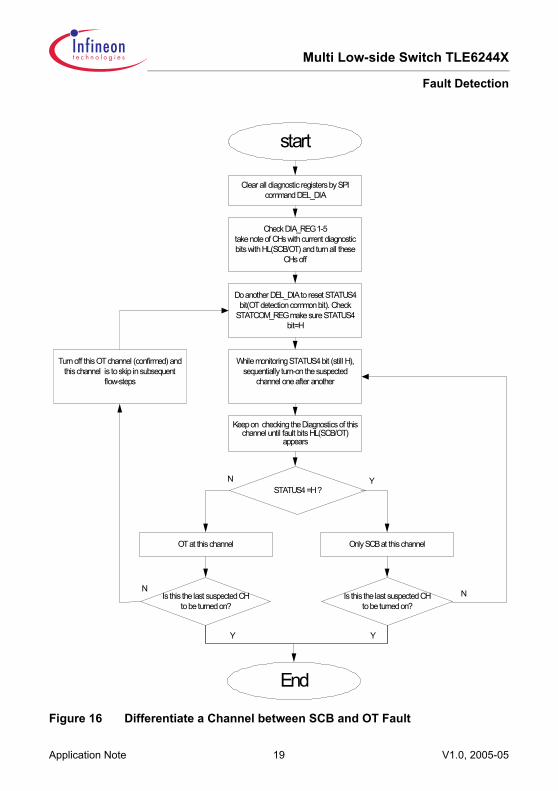
4.6 Differentiate a Channel between SCB and OT Fault An over-temperature (OT) fault set the corresponding diagnostic bits of the affected channels to LH as well as the STATUS4 bit of the STATCOM_REG to L. If the user wishes to differentiate which channel has an OT instead of a SCB fault (carrying the same diagnostic bits), the flow chart shown in Figure 16 offers a simple approach to differentiate. This flow chart is only applicable when the SCL function is disabled.
Application Note 18 V1.0, 2005-05
Multi Low-side Switch TLE6244X
Fault Detection
start
Clear all diagnostic registers by SPIcommand DEL_DIA
Check DIA_REG 1-5take note of CHs with current diagnosticbits with HL(SCB/OT) and turn all these
CHs off
Do another DEL_DIA to reset STATUS4bit(OT detection common bit). Check
STATCOM_REG make sure STATUS4bit=H
While monitoring STATUS4 bit (still H),sequentially turn-on the suspected
channel one after another
STATUS4 =H ?
Only SCB at this channel
Is this the last suspected CHto be turned on?
OT at this channel
Is this the last suspected CHto be turned on?
End
Turn off this OT channel (confirmed) andthis channel is to skip in subsequent
flow-steps
N Y
N
Y
N
Y
Keep on checking the Diagnostics of thischannel until fault bits HL(SCB/OT)
appears
Figure 16 Differentiate a Channel between SCB and OT Fault
Application Note 19 V1.0, 2005-05
Multi Lowside Switch TLE6244X
Fault Detection
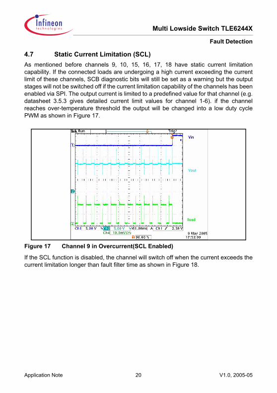
4.7 Static Current Limitation (SCL)As mentioned before channels 9, 10, 15, 16, 17, 18 have static current limitation capability. If the connected loads are undergoing a high current exceeding the current limit of these channels, SCB diagnostic bits will still be set as a warning but the output stages will not be switched off if the current limitation capability of the channels has been enabled via SPI. The output current is limited to a predefined value for that channel (e.g. datasheet 3.5.3 gives detailed current limit values for channel 1-6). if the channel reaches over-temperature threshold the output will be changed into a low duty cycle PWM as shown in Figure 17.
Figure 17 Channel 9 in Overcurrent(SCL Enabled)
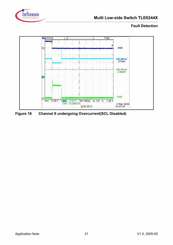
If the SCL function is disabled, the channel will switch off when the current exceeds the current limitation longer than fault filter time as shown in Figure 18.
Application Note 20 V1.0, 2005-05
Multi Low-side Switch TLE6244X
Fault Detection
Figure 18 Channel 9 undergoing Overcurrent(SCL Disabled)
Application Note 21 V1.0, 2005-05
Multi Lowside Switch TLE6244X
VDD Monitoring
5 VDD MonitoringThe VDD monitoring feature provides a device supply-supervision function. This feature ensures that the TLE6244X is adequately supplied within the permissible range of 4.5-5.5V to carry out its operations reliably. If the voltage is not within the permissible range longer than fault filter time, ABE pin would respond by going low, causing all output stages to be turned off. Channel 8 remains on while in parallel mode down to typical VDD=3.5V. This feature guarantee channel 8 functions correctly even in cranking of the engine. A VDD over-voltage (OV) condition will also turn off channel 8. When ABE goes low (valid for VDD over/under voltage condition), STATUS 2 bit of the STATCOM_REG register will go low. To distinguish if there is a over- or an under-voltage condition at VDD, STATUS0 bit goes low for a overvoltage at VDD pin and STATUS1 goes low for a undervoltage at VDD pin. . Here ABE is behaving as a status flag for VDD if VDD goes out of its permissible limits. The ABE pin can be used to disable the other devices on the same system when the VDD goes out of permissible range.
Instead of being used as a status flag, the ABE pin can be used as an additional reset pin. Applying a low voltage to this pin causes all outputs, except OUT8 if it is under parallel control, to be switched off. Thus the host microcontroller can disable the outputs, even though VDD is in its range. Turning the power stages back on using the ABE pin is only possible when VDD remains within its limits.
Application Note 22 V1.0, 2005-05
Multi Low-side Switch TLE6244X
An Example
6 An ExampleAs mensioned before the default control mode of the device is SPI mode, in this section an example is given showing how to set the channel 9 in parallel control mode to drive a capacitive load like a bulb. After power up correctly the following step should be followed:Step 1 Power up the system correctly and note that the ABE and RES pin should be both connected to 5V.
Step 2 Switch off the latch function for overvoltage at VDD with command WR_STATCON, setting CONFIG0(bit5) to 0, shown in Figure 19. This step is optional. Because unexpected Over Voltage fault will be latched and the channel can not be turned on again, this step will make it easier in the first try. In a real application with stable power supply this step is not necessary.
SI
Figure 19 Switching off the Latch Function of Overvoltage at VDD Pin
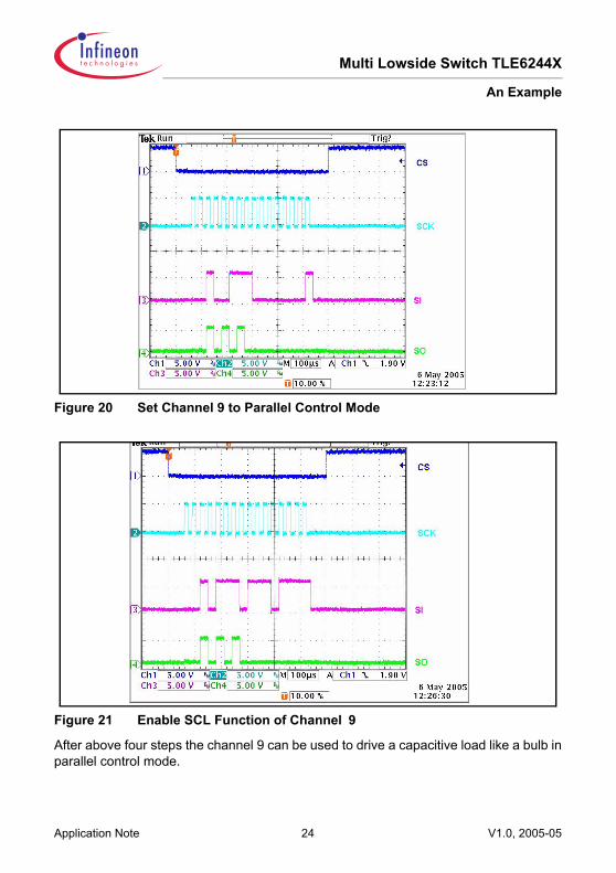
Step 3 Configure channel 9 to parallel control mode with command WR_MUX2, setting the MUX8(bit0) to 1, shown in Figure 20.
Step 4 Enable SCL function of channel 9 with command WR_CONFIG, setting O9-SCB (bit 4) to 0, shown in Figure 21.
Application Note 23 V1.0, 2005-05
Multi Lowside Switch TLE6244X
An Example
Figure 20 Set Channel 9 to Parallel Control Mode
Figure 21 Enable SCL Function of Channel 9
After above four steps the channel 9 can be used to drive a capacitive load like a bulb in parallel control mode.
Application Note 24 V1.0, 2005-05
Multi Low-side Switch TLE6244X
Conclusion
7 ConclusionThe TLE6244X is an integrated 18-channel low-side switch which combines both power and logic in one single chip based on INFINEON Smart Power Technology (SPT). The device features on-chip fault diagnostics for detailed error detection to increase system reliability. 16-bit SPI interface provides a flexible configuration and communication link between the system microcontroller and TLE6244X. All these unique features and flexibility enable wide applications of TLE6244X in automotive systems especially Powertrain/Enginemanegment systems.
Application Note 25 V1.0, 2005-05