16F87X EEPROM Memory Programming Specification...PIC16F87X DS39025E-page 2 2000 Microchip Technology...
22
2000 Microchip Technology Inc. DS39025E-page 1 PIC16F87X This document includes the programming specifications for the following devices: 1.0 PROGRAMMING THE PIC16F87X The PIC16F87X is programmed using a serial method. The serial mode will allow the PIC16F87X to be pro- grammed while in the user’s system. This allows for increased design flexibility. This programming specifi- cation applies to PIC16F87X devices in all packages. 1.1 Programming Algorithm R equirements The programming algorithm used depends on the operating voltage (VDD) of the PIC16F87X device. Algorithm 1 is designed for a VDD range of 2.2V ≤ VDD < 5.5V. Algorithm 2 is for a range of 4.5V ≤ VDD ≤ 5.5V. Either algorithm can be used with the two available programming entry methods. The first method follows the normal Microchip programming mode entry of applying a VPP voltage of 13V ± .5V. The second method, called Low Voltage ICSP TM or LVP for short, applies VDD to MCLR and uses the I/O pin RB3 to enter programming mode. When RB3 is driven to VDD from ground, the PIC16F87X device enters pro- gramming mode. 1.2 Programming Mode The programming mode for the PIC16F87X allows pro- gramming of user program memory, data memory, spe- cial locations used for ID, and the configuration word. Pin Diagram • PIC16F870 • PIC16F874 • PIC16F871 • PIC16F876 • PIC16F872 • PIC16F877 • PIC16F873 PDIP, SOIC RB7 RB6 RB5 RB4 RB3 RB2 RB1 RB0/INT VDD VSS RD7/PSP7 RD6/PSP6 RD5/PSP5 RD4/PSP4 RC7/RX/DT RC6/TX/CK RC5/SDO RC4/SDI/SDA RD3/PSP3 RD2/PSP2 MCLR /VPP RA0/AN0 RA1/AN1 RA2/AN2/VREF RA3/AN3/VREF RA4/T0CKI RA5/AN4/SS RE0/RD /AN5 RE1/WR /AN6 RE2/CS /AN7 VDD VSS OSC1/CLKIN OSC2/CLKOUT RC0/T1OSO/T1CKI RC1/T1OSI/CCP2 RC2/CCP1 RC3/SCK/SCL RD0/PSP0 RD1/PSP1 1 2 3 4 5 6 7 8 9 10 11 12 13 14 15 16 17 18 19 20 40 39 38 37 36 35 34 33 32 31 30 29 28 27 26 25 24 23 22 21 PIC16F877/874/871 PIC16F876/873/872/870 10 11 2 3 4 5 6 1 8 7 9 12 13 14 15 16 17 18 19 20 23 24 25 26 27 28 22 21 MCLR /VPP RA0/AN0 RA1/AN1 RA2/AN2/VREF RA3/AN3/VREF RA4/T0CKI RA5/AN4/SS VSS OSC1/CLKIN OSC2/CLKOUT RC0/T1OSO/T1CKI RC1/T1OSI/CCP2 RC2/CCP1 RC3/SCK/SCL RB7 RB6 RB5 RB4 RB3 RB2 RB1 RB0/INT VDD VSS RC7/RX/DT RC6/TX/CK RC5/SDO RC4/SDI/SDA EEPROM Memory Programming Specification In-circuit Serial Programming (ICSP) is a trademark of Microchip Technology Inc.
Transcript of 16F87X EEPROM Memory Programming Specification...PIC16F87X DS39025E-page 2 2000 Microchip Technology...

2000 Microchip Technology Inc. DS39025E-page 1
PIC16F87X
This document includes the programming specifications for the following devices:
1.0 PROGRAMMING THE PIC16F87X
The PIC16F87X is programmed using a serial method.The serial mode will allow the PIC16F87X to be pro-grammed while in the user’s system. This allows forincreased design flexibility. This programming specifi-cation applies to PIC16F87X devices in all packages.
1.1 Programming Algorithm Requirements
The programming algorithm used depends on theoperating voltage (VDD) of the PIC16F87X device.Algorithm 1 is designed for a VDD range of2.2V ≤ VDD < 5.5V. Algorithm 2 is for a range of4.5V ≤ VDD ≤ 5.5V. Either algorithm can be used withthe two available programming entry methods. The firstmethod follows the normal Microchip programmingmode entry of applying a VPP voltage of 13V ± .5V. Thesecond method, called Low Voltage ICSPTM or LVP forshort, applies VDD to MCLR and uses the I/O pin RB3to enter programming mode. When RB3 is driven toVDD from ground, the PIC16F87X device enters pro-gramming mode.
1.2 Programming Mode
The programming mode for the PIC16F87X allows pro-gramming of user program memory, data memory, spe-cial locations used for ID, and the configuration word.
Pin Diagram
• PIC16F870 • PIC16F874
• PIC16F871 • PIC16F876
• PIC16F872 • PIC16F877
• PIC16F873
PDIP, SOIC
RB7RB6
RB5
RB4RB3
RB2
RB1
RB0/INT
VDD
VSS
RD7/PSP7
RD6/PSP6RD5/PSP5
RD4/PSP4
RC7/RX/DT
RC6/TX/CK
RC5/SDO
RC4/SDI/SDARD3/PSP3
RD2/PSP2
MCLR/VPP
RA0/AN0
RA1/AN1RA2/AN2/VREF
RA3/AN3/VREF
RA4/T0CKI
RA5/AN4/SS
RE0/RD/AN5
RE1/WR/AN6
RE2/CS/AN7VDD
VSS
OSC1/CLKIN
OSC2/CLKOUT
RC0/T1OSO/T1CKI
RC1/T1OSI/CCP2
RC2/CCP1
RC3/SCK/SCLRD0/PSP0
RD1/PSP1
1
2
3
4
5
6
7
8
9
10
11
12
13
14
15
16
17
18
19
20
40
39
38
37
36
35
34
33
32
31
30
2928
27
26
25
24
23
22
21
PIC
16F877/874/871
PIC
16F876/873/872/870
1011
23456
1
87
9
121314 15
1617181920
232425
262728
2221
MCLR/VPP
RA0/AN0RA1/AN1
RA2/AN2/VREF
RA3/AN3/VREF
RA4/T0CKIRA5/AN4/SS
VSS
OSC1/CLKINOSC2/CLKOUT
RC0/T1OSO/T1CKIRC1/T1OSI/CCP2
RC2/CCP1RC3/SCK/SCL
RB7RB6RB5RB4RB3RB2RB1RB0/INTVDD
VSS
RC7/RX/DTRC6/TX/CKRC5/SDORC4/SDI/SDA
EEPROM Memory Programming Specification
In-circuit Serial Programming (ICSP) is a trademark of Microchip Technology Inc.

PIC16F87X
DS39025E-page 2 2000 Microchip Technology Inc.
PIN DESCRIPTIONS (DURING PROGRAMMING): PIC16F87X
Pin NameDuring Programming
Function Pin Type Pin Description
RB3 PGM I Low voltage ICSP programming input if LVPconfiguration bit equals 1
RB6 CLOCK I Clock input
RB7 DATA I/O Data input/output
MCLR VTEST MODE P* Program Mode Select
VDD VDD P Power Supply
VSS VSS P Ground
Legend: I = Input, O = Output, P = Power
*In the PIC16F87X, the programming high voltage is internally generated. To activate the programming mode, high voltage needs tobe applied to MCLR input. Since the MCLR is used for a level source, this means that MCLR does not draw any significant current.

2000 Microchip Technology Inc. DS39025E-page 3
PIC16F87X
2.0 PROGRAM MODE ENTRY
2.1 User Program Memory Map
The user memory space extends from 0x0000 to0x1FFF (8K). In programming mode, the programmemory space extends from 0x0000 to 0x3FFF, withthe first half (0x0000-0x1FFF) being user programmemory and the second half (0x2000-0x3FFF) beingconfiguration memory. The PC will increment from0x0000 to 0x1FFF and wrap to 0x0000, 0x2000 to0x3FFF and wrap around to 0x2000 (not to 0x0000).Once in configuration memory, the highest bit of the PCstays a ‘1’, thus always pointing to the configurationmemory. The only way to point to user program mem-ory is to reset the part and reenter program/verify modeas described in Section 2.4.
In the configuration memory space, 0x2000-0x200Fare physically implemented. However, only locations0x2000 through 0x2007 are available. Other locationsare reserved. Locations beyond 0x200F will physicallyaccess user memory (See Figure 2-1).
2.2 Data EEPROM Memory
The EEPROM data memory space is a separate blockof high endurance memory that the user accessesusing a special sequence of instructions. The amountof data EEPROM memory depends on the device andis shown below in number of bytes.
The contents of data EEPROM memory have the capa-bility to be embedded into the hex file.
The programmer should be able to read data EEPROMinformation from a hex file and conversely (as anoption), write data EEPROM contents to a hex filealong with program memory information and configura-tion bit information.
The 256 data memory locations are logically mappedstarting at address 0x2100. The format for data mem-ory storage is one data byte per address location, LSBaligned.
Device # of Bytes
PIC16F870 64
PIC16F871 64
PIC16F872 64
PIC16F873 128
PIC16F874 128
PIC16F876 256
PIC16F877 256

PIC16F87X
DS39025E-page 4 2000 Microchip Technology Inc.
2.3 ID Locations
A user may store identification information (ID) in fourID locations. The ID locations are mapped in [0x2000 :0x2003]. It is recommended that the user use only thefour least significant bits of each ID location. In somedevices, the ID locations read-out in an unscrambledfashion after code protection is enabled. For thesedevices, it is recommended that ID location is written as“11 1111 1000 bbbb” where ‘bbbb’ is ID information.
In other devices, the ID locations read out normally,even after code protection. To understand how thedevices behave, refer to Table 5-1.
To understand the scrambling mechanism after codeprotection, refer to Section 4.0.
FIGURE 2-1: PROGRAM MEMORY MAPPING
2Kwords
4Kwords
8Kwords
Implemented Implemented Implemented
Implemented Implemented Implemented
Implemented Implemented
Implemented Implemented
Reserved Implemented
Reserved Implemented
Implemented
Implemented
Reserved Reserved Reserved
Reserved Reserved Reserved
ID Location
ID Location
ID Location
ID Location
Reserved
Reserved
Device ID
Configuration Word
2000h
2001h
2002h
2003h
2004h
2005h
2006h
2007h
0h
1FFh
3FFh
400h
7FFh
800h
BFFh
C00h
FFFh
1000h
1FFFh
2008h
2100h
3FFFh

2000 Microchip Technology Inc. DS39025E-page 5
PIC16F87X
2.4 Program/Verify Mode
The program/verify mode is entered by holding pinsRB6 and RB7 low while raising MCLR pin from VIL toVIHH (high voltage). In this mode, the state of the RB3pin does not effect programming. Low voltage ICSPprogramming mode is entered by raising RB3 from VIL
to VDD and then applying VDD to MCLR. Once in thismode, the user program memory and the configurationmemory can be accessed and programmed in serialfashion. The mode of operation is serial, and the mem-ory that is accessed is the user program memory. RB6and RB7 are Schmitt Trigger Inputs in this mode.
The sequence that enters the device into the program-ming/verify mode places all other logic into the RESETstate (the MCLR pin was initially at VIL). This meansthat all I/O are in the RESET state (high impedanceinputs).
The normal sequence for programming is to use theload data command to set a value to be written at theselected address. Issue the begin programming com-mand followed by read data command to verify, andthen increment the address.
A device RESET will clear the PC and set the addressto 0. The “increment address” command will incrementthe PC. The “load configuration” command will set thePC to 0x2000. The available commands are shown inTable 2-1.
2.4.1 LOW VOLTAGE ICSP PROGRAMMING MODE
Low voltage ICSP programming mode allows aPIC16F87X device to be programmed using VDD only.However, when this mode is enabled by a configurationbit (LVP), the PIC16F87X device dedicates RB3 to con-trol entry/exit into programming mode.
When LVP bit is set to ‘1’, the low voltage ICSP pro-gramming entry is enabled. Since the LVP configura-tion bit allows low voltage ICSP programming entry inits erased state, an erased device will have the LVP bitenabled at the factory. While LVP is ‘1’, RB3 is dedi-cated to low voltage ICSP programming. Bring RB3 toVDD and then MCLR to VDD to enter programmingmode. All other specifications for high voltage ICSP™apply.
To disable low voltage ICSP mode, the LVP bit must beprogrammed to ‘0’. This must be done while enteredwith high voltage entry mode (LVP bit = 1). RB3 is nowa general purpose I/O pin.
2.4.2 SERIAL PROGRAM/VERIFY OPERATION
The RB6 pin is used as a clock input pin, and the RB7pin is used for entering command bits and data input/output during serial operation. To input a command, theclock pin (RB6) is cycled six times. Each command bitis latched on the falling edge of the clock with the leastsignificant bit (LSb) of the command being input first.The data on pin RB7 is required to have a minimumsetup and hold time (see AC/DC specifications), withrespect to the falling edge of the clock. Commands thathave data associated with them (read and load) arespecified to have a minimum delay of 1 µs between thecommand and the data. After this delay, the clock pin iscycled 16 times with the first cycle being a Start bit andthe last cycle being a Stop bit. Data is also input andoutput LSb first.
Therefore, during a read operation the LSb will betransmitted onto pin RB7 on the rising edge of the sec-ond cycle, and during a load operation the LSb will belatched on the falling edge of the second cycle. A min-imum 1µs delay is also specified between consecutivecommands.
All commands are transmitted LSb first. Data wordsare also transmitted LSb first. The data is transmittedon the rising edge and latched on the falling edge ofthe clock. To allow for decoding of commands andreversal of data pin configuration, a time separation ofat least 1 µs is required between a command and adata word (or another command).
The commands that are available are:
2.4.2.1 LOAD CONFIGURATION
After receiving this command, the program counter(PC) will be set to 0x2000. By then applying 16 cyclesto the clock pin, the chip will load 14-bits in a “dataword,” as described above, to be programmed into theconfiguration memory. A description of the memorymapping schemes of the program memory for normaloperation and configuration mode operation is shownin Figure 2-1. After the configuration memory isentered, the only way to get back to the user programmemory is to exit the program/verify test mode by tak-ing MCLR low (VIL).
2.4.2.2 LOAD DATA FOR PROGRAM MEMORY
After receiving this command, the chip will load in a14-bit “data word” when 16 cycles are applied, asdescribed previously. A timing diagram for the loaddata command is shown in Figure 6-1.
Note: The OSC must not have 72 osc clockswhile the device MCLR is between VIL andVIHH.

PIC16F87X
DS39025E-page 6 2000 Microchip Technology Inc.
2.4.2.3 LOAD DATA FOR DATA MEMORY
After receiving this command, the chip will load in a14-bit “data word” when 16 cycles are applied. How-ever, the data memory is only 8-bits wide, and thus onlythe first 8-bits of data after the Start bit will be pro-grammed into the data memory. It is still necessary tocycle the clock the full 16 cycles in order to allow theinternal circuitry to reset properly. The data memorycontains up to 256 bytes. If the device is code pro-tected, the data is read as all zeros.
2.4.2.4 READ DATA FROM PROGRAM MEMORY
After receiving this command, the chip will transmitdata bits out of the program memory (user or configu-ration) currently accessed, starting with the second ris-ing edge of the clock input. The RB7 pin will go intooutput mode on the second rising clock edge, and it willrevert back to input mode (hi-impedance) after the 16thrising edge. A timing diagram of this command isshown in Figure 6-2.
2.4.2.5 READ DATA FROM DATA MEMORY
After receiving this command, the chip will transmitdata bits out of the data memory starting with the sec-ond rising edge of the clock input. The RB7 pin will gointo output mode on the second rising edge, and it willrevert back to input mode (hi-impedance) after the 16thrising edge. As previously stated, the data memory is 8-bits wide, and therefore, only the first 8-bits that areoutput are actual data.
2.4.2.6 INCREMENT ADDRESS
The PC is incremented when this command isreceived. A timing diagram of this command is shownin Figure 6-3.
2.4.2.7 BEGIN ERASE/PROGRAM CYCLE
A load command must be given before every beginprogramming command. Programming of the appro-priate memory (test program memory, user programmemory or data memory) will begin after this commandis received and decoded. An internal timing mechanismexecutes an erase before write. The user must allow forboth erase and programming cycle times for program-ming to complete. No “end programming” command isrequired.
2.4.2.8 BEGIN PROGRAMMING
A load command must be given before every beginprogramming command. Programming of the appro-priate memory (test program memory, user programmemory or data memory) will begin after this commandis received and decoded. An internal timing mechanismexecutes a write. The user must allow for programcycle time for programming to complete. No “end pro-gramming” command is required.
This command is similar to the ERASE/PROGRAMCYCLE command, except that a word erase is notdone. It is recommended that a bulk erase be per-formed before starting a series of programming onlycycles.
Note: The Begin Program operation must takeplace at 4.5 to 5.5 VDD range.
TABLE 2-1: COMMAND MAPPING FOR PIC16F87X
Command Mapping (MSB … LSB) DataVoltage Range
Load Configuration X X 0 0 0 0 0, data (14), 0 2.2V - 5.5V
Load Data for Program Memory X X 0 0 1 0 0, data (14), 0 2.2V - 5.5V
Read Data from Program Memory X X 0 1 0 0 0, data (14), 0 2.2V - 5.5V
Increment Address X X 0 1 1 0 2.2V - 5.5V
Begin Erase Programming Cycle 0 0 1 0 0 0 2.2V - 5.5V
Begin Programming Only Cycle 0 1 1 0 0 0 4.5V - 5.5V
Load Data for Data Memory X X 0 0 1 1 0, data (14), 0 2.2V - 5.5V
Read Data from Data Memory X X 0 1 0 1 0, data (14), 0 2.2V - 5.5V
Bulk Erase Setup1 0 0 0 0 0 1 4.5V - 5.5V
Bulk Erase Setup2 0 0 0 1 1 1 4.5V - 5.5V

2000 Microchip Technology Inc. DS39025E-page 7
PIC16F87X
2.5 Erasing Program and Data Memory
Depending on the state of the code protection bits, pro-gram and data memory will be erased using differentprocedures. The first set of procedures is used whenboth program and data memories are not code pro-tected. The second set of procedures must be usedwhen either memory is code protected. A device pro-grammer should determine the state of the code pro-tection bits and then apply the proper procedure toerase the desired memory.
2.5.1 ERASING NON-CODE PROTECTED PROGRAM AND DATA MEMORY
When both program and data memories are not codeprotected, they must be individually erased using thefollowing procedures. The only way that both memoriesare erased using a single procedure is if code protec-tion is enabled for one of the memories. These proce-dures do not erase the configuration word or IDlocations.
Procedure to bulk erase program memory:
1. Execute a Load Data for Program Memory com-mand (000010) with a ’1’ in all locations(0x3FFF)
2. Execute a Bulk Erase Setup1 command(000001)
3. Execute a Bulk Erase Setup2 command(000111)
4. Execute a Begin Erase/Programming command(001000)
5. Wait 8ms
6. Execute a Bulk Erase Setup1 command(000001)
7. Execute a Bulk Erase Setup2 command(000111)
Procedure to bulk erase data memory:
1. Execute a Load Data for Data Memory com-mand (000011) with a ’1’ in all locations(0x3FFF)
2. Execute a Bulk Erase Setup1 command(000001)
3. Execute a Bulk Erase Setup2 command(000111)
4. Execute a Begin Erase/Programming command(001000)
5. Wait 8ms6. Execute a Bulk Erase Setup1 command
(000001)7. Execute a Bulk Erase Setup2 command
(000111)
2.5.2 ERASING CODE PROTECTED MEMORY
For the PIC16F87X devices, once code protection isenabled, all protected program and data memory loca-tions read all ’0’s and further programming is disabled.The ID locations and configuration word read outunscrambled and can be reprogrammed normally. Theonly procedure to erase a PIC16F87X device that iscode protected is shown in the following procedure.This method erases program memory, data memory,configuration bits and ID locations. Since all datawithin the program and data memory will be erasedwhen this procedure is executed, the security ofthe data or code is not compromised.
1. Execute a Load Configuration command(000000) with a ’1’ in all locations (0x3FFF)
2. Execute Increment Address command(000110) to set address to configuration wordlocation (0x2007)
3. Execute a Bulk Erase Setup1 command(000001)
4. Execute a Bulk Erase Setup2 command(000111)
5. Execute a Begin Erase/Programming command(001000)
6. Wait 8ms7. Execute a Bulk Erase Setup1 command
(000001)8. Execute a Bulk Erase Setup2 command
(000111)

PIC16F87X
DS39025E-page 8 2000 Microchip Technology Inc.
FIGURE 2-2: PROGRAM FLOW CHART - PIC16F87X PROGRAM MEMORY (2.2V ≤ VDD < 5.5V)
Start
Set VDD = VDDP
Load Data
Wait tprog
All LocationsDone?
Verify allLocations
Data Correct?
Done
IncrementAddress
Command
Report VerifyError
No
No
Command
BeginErase/Programming
Command

2000 Microchip Technology Inc. DS39025E-page 9
PIC16F87X
FIGURE 2-3: PROGRAM FLOW CHART - PIC16F87X PROGRAM MEMORY (4.5V ≤ VDD ≤ 5.5V)
Start
Set VDD = VDDP
Load Data
Wait tprog
All LocationsDone?
Done
IncrementAddress
Command
No
Command
BeginProgramming Only
Command
Bulk EraseSequence
Verify all
Data Correct?
Locations
IncrementAddress
Command
NoReport VerifyError
PIC16F87X
DS39025E-page 10 2000 Microchip Technology Inc.
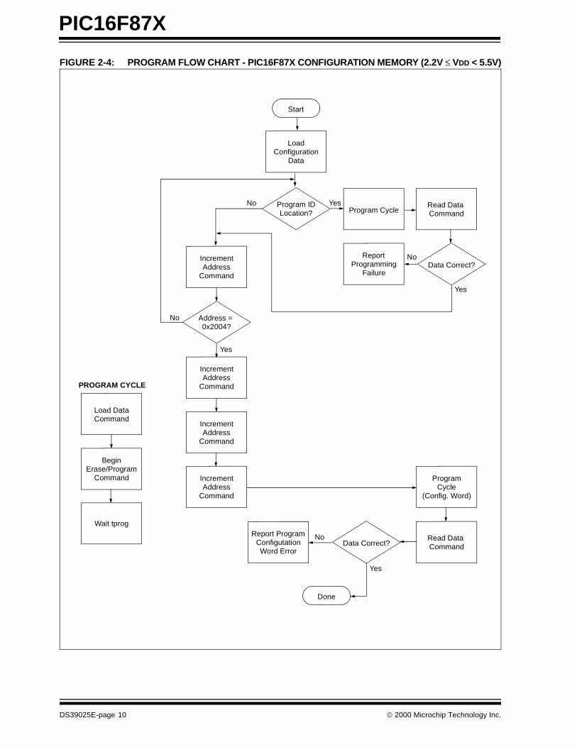
FIGURE 2-4: PROGRAM FLOW CHART - PIC16F87X CONFIGURATION MEMORY (2.2V ≤ VDD < 5.5V)
Program ID
Start
LoadConfiguration
Data
Location? Program CycleRead Data Command
Data Correct?Report
ProgrammingFailure
IncrementAddress
Command
IncrementAddress
Command
IncrementAddress
Command
IncrementAddress
Command
ProgramCycle
(Config. Word)
Read Data CommandData Correct?
Report ProgramConfigutationWord Error
Done
Yes
No
YesNo
No
Yes
Yes
No
Load DataCommand
BeginErase/Program
Command
Wait tprog
Address = 0x2004?
PROGRAM CYCLE

2000 Microchip Technology Inc. DS39025E-page 11
PIC16F87X
FIGURE 2-5: PROGRAM FLOW CHART - PIC16F87X CONFIGURATION MEMORY
Program ID
Start
LoadConfiguration
Data
Location? Program CycleRead Data Command
Data Correct?Report
ProgrammingFailure
IncrementAddress
Command
IncrementAddress
Command
IncrementAddress
Command
IncrementAddress
Command
ProgramCycle
(Config. Word)
Read Data CommandData Correct?
Report ProgramConfigutationWord Error
Done
Yes
No
YesNo
No
Yes
Yes
No
Load DataCommand
BeginProgram Only
Command*
Wait tprog
Address = 0x2004?
PROGRAM CYCLE
*Assumes that a bulk erase was issued before programming configuration word. If not, use the program flow from Figure 2-4.

PIC16F87X
DS39025E-page 12 2000 Microchip Technology Inc.
3.0 CONFIGURATION WORDThe PIC16F87X has several configuration bits. Thesebits can be set (reads ‘0’), or left unchanged (reads ‘1’),to select various device configurations.
3.1 Device ID Word
The device ID word for the PIC16F87X is located at2006h.
TABLE 3-1: DEVICE ID VALUE
DeviceDevice ID Value
Dev Rev
PIC16F870 00 1101 000 x xxxx
PIC16F871 00 1101 001 x xxxx
PIC16F872 00 1000 111 x xxxx
PIC16F873 00 1001 011 x xxxx
PIC16F874 00 1001 001 x xxxx
PIC16F876 00 1001 111 x xxxx
PIC16F877 00 1001 101 x xxxx

2000 Microchip Technology Inc. DS39025E-page 13
PIC16F87X
FIGURE 3-1: CONFIGURATION WORD FOR PIC16F873/874/876/877
CP1 CP0 RESV - WRT CPD LVP BODEN CP1 CP0 PWRTE WDTE F0SC1 F0SC0 Register: CONFIGAddress 2007hbit13 bit0
bit 13-12:bit 11: Reserved: Set to ‘1’ for normal operationbit 5-4: CP1:CP0: FLASH Program Memory Code Protection bits (2)
4K Devices:11 = Code protection off10 = 0F00h to 0FFFh code protected01 = 0800h to 0FFFh code protected00 = 0000h to 0FFFh code protected
8K Devices:11 = Code protection off10 = 1F00h to 1FFFh code protected 01 = 1000h to 1FFFh code protected 00 = 0000h to 1FFFh code protected
bit 11: Reserved: Set to ‘1’ for normal operation bit 10: Unimplemented: Read as ‘1’bit 9: WRT: FLASH Program Memory Write Enable 1 = Unprotected program memory may be written to by EECON control
0 = Unprotected program memory may not be written to by EECON controlbit 8: CPD: Data EE Memory Code Protection 1 = Code protection off
0 = Data EE memory code protected
bit 7: LVP: Low Voltage ICSP Programming Enable bit1 = RB3/PGM pin has PGM function, low voltage programming enabled0 = RB3 is digital I/O, HV on MCLR must be used for programming
bit 6: BODEN: Brown-out Reset Enable bit (1)
1 = BOR enabled0 = BOR disabled
bit 3: PWRTE: Power-up Timer Enable bit (1)
1 = PWRT disabled0 = PWRT enabled
bit 2: WDTE: Watchdog Timer Enable bit1 = WDT enabled0 = WDT disabled
bit 1-0: FOSC1:FOSC0: Oscillator Selection bits11 = RC oscillator10 = HS oscillator01 = XT oscillator00 = LP oscillator
Note 1: Enabling Brown-out Reset automatically enables Power-up Timer (PWRT) regardless of the value of bit PWRTE. Ensure the Power-up Timer is enabled any time Brown-out Reset is enabled.
2: All of the CP1:CP0 pairs have to be given the same value to enable the code protection scheme listed.

PIC16F87X
DS39025E-page 14 2000 Microchip Technology Inc.
FIGURE 3-2: CONFIGURATION WORD FOR PIC16F870/871/872
CP1 CP0 RESV - WRT CPD LVP BODEN CP1 CP0 PWRTE WDTE F0SC1 F0SC0 Register: CONFIGAddress 2007hbit13 bit0
bit 13-12:bit 5-4: CP1:CP0: FLASH Program Memory Code Protection bits (2)
11 = Code protection off10 = not supported01 = not supported00 = 0000h to 07FFh code protected
bit 11: Reserved: Set to ‘1’ for normal operation bit 10: Unimplemented: Read as ‘1’bit 9: WRT: FLASH Program Memory Write Enable 1 = Unprotected program memory may be written to by EECON control
0 = Unprotected program memory may not be written to by EECON controlbit 8: CPD: Data EE Memory Code Protection 1 = Code protection off
0 = Data EE memory code protected
bit 7: LVP: Low Voltage ICSP Programming Enable bit1 = RB3/PGM pin has PGM function, low voltage programming enabled0 = RB3 is digital I/O, HV on MCLR must be used for programming
bit 6: BODEN: Brown-out Reset Enable bit (1)
1 = BOR enabled0 = BOR disabled
bit 3: PWRTE: Power-up Timer Enable bit (1)
1 = PWRT disabled0 = PWRT enabled
bit 2: WDTE: Watchdog Timer Enable bit1 = WDT enabled0 = WDT disabled
bit 1-0: FOSC1:FOSC0: Oscillator Selection bits11 = RC oscillator10 = HS oscillator01 = XT oscillator00 = LP oscillator
Note 1: Enabling Brown-out Reset automatically enables Power-up Timer (PWRT) regardless of the value of bit PWRTE. Ensure the Power-up Timer is enabled any time Brown-out Reset is enabled.
2: All of the CP1:CP0 pairs have to be given the same value to enable the code protection scheme listed.

2000 Microchip Technology Inc. DS39025E-page 15
PIC16F87X
4.0 EMBEDDING CONFIGURATION WORD AND ID INFORMATION IN THE HEX FILE
To allow portability of code, the programmer is required to read the configuration word and ID locations from the hexfile when loading the hex file. If configuration word information was not present in the hex file, then a simple warningmessage may be issued. Similarly, while saving a hex file, configuration word and ID information must be included.An option to not include this information may be provided.
Specifically for the PIC16F87X, the EEPROM data memory should also be embedded in the hex file (seeSection 2.2).
Microchip Technology Inc. feels strongly that this feature is important for the benefit of the end customer.

PIC16F87X
DS39025E-page 16 2000 Microchip Technology Inc.
5.0 CHECKSUM COMPUTATIONChecksum is calculated by reading the contents of thePIC16F87X memory locations and adding up theopcodes up to the maximum user addressable location,e.g., 0x1FF for the PIC16F87X. Any carry bits exceed-ing 16-bits are neglected. Finally, the configurationword (appropriately masked) is added to the check-sum. Checksum computation for each member of thePIC16F87X devices is shown in Table 5-1.
The checksum is calculated by summing the following:
• The contents of all program memory locations• The configuration word, appropriately masked• Masked ID locations (when applicable)
The least significant 16 bits of this sum is the check-sum.
The following table describes how to calculate thechecksum for each device. Note that the checksum cal-culation differs depending on the code protect setting.Since the program memory locations read out differ-ently depending on the code protect setting, the tabledescribes how to manipulate the actual program mem-ory values to simulate the values that would be readfrom a protected device. When calculating a checksumby reading a device, the entire program memory cansimply be read and summed. The configuration wordand ID locations can always be read.
Note that some older devices have an additional valueadded in the checksum. This is to maintain compatibil-ity with older device programmer checksums.

2000 Microchip Technology Inc. DS39025E-page 17
PIC16F87X
TABLE 5-1: CHECKSUM COMPUTATION
DeviceCode
ProtectChecksum*
Blank Value
0x25E6 at 0and maxaddress
PIC16F870 OFF SUM[0x0000:0x07FFF] + CFGW & 0x3BFF 0x33FF 0xFFCD
ALL CFGW & 0x3BFF + SUM_ID 0x3FCE 0x0B9C
PIC16F871 OFF SUM[0x0000:0x07FFF] + CFGW & 0x3BFF 0x33FF 0xFFCD
ALL CFGW & 0x3BFF + SUM_ID 0x3FCE 0x0B9C
PIC16F872 OFF SUM[0x0000:0x07FFF] + CFGW & 0x3BFF 0x33FF 0xFFCD
ALL CFGW & 0x3BFF + SUM_ID 0x3FCE 0x0B9C
PIC16F873 OFF SUM[0x0000:0x0FFF] + CFGW & 0x3BFF 0x2BFF 0xF7CD
0x0F00 : 0xFFF SUM[0x0000:0x0EFF] + CFGW & 0x3BFF +SUM_ID 0x48EE 0xFAA3
0x0800 : 0xFFF SUM[0x0000:0x07FF] + CFGW & 0x3BFF + SUM_ID 0x3FDE 0xF193
ALL CFGW & 0x3BFF + SUM_ID 0x37CE 0x039C
PIC16F874 OFF SUM[0x0000:0x0FFF] + CFGW & 0x3BFF 0x2BFF 0xF7CD
0x0F00 : 0xFFF SUM[0x0000:0x0EFF] + CFGW & 0x3BFF +SUM_ID 0x48EE 0xFAA3
0x0800 : 0xFFF SUM[0x0000:0x07FF] + CFGW & 0x3BFF + SUM_ID 0x3FDE 0xF193
ALL CFGW & 0x3BFF + SUM_ID 0x37CE 0x039C
PIC16F876 OFF SUM[0x0000:0x1FFF] + CFGW & 0x3BFF 0x1BFF 0xE7CD
0x1F00 : 0x1FFF SUM[0x0000:0x1EFF] + CFGW & 0x3BFF +SUM_ID 0x28EE 0xDAA3
0x1000 : 0x1FFF SUM[0x0000:0x0FFF] + CFGW & 0x3BFF + SUM_ID 0x27DE 0xD993
ALL CFGW & 0x3BFF + SUM_ID 0x27CE 0xF39C
PIC16F877 OFF SUM[0x0000:0x1FFF] + CFGW & 0x3BFF 0x1BFF 0xE7CD
0x1F00 : 0x1FFF SUM[0x0000:0x1EFF] + CFGW & 0x3BFF +SUM_ID 0x28EE 0xDAA3
0x1000 : 0x1FFF SUM[0x0000:0x0FFF] + CFGW & 0x3BFF + SUM_ID 0x27DE 0xD993
ALL CFGW & 0x3BFF + SUM_ID 0x27CE 0xF39C
Legend: CFGW = Configuration WordSUM[a:b] = [Sum of locations a to b inclusive]SUM_ID = ID locations masked by 0xF then made into a 16-bit value with ID0 as the most significant nibble. For example, ID0 = 0x1, ID1 = 0x2, ID3 = 0x3, ID4 = 0x4, then SUM_ID = 0x1234*Checksum = [Sum of all the individual expressions] MODULO [0xFFFF]+ = Addition& = Bitwise AND

PIC16F87X
DS39025E-page 18 2000 Microchip Technology Inc.
6.0 PROGRAM/VERIFY MODE ELECTRICAL CHARACTERISTICS
TABLE 6-1: AC/DC CHARACTERISTICSTIMING REQUIREMENTS FOR PROGRAM/VERIFY MODE
Standard Operating Conditions (unless otherwise stated)Operating Temperature: 0°C ≤ TA ≤ +70°COperating Voltage: 2.2V ≤ VDD ≤ 5.5V
Characteristics Sym Min Typ Max Units Conditions/Comments
General
VDD level for Algorithm 1 VDD 2.2 5.5 V Limited command set (See Table 2-1)
VDD level for Algorithm 2 VDD 4.5 5.5 V All commands available
High voltage on MCLR for high voltage programming entry VIHH VDD + 3.5 13.5 V
Voltage on MCLR for low voltage ICSP programming entry
VIH 2.2 5.5 V
MCLR rise time (VSS to VHH) for testmode entry
tVHHR 1.0 µs
(RB6, RB7) input high level VIH1 0.8VDD V Schmitt Trigger input
(RB6, RB7) input low level VIL1 0.2VDD V Schmitt Trigger input
RB<7:6> setup time before MCLR↑ tset0 100 ns
RB<7:6> hold time after MCLR↑ thld0 5 µs
RB3 setup time before MCLR↑ tset2 100 ns
Serial Program/Verify
Data in setup time before clock↓ tset1 100 ns
Data in hold time after clock↓ thld1 100 ns
Data input not driven to next clock input (delay required between command/data or command/command)
tdly1 1.0 µs
Delay between clock↓ to clock↑ of next command or data
tdly2 1.0 µs
Clock↑ to data out valid (during read data) tdly3 80 ns
Erase cycle time tera 2 4 ms
Programming cycle time tprog 2 4 ms

2000 Microchip Technology Inc. DS39025E-page 19
PIC16F87X
FIGURE 6-1: LOAD DATA COMMAND MCLR = VIHH (PROGRAM/VERIFY)
FIGURE 6-2: READ DATA COMMAND MCLR = VIHH (PROGRAM/VERIFY)
FIGURE 6-3: INCREMENT ADDRESS COMMAND MCLR = VIHH (PROGRAM/VERIFY)
MCLRVIHH
tset0
RB6(CLOCK)
RB7(DATA)
RESET
tset1
thld1tdly1
1µs min.
Program/Verify Test Mode
tset1
thld1
100ns min.
1µs min.
tdly21 2 3 4 5 6
0 1 0 0 X X
1 2 3 4 5 15 16
strt_bit stp_bit
100ns min.
}
thld0
} } }
MCLR
VIHH
tset0
RB6(CLOCK)
RB7(DATA)
RESET
tdly1
1µs min.
Program/Verify Test Mode
tset1
thld1
1µs min.
tdly2
1 2 3 4 5 6
0 0 1 0 X X
1 2 3 4 5 15 16
100ns min.} }
tdly3
RB7 = input RB7 = outputRB7
thld0
strt_bit stp_bit
input
MCLRVIHH
RB6(CLOCK)
RB7(DATA)
RESET
tdly1
1µs min.
Program/Verify Test Mode
tset1
thld1
1µs min.
tdly2
1 2 3 4 5 6
0 1 1 X X
1 2
100ns min.
} }
X 00
Next Command

PIC16F87X
DS39025E-page 20 2000 Microchip Technology Inc.
FIGURE 6-4: LOAD DATA COMMAND MCLR = VDD (PROGRAM/VERIFY)
FIGURE 6-5: READ DATA COMMAND MCLR = VDD (PROGRAM/VERIFY)
FIGURE 6-6: INCREMENT ADDRESS COMMAND MCLR = VDD (PROGRAM/VERIFY)
MCLRVIH
tset0
RB6(CLOCK)
RB7(DATA)
RESET
tset1
thld1tdly1
1µs min.
Program/Verify Test Mode
tset1
thld1
100ns min.
1µs min.
tdly21 2 3 4 5 6
0 1 0 0 X X
1 2 3 4 5 15 16
strt_bit stp_bit
100ns min.
}
thld0
} } }
RB3
tset2
MCLR
VIH
tset0
RB6(CLOCK)
RB7(DATA)
RESET
tdly1
1µs min.
Program/Verify Test Mode
tset1
thld1
1µs min.
tdly2
1 2 3 4 5 6
0 0 1 0 X X
1 2 3 4 5 15 16
100ns min.
} }
tdly3
RB7 = input RB7 = outputRB7
input
thld0
strt_bit stp_bit
RB3
tset2
MCLRVIH
RB6(CLOCK)
RB7(DATA)
RESET
tdly1
1µs min.
Program/Verify Test Mode
tset1
thld1
1µs min.
tdly2
1 2 3 4 5 6
0 1 1 X X
1 2
100ns min.
} }
X 00
Next Command
RB3
tset2

2000 Microchip Technology Inc. DS39025E-page 21
PIC16F87X
NOTES:

Information contained in this publication regarding device applications and the like is intended through suggestion only and may be superseded by updates.It is your responsibility to ensure that your application meets with your specifications. No representation or warranty is given and no liability is assumed byMicrochip Technology Incorporated with respect to the accuracy or use of such information, or infringement of patents or other intellectual property rightsarising from such use or otherwise. Use of Microchip’s products as critical components in life support systems is not authorized except with express writtenapproval by Microchip. No licenses are conveyed, implicitly or otherwise, except as maybe explicitly expressed herein, under any intellectual propertyrights. The Microchip logo and name are registered trademarks of Microchip Technology Inc. in the U.S.A. and other countries. All rights reserved. All othertrademarks mentioned herein are the property of their respective companies.
DS39025E-page 22 2000 Microchip Technology Inc.
All rights reserved. © 2000 Microchip Technology Incorporated. Printed in the USA. 8/00 Printed on recycled paper.
AMERICASCorporate OfficeMicrochip Technology Inc.2355 West Chandler Blvd.Chandler, AZ 85224-6199Tel: 480-786-7200 Fax: 480-786-7277Technical Support: 480-786-7627Web Address: http://www.microchip.com
AtlantaMicrochip Technology Inc.500 Sugar Mill Road, Suite 200BAtlanta, GA 30350Tel: 770-640-0034 Fax: 770-640-0307BostonMicrochip Technology Inc.2 LAN Drive, Suite 120Westford, MA 01886Tel: 508-480-9990 Fax: 508-480-8575ChicagoMicrochip Technology Inc.333 Pierce Road, Suite 180Itasca, IL 60143Tel: 630-285-0071 Fax: 630-285-0075DallasMicrochip Technology Inc.4570 Westgrove Drive, Suite 160Addison, TX 75001Tel: 972-818-7423 Fax: 972-818-2924DaytonMicrochip Technology Inc.Two Prestige Place, Suite 150Miamisburg, OH 45342Tel: 937-291-1654 Fax: 937-291-9175DetroitMicrochip Technology Inc.Tri-Atria Office Building 32255 Northwestern Highway, Suite 190Farmington Hills, MI 48334Tel: 248-538-2250 Fax: 248-538-2260Los AngelesMicrochip Technology Inc.18201 Von Karman, Suite 1090Irvine, CA 92612Tel: 949-263-1888 Fax: 949-263-1338New YorkMicrochip Technology Inc.150 Motor Parkway, Suite 202Hauppauge, NY 11788Tel: 631-273-5305 Fax: 631-273-5335San JoseMicrochip Technology Inc.2107 North First Street, Suite 590San Jose, CA 95131Tel: 408-436-7950 Fax: 408-436-7955
AMERICAS (continued)TorontoMicrochip Technology Inc.5925 Airport Road, Suite 200Mississauga, Ontario L4V 1W1, Canada Tel: 905-405-6279 Fax: 905-405-6253
ASIA/PACIFICChina - BeijingMicrochip Technology, Beijing Unit 915, 6 Chaoyangmen Bei Dajie Dong Erhuan Road, Dongcheng District New China Hong Kong Manhattan BuildingBeijing, 100027, P.R.C. Tel: 86-10-85282100 Fax: 86-10-85282104China - ShanghaiMicrochip Technology Unit B701, Far East International Plaza,No. 317, Xianxia RoadShanghai, 200051, P.R.C.Tel: 86-21-6275-5700 Fax: 86-21-6275-5060Hong KongMicrochip Asia PacificUnit 2101, Tower 2Metroplaza223 Hing Fong RoadKwai Fong, N.T., Hong KongTel: 852-2-401-1200 Fax: 852-2-401-3431IndiaMicrochip Technology Inc.India Liaison OfficeDivyasree ChambersI Floor, Wing A (A3/A4)No. 11, O’Shaugnessey RoadBangalore, 560 027, IndiaTel: 91-80-207-2165 Fax: 91-80-207-2171JapanMicrochip Technology Intl. Inc.Benex S-1 6F3-18-20, ShinyokohamaKohoku-Ku, Yokohama-shiKanagawa, 222-0033, JapanTel: 81-45-471- 6166 Fax: 81-45-471-6122KoreaMicrochip Technology Korea168-1, Youngbo Bldg. 3 FloorSamsung-Dong, Kangnam-KuSeoul, KoreaTel: 82-2-554-7200 Fax: 82-2-558-5934
ASIA/PACIFIC (continued)SingaporeMicrochip Technology Singapore Pte Ltd.200 Middle Road#07-02 Prime CentreSingapore, 188980Tel: 65-334-8870 Fax: 65-334-8850TaiwanMicrochip Technology Taiwan11F-3, No. 207Tung Hua North RoadTaipei, 105, TaiwanTel: 886-2-2717-7175 Fax: 886-2-2545-0139
EUROPEDenmarkMicrochip Technology Denmark ApSRegus Business CentreLautrup hoj 1-3Ballerup DK-2750 DenmarkTel: 45 4420 9895 Fax: 45 4420 9910FranceArizona Microchip Technology SARLParc d’Activite du Moulin de Massy43 Rue du Saule TrapuBatiment A - ler Etage91300 Massy, FranceTel: 33-1-69-53-63-20 Fax: 33-1-69-30-90-79GermanyArizona Microchip Technology GmbHGustav-Heinemann-Ring 125D-81739 München, GermanyTel: 49-89-627-144 0 Fax: 49-89-627-144-44ItalyArizona Microchip Technology SRLCentro Direzionale Colleoni Palazzo Taurus 1 V. Le Colleoni 120041 Agrate BrianzaMilan, Italy Tel: 39-039-65791-1 Fax: 39-039-6899883United KingdomArizona Microchip Technology Ltd.505 Eskdale RoadWinnersh TriangleWokingham Berkshire, England RG41 5TUTel: 44 118 921 5858 Fax: 44-118 921-5835
8/01/00
WORLDWIDE SALES AND SERVICE
Microchip received QS-9000 quality system certification for its worldwide headquarters, design and wafer fabrication facilities in Chandler and Tempe, Arizona in July 1999. The Company’s quality system processes and procedures are QS-9000 compliant for its PICmicro® 8-bit MCUs, KEELOQ® code hopping devices, Serial EEPROMs and microperipheral products. In addition, Microchip’s quality system for the design and manufacture of development systems is ISO 9001 certified.