1.5 3.0 GHz Wideband High Linearity LNA Gain lock -3.0 GHz Wideband High Linearity LNA Gain lock ......
17
1 Rev. E BeRex ●website: www.berex.com ●email: [email protected] Specificaons and informaon are subject to change and products may be disconnued without noce. BeRex is a trademark of BeRex. All other trademarks are the property of their respecve owners. © 2018 BeRex 1.5 -3.0 GHz Wideband High Linearity LNA Gain Block BNT01 • Internally matched to 50 ohms • This can be operated at Vd of 3.3V and 4.4V • 37.0 dBm Output IP3 at 5dBm/tone at 1900MHz • 15.5 dB Gain at 1900MHz • 22.0 dBm P1dB at 1900 MHz • 1.6 dB NF at 1900MHz • Lead-free/Green/RoHS Compliant SOT89 SMT Package BeRex’s BNT01 is a wideband high linearity LNA gain block, based on GaAs material with E-pHEMT process and packaged in a RoHS-compliant with SOT-89 Surface mount package. It is designed for use where low noise and high linearity are required and features low noise and high OIP3 at wideband frequency. It is internally matched to 50 Ohms without the need for external matching compo- nents. All devices are 100% RF/DC tested and clas- sified as HBM ESD Class 1A. Product Descripon Device Features • Base staon Infrastructure/RFID • Commercial/Industrial/Military wireless system Applicaons Applicaons Circuit Typical Performance 1 Parameter Frequency Unit Vd = 3.3V 1900 2140 2650 MHz Gain 15.0 14.0 12.5 dB S11 -16.5 -16.5 -18.0 dB S22 -21.0 -19.5 -13.5 dB OIP3 3 35.5 36.0 35.0 dBm P1dB 19.5 20.0 20.0 dBm Noise Figure 1.6 1.6 1.7 dB Parameter Frequency Unit Vd = 4.4V 1900 2140 2650 MHz Gain 15.5 14.5 13.0 dB S11 -16.5 -17.0 -19.5 dB S22 -20.0 -18.5 -13.0 dB OIP3 2 37.0 37.0 36.0 dBm P1dB 22.0 22.0 22.0 dBm Noise Figure 1.6 1.7 1.8 dB 1 Device performance _ measured on BeRex’s evaluaon board at 25°C, 50 Ω system. 2 OIP3 _ measured on two tones with a output power 5 dBm/ tone , F2—F1 = 1 MHz. BOM Value Size Tolerance C1 100pF 0603 5% C2 1000pF 0603 5% C3 10uF 1206 10% C4 9pF 0603 ±0.25pF C5 43pF 0603 5% L1 39nH 0603 5% Min. Typical Max. Unit Bandwidth 1500 3000 MHz I d @ (Vd = 4.4V) 56 68 80 mA I d @ (Vd = 3.3V) 37 47 57 dG/dT -0.003 dB/°C R TH 95 °C/W 3 OIP3 _ measured on two tones with a output power 3dBm/ tone , F2—F1 = 1 MHz.
-
Upload
duongxuyen -
Category
Documents
-
view
220 -
download
0
Transcript of 1.5 3.0 GHz Wideband High Linearity LNA Gain lock -3.0 GHz Wideband High Linearity LNA Gain lock ......

1
Rev. E
BeRex website: www.berex.com email: [email protected]
Specifications and information are subject to change and products may be discontinued without notice. BeRex is a trademark of BeRex.
All other trademarks are the property of their respective owners. © 2018 BeRex
1.5 -3.0 GHz Wideband High Linearity LNA Gain Block
BNT01
• Internally matched to 50 ohms • This can be operated at Vd of 3.3V and 4.4V • 37.0 dBm Output IP3 at 5dBm/tone at 1900MHz • 15.5 dB Gain at 1900MHz • 22.0 dBm P1dB at 1900 MHz • 1.6 dB NF at 1900MHz • Lead-free/Green/RoHS Compliant SOT89 SMT Package
BeRex’s BNT01 is a wideband high linearity LNA gain block, based on GaAs material with E-pHEMT process and packaged in a RoHS-compliant with SOT-89 Surface mount package. It is designed for use where low noise and high linearity are required and features low noise and high OIP3 at wideband frequency. It is internally matched to 50 Ohms without the need for external matching compo-nents. All devices are 100% RF/DC tested and clas-sified as HBM ESD Class 1A.
Product Description
Device Features
• Base station Infrastructure/RFID
• Commercial/Industrial/Military wireless system
Applications
Applications Circuit
Typical Performance1
Parameter Frequency Unit
Vd = 3.3V 1900 2140 2650 MHz
Gain 15.0 14.0 12.5 dB
S11 -16.5 -16.5 -18.0 dB
S22 -21.0 -19.5 -13.5 dB
OIP33 35.5 36.0 35.0 dBm
P1dB 19.5 20.0 20.0 dBm
Noise Figure 1.6 1.6 1.7 dB
Parameter Frequency Unit
Vd = 4.4V 1900 2140 2650 MHz
Gain 15.5 14.5 13.0 dB
S11 -16.5 -17.0 -19.5 dB
S22 -20.0 -18.5 -13.0 dB
OIP32 37.0 37.0 36.0 dBm
P1dB 22.0 22.0 22.0 dBm
Noise Figure 1.6 1.7 1.8 dB
1 Device performance _ measured on BeRex’s evaluation board at 25°C, 50 Ω system.
2 OIP3 _ measured on two tones with a output power 5 dBm/ tone , F2—F1 = 1 MHz.
BOM Value Size Tolerance
C1 100pF 0603 5%
C2 1000pF 0603 5%
C3 10uF 1206 10%
C4 9pF 0603 ±0.25pF
C5 43pF 0603 5%
L1 39nH 0603 5%
Min. Typical Max. Unit
Bandwidth 1500 3000 MHz
Id @ (Vd = 4.4V) 56 68 80 mA
Id @ (Vd = 3.3V) 37 47 57
dG/dT -0.003 dB/°C
RTH 95 °C/W
3 OIP3 _ measured on two tones with a output power 3dBm/ tone , F2—F1 = 1 MHz.

2
Rev. E
BeRex website: www.berex.com email: [email protected]
Specifications and information are subject to change and products may be discontinued without notice. BeRex is a trademark of BeRex.
All other trademarks are the property of their respective owners. © 2018 BeRex
1.5 -3.0 GHz Wideband High Linearity LNA Gain Block
BNT01
V-I Characteristics
BeRex SOT89 Evaluation Board
*Dielectric constant _ 4.2 *RF pattern width 52mil *31mil thick FR4 PCB
Absolute Maximum Ratings
Operation of this device above any of these parameters may result in permanent damage.
Parameter Unit Rating
Operating Case Temperature °C -40 to +85
Storage Temperature °C -55 to +155
Junction Temperature °C +220
Operating Voltage V +6
Supply Current mA 130
Input RF Power dBm 23
3
Rev. E
BeRex website: www.berex.com email: [email protected]
Specifications and information are subject to change and products may be discontinued without notice. BeRex is a trademark of BeRex.
All other trademarks are the property of their respective owners. © 2018 BeRex
1.5 -3.0 GHz Wideband High Linearity LNA Gain Block
BNT01
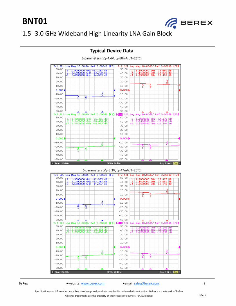
Typical Device Data
S-parameters (Vd=4.4V, Id=68mA , T=25°C)
S-parameters (Vd=3.3V, Id=47mA, T=25°C)

4
Rev. E
BeRex website: www.berex.com email: [email protected]
Specifications and information are subject to change and products may be discontinued without notice. BeRex is a trademark of BeRex.
All other trademarks are the property of their respective owners. © 2018 BeRex
1.5 -3.0 GHz Wideband High Linearity LNA Gain Block
BNT01
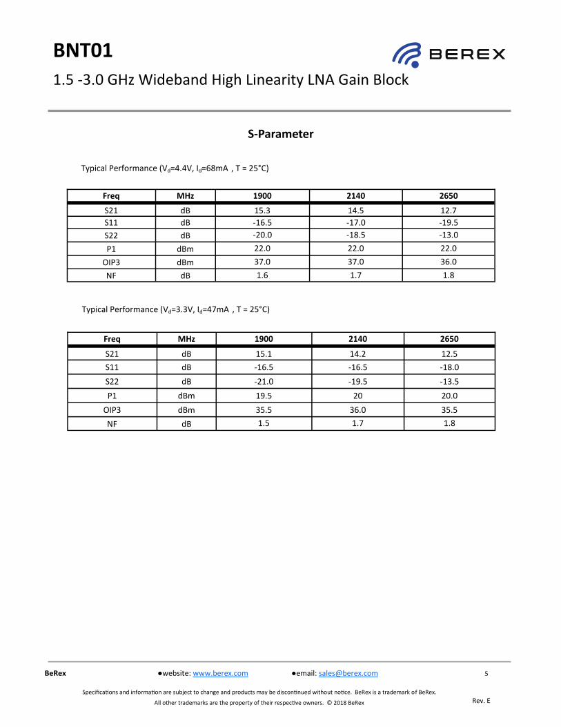
S-Parameter
(Vd=4.4V,Id = 68mA, T = 25 °C, calibrated to device leads)
Freq
[MHz]
S11
Mag
S11
Ang
S21
Mag
S21
Ang
S12
Mag
S12
Ang
S22
Mag
S22
Ang
1500 0.21 155.96 7.19 90.39 0.07 28.60 0.22 73.75
2000 0.23 145.09 5.83 72.67 0.09 26.29 0.18 59.00
2500 0.23 133.56 4.90 57.27 0.11 20.75 0.14 40.48
3000 0.23 118.22 4.22 42.87 0.13 14.03 0.11 23.19
3500 0.26 102.19 3.71 29.21 0.15 6.66 0.11 16.14
4000 0.30 88.92 3.34 15.62 0.16 -1.45 0.11 23.35
(Vd=3.3V,Id = 47mA, T = 25 °C, calibrated to device leads)
Freq
[MHz]
S11
Mag
S11
Ang
S21
Mag
S21
Ang
S12
Mag
S12
Ang
S22
Mag
S22
Ang
1500 0.21 162.00 7.01 91.01 0.07 27.71 0.20 76.38
2000 0.24 148.94 5.70 73.25 0.09 26.75 0.17 63.05
2500 0.24 136.58 4.79 57.65 0.11 21.42 0.13 45.92
3000 0.24 121.21 4.14 43.10 0.13 13.96 0.11 29.25
3500 0.27 104.45 3.65 29.40 0.15 6.26 0.10 23.24
4000 0.30 90.91 3.28 15.83 0.17 -1.81 0.11 31.06
5
Rev. E
BeRex website: www.berex.com email: [email protected]
Specifications and information are subject to change and products may be discontinued without notice. BeRex is a trademark of BeRex.
All other trademarks are the property of their respective owners. © 2018 BeRex
1.5 -3.0 GHz Wideband High Linearity LNA Gain Block
BNT01
S-Parameter
Typical Performance (Vd=4.4V, Id=68mA , T = 25°C)
Typical Performance (Vd=3.3V, Id=47mA , T = 25°C)
Freq MHz 1900 2140 2650
S21 dB 15.3 14.5 12.7
S11 dB -16.5 -17.0 -19.5
S22 dB -20.0 -18.5 -13.0
P1 dBm 22.0 22.0 22.0
OIP3 dBm 37.0 37.0 36.0
NF dB 1.6 1.7 1.8
Freq MHz 1900 2140 2650
S21 dB 15.1 14.2 12.5
S11 dB -16.5 -16.5 -18.0
S22 dB -21.0 -19.5 -13.5
P1 dBm 19.5 20 20.0
OIP3 dBm 35.5 36.0 35.5
NF dB 1.5 1.7 1.8

6
Rev. E
BeRex website: www.berex.com email: [email protected]
Specifications and information are subject to change and products may be discontinued without notice. BeRex is a trademark of BeRex.
All other trademarks are the property of their respective owners. © 2018 BeRex
1.5 -3.0 GHz Wideband High Linearity LNA Gain Block
BNT01
WCDMA 4FA 2140MHz -50dBc (Vd=4.4V)
WCDMA 4FA 2140MHz -50dBc (Vd=3.3V)

7
Rev. E
BeRex website: www.berex.com email: [email protected]
Specifications and information are subject to change and products may be discontinued without notice. BeRex is a trademark of BeRex.
All other trademarks are the property of their respective owners. © 2018 BeRex
1.5 -3.0 GHz Wideband High Linearity LNA Gain Block
BNT01
WCDMA 6FA 2140MHz -50dBc (Vd=4.4V)
WCDMA 6FA 2140MHz -50dBc (Vd=3.3V)

8
Rev. E
BeRex website: www.berex.com email: [email protected]
Specifications and information are subject to change and products may be discontinued without notice. BeRex is a trademark of BeRex.
All other trademarks are the property of their respective owners. © 2018 BeRex
1.5 -3.0 GHz Wideband High Linearity LNA Gain Block
BNT01
LTE TM3p1 100% 20MHz 1850MHz -50dBc (Vd=4.4V)
LTE TM3p1 100% 20MHz 1850MHz -50dBc (Vd=3.3V)
9
Rev. E
BeRex website: www.berex.com email: [email protected]
Specifications and information are subject to change and products may be discontinued without notice. BeRex is a trademark of BeRex.
All other trademarks are the property of their respective owners. © 2018 BeRex
1.5 -3.0 GHz Wideband High Linearity LNA Gain Block
BNT01
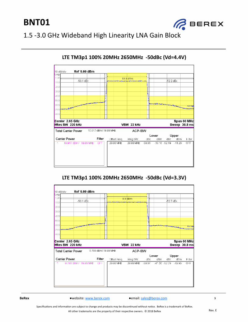
LTE TM3p1 100% 20MHz 2650MHz -50dBc (Vd=4.4V)
LTE TM3p1 100% 20MHz 2650MHz -50dBc (Vd=3.3V)

10
Rev. E
BeRex website: www.berex.com email: [email protected]
Specifications and information are subject to change and products may be discontinued without notice. BeRex is a trademark of BeRex.
All other trademarks are the property of their respective owners. © 2018 BeRex
1.5 -3.0 GHz Wideband High Linearity LNA Gain Block
BNT01
Device Performance
Pin-Pout-Gain
Vd = 4.4V, Id = 68mA
Vd = 3.3V, Id = 47mA

11
Rev. E
BeRex website: www.berex.com email: [email protected]
Specifications and information are subject to change and products may be discontinued without notice. BeRex is a trademark of BeRex.
All other trademarks are the property of their respective owners. © 2018 BeRex
1.5 -3.0 GHz Wideband High Linearity LNA Gain Block
BNT01
OIP3
Vd = 4.4V, Id = 68mA

12
Rev. E
BeRex website: www.berex.com email: [email protected]
Specifications and information are subject to change and products may be discontinued without notice. BeRex is a trademark of BeRex.
All other trademarks are the property of their respective owners. © 2018 BeRex
1.5 -3.0 GHz Wideband High Linearity LNA Gain Block
BNT01
OIP3
Vd = 3.3V, Id = 47mA

13
Rev. E
BeRex website: www.berex.com email: [email protected]
Specifications and information are subject to change and products may be discontinued without notice. BeRex is a trademark of BeRex.
All other trademarks are the property of their respective owners. © 2018 BeRex
1.5 -3.0 GHz Wideband High Linearity LNA Gain Block
BNT01
ACLR
Vd = 4.4V, Id = 68mA

14
Rev. E
BeRex website: www.berex.com email: [email protected]
Specifications and information are subject to change and products may be discontinued without notice. BeRex is a trademark of BeRex.
All other trademarks are the property of their respective owners. © 2018 BeRex
1.5 -3.0 GHz Wideband High Linearity LNA Gain Block
BNT01
ACLR
Vd = 3.3V, Id = 47mA

15
Rev. E
BeRex website: www.berex.com email: [email protected]
Specifications and information are subject to change and products may be discontinued without notice. BeRex is a trademark of BeRex.
All other trademarks are the property of their respective owners. © 2018 BeRex
1.5 -3.0 GHz Wideband High Linearity LNA Gain Block
BNT01
Gain Flatness
Vd = 4.4V, Id = 68mA
Vd = 3.3V, Id = 47mA

16
Rev. E
BeRex website: www.berex.com email: [email protected]
Specifications and information are subject to change and products may be discontinued without notice. BeRex is a trademark of BeRex.
All other trademarks are the property of their respective owners. © 2018 BeRex
1.5 -3.0 GHz Wideband High Linearity LNA Gain Block
BNT01
Package Outline Dimension
Suggested PCB Land Pattern and PAD Layout
PCB Land Pattern PCB Mounting
Note : All dimension _ millimeters
PCB lay out _ on BeRex website
0.75
1.20
1.20
1.20
1.50
1.300.40 0.40
Ø0.40
2.15
2.80
0.40
0.50
1.00
1.20
0.65
0.45
0.35

17
Rev. E
BeRex website: www.berex.com email: [email protected]
Specifications and information are subject to change and products may be discontinued without notice. BeRex is a trademark of BeRex.
All other trademarks are the property of their respective owners. © 2018 BeRex
1.5 -3.0 GHz Wideband High Linearity LNA Gain Block
BNT01
Lead plating finish
100% Tin Matte finish
(All BeRex products undergoes a 1 hour, 150 degree C, Anneal bake to eliminate thin whisker growth concerns.)
MSL / ESD Rating
ESD Rating:
Value:
Test:
Standard:
MSL Rating:
Standard:
Class 1A
Passes <500V
Human Body Model (HBM)
JEDEC Standard JESD22-A114B
Level 1 at +265°C convection reflow
JEDEC Standard J-STD-020
NATO CAGE code:
2 N 9 6 F
Tape & Reel
SOT89 Packaging information:
Tape Width (mm): 12
Reel Size (inches): 7
Device Cavity Pitch (mm): 8
Devices Per Reel: 1000
Package Marking
YY = Year, WW = Working Week,
XX = Wafer No.