13. Configuring Cyclone FPGAs - intel.com · nCE nCEO N.C. Decompression Controller Cyclone FPGA...
52
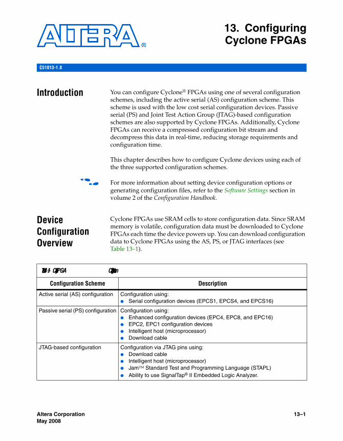
Altera Corporation 13–1 May 2008 13. Configuring Cyclone FPGAs Introduction You can configure Cyclone ® FPGAs using one of several configuration schemes, including the active serial (AS) configuration scheme. This scheme is used with the low cost serial configuration devices. Passive serial (PS) and Joint Test Action Group (JTAG)-based configuration schemes are also supported by Cyclone FPGAs. Additionally, Cyclone FPGAs can receive a compressed configuration bit stream and decompress this data in real-time, reducing storage requirements and configuration time. This chapter describes how to configure Cyclone devices using each of the three supported configuration schemes. f For more information about setting device configuration options or generating configuration files, refer to the Software Settings section in volume 2 of the Configuration Handbook. Device Configuration Overview Cyclone FPGAs use SRAM cells to store configuration data. Since SRAM memory is volatile, configuration data must be downloaded to Cyclone FPGAs each time the device powers up. You can download configuration data to Cyclone FPGAs using the AS, PS, or JTAG interfaces (see Table 13–1). Tab le 13– 1. Cy c l o n e FPGA Co n f i g u r a t i o n Sc h e m e s Configuration Scheme Description Active serial (AS) configuration Configuration using: ● Serial configuration devices (EPCS1, EPCS4, and EPCS16) Passive serial (PS) configuration Configuration using: ● Enhanced configuration devices (EPC4, EPC8, and EPC16) ● EPC2, EPC1 configuration devices ● Intelligent host (microprocessor) ● Download cable JTAG-based configuration Configuration via JTAG pins using: ● Download cable ● Intelligent host (microprocessor) ● Jam TM Standard Test and Programming Language (STAPL) ● Ability to use SignalTap ® II Embedded Logic Analyzer. C51013-1.8
Transcript of 13. Configuring Cyclone FPGAs - intel.com · nCE nCEO N.C. Decompression Controller Cyclone FPGA...
Altera Corporation 13–1May 2008
13. ConfiguringCyclone FPGAs
Introduction You can configure Cyclone® FPGAs using one of several configuration schemes, including the active serial (AS) configuration scheme. This scheme is used with the low cost serial configuration devices. Passive serial (PS) and Joint Test Action Group (JTAG)-based configuration schemes are also supported by Cyclone FPGAs. Additionally, Cyclone FPGAs can receive a compressed configuration bit stream and decompress this data in real-time, reducing storage requirements and configuration time.
This chapter describes how to configure Cyclone devices using each of the three supported configuration schemes.
f For more information about setting device configuration options or generating configuration files, refer to the Software Settings section in volume 2 of the Configuration Handbook.
Device Configuration Overview
Cyclone FPGAs use SRAM cells to store configuration data. Since SRAM memory is volatile, configuration data must be downloaded to Cyclone FPGAs each time the device powers up. You can download configuration data to Cyclone FPGAs using the AS, PS, or JTAG interfaces (see Table 13–1).
Table 13–1. Cyclone FPGA Configuration Schemes
Configuration Scheme Description
Active serial (AS) configuration Configuration using:● Serial configuration devices (EPCS1, EPCS4, and EPCS16)
Passive serial (PS) configuration Configuration using:● Enhanced configuration devices (EPC4, EPC8, and EPC16)● EPC2, EPC1 configuration devices● Intelligent host (microprocessor)● Download cable
JTAG-based configuration Configuration via JTAG pins using:● Download cable● Intelligent host (microprocessor)● JamTM Standard Test and Programming Language (STAPL)● Ability to use SignalTap® II Embedded Logic Analyzer.
C51013-1.8

13–2 Altera CorporationCyclone Device Handbook, Volume 1 May 2008
Device Configuration Overview
You can select a Cyclone FPGA configuration scheme by driving its MSEL1 and MSEL0 pins either high (1) or low (0), as shown in Table 13–2. If your application only requires a single configuration mode, the MSEL pins can be connected to VCC (the I/O bank’s VCCIO voltage where the MSEL pin resides) or to ground. If your application requires more than one configuration mode, the MSEL pins can be switched after the FPGA has been configured successfully. Toggling these pins during user mode does not affect the device operation. However, the MSEL pins must be valid before initiating reconfiguration.
After configuration, Cyclone FPGAs will initialize registers and I/O pins, then enter user mode and function as per the user design. Figure 13–1 shows an AS configuration waveform.
Figure 13–1. AS Configuration Waveform
Table 13–2. Selecting Cyclone Configuration Schemes
MSEL1 MSEL0 Configuration Scheme
0 0 AS
0 1 PS
0 1 JTAG-based (1)
Note to Table 13–2:(1) JTAG-based configuration takes precedence over other schemes, which means
that MSEL pin settings are ignored.
Read Address
136 Cycles
nSTATUS
nCONFIG
CONF_DONE
nCSO
DCLK
ASDO
DATA0
INIT_DONE
User I/O User Mode
Tri-stated with internalpull-up resistor.
bit N − 1bit N bit 1 bit 0

Altera Corporation 13–3May 2008 Cyclone Device Handbook, Volume 1
Configuring Cyclone FPGAs
You can configure Cyclone FPGAs using the 3.3-, 2.5-, 1.8-, or 1.5-V LVTTL I/O standard on configuration and JTAG input pins. These devices do not feature a VCCSEL pin; therefore, you should connect the VCCIO pins of the I/O banks containing configuration or JTAG pins according to the I/O standard specifications.
Table 13–3 summarizes the approximate uncompressed configuration file size for each Cyclone FPGA. To calculate the amount of storage space required for multi-device configurations, add the file size of each device together.
You should only use the numbers in Table 13–3 to estimate the configuration file size before design compilation. Different file formats, such as .hex or .ttf files, have different file sizes. For any specific version of the Quartus® II software, any design targeted for the same device has the same uncompressed configuration file size. If compression is used, the file size can vary after each compilation.
Data Compression
Cyclone FPGAs are the first FPGAs to support decompression of configuration data. This feature allows you to store compressed configuration data in configuration devices or other memory, and transmit this compressed bit stream to Cyclone FPGAs. During configuration, the Cyclone FPGA decompresses the bit stream in real time and programs its SRAM cells.
Cyclone FPGAs support compression in the AS and PS configuration schemes. Compression is not supported for JTAG-based configuration.
1 Preliminary data indicates that compression reduces configuration bit stream size by 35 to 60%.
Table 13–3. Cyclone Raw Binary File (.rbf) Sizes
Device Data Size (Bits) Data Size (Bytes)
EP1C3 627,376 78,422
EP1C4 924,512 115,564
EP1C6 1,167,216 145,902
EP1C12 2,323,240 290,405
EP1C20 3,559,608 435,000

13–4 Altera CorporationCyclone Device Handbook, Volume 1 May 2008
Data Compression
When you enable compression, the Quartus II software generates configuration files with compressed configuration data. This compression reduces the storage requirements in the configuration device or flash, and decreases the time needed to transmit the bit stream to the Cyclone FPGA.
There are two methods to enable compression for Cyclone bitstreams: before design compilation (in the Compiler Settings menu) and after design compilation (in the Convert Programming Files window).
To enable compression in the project's compiler settings, select Device under the Assignments menu to bring up the settings window. After selecting your Cyclone device open the Device and Pin Options window, and in the General settings tab enable the check box for Generate compressed bitstreams (as shown in Figure 13–2).

Altera Corporation 13–5May 2008 Cyclone Device Handbook, Volume 1
Configuring Cyclone FPGAs
Figure 13–2. Enabling Compression for Cyclone Bitstreams in Compiler Settings
13–6 Altera CorporationCyclone Device Handbook, Volume 1 May 2008
Data Compression
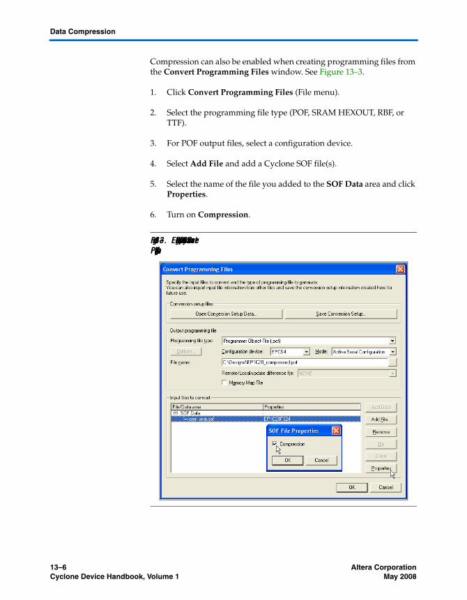
Compression can also be enabled when creating programming files from the Convert Programming Files window. See Figure 13–3.
1. Click Convert Programming Files (File menu).
2. Select the programming file type (POF, SRAM HEXOUT, RBF, or TTF).
3. For POF output files, select a configuration device.
4. Select Add File and add a Cyclone SOF file(s).
5. Select the name of the file you added to the SOF Data area and click Properties.
6. Turn on Compression.
Figure 13–3. Enabling Compression for Cyclone Bitstreams in Convert Programming Files
Altera Corporation 13–7May 2008 Cyclone Device Handbook, Volume 1
Configuring Cyclone FPGAs
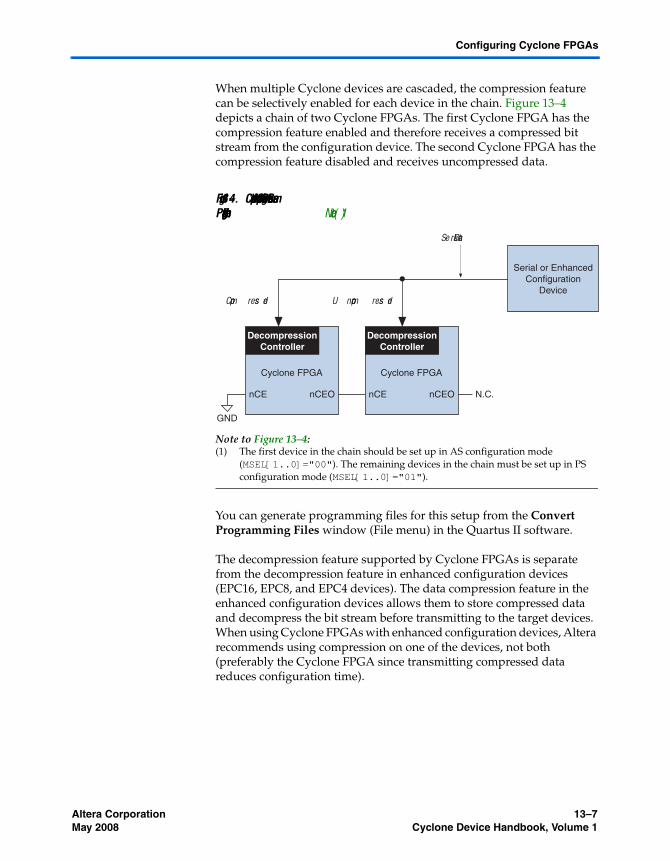
When multiple Cyclone devices are cascaded, the compression feature can be selectively enabled for each device in the chain. Figure 13–4 depicts a chain of two Cyclone FPGAs. The first Cyclone FPGA has the compression feature enabled and therefore receives a compressed bit stream from the configuration device. The second Cyclone FPGA has the compression feature disabled and receives uncompressed data.
Figure 13–4. Compressed and Uncompressed Configuration Data in the Same Programming File Note (1)
Note to Figure 13–4:(1) The first device in the chain should be set up in AS configuration mode
(MSEL[1..0]="00"). The remaining devices in the chain must be set up in PS configuration mode (MSEL[1..0]="01").
You can generate programming files for this setup from the Convert Programming Files window (File menu) in the Quartus II software.
The decompression feature supported by Cyclone FPGAs is separate from the decompression feature in enhanced configuration devices (EPC16, EPC8, and EPC4 devices). The data compression feature in the enhanced configuration devices allows them to store compressed data and decompress the bit stream before transmitting to the target devices. When using Cyclone FPGAs with enhanced configuration devices, Altera recommends using compression on one of the devices, not both (preferably the Cyclone FPGA since transmitting compressed data reduces configuration time).
nCE
GND
nCEO
DecompressionController
Cyclone FPGA
nCE nCEO N.C.
DecompressionController
Cyclone FPGA
Serial or EnhancedConfiguration
Device
Serial Data
Compressed Uncompressed

13–8 Altera CorporationCyclone Device Handbook, Volume 1 May 2008
Configuration Schemes
Configuration Schemes
This section describes the various configuration schemes you can use to configure Cyclone FPGAs. Descriptions include an overview of the protocol, pin connections, and timing information. The schemes discussed are:
■ AS configuration (serial configuration devices)■ PS configuration■ JTAG-based configuration
Active Serial Configuration (Serial Configuration Devices)
In the AS configuration scheme, Cyclone FPGAs are configured using the new serial configuration devices. These configuration devices are low cost devices with non-volatile memory that feature a simple four-pin interface and a small form factor. These features make serial configuration devices an ideal solution for configuring the low-cost Cyclone FPGAs.
f For more information on programming serial configuration devices, refer to the Cyclone Literature web page at www.altera.com and the Serial Configuration Devices (EPCS1, EPCS4, EPCS16, EPCS64, and EPCS128) Data Sheet.
Serial configuration devices provide a serial interface to access configuration data. During device configuration, Cyclone FPGAs read configuration data via the serial interface, decompress data if necessary, and configure their SRAM cells. This scheme is referred to as an AS configuration scheme because the FPGA controls the configuration interface. This scheme is in contrast to the PS configuration scheme where the configuration device controls the interface.
Serial configuration devices have a four-pin interface: serial clock input (DCLK), serial data output (DATA), AS data input (ASDI), and an active-low chip select (nCS). This four-pin interface connects to Cyclone FPGA pins as shown in Figure 13–5.

Altera Corporation 13–9May 2008 Cyclone Device Handbook, Volume 1
Configuring Cyclone FPGAs
Figure 13–5. AS Configuration of a Single Cyclone FPGA
Notes to Figure 13–5: (1) Connect the pull-up resistors to a 3.3-V supply.(2) Cyclone FPGAs use the ASDO to ASDI path to control the configuration device.
Connecting the MSEL[1..0] pins to 00 selects the AS configuration scheme. The Cyclone chip enable signal, nCE, must also be connected to ground or driven low for successful configuration.
During system power up, both the Cyclone FPGA and serial configuration device enter a power-on reset (POR) period. As soon as the Cyclone FPGA enters POR, it drives nSTATUS low to indicate it is busy and drives CONF_DONE low to indicate that it has not been configured. After POR, which typically lasts 100 ms, the Cyclone FPGA releases nSTATUS and enters configuration mode when this signal is pulled high by the external 10-kΩ resistor. Once the FPGA successfully exits POR, all user I/O pins are tri-stated. Cyclone devices have weak pull-up resistors on the user I/O pins which are on before and during configuration.
f The value of the weak pull-up resistors on the I/O pins that are on before and during configuration can be found in the DC and Switching Characteristics chapter in the Cyclone Device Handbook.
The serial clock (DCLK) generated by the Cyclone FPGA controls the entire configuration cycle (see Figure 13–1 on page 13–2) and this clock signal provides the timing for the serial interface. Cyclone FPGAs use an
GND
N.C.
DATA
DCLK
nCS
ASDI
DATA0
DCLK
nCSO
ASDO
Serial ConfigurationDevice Cyclone FPGA
10 kΩ10 kΩ
VCC
10 kΩ
VCC VCC
GND
nCEO
nCE
nSTATUS
nCONFIGCONF_DONE
(2)
MSEL1
MSEL0
(1) (1) (1)

13–10 Altera CorporationCyclone Device Handbook, Volume 1 May 2008
Configuration Schemes
internal oscillator to generate DCLK. After configuration, this internal oscillator is turned off. Table 13–4 shows the active serial DCLK output frequencies.
The serial configuration device latches input/control signals on the rising edge of DCLK and drives out configuration data on the falling edge. Cyclone FPGAs drive out control signals on the falling edge of DCLK and latch configuration data on the falling edge of DCLK.
In configuration mode, the Cyclone FPGA enables the serial configuration device by driving its nCSO output pin low that is connected to the chip select (nCS) pin of the configuration device. The Cyclone FPGA’s serial clock (DCLK) and serial data output (ASDO) pins send operation commands and read-address signals to the serial configuration device. The configuration device provides data on its serial data output (DATA) pin that is connected to the DATA0 input on Cyclone FPGAs.
After the Cyclone FPGA receives all configuration bits, it releases the open-drain CONF_DONE pin allowing the external 10-kΩ resistor to pull this signal to a high level. Initialization begins only after the CONF_DONE line reaches a high level. The CONF_DONE pin must have an external 10-kΩ pull-up resistor in order for the device to initialize.
You can select the clock used for initialization by using the User Supplied Start-Up Clock option in the Quartus II software. The Quartus II software uses the 10-MHz (typical) internal oscillator (separate from the AS internal oscillator) by default to initialize the Cyclone FPGA. After initialization, the internal oscillator is turned off. When you enable the User Supplied Start-Up Clock option, the software uses the CLKUSR pin as the initialization clock. Supplying a clock on the CLKUSR pin does not affect the configuration process. After all configuration data is accepted and the CONF_DONE signal goes high, Cyclone devices require 136 clock cycles to initialize properly.
An optional INIT_DONE pin is available. This pin signals the end of initialization and the start of user mode with a low-to-high transition. The Enable INIT_DONE output option is available in the Quartus II software. If the INIT_DONE pin is used, it is high due to an external 10-kΩ pull-up resistor when nCONFIG is low and during the beginning of configuration. Once the option bit to enable INIT_DONE is programmed into the device (during the first frame of configuration data), the
Table 13–4. Active Serial DCLK Output Frequency
Minimum Typical Maximum Units
14 17 20 MHz

Altera Corporation 13–11May 2008 Cyclone Device Handbook, Volume 1
Configuring Cyclone FPGAs
INIT_DONE pin goes low. When initialization is complete, the INIT_DONE pin is released and pulled high. This low-to-high transition signals that the FPGA has entered user mode. In user mode, the user I/O pins do not have weak pull-ups and functions as assigned in your design.
If an error occurs during configuration, the Cyclone FPGA asserts the nSTATUS signal low indicating a data frame error, and the CONF_DONE signal stays low. With the Auto-Restart Configuration on Frame Error option enabled in the Quartus II software, the Cyclone FPGA resets the configuration device by pulsing nCSO, releases nSTATUS after a reset time-out period (about 30 μs), and retries configuration. If this option is turned off, the system must monitor nSTATUS for errors and then pulse nCONFIG low for at least 40 μs to restart configuration. After successful configuration, the CONF_DONE signal is tri-stated by the target device and then pulled high by the pull-up resistor.
All AS configuration pins, DATA0, DCLK, nCSO, and ASDO, have weak internal pull-up resistors. These pull-up resistors are always active.
When the Cyclone FPGA is in user mode, you can initiate reconfiguration by pulling the nCONFIG pin low. The nCONFIG pin should be low for at least 40 μs. When nCONFIG is pulled low, the FPGA also pulls nSTATUS and CONF_DONE low and all I/O pins are tri-stated. Once nCONFIG returns to a logic high level and nSTATUS is released by the Cyclone FPGA, reconfiguration begins.
Configuring Multiple Devices (Cascading)
You can configure multiple Cyclone FPGAs using a single serial configuration device. You can cascade multiple Cyclone FPGAs using the chip-enable (nCE) and chip-enable-out (nCEO) pins. The first device in the chain must have its nCE pin connected to ground. You must connect its nCEO pin to the nCE pin of the next device in the chain. When the first device captures all of its configuration data from the bit stream, it drives the nCEO pin low enabling the next device in the chain. You must leave the nCEO pin of the last device unconnected. The nCONFIG, nSTATUS, CONF_DONE, DCLK, and DATA0 pins of each device in the chain are connected (see Figure 13–6).
This first Cyclone FPGA in the chain is the configuration master and controls configuration of the entire chain. You must connect its MSEL pins to select the AS configuration scheme. The remaining Cyclone FPGAs are configuration slaves and you must connect their MSEL pins to select the PS configuration scheme. Figure 13–6 shows the pin connections for this setup.

13–12 Altera CorporationCyclone Device Handbook, Volume 1 May 2008
Configuration Schemes
Figure 13–6. Configuring Multiple Devices Using a Serial Configuration Device (AS)
Note to Figure 13–6: (1) Connect the pull-up resistors to a 3.3-V supply.
As shown in Figure 13–6, the nSTATUS and CONF_DONE pins on all target FPGAs are connected together with external pull-up resistors. These pins are open-drain bidirectional pins on the FPGAs. When the first device asserts nCEO (after receiving all of its configuration data), it releases its CONF_DONE pin. But the subsequent devices in the chain keep this shared CONF_DONE line low until they have received their configuration data. When all target FPGAs in the chain have received their configuration data and have released CONF_DONE, the pull-up resistor drives a high level on this line and all devices simultaneously enter initialization mode. If an error occurs at any point during configuration, the nSTATUS line is driven low by the failing FPGA. If you enable the Auto Restart Configuration on Frame Error option, reconfiguration of the entire chain begins after a reset time-out period (a maximum of 40 μs). If the option is turned off, the external system must monitor nSTATUS for errors and then pulse nCONFIG low to restart configuration. The external system can pulse nCONFIG if it is under system control rather than tied to VCC.
1 While you can cascade Cyclone FPGAs, serial configuration devices cannot be cascaded or chained together.
DATA
DCLK
nCS
ASDI
DATA0
DCLK
nCSO
ASDO
Serial ConfigurationDevice Cyclone FPGA Master
10 kΩ10 kΩ
VCC VCC
GND
nCEOnCE
nSTATUSCONF_DONE
DATA0
DCLK
Cyclone FPGA Slave
nCEO
nCE
nSTATUSCONF_DONE
10 kΩ
VCC
nCONFIG nCONFIG
MSEL1
MSEL0
GND
VCC
N.C.
MSEL1
MSEL0
GND
(1) (1) (1)
Altera Corporation 13–13May 2008 Cyclone Device Handbook, Volume 1
Configuring Cyclone FPGAs
If the configuration bit stream size exceeds the capacity of a serial configuration device, you must select a larger configuration device and/or enable the compression feature. While configuring multiple devices, the size of the bit stream is the sum of the individual devices’ configuration bit streams.
Configuring Multiple Devices with the Same Data
Certain applications require the configuration of multiple Cyclone devices with the same design through a configuration bit stream or SOF file. This can actually be done by two methods and they are shown below. For both methods, the serial configuration devices cannot be cascaded or chained together.
Method 1For method 1, the serial configuration device stores two copies of the SOF file. The first copy configures the master Cyclone device, and the second copy configures all the remaining slave devices concurrently. The setup is similar to Figure 13–7 where the master is setup in AS mode (MSEL=00) and the slave devices are setup in PS mode (MSEL01).
To configure four identical Cyclone devices with the same SOF file, you could setup the chain similar to the example shown in Figure 13–6, except connect the three slave devices for concurrent configuration. The nCEO pin from the master device drives the nCE input pins on all three slave devices, and the DATA and DCLK pins connect in parallel to all four devices. During the first configuration cycle, the master device reads its configuration data from the serial configuration device while holding nCEO high. After completing its configuration cycle, the master drives nCE low and transmits the second copy of the configuration data to all three slave devices, configuring them simultaneously. The advantage of using the setup in Figure 13–7 is you can have a different SOF file for the Cyclone master device. However, all the Cyclone slave devices must be configured with the same SOF file.

13–14 Altera CorporationCyclone Device Handbook, Volume 1 May 2008
Configuration Schemes
Figure 13–7. Configuring Multiple Devices with the Same Design Using a Serial Configuration Device
Note to Figure 13–7:(1) The pull-up resistor should be connected to the same supply voltage as the configuration device.
Method 2Method 2 configures multiple Cyclone devices with the same SOFs by storing only one copy of the SOF in the serial configuration device. This saves memory space in the serial configuration device for general-purpose use and may reduce costs. This method is shown in Figure 13–8 where the master device is set up in AS mode (MSLE=00), and
MSEL0
MSEL1
SerialConfiguration
Device
Data
DCLK
nCS
ASDI
nSTATUS
CONF_DONE
nCONFIG
nCE
Data0
DCLK
nCSO
ASDO
GND
10 kΩ 10 kΩ 10 kΩ
VCC (1)
GND
nCEO
GND
VCC
nSTATUS
CONF_DONE
nCONFIG
nCE
Data0
DCLKMSEL0
MSEL1
nCEO N.C.
Cyclone FPGA Slave
GND
VCC
nSTATUS
CONF_DONE
nCONFIG
nCE
Data0
DCLKMSEL0
MSEL1
nCEO N.C.
Cyclone FPGA Slave
GND
VCC
nSTATUS
CONF_DONE
nCONFIG
nCE
Data0
DCLKMSEL0
MSEL1
nCEO N.C.
Cyclone FPGA Slave
Cyclone FPGA Master

Altera Corporation 13–15May 2008 Cyclone Device Handbook, Volume 1
Configuring Cyclone FPGAs
the slave devices are set up in PS mode (MSEL=01). You could set up one or more slave devices in the chain and all the slave devices are set up in the same way as the design shown in Figure 13–8.
Figure 13–8. Configuring Multiple Devices with the Same Design Using a Serial Configuration Device
In this setup, all the Cyclone devices in the chain are connected for concurrent configuration. This reduces the active serial configuration time because all the Cyclone devices are configured in only one configuration cycle. To achieve this, the nCE input pins on all the Cyclone devices are connected to ground and the nCEO output pins on all the Cyclone devices are left unconnected. The DATA and DCLK pins connect in parallel to all the Cyclone devices.
It is recommended to add a buffer before the DATA and DCLK output from the master Cyclone to avoid signal strength and signal integrity issues. The buffer should not significantly change the DATA-to-DCLK relationships or delay them with respect to other ASMI signals, which are
nSTATUS
CONF_DONE
nCONFIG
nCE
Data0
DCLK
nCS0
MSEL0
MSEL1
EPCS4Device
Data
DCLK
nCS
ASDI ASDO
GND
10 kΩ 10 kΩ 10 kΩ
VCC
Buffer
GND
Master Cyclone Device
GND
nSTATUS
CONF_DONE
nCONFIG
nCE
Data0
DCLK
nCS0
MSEL0
MSEL1
ASDO GND
VCC
Slave Cyclone Device

13–16 Altera CorporationCyclone Device Handbook, Volume 1 May 2008
Configuration Schemes
ASDI and nCS signals. Also, the buffer should only drive the slave Cyclone devices, so that the timing between the master Cyclone device and serial configuration device is unaffected.
This setup can support both compressed and uncompressed SOFs. Therefore, if the configuration bit stream size exceeds the capacity of a serial configuration device, you can enable the compression feature on the SOF used or you can select a larger serial configuration device.
Estimating Active Serial Configuration Time
Active serial configuration time is dominated by the time it takes to transfer data from the serial configuration device to the Cyclone FPGA. This serial interface is clocked by the Cyclone DCLK output (generated from an internal oscillator). As listed in Table 13–4, the DCLK minimum frequency is 14 MHz (71 ns). Therefore, the maximum configuration time estimate for an EP1C3 device (0.628 MBits of uncompressed data) is:
(0.628 MBits × 71 ns) = 47 ms.
The typical configuration time is 33 ms.
Enabling compression reduces the amount of configuration data that is transmitted to the Cyclone device, reducing configuration time. On average, compression reduces configuration time by 50%.
Programming Serial Configuration Devices
Serial configuration devices are non-volatile, flash-memory-based devices. You can program these devices in-system using the ByteBlasterTM II download cable. Alternatively, you can program them using the Altera Programming Unit (APU) or supported third-party programmers.
You can perform in-system programming of serial configuration devices via the AS programming interface. During in-system programming, the download cable disables FPGA access to the AS interface by driving the nCE pin high. Cyclone FPGAs are also held in reset by a low level on nCONFIG. After programming is complete, the download cable releases nCE and nCONFIG, allowing the pull-down and pull-up resistor to drive GND and VCC, respectively. Figure 13–9 shows the download cable connections to the serial configuration device.
f For more information about the ByteBlaster II cable, refer to the ByteBlaster II Download Cable User Guide.

Altera Corporation 13–17May 2008 Cyclone Device Handbook, Volume 1
Configuring Cyclone FPGAs
The serial configuration devices can be programmed in-system by an external microprocessor using SRunner. SRunner is a software driver developed for embedded serial configuration device programming that can be customized to fit in different embedded systems. The SRunner can read a Raw Programming Data file (.rpd) and write to the serial configuration devices. The programming time is comparable to the Quartus II software programming time.
f For more information about SRunner, refer tothe AN 418: SRunner: An Embedded Solution for Serial Configuration Device Programming and the source code on the Altera website (www.altera.com).
Figure 13–9. In-System Programming of Serial Configuration Devices
Notes to Figure 13–9:(1) Connect these pull-up resistors to 3.3-V supply.(2) The nCEO pin is left unconnected.(3) Power up the ByteBlaster II cable’s VCC with a 3.3-V supply.
DATA
DCLK
nCS
ASDI
DATA0
DCLK
nCSO
nCE
nCONFIG
nSTATUS nCEO
CONF_DONE
ASDO
VCC VCC VCC
VCC
10 kΩ 10 kΩ 10 kΩ
10 kΩ
Cyclone FPGA
SerialConfiguration
Device
Pin 1
MSEL1
MSEL0
GND
ByteBlaser II 10-Pin Male Header
(2)N.C.
(1) (1) (1)
(3)

13–18 Altera CorporationCyclone Device Handbook, Volume 1 May 2008
Configuration Schemes
You can program serial configuration devices by using the Quartus II software with the APU and the appropriate configuration device programming adapter. All serial configuration devices are offered in an eight-pin small outline integrated circuit (SOIC) package and can be programmed using the PLMSEPC-8 adapter.
In production environments, serial configuration devices can be programmed using multiple methods. Altera programming hardware (APU) or other third-party programming hardware can be used to program blank serial configuration devices before they are mounted onto PCBs. Alternatively, you can use an on-board microprocessor to program the serial configuration device in-system using C-based software drivers provided by Altera.
f For more information on programming serial configuration devices, refer to the Cyclone Literature web page at www.altera.com and the Serial Configuration Devices (EPCS1, EPCS4, EPCS16, EPCS64, and EPCS128) Data Sheet.
f Device configuration options and how to create configuration files are discussed further in the Software Settings section in volume 2 of the Configuration Handbook.
Passive Serial Configuration
Cyclone FPGAs also feature the PS configuration scheme supported by all Altera FPGAs. In the PS scheme, an external host (configuration device, embedded processor, or host PC) controls configuration. Configuration data is clocked into the target Cyclone FPGAs via the DATA0 pin at each rising edge of DCLK. The configuration waveforms for this scheme are shown in Figure 13–10.

Altera Corporation 13–19May 2008 Cyclone Device Handbook, Volume 1
Configuring Cyclone FPGAs
Figure 13–10. PS Configuration Cycle Waveform
Notes to Figure 13–10:(1) During initial power up and configuration, CONF_DONE is low. After configuration, CONF_DONE goes high to
indicate successful configuration. If the device is reconfigured, CONF_DONE goes low after nCONFIG is driven low.(2) User I/O pins are tri-stated during configuration. Cyclone FPGAs also have a weak pull-up resistor on I/O pins
during configuration. After initialization, the user I/O pins perform the function assigned in the user’s design.(3) When used, the optional INIT_DONE signal is high when nCONFIG is low before configuration and during the first
136 clock cycles of configuration.(4) In user mode, DCLK should be driven high or low when using the PS configuration scheme. When using the AS
configuration scheme, DCLK is a Cyclone output pin and should not be driven externally.(5) In user mode, DATA0 should be driven high or low.
PS Configuration Using Configuration Device
In the PS configuration device scheme, nCONFIG is usually tied to VCC (when using EPC16, EPC8, EPC4, or EPC2 devices, you can connect nCONFIG to nINIT_CONF). Upon device power-up, the target Cyclone FPGA senses the low-to-high transition on nCONFIG and initiates configuration. The target device then drives the open-drain CONF_DONE pin low, which in-turn drives the configuration device’s nCS pin low. When exiting POR, both the target and configuration device release the open-drain nSTATUS pin (typically Cyclone POR lasts 100 ms).
Before configuration begins, the configuration device goes through a POR delay of up to 100 ms (maximum) to allow the power supply to stabilize. You must power the Cyclone FPGA before or during the POR time of the enhanced configuration device. During POR, the configuration device drives its OE pin low. This low signal delays configuration because the OE pin is connected to the target device’s nSTATUS pin. When the target and configuration devices complete POR, they both release the nSTATUS to OE line, which is then pulled high by a pull-up resistor.
High-Z
nCONFIG
nSTATUS
CONF_DONE (1)
DCLK
DATA
User I/O Pins (2)
INIT_DONE (3)
MODE
High-Z D0 D1 D2 D3
D(N – 1)
DN
Configuration Initialization User
User I/O
Configuration
(4)
(5)
Tri-stated with internal pull-up resistor

13–20 Altera CorporationCyclone Device Handbook, Volume 1 May 2008
Configuration Schemes
When configuring multiple devices, configuration does not begin until all devices release their OE or nSTATUS pins. When all devices are ready, the configuration device clocks out DATA and DCLK to the target devices using an internal oscillator.
After successful configuration, the Cyclone FPGA starts initialization using the 10-MHz internal oscillator as the reference clock. After initialization, this internal oscillator is turned off. The CONF_DONE pin is released by the target device and then pulled high by a pull-up resistor. When initialization is complete, the target Cyclone FPGA enters user mode. The CONF_DONE pin must have an external 10-kΩ pull-up resistor in order for the device to initialize.
If an error occurs during configuration, the target device drives its nSTATUS pin low, resetting itself internally and resetting the configuration device. If you turn on the Auto-Restart Configuration on Frame Error option, the device reconfigures automatically if an error occurs. To set this option, select Compiler Settings (Processing menu), and click on the Chips & Devices tab. Select Device and Pin Options, and click on the Configuration tab.
If the Auto-Restart Configuration on Frame Error option is turned off, the external system (configuration device or microprocessor) must monitor nSTATUS for errors and then pulse nCONFIG low to restart configuration. The external system can pulse nCONFIG if it is under system control rather than tied to VCC. When configuration is complete, the target device releases CONF_DONE, which disables the configuration device by driving nCS high. The configuration device drives DCLK low before and after configuration.
In addition, if the configuration device sends all of its data and then detects that CONF_DONE has not gone high, it recognizes that the target device has not configured successfully. (For CONF_DONE to reach a high state, enhanced configuration devices wait for 64 DCLK cycles after the last configuration bit. EPC2 devices wait for 16 DCLK cycles.) In this case, the configuration device pulses its OE pin low for a few microseconds, driving the target device’s nSTATUS pin low. If the Auto-Restart Configuration on Frame Error option is set in the Quartus II software, the target device resets and then releases its nSTATUS pin after a reset time-out period. When nSTATUS returns high, the configuration device reconfigures the target device.
You should not pull CONF_DONE low to delay initialization. Instead, use the Quartus II software’s User-Supplied Start-Up Clock option to synchronize the initialization of multiple devices that are not in the same configuration chain. Devices in the same configuration chain initialize together since their CONF_DONE pins are tied together.

Altera Corporation 13–21May 2008 Cyclone Device Handbook, Volume 1
Configuring Cyclone FPGAs
CONF_DONE goes high during the first few clock cycles of initialization. Hence, when using the CLKUSR feature you would not see the CONF_DONE signal high until you start clocking CLKUSR. However, the device does retain configuration data and waits for these initialization clocks to release CONF_DONE and go into user mode. Figure 13–11 shows how to configure one Cyclone FPGA with one configuration device.
Figure 13–11. Single Device Configuration Circuit
Notes to Figure 13–11:(1) The pull-up resistor should be connected to the same supply voltage as the
configuration device. This pull-up resistor is 10 kΩ. The EPC16, EPC8, EPC4, and EPC2 devices’ OE and nCS pins have internal, user-configurable pull-up resistors. If you use internal pull-up resistors, do not use external pull-up resistors on these pins.
(2) The nINIT_CONF pin is available on EPC16, EPC8, EPC4, and EPC2 devices and has an internal pull-up resistor that is always active. If nINIT_CONF is not used, nCONFIG can be pulled to VCC directly or through a resistor.
(3) The nCEO pin is left unconnected for the last device in the chain.(4) Connect MSEL0 to the VCC supply voltage of the I/O bank it resides in.
Configuring Multiple Cyclone FPGAs
You can use a single configuration device to configure multiple Cyclone FPGAs. In this setup, the nCEO pin of the first device is connected to the nCE pin of the second device in the chain. If there are additional devices, connect the nCE pin of the next device to the nCEO pin of the previous device. You should leave the nCEO pin on the last device in the chain unconnected. To configure properly, all of the target device CONF_DONE and nSTATUS pins must be tied together. Figure 13–12 shows an example of configuring multiple Cyclone FPGAs using a single configuration device.
Cyclone FPGADCLKDATAOEnCSnINIT_CONF (2)
MSEL0MSEL1
DCLKDATA0
nSTATUSCONF_DONE
nCONFIG
VCC VCC
GND
(1) (1)
nCE
nCEO N.C. (3)
ConfigurationDevice10 kΩ 10 kΩ10 kΩ
VCC
VCC (1)
GND
(4)

13–22 Altera CorporationCyclone Device Handbook, Volume 1 May 2008
Configuration Schemes
Figure 13–12. Configuring Multiple Cyclone FPGAs with a Single Configuration Device
Notes to Figure 13–12:(1) The pull-up resistor should be connected to the same supply voltage as the configuration device. The EPC16, EPC8,
EPC4, and EPC2 devices’ OE and nCS pins have internal, user-configurable pull-up resistors. If you use internal pull-up resistors, do not use external pull-up resistors on these pins.
(2) EPC16, EPC8, and EPC4 configuration devices cannot be cascaded.(3) The nCEO pin is left unconnected for the last device in the chain.(4) The nINIT_CONF pin is available on EPC16, EPC8, EPC4, and EPC2 devices. If nINIT_CONF is not used, nCONFIG
must be pulled to VCC directly or through a resistor.(5) The nINIT_CONF pin has an internal pull-up resistor that is always active in EPC16, EPC8, EPC4, and EPC2 devices.
These devices do not need an external pull-up resistor on the nINIT_CONF pin.(6) Connect MSEL0 to the VCC supply voltage of the I/O bank it resides in.
When performing multi-device PS configuration, you must generate the configuration device programming file (.sof) from each project. Then you must combine multiple .sof files using the Quartus II software through the Convert Programming Files dialog box.
After the first Cyclone FPGA completes configuration during multi-device configuration, its nCEO pin activates the second device’s nCE pin, prompting the second device to begin configuration. Because all device CONF_DONE pins are tied together, all devices initialize and enter user mode at the same time.
In addition, all nSTATUS pins are tied together; therefore, if any device (including the configuration device) detects an error, configuration stops for the entire chain. Also, if the configuration device does not detect CONF_DONE going high at the end of configuration, it resets the chain by
ConfigurationDevice (2)
DCLKDATAOEnCSnINIT_CONF (4), (5)
DCLKDATA0
nSTATUSCONF_DONE
nCONFIG
VCC VCC
GND
nCE
VCC
DCLKDATA0
nSTATUSCONF_DONE
nCONFIGGND
nCE
MSEL1
nCEO
nCASC
(1) (1)
(1)
nCEO (3)N.C.
Cyclone FPGA 2 Cyclone FPGA 1
MSEL0
VCC
GND
MSEL1MSEL0
VCC
10 kΩ 10 kΩ 10 kΩ
(6)(6)

Altera Corporation 13–23May 2008 Cyclone Device Handbook, Volume 1
Configuring Cyclone FPGAs
pulsing its OE pin low for a few microseconds. For CONF_DONE to reach a high state, enhanced configuration devices wait for 64 DCLK cycles after the last configuration bit. EPC2 devices wait for 16 DCLK cycles.
If the Auto-Restart Configuration on Frame Error option is turned on in the Quartus II software, the Cyclone FPGA releases its nSTATUS pins after a reset time-out period (about 30 μs). When the nSTATUS pins are released and pulled high, the configuration device reconfigures the chain. If the Auto-Restart Configuration on Frame Error option is not turned on, the devices drive nSTATUS low until they are reset with a low pulse on nCONFIG.
You can also cascade several EPC2 or EPC1 configuration devices to configure multiple Cyclone FPGAs. When all data from the first configuration device is sent, it drives nCASC low, which in turn drives nCS on the subsequent EPC2 or EPC1 device. Because a configuration device requires less than one clock cycle to activate a subsequent configuration device, the data stream is uninterrupted. You cannot cascade EPC16, EPC8, and EPC4 configuration devices.
Figure 13–13 shows how to configure multiple devices using cascaded EPC2 or EPC1 devices.

13–24 Altera CorporationCyclone Device Handbook, Volume 1 May 2008
Configuration Schemes
Figure 13–13. Multi-Device PS Configuration Using Cascaded EPC2 or EPC1 Devices
Notes to Figure 13–13:(1) The pull-up resistor should be connected to the same supply voltage as the configuration device.(2) The nINIT_CONF pin (available on enhanced configuration devices and EPC2 devices only) has an internal pull-up
resistor that is always active, meaning an external pull-up resistor should not be used on the nINIT_CONF-nCONFIG line. The nINIT_CONF pin does not need to be connected if its function is not used. If nINIT_CONF is not used or not available (such as on EPC1 devices), nCONFIG must be pulled to VCC either directly or through a resistor.
(3) The enhanced configuration devices' and EPC2 devices’ OE and nCS pins have internal programmable pull-up resistors. External 10-kΩ pull-up resistors should be used. To turn off the internal pull-up resistors, check the Disable nCS and OE pull-ups on configuration device option when generating programming files.
PS Configuration Using a Download Cable
Using a download cable in PS configuration, an intelligent host (for example, your PC) transfers data from a storage device (for example, your hard drive) to the Cyclone FPGA through a USB Blaster, ByteBlaster II, MasterBlaster, or ByteBlasterMV cable. To initiate configuration in this scheme, the download cable generates a low-to-high transition on the nCONFIG pin. The programming hardware then sends the configuration data one bit at a time on the device’s DATA0 pin. The data is clocked into the target device using DCLK until the CONF_DONE goes high.
When using programming hardware for the Cyclone FPGA, turning on the Auto-Restart Configuration on Frame Error option does not affect the configuration cycle because the Quartus II software must restart configuration when an error occurs. Figure 13–14 shows the PS configuration setup for the Cyclone FPGA using a USB Blaster, ByteBlaster II, MasterBlaster, or ByteBlasterMV cable.
VCC
VCC
EPC2 or EPC1Device 1
DCLKDATAOEnCSnINIT_CONF (2)
DCLKDATA0
nSTATUSCONF_DONE
nCONFIG
VCC
GND
nCE
VCC
DCLKDATAnCSOE
DCLKDATA0
nSTATUSCONF_DONE
nCONFIG
nCE nCEO
(2)
nCASC
Cyclone Device 1
(1) (1)
(1)
(3)
nCEO
nINIT_CONF
Cyclone Device 2
(3)
N.C.
EPC2 or EPC1Device 2
10 kΩ10 kΩ10 kΩ
(3)(3)MSEL1
MSEL0
GND
MSEL1
MSEL0
GND
VCC

Altera Corporation 13–25May 2008 Cyclone Device Handbook, Volume 1
Configuring Cyclone FPGAs
Figure 13–14. PS Configuration Circuit with a Download Cable
Notes to Figure 13–14:(1) You should connect the pull-up resistor to the same supply voltage as the MasterBlaster (VIO pin) or ByteBlasterMV
cable.(2) Pin 6 of the header is a VIO reference voltage for the MasterBlaster output driver. VIO should match the device’s
VCCIO. This pin is a no-connect pin for the ByteBlasterMV header.(3) The pull-up resistors on DATA0 and DCLK are only needed if the download cable is the only configuration scheme
used on your board. This is to ensure that DATA0 and DCLK are not left floating after configuration. For example, if you are also using a configuration device, the pull-up resistors on DATA0 and DCLK are not needed.
(4) Connect MSEL0 to the VCC supply voltage of the I/O bank it resides in.
You can use the download cable to configure multiple Cyclone FPGAs by connecting each device’s nCEO pin to the subsequent device’s nCE pin. All other configuration pins are connected to each device in the chain.
Because all CONF_DONE pins are tied together, all devices in the chain initialize and enter user mode at the same time. In addition, because the nSTATUS pins are tied together, the entire chain halts configuration if any device detects an error. In this situation, the Quartus II software must restart configuration; the Auto-Restart Configuration on Frame Error option does not affect the configuration cycle. Figure 13–15 shows how to configure multiple Cyclone FPGAs with a ByteBlaster II, MasterBlaster, or ByteBlasterMV cable.
10-Pin Male Header
VCC (1)VCC (1)
VCC
VCC (1)
Cyclone Device
DCLK
nCONFIG
CONF_DONE
ShieldGND
MSEL1MSEL0
10 kΩ10 kΩ 10 kΩ
nSTATUS
DATA0 Pin 1
nCE
GND
GNDVIO (2)
VCC
VCC (1)
10 kΩ(3)
VCC (1)
10 kΩ(3)
(4)
(PS Mode)
nCEO N.C.

13–26 Altera CorporationCyclone Device Handbook, Volume 1 May 2008
Configuration Schemes
Figure 13–15. Multi-Device PS Configuration with a Download Cable
Notes to Figure 13–15:(1) You should connect the pull-up resistor to the same supply voltage as the MasterBlaster (VIO pin) or ByteBlasterMV
cable.(2) VIO is a reference voltage for the MasterBlaster output driver. VIO should match the device’s VCCIO. Refer to the
MasterBlaster Serial/USB Communications Cable User Guide for this value.(3) The pull-up resistors on DATA0 and DCLK are only needed if the download cable is the only configuration scheme
used on your board. This is to ensure that DATA0 and DCLK are not left floating after configuration. For example, if you are also using a configuration device, the pull-up resistors on DATA0 and DCLK are not needed.
(4) Connect MSEL0 to the VCC supply voltage of the I/O bank it resides in.
If you are using a ByteBlaster II, MasterBlaster, or ByteBlasterMV cable to configure device(s) on a board that also is populated with configuration devices, you should electrically isolate the configuration devices from the target device(s) and cable. One way to isolate the configuration devices is to add logic, such as a multiplexer, that can select between the configuration devices and the cable. The multiplexer allows bidirectional transfers on the nSTATUS and CONF_DONE signals. Another option is to add switches to the five common signals (CONF_DONE, nSTATUS, DCLK,
Cyclone FPGA 1
Cyclone FPGA 2
MSEL0
nCE
nCONFIG
CONF_DONE
DCLK
nCEnCEO
nCONFIG
CONF_DONE
DCLK
nCEO
GND
(PS Mode)
VCC
VCC (1)GND
VCC (1)
VCC (1)
nSTATUS
nSTATUS
DATA0
DATA0
MSEL1
MSEL0
MSEL1
10 kΩ
10 kΩ
10 kΩ
Pin 1
10-Pin Male Header
N.C.
VIO (2)
GND
VCC
GND
VCC
VCC (1)
10 kΩ(3)
(4)
VCC (1)
10 kΩ(3)

Altera Corporation 13–27May 2008 Cyclone Device Handbook, Volume 1
Configuring Cyclone FPGAs
nCONFIG, and DATA0) between the cable and the configuration devices. The last option is to remove the configuration devices from the board when configuring with the cable. Figure 13–16 shows a combination of a configuration device and a ByteBlaster II, MasterBlaster, or ByteBlasterMV cable to configure a Cyclone FPGA.
Figure 13–16. Configuring with a Combined PS and Configuration Device Scheme
Notes to Figure 13–16:(1) You should connect the pull-up resistor to the same supply voltage as the configuration device.(2) Pin 6 of the header is a VIO reference voltage for the MasterBlaster output driver. VIO should match the target
device’s VCCIO. This is a no-connect pin for the ByteBlasterMV header.(3) You should not attempt configuration with a ByteBlaster II, MasterBlaster, or ByteBlasterMV cable while a
configuration device is connected to a Cyclone FPGA. Instead, you should either remove the configuration device from its socket when using the download cable or place a switch on the five common signals between the download cable and the configuration device. Remove the ByteBlaster II, MasterBlaster, or ByteBlasterMV cable when configuring with a configuration device.
(4) If nINIT_CONF is not used, nCONFIG must be pulled to VCC either directly or through a resistor.(5) The pull-up resistors on DATA0 and DCLK are only needed if the download cable is the only configuration scheme
used on your board. This is to ensure that DATA0 and DCLK are not left floating after configuration. For example, if you are also using a configuration device, the pull-up resistors on DATA0 and DCLK are not needed.
(6) Connect MSEL0 to the VCC supply voltage of the I/O bank it resides in.
f For more information on how to use the ByteBlaster II, MasterBlaster, or ByteBlasterMV cables, see the following documents:
■ ByteBlaster II Download Cable User Guide■ ByteBlasterMV Download Cable User Guide■ MasterBlaster Serial/USB Communications Cable User Guide
Cyclone FPGA
MSEL0
nCE
nCONFIG
CONF_DONE
DCLK
nCEO
GND
Download Cable10-Pin Male Header
(PS Mode)
VCCnSTATUS
DATA0
MSEL1
10 kΩ10 kΩ
10 kΩPin 1
DCLKDATAOEnCSnINIT_CONF (4)
(3)
(3) (3) (3)
(3)
GNDVIO (2)N.C.
GND
VCC (1)
10 kΩ(5)
10 kΩ(5)
VCC (1)
VCC (1)
VCC (1)VCC (1)VCC (6)
Configuration Device

13–28 Altera CorporationCyclone Device Handbook, Volume 1 May 2008
Configuration Schemes
PS Configuration from a Microprocessor
In PS configuration with a microprocessor, a microprocessor transfers data from a storage device to the target Cyclone FPGA. To initiate configuration in this scheme, the microprocessor must generate a low-to-high transition on the nCONFIG pin and the target device must release nSTATUS. The microprocessor then places the configuration data one bit at a time on the DATA0 pin of the Cyclone FPGA. The least significant bit (LSB) of each data byte must be presented first. Data is clocked continuously into the target device using DCLK until the CONF_DONE signal goes high.
The Cyclone FPGA starts initialization using the internal oscillator after all configuration data is transferred. After initialization, this internal oscillator is turned off. The device’s CONF_DONE pin goes high to show successful configuration and the start of initialization. During configuration and initialization and before the device enters user ode the microprocessor must not drive CONF_DONE low. Driving DCLK to the device after configuration does not affect device operation.
Since the PS configuration scheme is a synchronous scheme, the configuration clock speed must be below the specified maximum frequency to ensure successful configuration. Maximum DCLK frequency supported by Cyclone FPGAs is 100 MHz (see Table 13–5 on page 13–30). No maximum DCLK period (i.e., minimum DCLK frequency) exists. You can pause configuration by halting DCLK for an indefinite amount of time.
If the target device detects an error during configuration, it drives its nSTATUS pin low to alert the microprocessor. The microprocessor can then pulse nCONFIG low to restart the configuration process. Alternatively, if the Auto-Restart Configuration on Frame Error option is turned on in the Quartus II software, the target device releases nSTATUS after a reset time-out period. After nSTATUS is released, the microprocessor can reconfigure the target device without needing to pulse nCONFIG low.
The microprocessor can also monitor the CONF_DONE and INIT_DONE pins to ensure successful configuration and initialization. If the microprocessor sends all data, but CONF_DONE and INIT_DONE has not gone high, it must reconfigure the target device. Figure 13–17 shows the circuit for PS configuration with a microprocessor.

Altera Corporation 13–29May 2008 Cyclone Device Handbook, Volume 1
Configuring Cyclone FPGAs
Figure 13–17. PS Configuration Circuit with a Microprocessor
Notes to Figure 13–17:(1) The nCEO pin is left unconnected.(2) Connect MSEL0 to the VCC supply voltage of the I/O bank it resides in.
Configuring Cyclone FPGAs with the MicroBlaster Software
The MicroBlasterTM software driver allows you to configure Altera FPGAs, including Cyclone FPGAs, through the ByteBlaster II or ByteBlasterMV cable in PS mode. The MicroBlaster software driver supports a Raw Binary File (.rbf) programming input file and is targeted for embedded PS configuration. The source code is developed for the Windows NT operating system, although you can customize it to run on other operating systems.
f For more information about the MicroBlaster software driver, refer to the AN 423: Configuring the MicroBlaster Passive Serial Software Driver and source files on the Altera website at www.altera.com.
Passive Serial Timing
For successful configuration using the PS scheme, several timing parameters such as setup, hold, and maximum clock frequency must be satisfied. The enhanced configuration and EPC2 devices are designed to meet these interface timing specifications. If you use a microprocessor or another intelligent host to control the PS interface, ensure that you meet these timing requirements.
Microprocessor
CONF_DONE
nSTATUS
nCE
DATA0
nCONFIG
Cyclone Device
Memory
ADDR DATA0
GND
MSEL1
VCCVCC
10 kΩ 10 kΩ
GND
DCLK
nCEO N.C. (1)
MSEL0
VCC (2)

13–30 Altera CorporationCyclone Device Handbook, Volume 1 May 2008
Configuration Schemes
Figure 13–18 shows the PS timing waveform for Cyclone FPGAs.
Figure 13–18. PS Timing Waveform for Cyclone FPGAs
Notes to Figure 13–18:(1) Upon power-up, the Cyclone FPGA holds nSTATUS low for about 100 ms.(2) Upon power-up and before configuration, CONF_DONE is low.(3) In user mode, DCLK should be driven high or low when using the PS configuration scheme. When using the AS
configuration scheme, DCLK is a Cyclone output pin and should not be driven externally.(4) DATA should not be left floating after configuration. It should be driven high or low, whichever is more convenient.
Table 13–5 contains the PS timing information for Cyclone FPGAs.
nCONFIG
nSTATUS (1)
CONF_DONE (2)
DCLK (3)
DATA
User I/O
INIT_DONE
Bit 0 Bit 1 Bit 2 Bit 3 Bit n
tCD2UM
tCF2ST1
tCF2CD
tCFG
tCH tCL
tDH
tDSU
tCF2CK
tSTATUS
tCLKtCF2ST0
tST2CK
Tri-stated with internal pull-up resistor User Mode
(4)
Table 13–5. PS Timing Parameters for Cyclone Devices Note (1) (Part 1 of 2)
Symbol Parameter Min Max Units
tCF2CD nCONFIG low to CONF_DONE low 800 ns
tCF2ST0 nCONFIG low to nSTATUS low 800 ns
tCF2ST1 nCONFIG high to nSTATUS high 40 (4) µs
tCFG nCONFIG low pulse width (2) 40 µs
tSTATUS nSTATUS low pulse width 10 40 (4) µs
tCF2CK nCONFIG high to first rising edge on DCLK 40 µs
tST2CK nSTATUS high to first rising edge on DCLK 1 µs
tDSU Data setup time before rising edge on DCLK 7 ns
tDH Data hold time after rising edge on DCLK 0 ns
tCH DCLK high time 7 ns

Altera Corporation 13–31May 2008 Cyclone Device Handbook, Volume 1
Configuring Cyclone FPGAs
f Device configuration options and how to create configuration files are discussed further in the Software Settings section in volume 2 of the Configuration Handbook.
JTAG-Based Configuration
JTAG has developed a specification for boundary-scan testing. This boundary-scan test (BST) architecture offers the capability to efficiently test components on printed circuit boards (PCBs) with tight lead spacing. The BST architecture can test pin connections without using physical test probes and capture functional data while a device is operating normally. You can also use the JTAG circuitry to shift configuration data into Cyclone FPGAs. The Quartus II software automatically generates .sof files that can be used for JTAG configuration.
f For more information about JTAG boundary-scan testing, refer to AN 39: IEEE 1149.1 (JTAG) Boundary-Scan Testing in Altera Devices.
To use the SignalTap II Embedded Logic Analyzer, you need to connect the JTAG pins of your Cyclone device to a download cableheader on your PCB.
f For more information about SignalTap II, refer to the Design Debugging Using the SignalTap II Embedded Logic Analyzer chapter in volume 3 of the Quartus II Handbook.
Cyclone devices are designed such that JTAG instructions have precedence over any device operating modes. So JTAG configuration can take place without waiting for other configuration to complete (e.g.,
tCL DCLK low time 7 ns
tCLK DCLK period 15 ns
fMAX DCLK maximum frequency 66 MHz
tCD2UM CONF_DONE high to user mode (3) 6 20 µs
Notes to Table 13–5:(1) This information is preliminary.(2) This value applies only if the internal oscillator is selected as the clock source for device initialization. If the clock
source is CLKUSR, multiply the clock period by 270 to obtain this value. CLKUSR must be running during this period to reset the device.
(3) The minimum and maximum numbers apply only if the internal oscillator is chosen as the clock source for device initialization. If the clock source is CLKUSR, multiply the clock period by 140 to obtain this value.
(4) You can obtain this value if you do not delay configuration by extending the nSTATUS low-pulse width.
Table 13–5. PS Timing Parameters for Cyclone Devices Note (1) (Part 2 of 2)
Symbol Parameter Min Max Units

13–32 Altera CorporationCyclone Device Handbook, Volume 1 May 2008
Configuration Schemes
configuration with serial or enhanced configuration devices). If you attempt JTAG configuration in Cyclone FPGAs during non-JTAG configuration, non-JTAG configuration is terminated and JTAG configuration is initiated.
1 The Cyclone configuration data decompression feature is not supported in JTAG-based configuration.
A device operating in JTAG mode uses four required pins: TDI, TDO, TMS, and TCK. Cyclone FPGAs do not support the optional TRST pin. The three JTAG input pins, TCK, TDI, and TMS, have weak internal pull-up resistors, whose values are approximately 20 to 40 kΩ. All user I/O pins are tri-stated during JTAG configuration.
Table 13–6 shows each JTAG pin’s function.
JTAG Configuration Using a Download Cable
During JTAG configuration, data is downloaded to the device on the board through a USB Blaster, ByteBlaster II, ByteBlasterMV, or MasterBlaster download cable. Configuring devices through a cable is similar to programming devices in-system. See Figure 13–19 for pin connection information.
Table 13–6. JTAG Pin Descriptions
Pin Description Function
TDI Test data input Serial input pin for instructions as well as test and programming data. Data is shifted in on the rising edge of TCK. If the JTAG interface is not required on the board, the JTAG circuitry can be disabled by connecting this pin to VCC.
TDO Test data output Serial data output pin for instructions as well as test and programming data. Data is shifted out on the falling edge of TCK. The pin is tri-stated if data is not being shifted out of the device. If the JTAG interface is not required on the board, the JTAG circuitry can be disabled by leaving this pin unconnected.
TMS Test mode select Input pin that provides the control signal to determine the transitions of the Test Access Port (TAP) controller state machine. Transitions within the state machine occur on the rising edge of TCK. Therefore, TMS must be set up before the rising edge of TCK. TMS is evaluated on the rising edge of TCK. If the JTAG interface is not required on the board, the JTAG circuitry can be disabled by connecting this pin to VCC.
TCK Test clock input The clock input to the BST circuitry. Some operations occur at the rising edge, while others occur at the falling edge. If the JTAG interface is not required on the board, the JTAG circuitry can be disabled, by connecting this pin to GND.

Altera Corporation 13–33May 2008 Cyclone Device Handbook, Volume 1
Configuring Cyclone FPGAs
Figure 13–19. JTAG Configuration of Single Cyclone FPGA
Notes to Figure 13–19:(1) You should connect the pull-up resistor to the same supply voltage as the download cable.(2) You should connect the nCONFIG, MSEL0, and MSEL1 pins to support a non-JTAG configuration scheme. If you only
use JTAG configuration, connect nCONFIG and MSEL0 to VCC, and MSEL1 to ground. Pull DATA0 and DCLK to high or low.
(3) VIO is a reference voltage for the MasterBlaster output driver. VIO should match the device’s VCCIO. Refer to the MasterBlaster Serial/USB Communications Cable User Guide for this value. In the ByteBlaster MV, this pin is a no connect. In the USB Blaster and ByteBlaster II, this pin is connected to nCE when it is used for Active Serial programming; otherwise it is a no connect.
(4) nCE must be connected to GND or driven low for successful configuration.
To configure a single device in a JTAG chain, the programming software places all other devices in bypass mode. In bypass mode, devices pass programming data from the TDI pin to the TDO pin through a single bypass register without being affected internally. This scheme enables the programming software to program or verify the target device. Configuration data driven into the device appears on the TDO pin one clock cycle later.
The Quartus II software verifies successful JTAG configuration upon completion. The software checks the state of CONF_DONE through the JTAG port. If CONF_DONE is not high, the Quartus II software indicates that configuration has failed. If CONF_DONE is high, the software indicates that configuration was successful. After the configuration bit stream is transmitted serially via the JTAG TDI port, the TCK port is clocked an additional 134 cycles to perform device initialization.
nCE
MSEL0MSEL1
nCONFIGCONF_DONE
VCC (1)
GND
VCC
GND
VCC
(2)(2)
(2)
10 kΩ
10 kΩ
nSTATUS ByteBlaster II, MasterBlaster, or ByteBlasterMV 10-Pin Male Header
(Top View)
TCKTDO
TMSTDI
GNDVIO (3)
Cyclone Device
DATA0DCLK
(2)(2)
Pin 1
VCC
10 kΩ
VCC
10 kΩ
1 kΩ
GND

13–34 Altera CorporationCyclone Device Handbook, Volume 1 May 2008
Configuration Schemes
1 If VCCIO is tied to 3.3-V, both the I/O pins and the JTAG TDO port drive at 3.3-V levels.
Cyclone FPGAs have dedicated JTAG pins. Not only can you perform JTAG testing on Cyclone FPGAs before and after, but also during configuration. While other device families do not support JTAG testing during configuration, Cyclone FPGAs support the BYPASS, IDCODE, and SAMPLE instructions during configuration without interrupting configuration. All other JTAG instructions may only be issued by first interrupting configuration and reprogramming I/O pins using the CONFIG_IO instruction.
The CONFIG_IO instruction allows I/O buffers to be configured via the JTAG port, and when issued, interrupts configuration. This instruction allows you to perform board-level testing prior to configuring the Cyclone FPGA or waiting for a configuration device to complete configuration. Once configuration has been interrupted and JTAG testing is complete, the part must be reconfigured via JTAG (PULSE_CONFIG instruction) or by pulsing nCONFIG low.
The chip-wide reset and output enable pins on Cyclone FPGAs do not affect JTAG boundary-scan or programming operations. Toggling these pins does not affect JTAG operations (other than the usual boundary-scan operation).

Altera Corporation 13–35May 2008 Cyclone Device Handbook, Volume 1
Configuring Cyclone FPGAs
When designing a board for JTAG configuration of Cyclone FPGAs, you should consider the dedicated configuration pins. Table 13–7 shows how you should connect these pins during JTAG configuration.
JTAG Configuration of Multiple Devices
When programming a JTAG device chain, one JTAG-compatible header, such as the ByteBlaster II header, is connected to several devices. The number of devices in the JTAG chain is limited only by the drive capacity of the download cable. However, when four or more devices are connected in a JTAG chain, Altera recommends buffering the TCK, TDI, and TMS pins with an on-board buffer.
JTAG-chain device configuration is ideal when the system contains multiple devices, or when testing your system using JTAG BST circuitry. Figure 13–20 shows multi-device JTAG configuration.
Table 13–7. Dedicated Configuration Pin Connections During JTAG Configuration
Signal Description
nCE Drive all Cyclone devices in the chain low by connecting nCE to ground, pulling it down via a resistor, or driving it low by some control circuitry. For devices in a multi-device PS and AS configuration chains, connect the nCE pins to ground during JTAG configuration or configure them via JTAG in the same order as the configuration chain.
nCEO For all Cyclone devices in a chain, the nCEO pin can be left floating or connected to the nCE pin of the next device. See nCE description above.
nSTATUS Pulled to VCC through a 10-kΩ resistor. When configuring multiple devices in the same JTAG chain, pull up each nSTATUS pin to VCC individually.
CONF_DONE Pulled to VCC through a 10-kΩ resistor. When configuring multiple devices in the same JTAG chain, pull up each CONF_DONE pin to VCC individually. The CONF_DONE pin must have an external 10-kΩ pull-up resistor in order for the device to initialize.
nCONFIG Driven high by connecting to VCC, pulling up through a resistor, or driving it high by some control circuitry.
MSEL0, MSEL1
Do not leave these pins floating. These pins support whichever non-JTAG configuration is used in production. If only JTAG configuration is used, you should tie these pins to ground.
DCLK Do not leave these pins floating. Drive low or high, whichever is more convenient.
DATA0 Do not leave these pins floating. Drive low or high, whichever is more convenient.

13–36 Altera CorporationCyclone Device Handbook, Volume 1 May 2008
Configuration Schemes
Figure 13–20. Multi-Device JTAG Configuration Note (1)
Notes to Figure 13–20:(1) Cyclone, Stratix, Stratix GX, APEXTM II, APEX 20K, MercuryTM, ACEX® 1K, and FLEX® 10K devices can be placed
within the same JTAG chain for device programming and configuration.(2) Connect the nCONFIG, MSEL0, and MSEL1 pins to support a non-JTAG configuration scheme. If only JTAG
configuration is used, connect nCONFIG to VCC, and MSEL0 and MSEL1 to ground. Pull DATA0 and DCLK to either high or low.
(3) VIO is a reference voltage for the MasterBlaster output driver. VIO should match the device’s VCCIO. Refer to the MasterBlaster Serial/USB Communications Cable User Guide for this value. In the ByteBlaster MV, this pin is a no connect. In the USB Blaster and ByteBlaster, this pin is connected to nCE when it is used for Active Serial programming; otherwise it is a no connect.
(4) nCE must be connected to GND or driven low for successful configuration.
Connect the nCE pin to ground or drive it low during JTAG configuration. In multi-device PS and AS configuration chains, connect the first device’s nCE pin to ground and connect the nCEO pin to the nCE pin of the next device in the chain. The last device’s nCE input comes from the previous device, while its nCEO pin is left floating. After the first device completes configuration in a multi-device configuration chain, it’s nCEO pin drives low to activate the second device’s nCE pin, which prompts the second device to begin configuration. Therefore, if these devices are also in a JTAG chain, you should make sure the nCE pins are connected to ground during JTAG configuration or that the devices are configured via JTAG in the same order as the configuration chain. As long as the devices are configured in the same order as the multi-device configuration chain, the nCEO pin of the previous device drives the nCE pin of the next device low when it has successfully been configured.
Figure 13–21 shows the JTAG configuration of a Cyclone FPGA with a microprocessor.
TMS TCK
Download Cable10-Pin Male Header
(JTAG Mode)
TDI TDO
VCC
VCC
VCCPin 1
nSTATUS
nCONFIGMSEL1
nCE
VCC
CONF_DONE
VCC
TMS TCKTDI TDO
nCONFIGMSEL1
nCE (4)
VCC
CONF_DONE
VCC
TMS TCKTDI TDO
nCONFIGMSEL1
nCE (4)
VCC
CONF_DONE
VCC
(2)(2)
MSEL0(2)
(2)(2)
MSEL0(2)
(2)DCLK DCLK DCLK(2)(2) (2)DATA0 DATA0 DATA0(2)(2) (2)
(2)MSEL0(2)
VIO(3)
Cyclone FPGA Cyclone FPGA Cyclone FPGA
nSTATUS nSTATUS
10 kΩ 10 kΩ 10 kΩ10 kΩ10 kΩ10 kΩ
(4)
1 kΩ
10 kΩ
10 kΩ

Altera Corporation 13–37May 2008 Cyclone Device Handbook, Volume 1
Configuring Cyclone FPGAs
Figure 13–21. JTAG Configuration of Cyclone FPGAs with a Microprocessor
Notes to Figure 13–21:(1) Connect the nCONFIG, MSEL1, and MSEL0 pins to support a non-JTAG
configuration scheme. If your design only uses JTAG configuration, connect the nCONFIG pin to VCC and the MSEL1 and MSEL0 pins to ground.
(2) Pull DATA0 and DCLK to either high or low.(3) nCE must be connected to GND or driver low for succesful JTAG configuration.
f For more information about JTAG programming in an embedded environment, refer to AN 122: Using JamSTAPL for ISP &ICR via an Embedded Processor.
Configuring Cyclone FPGAs with JRunner
JRunner is a software driver that allows you to configure Altera FPGAs, including Cyclone FPGAs, through the ByteBlaster II or ByteBlasterMV cables in JTAG mode. The programming input file supported is in .rbf format. JRunner also requires a Chain Description File (.cdf) generated by the Quartus II software. JRunner is targeted for embedded JTAG configuration. The source code has been developed for the Windows NT operating system (OS). You can customize the code to make it run on other platforms. For more information on the JRunner software driver, see JRunner Software Driver: An Embedded Solution to the JTAG Configuration and the source files on the Altera website.
Jam STAPL
Jam STAPL, JEDEC standard JESD-71, is a standard file format for in-system programmability (ISP) purposes. Jam STAPL supports programming or configuration of programmable devices and testing of electronic systems, using the IEEE 1149.1 JTAG interface. Jam STAPL is a freely licensed open standard.
nCONFIGDATA0DCLKTDITCKTMS
Microprocessor
Memory
ADDR DATA
TDO
Cyclone FPGA
nSTATUSCONF_DONE
VCC
VCC
10 kΩ
10 kΩ(2)(1)
(2)
(1)(1)
MSEL1MSEL0
nCE (3)
nCEO N.C.

13–38 Altera CorporationCyclone Device Handbook, Volume 1 May 2008
Configuration Schemes
1 Both JTAG connection methods should include space for the MasterBlaster or ByteBlasterMV header connection. The header is useful during prototyping because it allows you to verify or modify the Cyclone FPGA’s contents. During production, you can remove the header to save cost.
Program FlowThe Jam Player provides an interface for manipulating the IEEE Std. 1149.1 JTAG TAP state machine. The TAP controller is a 16-state, state machine that is clocked on the rising edge of TCK, and uses the TMS pin to control JTAG operation in a device. Figure 13–22 shows the flow of an IEEE Std. 1149.1 TAP controller state machine.

Altera Corporation 13–39May 2008 Cyclone Device Handbook, Volume 1
Configuring Cyclone FPGAs
Figure 13–22. JTAG TAP Controller State Machine
While the Jam Player provides a driver that manipulates the TAP controller, the Jam Byte-Code File (.jbc) provides the high-level intelligence needed to program a given device. All Jam instructions that
SELECT_DR_SCAN
CAPTURE_DR
SHIFT_DR
EXIT1_DR
PAUSE_DR
EXIT2_DR
UPDATE_DR
SHIFT_IR
EXIT1_IR
PAUSE_IR
EXIT2_IR
UPDATE_IR
TMS = 0
TMS = 0
TMS = 0
TMS = 1
TMS = 0
TMS = 1
TMS = 1
TMS = 0
TMS = 1
TMS = 0
TMS = 1
TMS = 1
TMS = 0TMS = 0
TMS = 1
TMS = 1
TMS = 0
TMS = 1
TMS = 0
TMS = 0
TMS = 1
TMS = 0
TMS = 0
TMS = 1
TMS = 0
RUN_TEST/IDLETMS = 0
TEST_LOGIC/RESETTMS = 1
TMS = 0
TMS = 1 TMS = 1
TMS = 1 TMS = 1
CAPTURE_IR
SELECT_IR_SCAN

13–40 Altera CorporationCyclone Device Handbook, Volume 1 May 2008
Configuration Schemes
send JTAG data to the device involve moving the TAP controller through either the data register leg or the instruction register leg of the state machine. For example, loading a JTAG instruction involves moving the TAP controller to the SHIFT_IR state and shifting the instruction into the instruction register through the TDI pin. Next, the TAP controller is moved to the RUN_TEST/IDLE state where a delay is implemented to allow the instruction time to be latched. This process is identical for data register scans, except that the data register leg of the state machine is traversed.
The high-level Jam instructions are the DRSCAN instruction for scanning the JTAG data register, the IRSCAN instruction for scanning the instruction register, and the WAIT command that causes the state machine to sit idle for a specified period of time. Each leg of the TAP controller is scanned repeatedly, according to instructions in the .jbc file, until all of the target devices are programmed.
Figure 13–23 shows the functional behavior of the Jam Player when it parses the .jbc file. When the Jam Player encounters a DRSCAN, IRSCAN, or WAIT instruction, it generates the proper data on TCK, TMS, and TDI to complete the instruction. The flow diagram shows branches for the DRSCAN, IRSCAN, and WAIT instructions. Although the Jam Player supports other instructions, they are omitted from the flow diagram for simplicity.

Altera Corporation 13–41May 2008 Cyclone Device Handbook, Volume 1
Configuring Cyclone FPGAs
Figure 13–23. Jam Player Flow Diagram (Part 1 of 2)
Set TMS to 1and Pulse TCKTwice
Set TMS to 0and Pulse TCKTwice
Switch
Case[]
EOF
Start
Switch
End
EOF?
Test-Logic-Reset
Run-Test/Idle
Set TMS to 1 and Pulse TCK Five Times
Set TMS to 0and Pulse TCK
Read Instructionfrom the JamFile
Set TMS to 1and Pulse TCKThree Times
F
T
Test-Logic-Reset
Parse Argument
IRSCAN
DRSCAN
Switch
Set TMS to 0 and Pulse TCK
Delay
WAIT
Run-Test/Idle
Select-IR-Scan
Shift-IR
Set TMS to 0 and Pulse TCKand Write TDI
Set TMS to 0 and Pulse TCKand Write TDI
Set TMS to 1and Pulse TCK
Set TMS to 0and Pulse TCK
Set TMS to 1and Pulse TCKTwice
Set TMS to 0 and Pulse TCK
Shift-IR
Exit1-IR
Pause-IR
Update-IR
Run-Test/Idle
Shift-DR
Set TMS to 0 and Pulse TCKand Write TDI
Set TMS to 0and Pulse TCKTwice
Set TMS to 1 and Pulse TCK
Parse Argument
Shift-DR
Select-DR-Scan
Continued on Part 2 of Flow Diagram
F
T
Shift-IR

13–42 Altera CorporationCyclone Device Handbook, Volume 1 May 2008
Configuration Schemes
Figure 13–24. Jam Player Flow Diagram (Part 2 of 2)
Execution of a Jam program starts at the beginning of the program. The program flow is controlled using GOTO, CALL/RETURN, and FOR/NEXT structures. The GOTO and CALL statements refer to labels that are symbolic names for program statements located elsewhere in the Jam program. The language itself enforces almost no constraints on the organizational structure or control flow of a program.
1 The Jam language does not support linking multiple Jam programs together or including the contents of another file into a Jam program.
Switch
Update-IR
Run-Test/Idle
Set TMS to 1and Pulse TCK
Set TMS to 0 and Pulse TCK
Switch
Update-IR
Run-Test/Idle
Set TMS to 1and Pulse TCK
Set TMS to 0and Pulse TCK
Set TMS to 1and Pulse TCKand Store TDO
Set TMS to 0 and Pulse TCK,Write TDI, and Store TDO
Shift-DRExit1-DR
F
F
T
Report Error
DefaultCase[]
Loop<DR Length
Set TMS to 1 and Pulse TCKand Store TDO
Set TMS to 0and Pulse TCK,Write TDI, and Store TDO
Compare
Capture
Exit1-DR
Switch
Update-IR
Run-Test/Idle
Set TMS to 1and Pulse TCK
Set TMS to 0and Pulse TCK
Loop<DR Length
Set TMS to 1and Pulse TCKand Store TDO
Set TMS to 0and Pulse TCKand Write TDI
Exit1-DR
Continued fromPart 1 of Flow Diagram
CorrectTDO Value
T
F
F
T
T
Loop<DR Length

Altera Corporation 13–43May 2008 Cyclone Device Handbook, Volume 1
Configuring Cyclone FPGAs
Jam InstructionsEach Jam statement begins with one of the instruction names listed in Table 13–8. The instruction names, including the names of the optional instructions, are reserved keywords that you cannot use as variable or label identifiers in a Jam program.
Table 13–9 shows the state names that are reserved keywords in the Jam language. These keywords correspond to the state names specified in the IEEE Std. 1149.1 JTAG specification.
Table 13–8. Instruction Names
BOOLEAN INTEGER PREIR
CALL IRSCAN PRINT
CRC IRSTOP PUSH
DRSCAN LET RETURN
DRSTOP NEXT STATE
EXIT NOTE WAIT
EXPORT POP VECTOR (1)
FOR POSTDR VMAP (1)
GOTO POSTIR —
IF PREDR —
Note to Table 13–8: (1) This instruction name is an optional language extension.
Table 13–9. Reserved Keywords (Part 1 of 2)
IEEE Std. 1149.1 JTAG State Names Jam Reserved State Names
Test-Logic-Reset RESET
Run-Test-Idle IDLE
Select-DR-Scan DRSELECT
Capture-DR DRCAPTURE
Shift-DR DRSHIFT
Exit1-DR DREXIT1
Pause-DR DRPAUSE
Exit2-DR DREXIT2
Update-DR DRUPDATE
Select-IR-Scan IRSELECT
Capture-IR IRCAPTURE

13–44 Altera CorporationCyclone Device Handbook, Volume 1 May 2008
Configuration Schemes
Example Jam File that Reads the IDCODE
The following illustrates the flexibility and utility of the Jam STAPL. The example code reads the IDCODE out of a single device in a JTAG chain.
1 The array variable, I_IDCODE, is initialized with the IDCODE instruction bits ordered the LSB first (on the left) to most significant bit (MSB) (on the right). This order is important because the array field in the IRSCAN instruction is always interpreted and sent, MSB to LSB.
Example Jam File Reading IDCODEBOOLEAN read_data[32];BOOLEAN I_IDCODE[10] = BIN 1001101000; ‘assumedBOOLEAN ONES_DATA[32] = HEX FFFFFFFF;INTEGER i;‘Set up stop state for IRSCANIRSTOP IRPAUSE;‘Initialize deviceSTATE RESET;IRSCAN 10, I_IDCODE[0..9]; ‘LOAD IDCODE INSTRUCTIONSTATE IDLE;WAIT 5 USEC, 3 CYCLES;DRSCAN 32, ONES_DATA[0..31], CAPTURE read_data[0..31];‘CAPTURE IDCODEPRINT “IDCODE:”;FOR i=0 to 31;PRINT read_data[i];NEXT i;EXIT 0;
Shift-IR IRSHIFT
Exit1-IR IREXIT1
Pause-IR IRPAUSE
Exit2-IR IREXIT2
Update-IR IRUPDATE
Table 13–9. Reserved Keywords (Part 2 of 2)
IEEE Std. 1149.1 JTAG State Names Jam Reserved State Names

Altera Corporation 13–45May 2008 Cyclone Device Handbook, Volume 1
Configuring Cyclone FPGAs
Combining Configuration Schemes
This section shows you how to configure Cyclone FPGAs using multiple configuration schemes on the same board.
Active Serial and JTAG
You can combine the AS configuration scheme with JTAG-based configuration. Set the MSEL[1..0] pins to 00 in this setup, as shown in Figure 13–25. This setup uses two 10-pin download cable headers on the board. The first header programs the serial configuration device in-system via the AS programming interface, and the second header configures the Cyclone FPGA directly via the JTAG interface.
If you try configuring the device using both schemes simultaneously, JTAG configuration takes precedence and AS configuration is terminated.
Figure 13–25. Combining AS and JTAG Configuration
Note to Figure 13–25:(1) Connect these pull-up resistors to 3.3 V.
Download Cable(JTAG Mode)
10-Pin Male Header (top View)
VCC
VIO
DATA
DCLK
nCS
ASDI
DATA
DCLK
nCSO
ASDO
Serial ConfigurationDevice Cyclone FPGA
10 kΩ10 kΩ
VCC VCC
GND
nCEO
nCE
TCK
TDO
TMS
TDI
nSTATUS
nCONFIGCONF_DONE
10 kΩ
GND
1 kΩ
10 kΩ
VCC10 kΩ
VCC
VCC (1)Pin 1
Pin 1
10 kΩ
VCC
MSEL1
MSEL0
GND
N.C.
Download Cable(AS Mode)
10-Pin Male Header
(1) (1) (1)

13–46 Altera CorporationCyclone Device Handbook, Volume 1 May 2008
Device Configuration Pins
Device Configuration Pins
Tables 13–10 through 13–12 describe the connections and functionality of all the configuration related pins on the Cyclone device. Table 13–10 describes the dedicated configuration pins. These pins are required to be connected properly on your board for successful configuration. Some of these pins may not be required for your configuration schemes.
Table 13–10. Dedicated Cyclone Device Configuration Pins (Part 1 of 3)
Pin Name User Mode
Configuration Scheme Pin Type Description
MSEL1MSEL0
– All Input Two-bit configuration input that set the Cyclone device configuration scheme (see Table 13–2). Use these pins to select the Cyclone configuration schemes for the appropriate connections. These pins must remain at a valid state during power-up before nCONFIG is pulled low to initiate a reconfiguration and during configuration. This pin uses Schmitt trigger input buffers.
nCONFIG – All Input Configuration control input. Pulling this pin low during user-mode causes the FPGA to lose its configuration data, enter a reset state, and tri-state all I/O pins. Returning this pin to a logic high initiates a reconfiguration. If the configuration scheme uses an enhanced configuration device or EPC2 device, the nCONFIG pin can be tied directly to VCC or to the configuration device's nINIT_CONF pin. This pin uses Schmitt trigger input buffers

Altera Corporation 13–47May 2008 Cyclone Device Handbook, Volume 1
Configuring Cyclone FPGAs
nSTATUS – All Bidirectional open-drain
The device drives nSTATUS low immediately after power-up and releases it within 5 µs. (When using a configuration device, the configuration device holds nSTATUS low for up to 200 ms.)
Status output. If an error occurs during configuration, nSTATUS is pulled low by the target device.
Status input. If an external source drives the nSTATUS pin low during configuration or initialization, the target device enters an error state. Driving nSTATUS low after configuration and initialization does not affect the configured device.
If the design uses a configuration device, driving nSTATUS low causes the configuration device to attempt to configure the FPGA, but since the FPGA ignores transitions on nSTATUS in user-mode, the FPGA does not reconfigure. To initiate a reconfiguration, nCONFIG must be pulled low. The OE and nCS pins in the enhanced configuration devices and EPC2 devices have optional internal programmable pull-up resistors. If the design uses internal pull-up resistors, do not use external 10-kΩ pull-up resistors on these pins. This pin uses Schmitt trigger input buffers
CONF_DONE – All Bidirectional open-drain
Status output. The target device drives the CONF_DONE pin low before and during configuration. Once all configuration data is received without error and the initialization clock cycle starts, the target device releases CONF_DONE.
Status input. After all data is received and CONF_DONE goes high, the target device initializes and enters user mode.
Driving CONF_DONE low after configuration and initialization does not affect the configured device. The OE and nCS pins in the enhanced configuration devices and EPC2 devices have optional internal programmable pull-up resistors. If the design uses internal pull-up resistors, do not use external 10-kΩ pull-up resistors on these pins. This pin uses Schmitt trigger input buffers
Table 13–10. Dedicated Cyclone Device Configuration Pins (Part 2 of 3)
Pin Name User Mode
Configuration Scheme Pin Type Description

13–48 Altera CorporationCyclone Device Handbook, Volume 1 May 2008
Device Configuration Pins
DCLK – PSAS
Input (PS)Output (AS)
In PS configuration, the clock input clocks data from an external source into the target device. Data is latched into the FPGA on the rising edge of DCLK. In AS configuration, DCLK is an output from the Cyclone FPGA that provides timing for the configuration interface. After configuration, the logic levels on this pin do not affect the Cyclone FPGA. This pin uses Schmitt trigger input buffers
ASDO I/O in PS mode, N/A in AS mode
AS Output Control signal from the Cyclone FPGA to the serial configuration device in AS mode used to read out configuration data.
nCSO I/O in PS mode, N/A in AS mode
AS Output Output control signal from the Cyclone FPGA to the serial configuration device in AS mode that enables the configuration device.
nCE – All Input Active-low chip enable. The nCE pin activates the device with a low signal to allow configuration. The nCE pin must be held low during configuration, initialization, and user mode. In single device configuration, tie the nCE pin low. In multi-device configuration, the first device’s nCE pin is tied low while its nCEO pin is connected to nCE of the next device in the chain. Hold the nCE pin low for programming the FPGA via JTAG. This pin uses Schmitt trigger input buffers
nCEO – All Output Output that drives low when device configuration is complete. In single device configuration, this pin is left floating. In multi-device configuration, this pin feeds the next device's nCE pin. The nCEO of the last device in the chain is left floating.
DATA0 – All Input Data input. In serial configuration mode, bit-wide configuration data is presented to the target device on the DATA0 pin. Toggling DATA0 after configuration does not affect the configured device. This pin uses Schmitt trigger input buffers
Table 13–10. Dedicated Cyclone Device Configuration Pins (Part 3 of 3)
Pin Name User Mode
Configuration Scheme Pin Type Description

Altera Corporation 13–49May 2008 Cyclone Device Handbook, Volume 1
Configuring Cyclone FPGAs
Table 13–11 describes the optional configuration pins. If these optional configuration pins are not enabled in the Quartus II software, they are available as general-purpose user I/O pins. Therefore during configuration, these pins function as user I/O pins and are tri-stated with weak pull-ups.
Table 13–11. Optional Cyclone Device Configuration Pins
Pin Name User Mode Pin Type Description
CLKUSR N/A if option is on, I/O if option is off
Input Optional user-supplied clock input. Synchronizes the initialization of one or more devices. This pin is enabled by turning on the Enable user-supplied start-up clock (CLKUSR) option in the Quartus II software.
INIT_DONE N/A if option is on, I/O if option is off
Outputopen-drain
Status pin. Can be used to indicate when the device has initialized and is in user mode. The INIT_DONE pin must be pulled to VCC with a 10-kΩ resistor. The INIT_DONE pin drives low during configuration. Before and after configuration, the INIT_DONE pin is released and is pulled to VCC by an external pull-up resistor. Because INIT_DONE is tri-stated before configuration, it is pulled high by the external pull-up resistor. Thus, the monitoring circuitry must be able to detect a low-to-high transition. This pin is enabled by turning on the Enable INIT_DONE output option in the Quartus II software.
DEV_OE N/A if the option is on, I/O if the option is off.
Input Optional pin that allows the user to override all tri-states on the device. When this pin is driven low, all I/O pins are tri-stated; when this pin is driven high, all I/O pins behave as programmed. This pin is enabled by turning on the Enable device-wide output enable (DEV_OE) option in the Quartus II software.
DEV_CLRn N/A if the option is on, I/O if the option is off.
Input Optional pin that allows you to override all clears on all device registers. When this pin is driven low, all registers are cleared; when this pin is driven high, all registers behave as programmed. This pin is enabled by turning on the Enable device-wide reset (DEV_CLRn) option in the Quartus II software.

13–50 Altera CorporationCyclone Device Handbook, Volume 1 May 2008
Referenced Documents
Table 13–12 describes the dedicated JTAG pins. JTAG pins must be kept stable before and during configuration to prevent accidental loading of JTAG instructions.
Referenced Documents
This chapter references the following documents:
■ AN 39: IEEE 1149.1 (JTAG) Boundary-Scan Testing in Altera Devices■ AN 418: SRunner: An Embedded Solution for Serial Configuration Device
Programming■ AN 423: Configuring the MicroBlaster Passive Serial Software Driver■ ByteBlaster II Download Cable User Guide■ ByteBlasterMV Download Cable User Guide■ Cyclone FPGA Family Data Sheet section of the Cyclone Device
Handbook■ DC and Switching Characteristics chapter in the Cyclone Device
Handbook■ Design Debugging Using the SignalTap II Embedded Logic Analyzer
chapter in volume 3 of the Quartus II Handbook■ MasterBlaster Serial/USB Communications Cable User Guide ■ Serial Configuration Devices (EPCS1, EPCS4, EPCS16, EPCS64, and
EPCS128) Data Sheet■ Software Settings section in volume 2 of the Configuration Handbook
Table 13–12. Dedicated JTAG Pins
Pin Name User Mode Pin Type Description
TDI N/A Input Serial input pin for instructions as well as test and programming data. Data is shifted in on the rising edge of TCK. If the JTAG interface is not required on the board, the JTAG circuitry can be disabled by connecting this pin to VC C. This pin uses Schmitt trigger input buffers
TDO N/A Output Serial data output pin for instructions as well as test and programming data. Data is shifted out on the falling edge of TCK. The pin is tri-stated if data is not being shifted out of the device. If the JTAG interface is not required on the board, the JTAG circuitry can be disabled by leaving this pin unconnected.
TMS N/A Input Input pin that provides the control signal to determine the transitions of the TAP controller state machine. Transitions within the state machine occur on the rising edge of TCK. Therefore, TMS must be set up before the rising edge of TCK. TMS is evaluated on the rising edge of TCK. If the JTAG interface is not required on the board, the JTAG circuitry can be disabled by connecting this pin to VC C. This pin uses Schmitt trigger input buffers
TCK N/A Input The clock input to the BST circuitry. Some operations occur at the rising edge, while others occur at the falling edge. If the JTAG interface is not required on the board, the JTAG circuitry can be disabled by connecting this pin to ground. This pin uses Schmitt trigger input buffers

Altera Corporation 13–51May 2008 Cyclone Device Handbook, Volume 1
Configuring Cyclone FPGAs
Document Revision History
Table 13–13 shows the revision history for this chapter.
Table 13–13. Document Revision History
Date and Document
VersionChanges Made Summary of Changes
May 2008v1.8
Minor textual and style changes. Added “Referenced Documents” section.
—
January 2007 v1.7
● Added document revision history.● Removed a note from Table 13–2.● Updated Figure 13–1.● Updated Table 13–3.● Updated feetpara note in “Active Serial Configuration (Serial
Configuration Devices)” section.● Updated feetpara note on page 13–18.● Updated Note (2) in Figure 13–11.● Updated Note (4) in Figure 13–12.● Updated Note (2) in Figure 13–19.
—
July 2006v1.6
Updated Figure 13–19. —
August 2005 v1.5
● Updated tables.● Minor text updates.
—
March 2005 v1.4
● Updated Figure 13–1.● Updated Figure 13–10.
—
February 2005 v1.3
Updated Figure 13–13. —
August 2004 v1.2
● Deleted sections: Programming Configuration Devices, Connecting the JTAG Chain, Passive Serial and JTAG, Device Options, Device Configuration Files, Configuration Reliability, and Board Layout Tips.
● Deleted figures: Embedded System Block Diagram, Combining PS & JTAG Configuration, Configuration Options Dialog Box.
● Deleted table: Cyclone Configuration Option Bits.● Added: USB Blaster to cable list; new Figure 13–13; text on
pages 13-14, 13-29, and 13-30, and information to Table 13–6.
● Changes to Figures 13–14 to 13–16, 13–19, 13–20, 13–25; numbers changed in EP1C4 row of Table 13–3.
● Added extensive descriptions of configuration methods under the “Configuring Multiple Devices with the Same Data” section.
—
July 2003 v1.1 Updated .rbf sizes. Minor updates throughout the document. —
May 2003 v1.0 Added document to Cyclone Device Handbook. —

13–52 Altera CorporationCyclone Device Handbook, Volume 1 May 2008
Document Revision History