
128M - 8M x 16 bit Synchronous DRAM (SDRAM) … · 128M - 8M x 16 bit Synchronous DRAM (SDRAM) ......
54
AS4C8M16SA Confidential 1 Rev. 2.2 Mar /2014 128M - 8M x 16 bit Synchronous DRAM (SDRAM) Confidential (Rev. 2.2, March 2014) Features Fast access time from clock: 5/5.4 ns Fast clock rate: 166/143 MHz Fully synchronous operation Internal pipelined architecture 2M word x 16-bit x 4-bank Programmable Mode registers - CAS Latency: 2, or 3 - Burst Length: 1, 2, 4, 8, or full page - Burst Type: Sequential or Interleaved - Burst stop function Operating temperature range - Commercial (0 ~ 70°C) - Industrial (-40 ~ 85°C) Auto Refresh and Self Refresh 4096 refresh cycles/64ms CKE power down mode Single +3.3V 0.3V power supply Interface: LVTTL 54-pin 400 mil plastic TSOP II package 54-ball 8.0 x 8.0 x 1.2mm (max) FBGA package All parts ROHS Compliant Overview The 128Mb SDRAM is a high-speed CMOS synchronous DRAM containing 128 Mbits. It is internally configured as 4 Banks of 2M word x 16 DRAM with a synchronous interface (all signals are registered on the positive edge of the clock signal, CLK). Read and write accesses to the SDRAM are burst oriented; accesses start at a selected location and continue for a programmed number of locations in a programmed sequence. Accesses begin with the registration of a BankActivate command which is then followed by a Read or Write command. The SDRAM provides for programmable Read or Write burst lengths of 1, 2, 4, 8, or full page, with a burst termination option. An auto precharge function may be enabled to provide a self-timed row precharge that is initiated at the end of the burst sequence. The refresh functions, either Auto or Self Refresh are easy to use. By having a programmable mode register, the system can choose the most suitable modes to maximize its performance. These devices are well suited for applications requiring high memory bandwidth and particularly well suited to high performance PC applications. Table 1. Key Specifications AS4C16M16S -6/7 tCK3 Clock Cycle time (min.) 6/7 ns tAC3 Access time from CLK (max.) 5.4/5.4 ns tRAS Row Active time (min.) 42/42 ns tRC Row Cycle time (min.) 60/63 ns Table 2. Ordering Information Part Number Frequency Package AS4C8M16SA-7TCN 143 MHz 54 pin TSOP II AS4C8M16SA-6TCN 166 MHz 54 pin TSOP II AS4C8M16SA-6TIN 166 MHz 54 pin TSOP II AS4C8M16SA-6BIN 166 MHz 54 ball TFBGA AS4C8M16SA-7BCN 143 MHz 54 ball TFBGA T : indicates TSOP II package B : indicates TFBGA package N : indicates Pb free and Halogen free – ROHS compliant parts C: Commercial I: Industrial
Transcript of 128M - 8M x 16 bit Synchronous DRAM (SDRAM) … · 128M - 8M x 16 bit Synchronous DRAM (SDRAM) ......
AS4C8M16SA
Confidential 1 Rev. 2.2 Mar /2014
128M - 8M x 16 bit Synchronous DRAM (SDRAM) Confidential (Rev. 2.2, March 2014)
Features
Fast access time from clock: 5/5.4 ns
Fast clock rate: 166/143 MHz
Fully synchronous operation
Internal pipelined architecture
2M word x 16-bit x 4-bank
Programmable Mode registers
- CAS Latency: 2, or 3
- Burst Length: 1, 2, 4, 8, or full page
- Burst Type: Sequential or Interleaved
- Burst stop function
Operating temperature range
- Commercial (0 ~ 70°C)
- Industrial (-40 ~ 85°C)
Auto Refresh and Self Refresh
4096 refresh cycles/64ms
CKE power down mode
Single +3.3V 0.3V power supply
Interface: LVTTL
54-pin 400 mil plastic TSOP II package
54-ball 8.0 x 8.0 x 1.2mm (max) FBGA package
All parts ROHS Compliant
Overview
The 128Mb SDRAM is a high-speed CMOS synchronous DRAM containing 128 Mbits. It is internally configured as 4 Banks of 2M word x 16 DRAM with a synchronous interface (all signals are registered on the positive edge of the clock signal, CLK). Read and write accesses to the SDRAM are burst oriented; accesses start at a selected location and continue for a programmed number of locations in a programmed sequence. Accesses begin with the registration of a BankActivate command which is then followed by a Read or Write command.
The SDRAM provides for programmable Read or Write burst lengths of 1, 2, 4, 8, or full page, with a burst termination option. An auto precharge function may be enabled to provide a self-timed row precharge that is initiated at the end of the burst sequence. The refresh functions, either Auto or Self Refresh are easy to use.
By having a programmable mode register, the system can choose the most suitable modes to maximize its performance. These devices are well suited for applications requiring high memory bandwidth and particularly well suited to high performance PC applications.
Table 1. Key Specifications
AS4C16M16S -6/7 tCK3 Clock Cycle time (min.) 6/7 ns tAC3 Access time from CLK (max.) 5.4/5.4 ns tRAS Row Active time (min.) 42/42 ns tRC Row Cycle time (min.) 60/63 ns
Table 2. Ordering Information Part Number Frequency Package AS4C8M16SA-7TCN 143 MHz 54 pin TSOP II AS4C8M16SA-6TCN 166 MHz 54 pin TSOP II AS4C8M16SA-6TIN 166 MHz 54 pin TSOP II AS4C8M16SA-6BIN 166 MHz 54 ball TFBGA AS4C8M16SA-7BCN 143 MHz 54 ball TFBGA T : indicates TSOP II package
B : indicates TFBGA package N : indicates Pb free and Halogen free – ROHS compliant parts
C: Commercial I: Industrial
AS4C8M16SA
Confidential 2 Rev. 2.2 Mar /2014
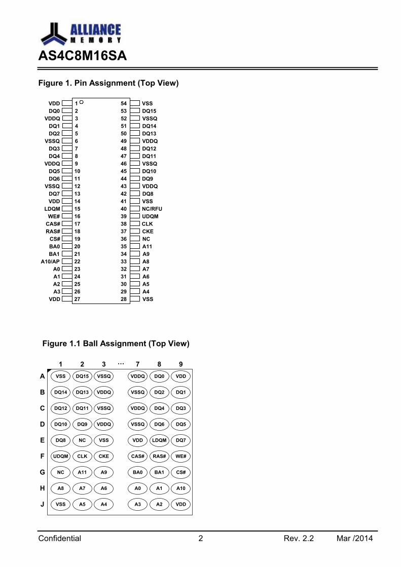
Figure 1. Pin Assignment (Top View)
1 54VDD VSS
2 53DQ0 DQ15
3 52VDDQ VSSQ
4 51DQ1 DQ14
5 50DQ2 DQ13
6 49VSSQ VDDQ
7 48DQ3 DQ12
8 47DQ4 DQ11
9 46VDDQ VSSQ
10 45DQ5 DQ10
11 44DQ6 DQ9
12 43VSSQ VDDQ
13 42DQ7 DQ8
14 41VDD VSS
15 40LDQM NC/RFU
16 39WE# UDQM
17 38CAS# CLK
18 37RAS# CKE
19 36CS# NC
20 35BA0 A11
21 34BA1 A9
22 33A10/AP A8
23 32A0 A7
24 31A1 A6
25 30A2 A5
26 29A3 A4
27 28VDD VSS
Figure 1.1 Ball Assignment (Top View)
… 1 2 7 8
A
B
C
D
E
F
G
H
J
3
VSS DQ15
DQ14 DQ13
DQ12 DQ11
DQ10 DQ9
DQ8 NC
UDQM CLK
NC A11
A8 A7
VSS A5
VSSQ
VDDQ
VSSQ
VDDQ
VSS
CKE
A9
A6
A4
VDDQ DQ0
VSSQ DQ2
VDDQ DQ4
VSSQ DQ6
VDD LDQM
CAS# RAS#
BA0 BA1
A0 A1
A3 A2
VDD
DQ1
DQ3
DQ5
DQ7
WE#
CS#
A10
VDD
9
AS4C8M16SA
Confidential 3 Rev. 2.2 Mar /2014
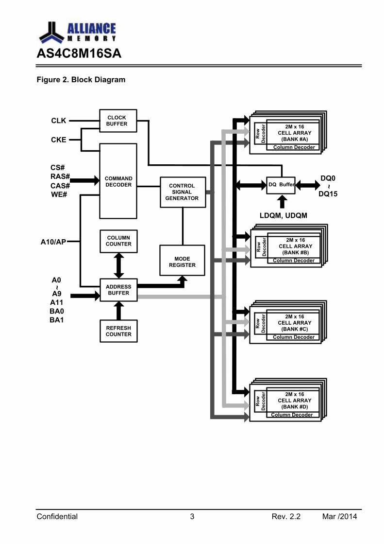
Figure 2. Block Diagram
CLK
CKE
CS#
RAS#
CAS#
WE#
CLOCK
BUFFER
COMMAND
DECODER
COLUMN
COUNTER
CONTROL
SIGNAL
GENERATOR
REFRESH
COUNTER
DQ Buffer
2M x 16
CELL ARRAY
(BANK #A)Ro
w
De
co
de
r
2M x 16
CELL ARRAY
(BANK #B)Ro
w
De
co
de
r
2M x 16
CELL ARRAY
(BANK #C)Ro
w
De
co
de
r
2M x 16
CELL ARRAY
(BANK #D)Ro
w
De
co
de
r
Column Decoder
Column Decoder
Column Decoder
Column Decoder
MODE
REGISTER
A9
A11
BA0
BA1
~
A0
DQ15
DQ0
~
ADDRESS
BUFFER
A10/AP
LDQM, UDQM
AS4C8M16SA
Confidential 4 Rev. 2.2 Mar /2014
Pin Descriptions
Table 3. Pin Details
Symbol Type Description
CLK Input Clock: CLK is driven by the system clock. All SDRAM input signals are sampled on the positive edge of CLK. CLK also increments the internal burst counter and controls the output registers.
CKE Input Clock Enable: CKE activates (HIGH) and deactivates (LOW) the CLK signal. If CKE goes low synchronously with clock (set-up and hold time same as other inputs), the internal clock is suspended from the next clock cycle and the state of output and burst address is frozen as long as the CKE remains low. When all banks are in the idle state, deactivating the clock controls the entry to the Power Down and Self Refresh modes. CKE is synchronous except after the device enters Power Down and Self Refresh modes, where CKE becomes asynchronous until exiting the same mode. The input buffers, including CLK, are disabled during Power Down and Self Refresh modes, providing low standby power.
BA0,BA1 Input Bank Activate: BA0, BA1 input select the bank for operation.
BA1 BA0 Select Bank
0 0 BANK #A
0 1 BANK #B
1 0 BANK #C
1 1 BANK #D
A0-A11 Input Address Inputs: A0-A11 are sampled during the BankActivate command (row address A0-A11) and Read/Write command (column address A0-A8 with A10 defining Auto Precharge) to select one location out of the 2M available in the respective bank. During a Precharge command, A10 is sampled to determine if all banks are to be precharged (A10 = HIGH). The address inputs also provide the op-code during a Mode Register Set command.
CS# Input Chip Select: CS# enables (sampled LOW) and disables (sampled HIGH) the command decoder. All commands are masked when CS# is sampled HIGH. CS# provides for external bank selection on systems with multiple banks. It is considered part of the command code.
RAS# Input Row Address Strobe: The RAS# signal defines the operation commands in conjunction with the CAS# and WE# signals and is latched at the positive edges of CLK. When RAS# and CS# are asserted "LOW" and CAS# is asserted "HIGH," either the BankActivate command or the Precharge command is selected by the WE# signal. When the WE# is asserted "HIGH," the BankActivate command is selected and the bank designated by BA is turned on to the active state. When the WE# is asserted "LOW," the Precharge command is selected and the bank designated by BA is switched to the idle state after the precharge operation.
CAS# Input Column Address Strobe: The CAS# signal defines the operation commands in conjunction with the RAS# and WE# signals and is latched at the positive edges of CLK. When RAS# is held "HIGH" and CS# is asserted "LOW," the column access is started by asserting CAS# "LOW." Then, the Read or Write command is selected by asserting WE# "LOW" or "HIGH."
AS4C8M16SA
Confidential 5 Rev. 2.2 Mar /2014
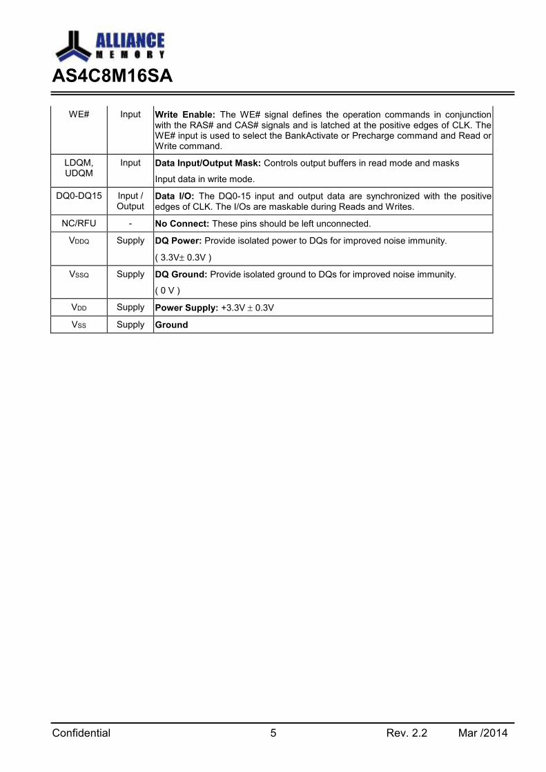
WE# Input Write Enable: The WE# signal defines the operation commands in conjunction with the RAS# and CAS# signals and is latched at the positive edges of CLK. The WE# input is used to select the BankActivate or Precharge command and Read or Write command.
LDQM, UDQM
Input Data Input/Output Mask: Controls output buffers in read mode and masks
Input data in write mode.
DQ0-DQ15 Input / Output
Data I/O: The DQ0-15 input and output data are synchronized with the positive edges of CLK. The I/Os are maskable during Reads and Writes.
NC/RFU - No Connect: These pins should be left unconnected.
VDDQ Supply DQ Power: Provide isolated power to DQs for improved noise immunity.
( 3.3V 0.3V )
VSSQ Supply DQ Ground: Provide isolated ground to DQs for improved noise immunity.
( 0 V )
VDD Supply Power Supply: +3.3V 0.3V
VSS Supply Ground
AS4C8M16SA
Confidential 6 Rev. 2.2 Mar /2014
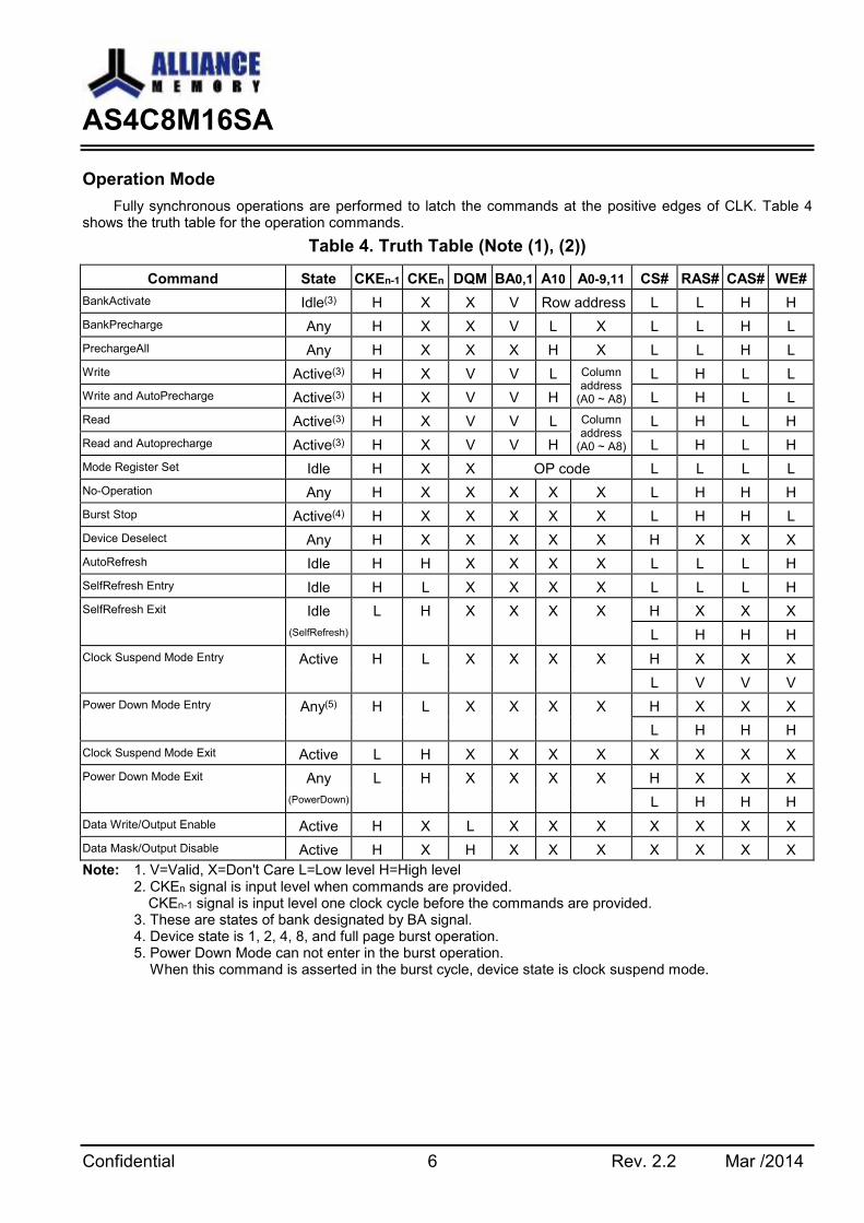
Operation Mode
Fully synchronous operations are performed to latch the commands at the positive edges of CLK. Table 4 shows the truth table for the operation commands.
Table 4. Truth Table (Note (1), (2))
Command State CKEn-1 CKEn DQM BA0,1 A10 A0-9,11 CS# RAS# CAS# WE#
BankActivate Idle(3) H X X V Row address L L H H
BankPrecharge Any H X X V L X L L H L
PrechargeAll Any H X X X H X L L H L
Write Active(3) H X V V L Column address
(A0 ~ A8)
L H L L
Write and AutoPrecharge Active(3) H X V V H L H L L
Read Active(3) H X V V L Column address
(A0 ~ A8)
L H L H
Read and Autoprecharge Active(3) H X V V H L H L H
Mode Register Set Idle H X X OP code L L L L
No-Operation Any H X X X X X L H H H
Burst Stop Active(4) H X X X X X L H H L
Device Deselect Any H X X X X X H X X X
AutoRefresh Idle H H X X X X L L L H
SelfRefresh Entry Idle H L X X X X L L L H
SelfRefresh Exit Idle L H X X X X H X X X
(SelfRefresh) L H H H
Clock Suspend Mode Entry Active H L X X X X H X X X
L V V V
Power Down Mode Entry Any(5) H L X X X X H X X X
L H H H
Clock Suspend Mode Exit Active L H X X X X X X X X
Power Down Mode Exit Any L H X X X X H X X X
(PowerDown) L H H H
Data Write/Output Enable Active H X L X X X X X X X
Data Mask/Output Disable Active H X H X X X X X X X
Note: 1. V=Valid, X=Don't Care L=Low level H=High level 2. CKEn signal is input level when commands are provided.
CKEn-1 signal is input level one clock cycle before the commands are provided. 3. These are states of bank designated by BA signal. 4. Device state is 1, 2, 4, 8, and full page burst operation. 5. Power Down Mode can not enter in the burst operation. When this command is asserted in the burst cycle, device state is clock suspend mode.

AS4C8M16SA
Confidential 7 Rev. 2.2 Mar /2014
Commands
1 BankActivate
(RAS# = "L", CAS# = "H", WE# = "H", BAs = Bank, A0-A11 = Row Address) The BankActivate command activates the idle bank designated by the BA0, 1 signals. By latching
the row address on A0 to A11 at the time of this command, the selected row access is initiated. The read or write operation in the same bank can occur after a time delay of tRCD (min.) from the time of bank activation. A subsequent BankActivate command to a different row in the same bank can only be issued after the previous active row has been precharged (refer to the following figure). The minimum time interval between successive BankActivate commands to the same bank is defined by tRC (min.). The SDRAM has four internal banks on the same chip and shares part of the internal circuitry to reduce chip area; therefore it restricts the back-to-back activation of the two banks. tRRD (min.) specifies the minimum time required between activating different banks. After this command is used, the Write command and the Block Write command perform the no mask write operation.
CLK
COMMAND
T0 T1
ADDRESS
T2 T3 Tn+3 Tn+4 Tn+5 Tn+6
RAS# - CAS# delay(tRCD) RAS# - RAS# delay time(tRRD)
RAS# - Cycle time(tRC)
AutoPrecharge
Begin
Bank A
Row Addr.
Bank A
Col Addr.
Bank B
Row Addr.
Bank A
Row Addr.
Bank A
ActivateNOP NOP
R/W A with
AutoPrecharge
Bank B
ActivateNOP NOP
Bank A
Activate
Don’t Care
Figure 3. BankActivate Command Cycle (Burst Length = n)
2 BankPrecharge command
(RAS# = "L", CAS# = "H", WE# = "L", BAs = Bank, A10 = "L", A0-A9 and A11 = Don't care) The BankPrecharge command precharges the bank designated by BA signal. The precharged bank
is switched from the active state to the idle state. This command can be asserted anytime after tRAS(min.) is satisfied from the BankActivate command in the desired bank. The maximum time any bank can be active is specified by tRAS(max.). Therefore, the precharge function must be performed in any active bank within tRAS(max.). At the end of precharge, the precharged bank is still in the idle state and is ready to be activated again.
3 PrechargeAll command
(RAS# = "L", CAS# = "H", WE# = "L", BAs = Don’t care, A10 = "H", A0-A9 and A11 = Don't care) The PrechargeAll command precharges all banks simultaneously and can be issued even if all banks
are not in the active state. All banks are then switched to the idle state.
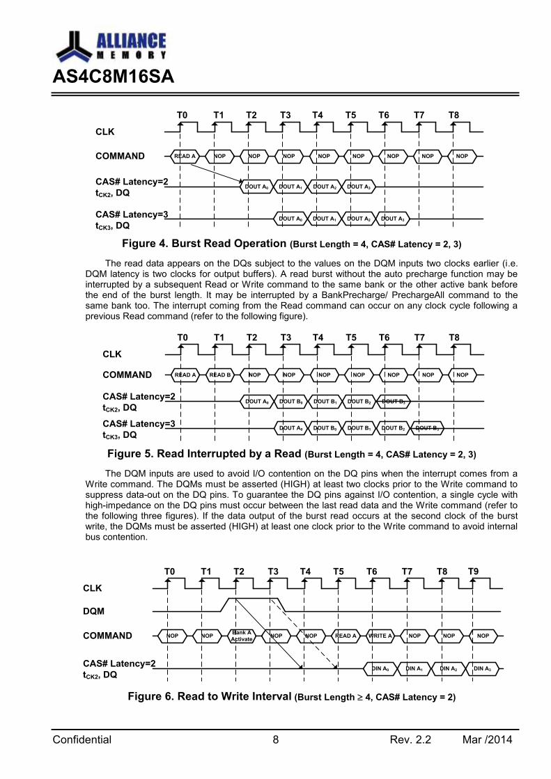
4 Read command
(RAS# = "H", CAS# = "L", WE# = "H", BAs = Bank, A10 = "L", A0-A8 = Column Address) The Read command is used to read a burst of data on consecutive clock cycles from an active row in
an active bank. The bank must be active for at least tRCD (min.) before the Read command is issued. During read bursts, the valid data-out element from the starting column address will be available following the CAS latency after the issue of the Read command. Each subsequent data-out element will be valid by the next positive clock edge (refer to the following figure). The DQs go into high-impedance at the end of the burst unless other command is initiated. The burst length, burst sequence, and CAS latency are determined by the mode register, which is already programmed. A full-page burst will continue until terminated (at the end of the page it will wrap to column 0 and continue).
AS4C8M16SA
Confidential 8 Rev. 2.2 Mar /2014
CLK
COMMAND
T0 T1 T2 T3 T4 T5 T6
READ A NOP NOP NOP NOP NOP NOP NOP
T7 T8
NOP
CAS# Latency=2
tCK2, DQ
CAS# Latency=3
tCK3, DQ
DOUT A0 DOUT A1 DOUT A2 DOUT A3
DOUT A0 DOUT A1 DOUT A2 DOUT A3
Figure 4. Burst Read Operation (Burst Length = 4, CAS# Latency = 2, 3)
The read data appears on the DQs subject to the values on the DQM inputs two clocks earlier (i.e. DQM latency is two clocks for output buffers). A read burst without the auto precharge function may be interrupted by a subsequent Read or Write command to the same bank or the other active bank before the end of the burst length. It may be interrupted by a BankPrecharge/ PrechargeAll command to the same bank too. The interrupt coming from the Read command can occur on any clock cycle following a previous Read command (refer to the following figure).
CLK
COMMAND
T0 T1 T2 T3 T4 T5 T6
READ A READ B NOP NOP NOP NOP NOP NOP
T7 T8
NOP
CAS# Latency=2
tCK2, DQ
CAS# Latency=3
tCK3, DQ
DOUT A0 DOUT B0 DOUT B1 DOUT B2
DOUT A0 DOUT B0 DOUT B1 DOUT B2
DOUT B3
DOUT B3
Figure 5. Read Interrupted by a Read (Burst Length = 4, CAS# Latency = 2, 3)
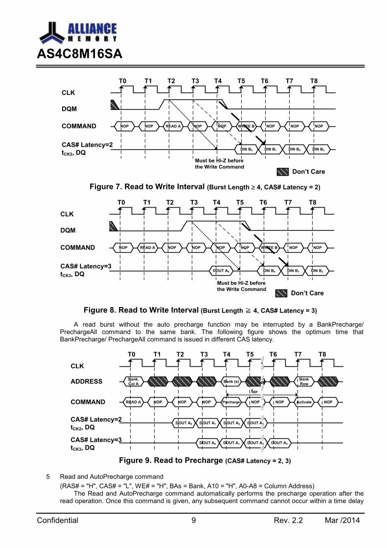
The DQM inputs are used to avoid I/O contention on the DQ pins when the interrupt comes from a Write command. The DQMs must be asserted (HIGH) at least two clocks prior to the Write command to suppress data-out on the DQ pins. To guarantee the DQ pins against I/O contention, a single cycle with high-impedance on the DQ pins must occur between the last read data and the Write command (refer to the following three figures). If the data output of the burst read occurs at the second clock of the burst write, the DQMs must be asserted (HIGH) at least one clock prior to the Write command to avoid internal bus contention.
CLK
COMMAND
T0 T1 T2 T3 T4 T5 T6
NOP NOPBank A
ActivateNOP NOP READ A WRITE A NOP
T7 T8
NOP
CAS# Latency=2
tCK2, DQ
DQM
T9
NOP
DIN A0 DIN A1 DIN A2 DIN A3
Figure 6. Read to Write Interval (Burst Length 4, CAS# Latency = 2)
AS4C8M16SA
Confidential 9 Rev. 2.2 Mar /2014
CLK
COMMAND
T0 T1 T2 T3 T4 T5 T6
NOP NOP READ A NOP NOP WRITE B NOP NOP
T7 T8
NOP
DQM
DIN B0 DIN B1 DIN B2 DIN B3
CAS# Latency=2
tCK2, DQ
Must be Hi-Z before
the Write CommandDon’t Care
Figure 7. Read to Write Interval (Burst Length 4, CAS# Latency = 2)
CLK
COMMAND
T0 T1 T2 T3 T4 T5 T6
NOP READ A NOP NOP NOP NOP WRITE B NOP
T7 T8
NOP
DQM
DOUT A0 DIN B0 DIN B1 DIN B2
CAS# Latency=3
tCK3, DQ
Must be Hi-Z before
the Write CommandDon’t Care
Figure 8. Read to Write Interval (Burst Length ≧ 4, CAS# Latency = 3)
A read burst without the auto precharge function may be interrupted by a BankPrecharge/ PrechargeAll command to the same bank. The following figure shows the optimum time that BankPrecharge/ PrechargeAll command is issued in different CAS latency.
CLK
COMMAND
T0 T1 T2 T3 T4 T5 T6
READ A NOP NOP NOP Precharge NOP NOP Activate
T7 T8
NOP
CAS# Latency=2
tCK2, DQ
CAS# Latency=3
tCK3, DQ
DOUT A0 DOUT A1 DOUT A2 DOUT A3
DOUT A0 DOUT A1 DOUT A2 DOUT A3
ADDRESSBank,
Col ABank (s)
Bank
Row
tRP
Figure 9. Read to Precharge (CAS# Latency = 2, 3)
5 Read and AutoPrecharge command
(RAS# = "H", CAS# = "L", WE# = "H", BAs = Bank, A10 = "H", A0-A8 = Column Address) The Read and AutoPrecharge command automatically performs the precharge operation after the
read operation. Once this command is given, any subsequent command cannot occur within a time delay
AS4C8M16SA
Confidential 10 Rev. 2.2 Mar /2014
of {tRP (min.) + burst length}. At full-page burst, only the read operation is performed in this command and the auto precharge function is ignored.
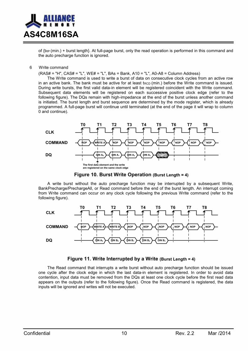
6 Write command
(RAS# = "H", CAS# = "L", WE# = "L", BAs = Bank, A10 = "L", A0-A8 = Column Address) The Write command is used to write a burst of data on consecutive clock cycles from an active row
in an active bank. The bank must be active for at least tRCD (min.) before the Write command is issued. During write bursts, the first valid data-in element will be registered coincident with the Write command. Subsequent data elements will be registered on each successive positive clock edge (refer to the following figure). The DQs remain with high-impedance at the end of the burst unless another command is initiated. The burst length and burst sequence are determined by the mode register, which is already programmed. A full-page burst will continue until terminated (at the end of the page it will wrap to column 0 and continue).
CLK
DQ
T0 T1 T2 T3 T4 T5 T6
DIN A0 DIN A1 DIN A2 DIN A3 don’t care
T7 T8
COMMAND NOP WRITE A NOP NOP NOP NOP NOP NOP NOP
The first data element and the write
are registered on the same clock edge
Figure 10. Burst Write Operation (Burst Length = 4)
A write burst without the auto precharge function may be interrupted by a subsequent Write, BankPrecharge/PrechargeAll, or Read command before the end of the burst length. An interrupt coming from Write command can occur on any clock cycle following the previous Write command (refer to the following figure).
CLK
DQ
T0 T1 T2 T3 T4 T5 T6
DIN A0 DIN B0 DIN B1 DIN B2 DIN B3
T7 T8
COMMAND NOP WRITE A WRITE B NOP NOP NOP NOP NOP NOP
Figure 11. Write Interrupted by a Write (Burst Length = 4)
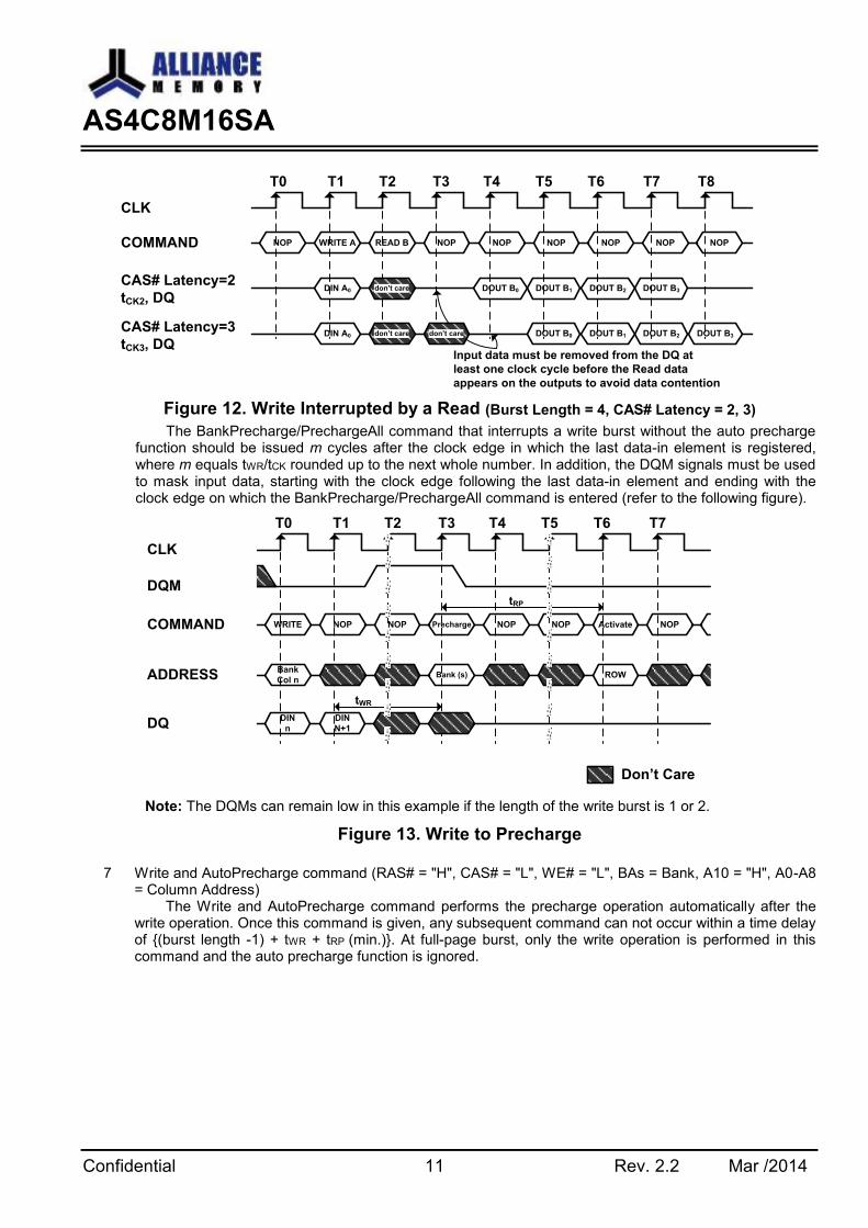
The Read command that interrupts a write burst without auto precharge function should be issued one cycle after the clock edge in which the last data-in element is registered. In order to avoid data contention, input data must be removed from the DQs at least one clock cycle before the first read data appears on the outputs (refer to the following figure). Once the Read command is registered, the data inputs will be ignored and writes will not be executed.
AS4C8M16SA
Confidential 11 Rev. 2.2 Mar /2014
CLK
COMMAND
T0 T1 T2 T3 T4 T5 T6
NOP WRITE A READ B NOP NOP NOP NOP NOP
T7 T8
NOP
CAS# Latency=2
tCK2, DQ
CAS# Latency=3
tCK3, DQ
DOUT B0 DOUT B1 DOUT B2 DOUT B3
DOUT B0 DOUT B1 DOUT B2 DOUT B3
DIN A0 don’t care
DIN A0 don’t care don’t care
Input data must be removed from the DQ at
least one clock cycle before the Read data
appears on the outputs to avoid data contention
Figure 12. Write Interrupted by a Read (Burst Length = 4, CAS# Latency = 2, 3)
The BankPrecharge/PrechargeAll command that interrupts a write burst without the auto precharge function should be issued m cycles after the clock edge in which the last data-in element is registered, where m equals tWR/tCK rounded up to the next whole number. In addition, the DQM signals must be used to mask input data, starting with the clock edge following the last data-in element and ending with the clock edge on which the BankPrecharge/PrechargeAll command is entered (refer to the following figure).
CLK
COMMAND
T0 T1 T2 T3 T4 T5 T6
WRITE NOP NOP Precharge NOP NOP Activate NOP
T7
DQM
Don’t Care
ADDRESSBank
Col nBank (s) ROW
tRP
DIN
n
DIN
N+1
tWR
DQ
Note: The DQMs can remain low in this example if the length of the write burst is 1 or 2.
Figure 13. Write to Precharge
7 Write and AutoPrecharge command (RAS# = "H", CAS# = "L", WE# = "L", BAs = Bank, A10 = "H", A0-A8
= Column Address) The Write and AutoPrecharge command performs the precharge operation automatically after the
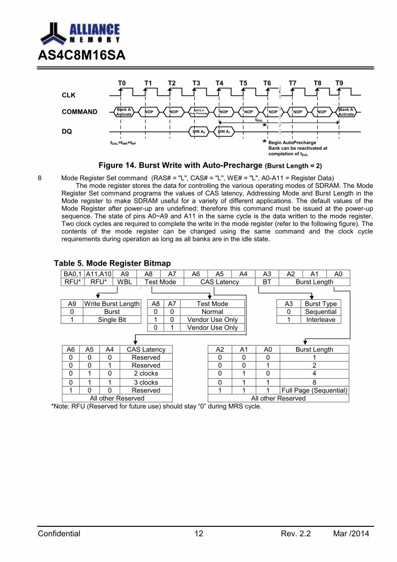
write operation. Once this command is given, any subsequent command can not occur within a time delay of {(burst length -1) + tWR + tRP (min.)}. At full-page burst, only the write operation is performed in this command and the auto precharge function is ignored.
AS4C8M16SA
Confidential 12 Rev. 2.2 Mar /2014
CLK
DQ
T0 T1 T2 T3 T4 T5 T6
DIN A0 DIN A1
T7 T8
COMMANDBank A
ActivateNOP NOP
WRITE A
Auto Precharge NOP NOP NOP NOP NOP
T9
Bank A
Activate
tDAL=tWR+tRP
tDAL
Begin AutoPrecharge
Bank can be reactivated at
completion of tDAL
Figure 14. Burst Write with Auto-Precharge (Burst Length = 2)
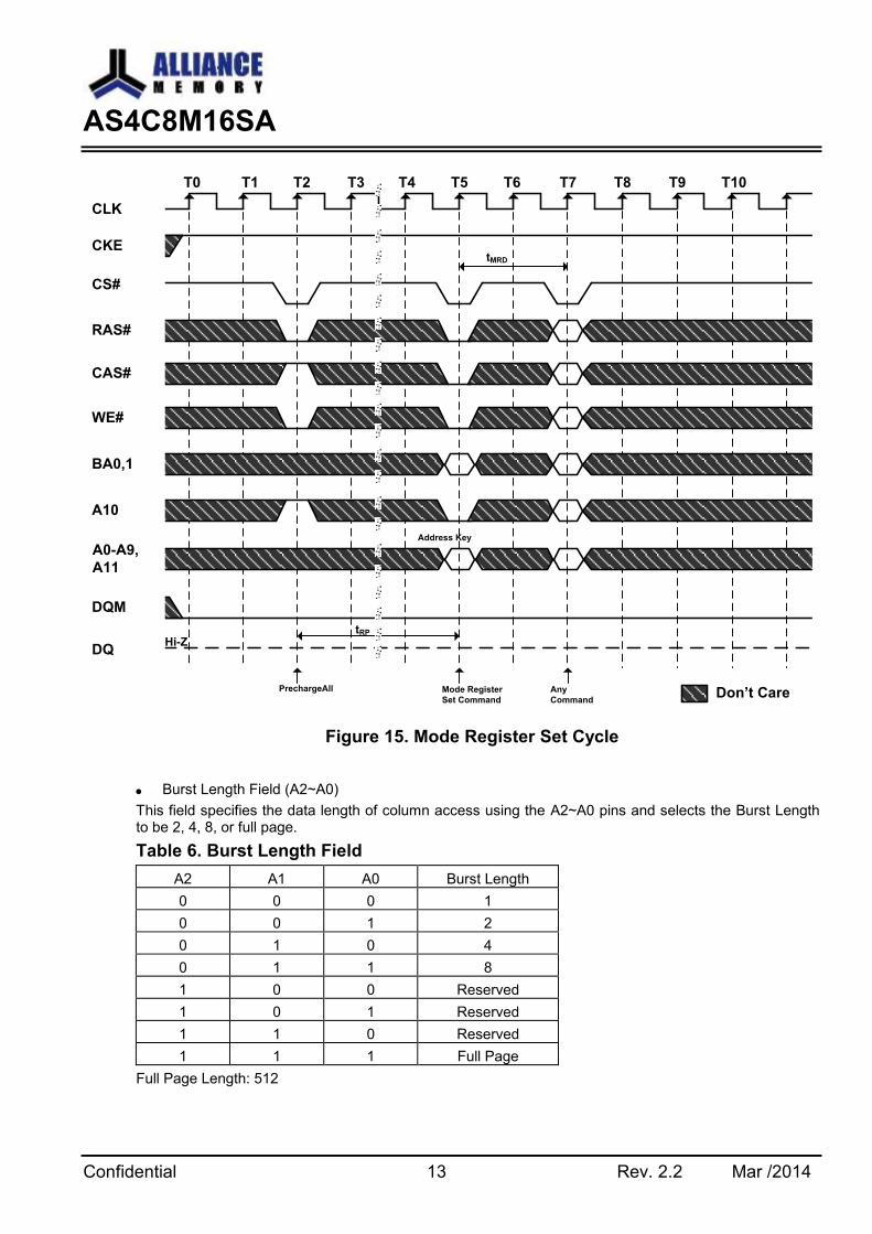
8 Mode Register Set command (RAS# = "L", CAS# = "L", WE# = "L", A0-A11 = Register Data) The mode register stores the data for controlling the various operating modes of SDRAM. The Mode
Register Set command programs the values of CAS latency, Addressing Mode and Burst Length in the Mode register to make SDRAM useful for a variety of different applications. The default values of the Mode Register after power-up are undefined; therefore this command must be issued at the power-up sequence. The state of pins A0~A9 and A11 in the same cycle is the data written to the mode register. Two clock cycles are required to complete the write in the mode register (refer to the following figure). The contents of the mode register can be changed using the same command and the clock cycle requirements during operation as long as all banks are in the idle state.
Table 5. Mode Register Bitmap
BA0,1 A11,A10 A9 A8 A7 A6 A5 A4 A3 A2 A1 A0
RFU* RFU* WBL Test Mode CAS Latency BT Burst Length
A9 Write Burst Length A8 A7 Test Mode A3 Burst Type
0 Burst 0 0 Normal 0 Sequential
1 Single Bit 1 0 Vendor Use Only 1 Interleave
0 1 Vendor Use Only
A6 A5 A4 CAS Latency A2 A1 A0 Burst Length
0 0 0 Reserved 0 0 0 1
0 0 1 Reserved 0 0 1 2
0 1 0 2 clocks 0 1 0 4
0 1 1 3 clocks 0 1 1 8
1 0 0 Reserved 1 1 1 Full Page (Sequential)
All other Reserved All other Reserved
*Note: RFU (Reserved for future use) should stay “0” during MRS cycle.
AS4C8M16SA
Confidential 13 Rev. 2.2 Mar /2014
CLK
CS#
T0 T1 T2 T3 T4 T5 T6 T7
CKE
Don’t Care
RAS#
tMRD
CAS#
T8 T9 T10
WE#
BA0,1
A10
A0-A9,
A11
DQM
DQ
tRP
PrechargeAll Mode Register
Set Command
Any
Command
Hi-Z
Address Key
Figure 15. Mode Register Set Cycle
Burst Length Field (A2~A0)
This field specifies the data length of column access using the A2~A0 pins and selects the Burst Length to be 2, 4, 8, or full page.
Table 6. Burst Length Field
A2 A1 A0 Burst Length
0 0 0 1
0 0 1 2
0 1 0 4
0 1 1 8
1 0 0 Reserved
1 0 1 Reserved
1 1 0 Reserved
1 1 1 Full Page
Full Page Length: 512
AS4C8M16SA
Confidential 14 Rev. 2.2 Mar /2014
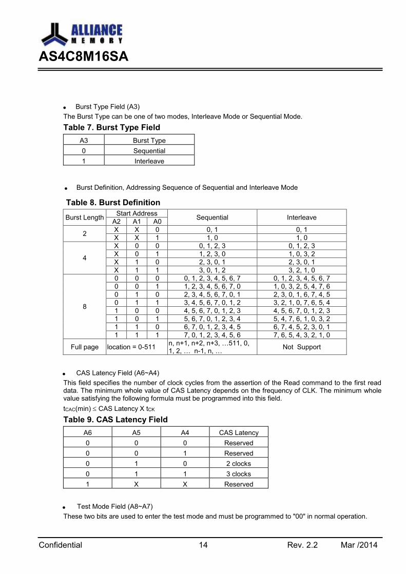
Burst Type Field (A3)
The Burst Type can be one of two modes, Interleave Mode or Sequential Mode.
Table 7. Burst Type Field
A3 Burst Type
0 Sequential
1 Interleave
Burst Definition, Addressing Sequence of Sequential and Interleave Mode
Table 8. Burst Definition
Burst Length Start Address
Sequential Interleave A2 A1 A0
2 X X 0 0, 1 0, 1
X X 1 1, 0 1, 0
4
X 0 0 0, 1, 2, 3 0, 1, 2, 3
X 0 1 1, 2, 3, 0 1, 0, 3, 2
X 1 0 2, 3, 0, 1 2, 3, 0, 1
X 1 1 3, 0, 1, 2 3, 2, 1, 0
8
0 0 0 0, 1, 2, 3, 4, 5, 6, 7 0, 1, 2, 3, 4, 5, 6, 7
0 0 1 1, 2, 3, 4, 5, 6, 7, 0 1, 0, 3, 2, 5, 4, 7, 6
0 1 0 2, 3, 4, 5, 6, 7, 0, 1 2, 3, 0, 1, 6, 7, 4, 5
0 1 1 3, 4, 5, 6, 7, 0, 1, 2 3, 2, 1, 0, 7, 6, 5, 4
1 0 0 4, 5, 6, 7, 0, 1, 2, 3 4, 5, 6, 7, 0, 1, 2, 3
1 0 1 5, 6, 7, 0, 1, 2, 3, 4 5, 4, 7, 6, 1, 0, 3, 2
1 1 0 6, 7, 0, 1, 2, 3, 4, 5 6, 7, 4, 5, 2, 3, 0, 1
1 1 1 7, 0, 1, 2, 3, 4, 5, 6 7, 6, 5, 4, 3, 2, 1, 0
Full page location = 0-511 n, n+1, n+2, n+3, …511, 0, 1, 2, … n-1, n, …
Not Support
CAS Latency Field (A6~A4)
This field specifies the number of clock cycles from the assertion of the Read command to the first read data. The minimum whole value of CAS Latency depends on the frequency of CLK. The minimum whole value satisfying the following formula must be programmed into this field.
tCAC(min) CAS Latency X tCK
Table 9. CAS Latency Field
A6 A5 A4 CAS Latency
0 0 0 Reserved
0 0 1 Reserved
0 1 0 2 clocks
0 1 1 3 clocks
1 X X Reserved
Test Mode Field (A8~A7)
These two bits are used to enter the test mode and must be programmed to "00" in normal operation.
AS4C8M16SA
Confidential 15 Rev. 2.2 Mar /2014
Table 10. Test Mode Field
A8 A7 Test Mode
0 0 normal mode
0 1 Vendor Use Only
1 X Vendor Use Only
Write Burst Length (A9)
This bit is used to select the write burst mode. When the A9 bit is "0", the Burst-Read-Burst-Write
mode is selected. When the A9 bit is "1", the Burst-Read-Single-Write mode is selected.
Table 11. Write Burst Length
A9 Write Burst Mode
0 Burst-Read-Burst-Write
1 Burst-Read-Single-Write
Note: A10 and BA should stay “L” during mode set cycle.
9 No-Operation command
(RAS# = "H", CAS# = "H", WE# = "H")
The No-Operation command is used to perform a NOP to the SDRAM which is selected (CS# is
Low). This prevents unwanted commands from being registered during idle or wait states.
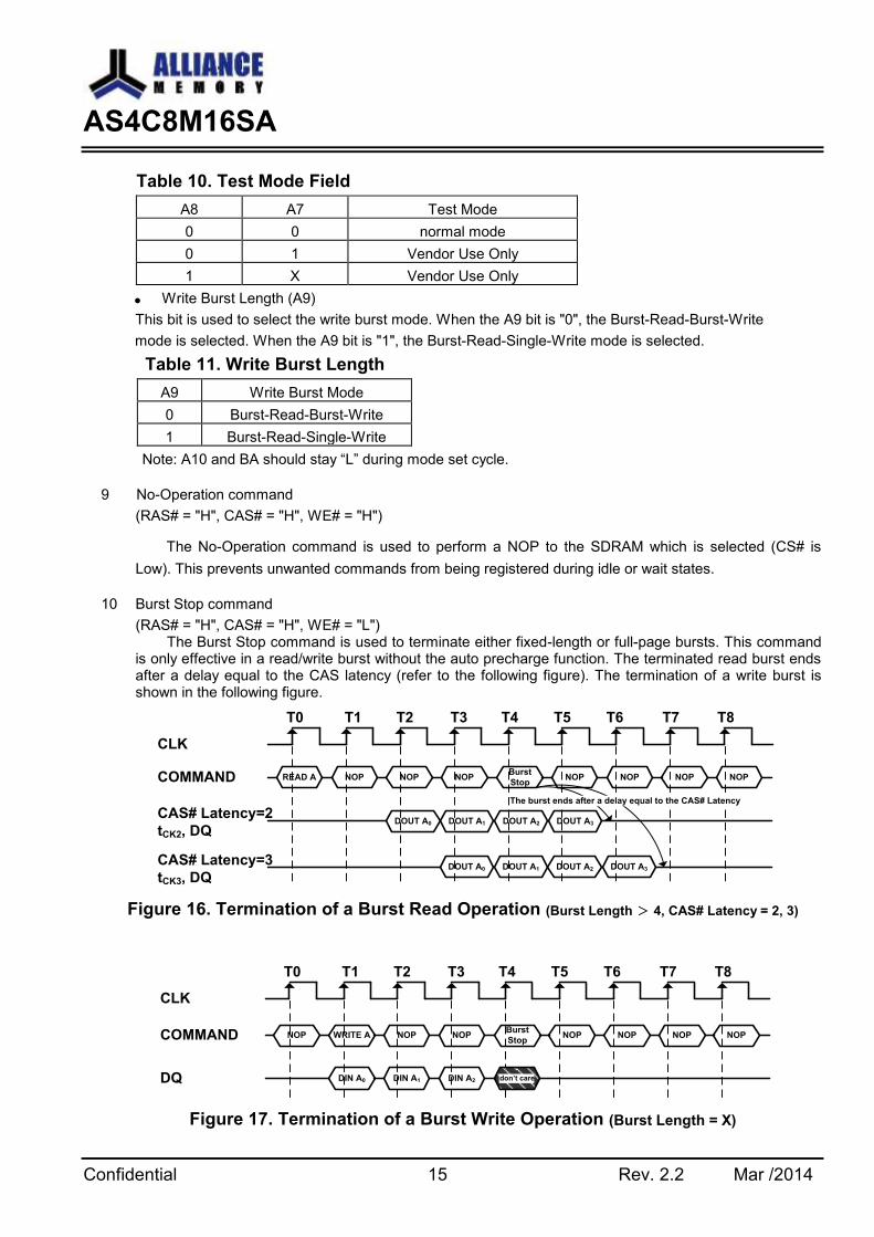
10 Burst Stop command
(RAS# = "H", CAS# = "H", WE# = "L") The Burst Stop command is used to terminate either fixed-length or full-page bursts. This command
is only effective in a read/write burst without the auto precharge function. The terminated read burst ends after a delay equal to the CAS latency (refer to the following figure). The termination of a write burst is shown in the following figure.
CLK
COMMAND
T0 T1 T2 T3 T4 T5 T6
READ A NOP NOP NOPBurst
StopNOP NOP NOP
T7 T8
NOP
CAS# Latency=2
tCK2, DQ
CAS# Latency=3
tCK3, DQ
DOUT A0 DOUT A1 DOUT A2 DOUT A3
DOUT A0 DOUT A1 DOUT A2 DOUT A3
The burst ends after a delay equal to the CAS# Latency
Figure 16. Termination of a Burst Read Operation (Burst Length > 4, CAS# Latency = 2, 3)
CLK
DQ
T0 T1 T2 T3 T4 T5 T6
DIN A0 DIN A1 DIN A2 don’t care
T7 T8
COMMAND NOP WRITE A NOP NOPBurst
StopNOP NOP NOP NOP
Figure 17. Termination of a Burst Write Operation (Burst Length = X)
AS4C8M16SA
Confidential 16 Rev. 2.2 Mar /2014
11 Device Deselect command (CS# = "H")
The Device Deselect command disables the command decoder so that the RAS#, CAS#, WE# and Address inputs are ignored, regardless of whether the CLK is enabled. This command is similar to the No Operation command.
12 AutoRefresh command
(RAS# = "L", CAS# = "L", WE# = "H", CKE = "H", A11 = “Don‘t care, A0-A9 = Don't care) The AutoRefresh command is used during normal operation of the SDRAM and is analogous to
CAS#-before-RAS# (CBR) Refresh in conventional DRAMs. This command is non-persistent, so it must be issued each time a refresh is required. The addressing is generated by the internal refresh controller. This makes the address bits a "don't care" during an AutoRefresh command. The internal refresh counter increments automatically on every auto refresh cycle to all of the rows. The refresh operation must be performed 4096 times within 64ms. The time required to complete the auto refresh operation is specified by tRC(min.). To provide the AutoRefresh command, all banks need to be in the idle state and the device must not be in power down mode (CKE is high in the previous cycle). This command must be followed by NOPs until the auto refresh operation is completed. The precharge time requirement, tRP(min), must be met before successive auto refresh operations are performed.
13 SelfRefresh Entry command
(RAS# = "L", CAS# = "L", WE# = "H", CKE = "L", A0-A9 = Don't care) The SelfRefresh is another refresh mode available in the SDRAM. It is the preferred refresh mode for
data retention and low power operation. Once the SelfRefresh command is registered, all the inputs to the SDRAM become "don't care" with the exception of CKE, which must remain LOW. The refresh addressing and timing is internally generated to reduce power consumption. The SDRAM may remain in SelfRefresh mode for an indefinite period. The SelfRefresh mode is exited by restarting the external clock and then asserting HIGH on CKE (SelfRefresh Exit command).
14 SelfRefresh Exit command
This command is used to exit from the SelfRefresh mode. Once this command is registered, NOP or Device Deselect commands must be issued for tXSR(min.) because time is required for the completion of any bank currently being internally refreshed. If auto refresh cycles in bursts are performed during normal operation, a burst of 4096 auto refresh cycles should be completed just prior to entering and just after exiting the SelfRefresh mode.
15 Clock Suspend Mode Entry / PowerDown Mode Entry command (CKE = "L")
When the SDRAM is operating the burst cycle, the internal CLK is suspended (masked) from the subsequent cycle by issuing this command (asserting CKE "LOW"). The device operation is held intact while CLK is suspended. On the other hand, when all banks are in the idle state, this command performs entry into the PowerDown mode. All input and output buffers (except the CKE buffer) are turned off in the PowerDown mode. The device may not remain in the Clock Suspend or PowerDown state longer than the refresh period (64ms) since the command does not perform any refresh operations.
16 Clock Suspend Mode Exit / PowerDown Mode Exit command (CKE= "H")
When the internal CLK has been suspended, the operation of the internal CLK is reinitiated from the subsequent cycle by providing this command (asserting CKE "HIGH", the command should be NOP or deselect). When the device is in the PowerDown mode, the device exits this mode and all disabled buffers are turned on to the active state. tPDE(min.) is required when the device exits from the PowerDown mode. Any subsequent commands can be issued after one clock cycle from the end of this command.
17 Data Write / Output Enable, Data Mask / Output Disable command (DQM = "L", "H")
During a write cycle, the DQM signal functions as a Data Mask and can control every word of the input data. During a read cycle, the DQM functions as the controller of output buffers. DQM is also used for device selection, byte selection and bus control in a memory system.
AS4C8M16SA
Confidential 17 Rev. 2.2 Mar /2014
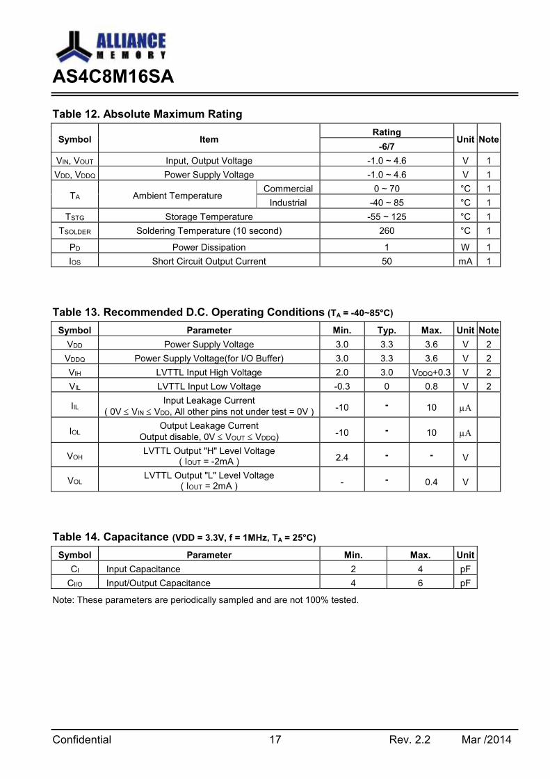
Table 12. Absolute Maximum Rating
Symbol Item Rating
Unit Note -6/7
VIN, VOUT Input, Output Voltage -1.0 ~ 4.6 V 1
VDD, VDDQ Power Supply Voltage -1.0 ~ 4.6 V 1
TA Ambient Temperature Commercial 0 ~ 70 °C 1
Industrial -40 ~ 85 °C 1
TSTG Storage Temperature -55 ~ 125 °C 1
TSOLDER Soldering Temperature (10 second) 260 °C 1
PD Power Dissipation 1 W 1
IOS Short Circuit Output Current 50 mA 1
Table 13. Recommended D.C. Operating Conditions (TA = -40~85°C)
Symbol Parameter Min. Typ. Max. Unit Note
VDD Power Supply Voltage 3.0 3.3 3.6 V 2
VDDQ Power Supply Voltage(for I/O Buffer) 3.0 3.3 3.6 V 2
VIH LVTTL Input High Voltage 2.0 3.0 VDDQ+0.3 V 2
VIL LVTTL Input Low Voltage -0.3 0 0.8 V 2
IIL Input Leakage Current
( 0V VIN VDD, All other pins not under test = 0V ) -10 - 10 A
IOL Output Leakage Current
Output disable, 0V VOUT VDDQ) -10 - 10 A
VOH LVTTL Output "H" Level Voltage
( IOUT = -2mA ) 2.4 - - V
VOL LVTTL Output "L" Level Voltage
( IOUT = 2mA ) - - 0.4 V
Table 14. Capacitance (VDD = 3.3V, f = 1MHz, TA = 25°C)
Symbol Parameter Min. Max. Unit
CI Input Capacitance 2 4 pF
CI/O Input/Output Capacitance 4 6 pF
Note: These parameters are periodically sampled and are not 100% tested.
AS4C8M16SA
Confidential 18 Rev. 2.2 Mar /2014
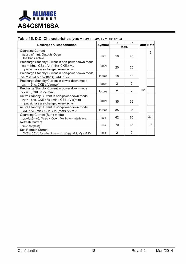
Table 15. D.C. Characteristics (VDD = 3.3V 0.3V, TA = -40~85°C)
Description/Test condition Symbol -6 -7
Unit Note Max.
Operating Current
tRC tRC(min), Outputs Open One bank active
IDD1 50 45
mA
3
Precharge Standby Current in non-power down mode
tCK = 15ns, CS# VIH(min), CKE VIH
Input signals are changed every 2clks
IDD2N 20 20
Precharge Standby Current in non-power down mode
tCK = , CLK VIL(max), CKE VIH IDD2NS 18 18
Precharge Standby Current in power down mode
tCK = 15ns, CKE VIL(max) IDD2P 2 2
Precharge Standby Current in power down mode
tCK = , CKE VIL(max) IDD2PS 2 2
Active Standby Current in non-power down mode
tCK = 15ns, CKE VIH(min), CS# VIH(min) Input signals are changed every 2clks
IDD3N 35 35
Active Standby Current in non-power down mode
CKE VIH(min), CLK VIL(max), tCK = IDD3NS 35 35
Operating Current (Burst mode) tCK =tCK(min), Outputs Open, Multi-bank interleave IDD4 62 60 3, 4
Refresh Current
tRC tRC(min) IDD5 70 65 3
Self Refresh Current CKE 0.2V ; for other inputs VIH VDD - 0.2, VIL 0.2V IDD6 2 2
AS4C8M16SA
Confidential 19 Rev. 2.2 Mar /2014
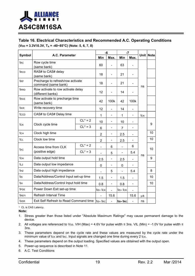
Table 16. Electrical Characteristics and Recommended A.C. Operating Conditions
(VDD = 3.3V±0.3V, TA = -40~85°C) (Note: 5, 6, 7, 8)
Symbol A.C. Parameter -6 -7
Unit Note Min Max. Min Max.
tRC Row cycle time
(same bank) 60 - 63 -
ns
tRCD RAS# to CAS# delay
(same bank) 18 - 21 -
tRP Precharge to refresh/row activate command (same bank) 18 - 21 -
tRRD Row activate to row activate delay
(different banks) 12 - 14 -
tRAS Row activate to precharge time
(same bank) 42 100k 42 100k
tWR Write recovery time 12 - 14 -
tCCD CAS# to CAS# Delay time 1 - 1 - tCK
tCK Clock cycle time
CL* = 2 10 - 10 -
ns
9 CL* = 3 6 - 7 -
tCH Clock high time 2 - 2.5 - 10
tCL Clock low time 2 - 2.5 - 10
tAC Access time from CLK
(positive edge)
CL* = 2 - 6 - 6 10
CL* = 3 - 5 - 5.4
tOH Data output hold time 2.5 - 2.5 - 9
tLZ Data output low impedance 0 - 0 -
tHZ Data output high impedance - 5 - 5.4 8
tIS Data/Address/Control Input set-up time 1.5 - 1.5 - 10
tIH Data/Address/Control Input hold time 0.8 - 0.8 - 10
tPDE Power Down Exit set-up time tIS+ tCK - tIS+ tCK -
tREFI Refresh Interval Time - 15.6 15.6 s
tXSR Exit Self Refresh to Read Command time tIS+ tRC - tIS+ tRC - ns
* CL is CAS Latency.
Note:
1. Stress greater than those listed under "Absolute Maximum Ratings" may cause permanent damage to the device.
2. All voltages are referenced to VSS. VIH (Max) = 4.6V for pulse width ≤ 3ns. VIL (Min) = -1.0V for pulse width ≤ 3ns.
3. These parameters depend on the cycle rate and these values are measured by the cycle rate under the minimum value of tCK and tRC. Input signals are changed one time during every 2 tCK.
4. These parameters depend on the output loading. Specified values are obtained with the output open.
5. Power-up sequence is described in Note 11.
6. A.C. Test Conditions
AS4C8M16SA
Confidential 20 Rev. 2.2 Mar /2014
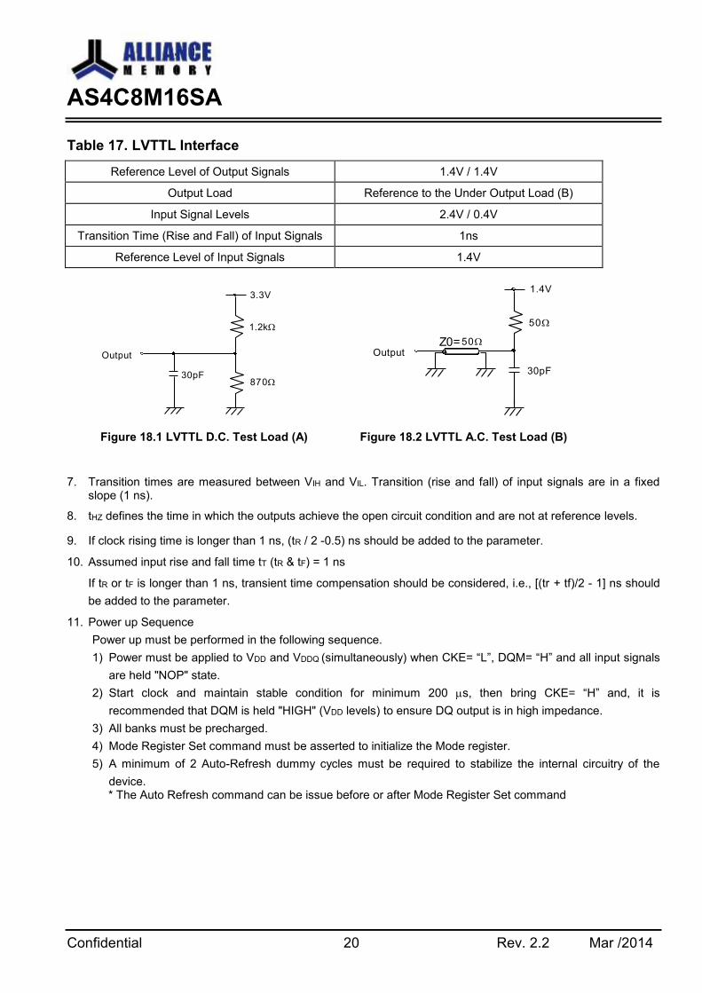
Table 17. LVTTL Interface
Reference Level of Output Signals 1.4V / 1.4V
Output Load Reference to the Under Output Load (B)
Input Signal Levels 2.4V / 0.4V
Transition Time (Rise and Fall) of Input Signals 1ns
Reference Level of Input Signals 1.4V
3.3V
1.2k
87030pF
Output
1.4V
50
Output
30pF
50Z0=
Figure 18.1 LVTTL D.C. Test Load (A) Figure 18.2 LVTTL A.C. Test Load (B)
7. Transition times are measured between VIH and VIL. Transition (rise and fall) of input signals are in a fixed slope (1 ns).
8. tHZ defines the time in which the outputs achieve the open circuit condition and are not at reference levels.
9. If clock rising time is longer than 1 ns, (tR / 2 -0.5) ns should be added to the parameter.
10. Assumed input rise and fall time tT (tR & tF) = 1 ns
If tR or tF is longer than 1 ns, transient time compensation should be considered, i.e., [(tr + tf)/2 - 1] ns should
be added to the parameter.
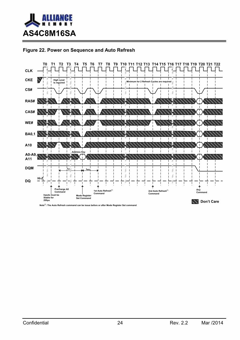
11. Power up Sequence
Power up must be performed in the following sequence.
1) Power must be applied to VDD and VDDQ (simultaneously) when CKE= “L”, DQM= “H” and all input signals
are held "NOP" state.
2) Start clock and maintain stable condition for minimum 200 s, then bring CKE= “H” and, it is
recommended that DQM is held "HIGH" (VDD levels) to ensure DQ output is in high impedance.
3) All banks must be precharged.
4) Mode Register Set command must be asserted to initialize the Mode register.
5) A minimum of 2 Auto-Refresh dummy cycles must be required to stabilize the internal circuitry of the
device. * The Auto Refresh command can be issue before or after Mode Register Set command
AS4C8M16SA
Confidential 21 Rev. 2.2 Mar /2014
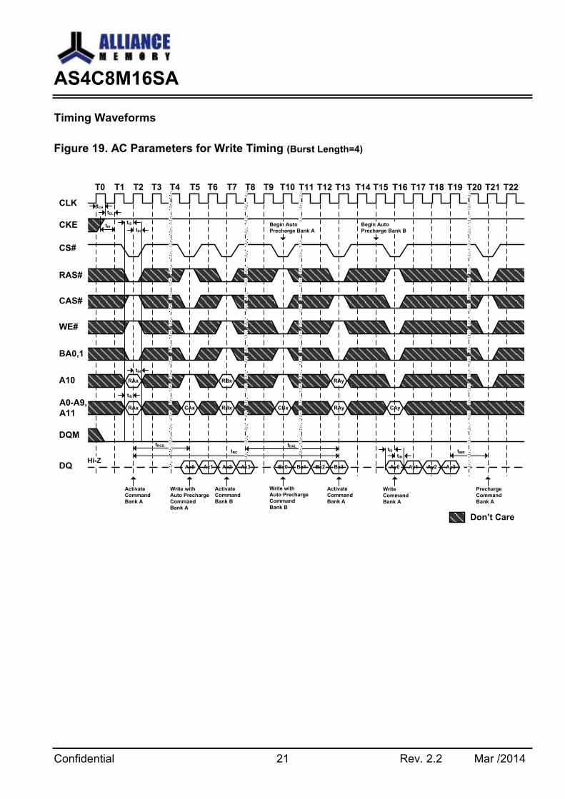
Timing Waveforms
Figure 19. AC Parameters for Write Timing (Burst Length=4)
T0 T1 T2
Don’t Care
tCH
Activate
Command
Bank A
T3 T4 T5 T6 T7 T8 T9 T10 T11 T12 T13 T14 T15 T16 T17 T18 T19 T20 T21 T22
tCL
Begin Auto
Precharge Bank B
RAx RBx RAy
RAx CAx RBx CBx RAy CAy
Ax0 Ax1 Ax2 Ax3 Bx0 Bx1 Bx2 Bx3 Ay0 Ay1 Ay2 Ay3
tRCD
tRC
tDAL
tWR
Write with
Auto Precharge
Command
Bank A
Activate
Command
Bank B
Write with
Auto Precharge
Command
Bank B
Activate
Command
Bank A
Write
Command
Bank A
Precharge
Command
Bank A
tIStIS
tIH
tIH
tIS
Begin Auto
Precharge Bank A
tIS
tIH
Hi-Z
CLK
CS#
CKE
RAS#
CAS#
WE#
BA0,1
A10
A0-A9,
A11
DQM
DQ
AS4C8M16SA
Confidential 22 Rev. 2.2 Mar /2014
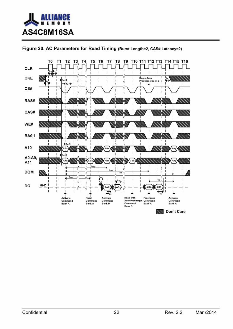
Figure 20. AC Parameters for Read Timing (Burst Length=2, CAS# Latency=2)
Hi-Z
CLK
CS#
T0 T1 T2
CKE
Don’t Care
RAS#
tCH
CAS#
WE#
BA0,1
A10
A0-A9,
A11
DQM
DQ
Activate
Command
Bank A
T3 T4 T5 T6 T7 T8 T9 T10 T11 T12 T13 T14 T15 T16
tCL
Begin Auto
Precharge Bank B
RAx RBx
RAx CAx RBx CBx RAy
RAy
Ax0 Ax1
tRRD
tRC
Read
Command
Bank A
Activate
Command
Bank B
Read with
Auto Precharge
Command
Bank B
Activate
Command
Bank A
tIS
tIH
tIH
tIS
tIS
tIH
tRAS
tRCD tAC
tLZtHZ
Bx0 Bx1
tHZ
tRP
Precharge
Command
Bank A
tOH
AS4C8M16SA
Confidential 23 Rev. 2.2 Mar /2014
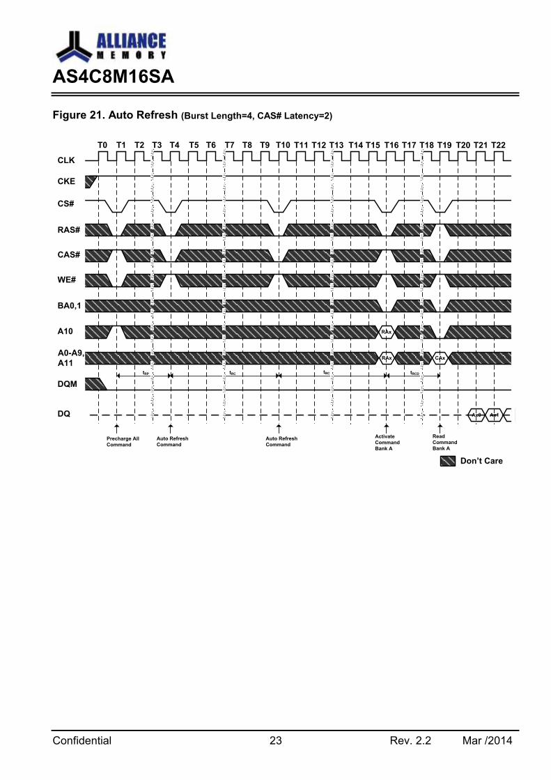
Figure 21. Auto Refresh (Burst Length=4, CAS# Latency=2)
T0 T1 T2
Don’t Care
Precharge All
Command
T3 T4 T5 T6 T7 T8 T9 T10 T11 T12 T13 T14 T15 T16 T17 T18 T19 T20 T21 T22
RAx
CAxRAx
Ax0 Ax1
tRP tRC
Auto Refresh
Command
Auto Refresh
Command
Activate
Command
Bank A
Read
Command
Bank A
tRC tRCD
CLK
CS#
CKE
RAS#
CAS#
WE#
BA0,1
A10
A0-A9,
A11
DQM
DQ
AS4C8M16SA
Confidential 24 Rev. 2.2 Mar /2014
Figure 22. Power on Sequence and Auto Refresh
Hi-Z
T0 T1 T2
Don’t Care
Inputs must be
Stable for
200μs
T3 T4 T5 T6 T7 T8 T9 T10 T11 T12 T13 T14 T15 T16 T17 T18 T19 T20 T21 T22
tMRD
Mode Register
Set Command
High Level
Is reguiredMinimum for 2 Refresh Cycles are required
tRP
Precharge All
Command1st Auto Refresh
(*)
Command2nd Auto Refresh
(*)
Command
Any
Command
Note(*)
: The Auto Refresh command can be issue before or after Mode Register Set command
CLK
CS#
CKE
RAS#
CAS#
WE#
BA0,1
A10
A0-A9,
A11
DQM
DQ
Address Key
AS4C8M16SA
Confidential 25 Rev. 2.2 Mar /2014
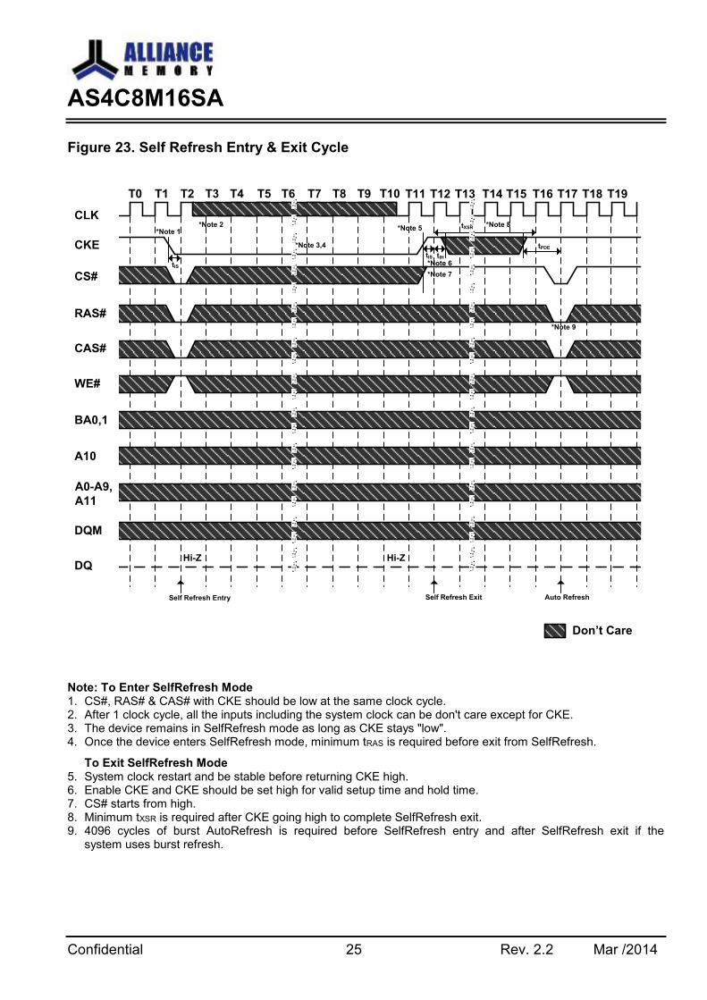
Figure 23. Self Refresh Entry & Exit Cycle
CLK
CS#
T0 T1 T2
CKE
Don’t Care
RAS#
CAS#
WE#
BA0,1
A10
A0-A9,
A11
DQM
DQ
Self Refresh Entry
T3 T4 T5 T6 T7 T8 T9 T10 T11 T12 T13 T14 T15 T16 T17 T18 T19
Self Refresh Exit Auto Refresh
tIS
Hi-Z
tIS tIH
*Note 1*Note 2
*Note 3,4 tPDE
*Note 5
*Note 6
*Note 7
tXSR *Note 8
Hi-Z
*Note 9
Note: To Enter SelfRefresh Mode 1. CS#, RAS# & CAS# with CKE should be low at the same clock cycle. 2. After 1 clock cycle, all the inputs including the system clock can be don't care except for CKE. 3. The device remains in SelfRefresh mode as long as CKE stays "low". 4. Once the device enters SelfRefresh mode, minimum tRAS is required before exit from SelfRefresh.
To Exit SelfRefresh Mode 5. System clock restart and be stable before returning CKE high. 6. Enable CKE and CKE should be set high for valid setup time and hold time. 7. CS# starts from high. 8. Minimum tXSR is required after CKE going high to complete SelfRefresh exit. 9. 4096 cycles of burst AutoRefresh is required before SelfRefresh entry and after SelfRefresh exit if the
system uses burst refresh.

AS4C8M16SA
Confidential 26 Rev. 2.2 Mar /2014
Figure 24.1. Clock Suspension During Burst Read (Using CKE) (Burst Length=4, CAS# Latency=2)
Hi-Z
T0 T1 T2
Don’t Care
T3 T4 T5 T6 T7 T8 T9 T10 T11 T12 T13 T14 T15 T16 T17 T18 T19 T20 T21 T22
RAx
RAx CAx
Activate
Command
Bank A
Read
Command
Bank A
Ax0 Ax1 Ax2 Ax3
tHZ
Clock Suspend
1 CycleClock Suspend
2 Cycles
Clock Suspend
3 Cycles
CLK
CS#
CKE
RAS#
CAS#
WE#
BA0,1
A10
A0-A9,
A11
DQM
DQ
AS4C8M16SA
Confidential 27 Rev. 2.2 Mar /2014
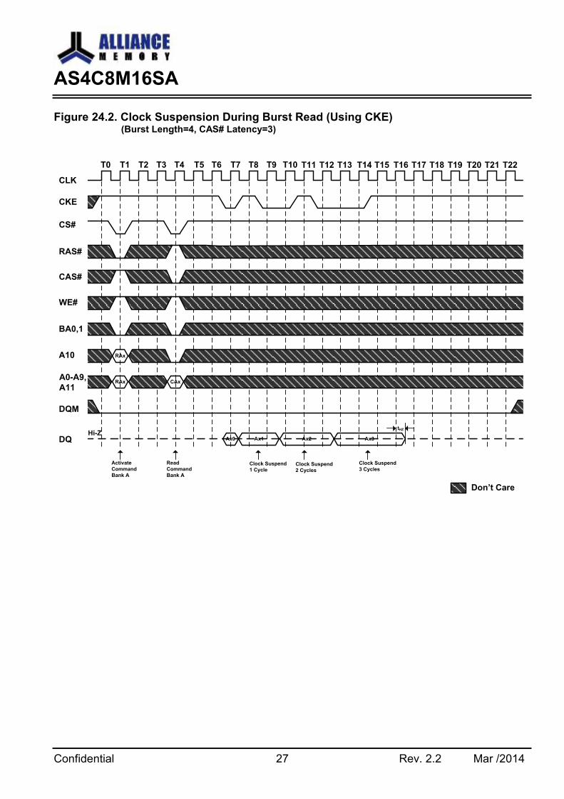
Figure 24.2. Clock Suspension During Burst Read (Using CKE) (Burst Length=4, CAS# Latency=3)
Hi-Z
T0 T1 T2
Don’t Care
T3 T4 T5 T6 T7 T8 T9 T10 T11 T12 T13 T14 T15 T16 T17 T18 T19 T20 T21 T22
RAx
RAx CAx
Activate
Command
Bank A
Read
Command
Bank A
Ax0 Ax1 Ax2 Ax3
tHZ
Clock Suspend
1 CycleClock Suspend
2 Cycles
Clock Suspend
3 Cycles
CLK
CS#
CKE
RAS#
CAS#
WE#
BA0,1
A10
A0-A9,
A11
DQM
DQ
AS4C8M16SA
Confidential 28 Rev. 2.2 Mar /2014
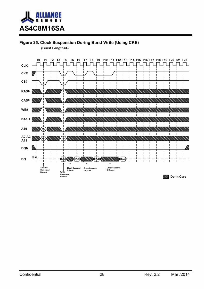
Figure 25. Clock Suspension During Burst Write (Using CKE)
(Burst Length=4)
Hi-Z
T0 T1 T2
Don’t Care
T3 T4 T5 T6 T7 T8 T9 T10 T11 T12 T13 T14 T15 T16 T17 T18 T19 T20 T21 T22
RAx
RAx CAx
Activate
Command
Bank A Write
Command
Bank A
Clock Suspend
1 CycleClock Suspend
2 Cycles
Clock Suspend
3 Cycles
CLK
CS#
CKE
RAS#
CAS#
WE#
BA0,1
A10
A0-A9,
A11
DQM
DQ DAx0 DAx1 DAx2 DAx3
AS4C8M16SA
Confidential 29 Rev. 2.2 Mar /2014
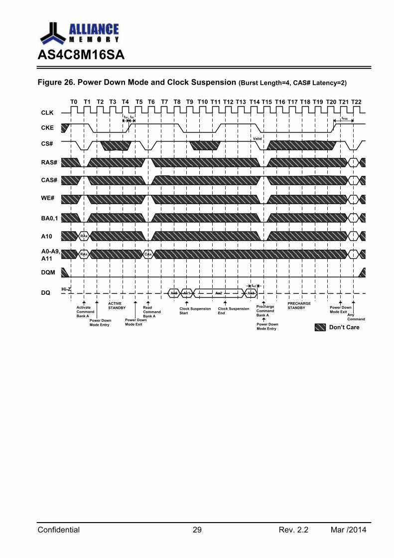
Figure 26. Power Down Mode and Clock Suspension (Burst Length=4, CAS# Latency=2)
Hi-Z
T0 T1 T2
Don’t Care
Activate
Command
Bank A
T3 T4 T5 T6 T7 T8 T9 T10 T11 T12 T13 T14 T15 T16 T17 T18 T19 T20 T21 T22
tIS
Power Down
Mode Exit
tPDE
Power Down
Mode Entry
Read
Command
Bank A
Clock Suspension
Start
Power Down
Mode Exit
tIH
RAx
RAx CAx
Ax0 Ax1 Ax3Ax2
ACTIVE
STANDBY Clock Suspension
End
Precharge
Command
Bank A
Power Down
Mode Entry
PRECHARGE
STANDBY
Any
Command
Valid
tHZ
CLK
CS#
CKE
RAS#
CAS#
WE#
BA0,1
A10
A0-A9,
A11
DQM
DQ

AS4C8M16SA
Confidential 30 Rev. 2.2 Mar /2014
Figure 27.1. Random Column Read (Page within same Bank) (Burst Length=4, CAS# Latency=2)
Hi-Z
T0 T1 T2
Don’t Care
Activate
Command
Bank A
T3 T4 T5 T6 T7 T8 T9 T10 T11 T12 T13 T14 T15 T16 T17 T18 T19 T20 T21 T22
Read
Command
Bank A
RAw
RAw CAx
Aw0 Aw1 Ay2
Precharge
Command
Bank A
CLK
RAz
CAw CAy RAz CAz
Aw2 Aw3 Ax0 Ax1 Ay0 Ay1 Ay3 Az0
Read
Command
Bank A
Read
Command
Bank A
Activate
Command
Bank A
Read
Command
Bank A
CS#
CKE
RAS#
CAS#
WE#
BA0,1
A10
A0-A9,
A11
DQM
DQ
AS4C8M16SA
Confidential 31 Rev. 2.2 Mar /2014
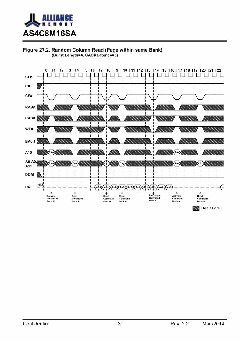
Figure 27.2. Random Column Read (Page within same Bank) (Burst Length=4, CAS# Latency=3)
Hi-Z
T0 T1 T2
Don’t Care
Activate
Command
Bank A
T3 T4 T5 T6 T7 T8 T9 T10 T11 T12 T13 T14 T15 T16 T17 T18 T19 T20 T21 T22
Read
Command
Bank A
RAw
RAw CAx
Aw0 Aw1 Ay2
Precharge
Command
Bank A
CLK
RAz
CAw CAy RAz CAz
Aw2 Aw3 Ax0 Ax1 Ay0 Ay1 Ay3
Read
Command
Bank A
Read
Command
Bank A
Activate
Command
Bank A
Read
Command
Bank A
CS#
CKE
RAS#
CAS#
WE#
BA0,1
A10
A0-A9,
A11
DQM
DQ
AS4C8M16SA
Confidential 32 Rev. 2.2 Mar /2014
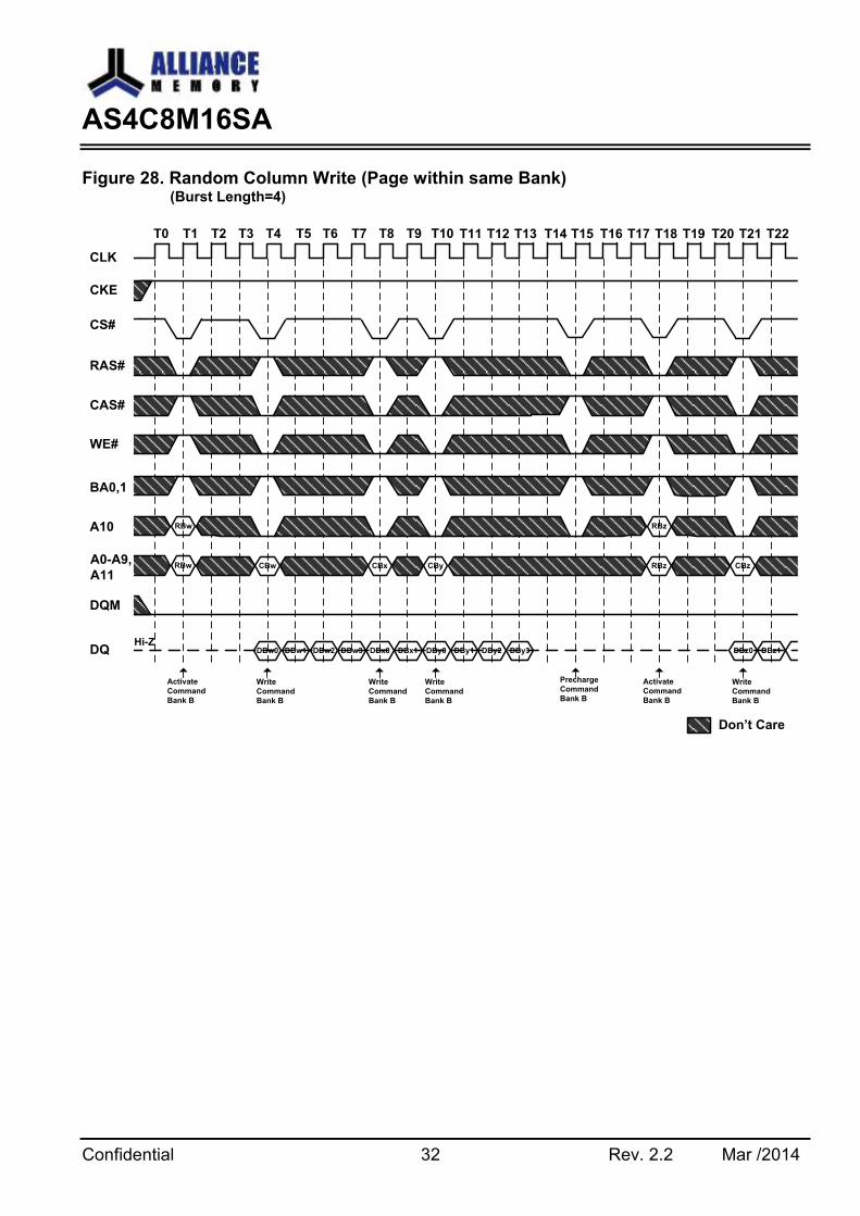
Figure 28. Random Column Write (Page within same Bank) (Burst Length=4)
Hi-Z
T0 T1 T2
Don’t Care
Activate
Command
Bank B
T3 T4 T5 T6 T7 T8 T9 T10 T11 T12 T13 T14 T15 T16 T17 T18 T19 T20 T21 T22
Write
Command
Bank B
RBw
RBw CBx
DBw0 DBw1 DBy2
Precharge
Command
Bank B
CLK
RBz
CBw CBy RBz CBz
DBw2 DBw3 DBx0 DBx1 DBy0 DBy1 DBy3
Write
Command
Bank B
Write
Command
Bank B
Activate
Command
Bank B
Write
Command
Bank B
CS#
CKE
RAS#
CAS#
WE#
BA0,1
A10
A0-A9,
A11
DQM
DQ DBz0 DBz1
AS4C8M16SA
Confidential 33 Rev. 2.2 Mar /2014
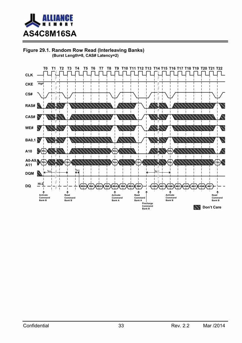
Figure 29.1. Random Row Read (Interleaving Banks) (Burst Length=8, CAS# Latency=2)
Hi-Z
T0 T1 T2
Don’t Care
Activate
Command
Bank B
T3 T4 T5 T6 T7 T8 T9 T10 T11 T12 T13 T14 T15 T16 T17 T18 T19 T20 T21 T22
Read
Command
Bank B
RBx
RBx RAx
Bx0 Bx1 Ax0
Precharge
Command
Bank B
CLK
RBy
CBx CAx RBy CBy
Bx2 Bx3 Bx4 Bx5 Bx6 Bx7 Ax1
Activate
Command
Bank A
Read
Command
Bank A
Activate
Command
Bank B
Read
Command
Bank B
CS#
CKE
WE#
A10
Ax6 Ax7
High
RAx
Ax2 Ax3 Ax4 Ax5
tRCDtAC tRP
A0-A9,
A11
DQM
DQ
BA0,1
RAS#
CAS#
AS4C8M16SA
Confidential 34 Rev. 2.2 Mar /2014
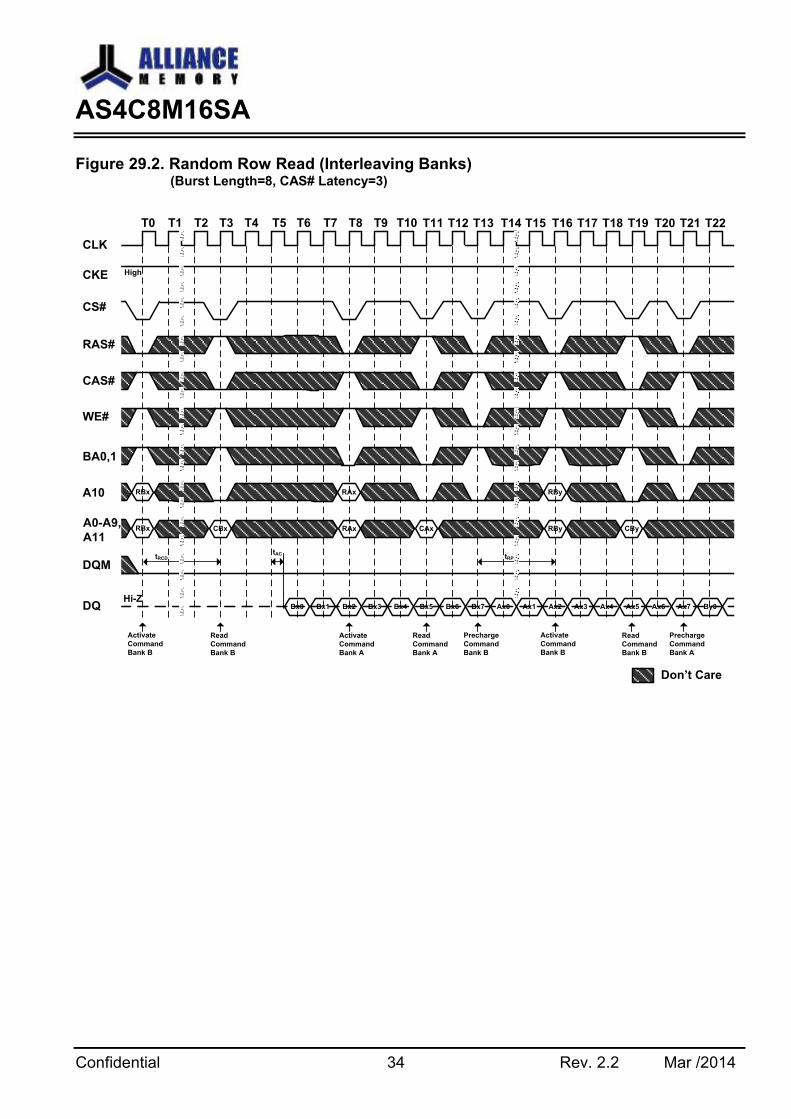
Figure 29.2. Random Row Read (Interleaving Banks) (Burst Length=8, CAS# Latency=3)
Hi-Z
T0 T1 T2
Don’t Care
Activate
Command
Bank B
T3 T4 T5 T6 T7 T8 T9 T10 T11 T12 T13 T14 T15 T16 T17 T18 T19 T20 T21 T22
Read
Command
Bank B
RBx
RBx RAx
Bx0 Bx1 Ax0
Precharge
Command
Bank B
CLK
RBy
CBx CAx RBy CBy
Bx2 Bx3 Bx4 Bx5 Bx6 Bx7 Ax1
Activate
Command
Bank A
Read
Command
Bank A
Activate
Command
Bank B
Read
Command
Bank B
CS#
CKE
WE#
A10
Ax6 Ax7
High
RAx
Ax2 Ax3 Ax4 Ax5
tRCDtAC tRP
A0-A9,
A11
DQM
DQ
BA0,1
RAS#
CAS#
Precharge
Command
Bank A
By0
AS4C8M16SA
Confidential 35 Rev. 2.2 Mar /2014
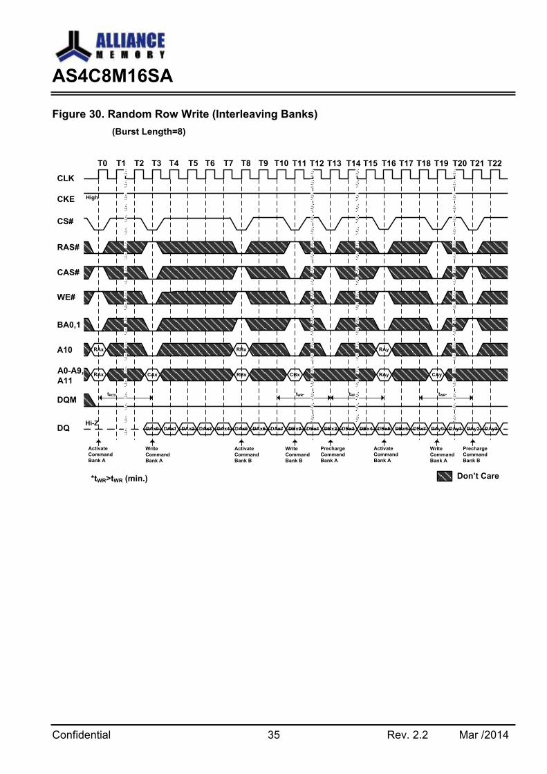
Figure 30. Random Row Write (Interleaving Banks)
(Burst Length=8)
Hi-Z
T0 T1 T2
Don’t Care
Activate
Command
Bank A
T3 T4 T5 T6 T7 T8 T9 T10 T11 T12 T13 T14 T15 T16 T17 T18 T19 T20 T21 T22
Write
Command
Bank A
RAx
RAx RBx
DAx3 DAx4 DBx3
Precharge
Command
Bank A
CLK
RAy
CAx CBx RAy CAy
DAx5 DAx6 DAx7 DBx0 DBx1 DBx2 DBx4
Activate
Command
Bank B
Write
Command
Bank B
Activate
Command
Bank A
Write
Command
Bank A
CS#
CKE
WE#
A10
DAy1 DAy2
High
RBx
DBx5 DBx6 DBx7 DAy0
tRCD tRP
A0-A9,
A11
DQM
DQ
BA0,1
RAS#
CAS#
Precharge
Command
Bank B
DAy3
tWR* tWR*
DAx0 DAx1 DAx2
*tWR>tWR (min.)
AS4C8M16SA
Confidential 36 Rev. 2.2 Mar /2014
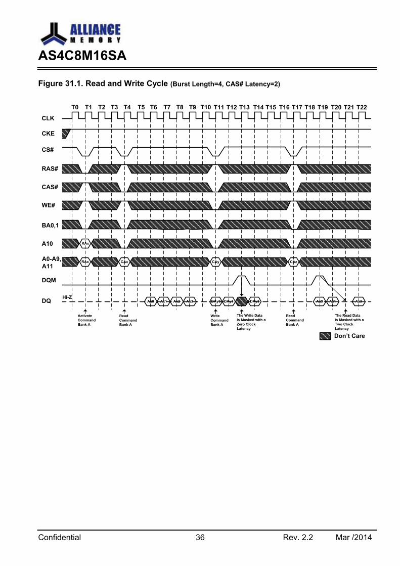
Figure 31.1. Read and Write Cycle (Burst Length=4, CAS# Latency=2)
Hi-Z
T0 T1 T2
Don’t Care
Activate
Command
Bank A
T3 T4 T5 T6 T7 T8 T9 T10 T11 T12 T13 T14 T15 T16 T17 T18 T19 T20 T21 T22
Read
Command
Bank A
RAx
RAx
DAy1
CLK
CAx CAz
Ax0 Ax1 Ax2 Ax3 DAy0
Write
Command
Bank A
The Write Data
is Masked with a
Zero Clock
Latency
Read
Command
Bank A
The Read Data
is Masked with a
Two Clock
Latency
CS#
CKE
RAS#
CAS#
WE#
BA0,1
A10
A0-A9,
A11
DQM
DQ Az1 Az3
CAy
DAy3 Az0
AS4C8M16SA
Confidential 37 Rev. 2.2 Mar /2014
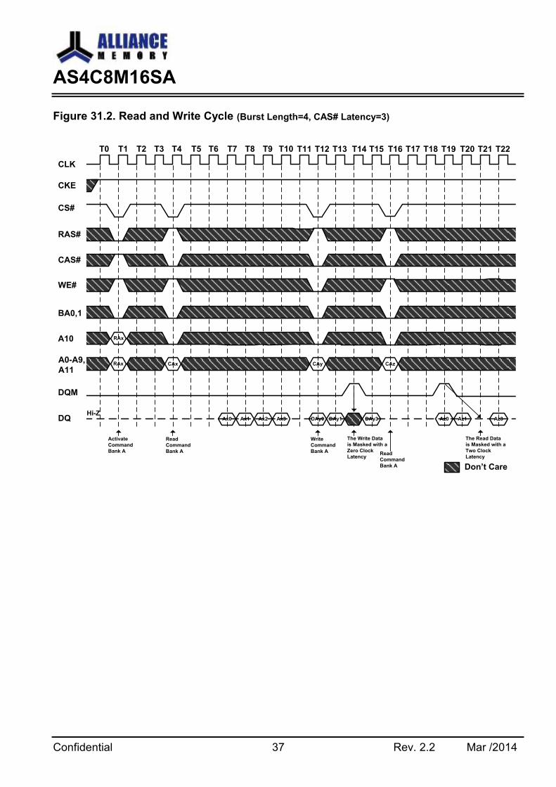
Figure 31.2. Read and Write Cycle (Burst Length=4, CAS# Latency=3)
Hi-Z
T0 T1 T2
Don’t Care
Activate
Command
Bank A
T3 T4 T5 T6 T7 T8 T9 T10 T11 T12 T13 T14 T15 T16 T17 T18 T19 T20 T21 T22
Read
Command
Bank A
RAx
RAx
DAy1
CLK
CAx CAz
Ax0 Ax1 Ax2 Ax3 DAy0
Write
Command
Bank A
The Write Data
is Masked with a
Zero Clock
LatencyRead
Command
Bank A
The Read Data
is Masked with a
Two Clock
Latency
CS#
CKE
RAS#
CAS#
WE#
BA0,1
A10
A0-A9,
A11
DQM
DQ Az1 Az3
CAy
DAy3 Az0
AS4C8M16SA
Confidential 38 Rev. 2.2 Mar /2014
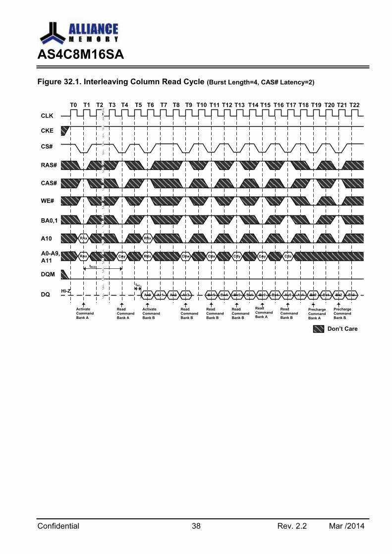
Figure 32.1. Interleaving Column Read Cycle (Burst Length=4, CAS# Latency=2)
Hi-Z
T0 T1 T2
Don’t Care
Activate
Command
Bank A
T3 T4 T5 T6 T7 T8 T9 T10 T11 T12 T13 T14 T15 T16 T17 T18 T19 T20 T21 T22
Read
Command
Bank A
RAx
RAx RBx
Ax0 Ax1 By0
Read
Command
Bank A
CLK
RBx
CAy CBw
Ax2 Ax3 Bw0 Bw1 Bx0 Bx1 By1
Activate
Command
Bank B
Read
Command
Bank B
Read
Command
Bank B
Precharge
Command
Bank B
CS#
CKE
RAS#
CAS#
WE#
BA0,1
A10
A0-A9,
A11
DQM
DQ Bz2 Bz3
CBx CBy CAy CBz
tRCD
tAC
Read
Command
Bank B
Read
Command
Bank B
Bz0Ay0 Ay1 Bz1
Precharge
Command
Bank A
AS4C8M16SA
Confidential 39 Rev. 2.2 Mar /2014
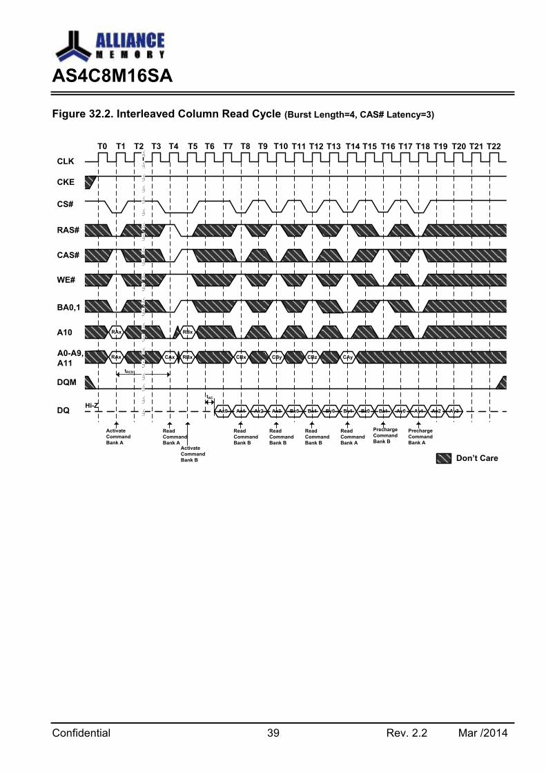
Figure 32.2. Interleaved Column Read Cycle (Burst Length=4, CAS# Latency=3)
Hi-Z
T0 T1 T2
Don’t Care
Activate
Command
Bank A
T3 T4 T5 T6 T7 T8 T9 T10 T11 T12 T13 T14 T15 T16 T17 T18 T19 T20 T21 T22
Read
Command
Bank A
RAx
RAx RBx
Ax0 Ax1 Bz0
Precharge
Command
Bank B
CLK
RBx
CAx CBx
Ax2 Ax3 Bx0 Bx1 By0 By1 Bz1
Activate
Command
Bank B
Read
Command
Bank B
Precharge
Command
Bank A
CS#
CKE
RAS#
CAS#
WE#
BA0,1
A10
A0-A9,
A11
DQM
DQ
CBy CBz CAy
tRCD
tAC
Read
Command
Bank B
Read
Command
Bank A
Ay2Ay0 Ay1 Ay3
Read
Command
Bank B
AS4C8M16SA
Confidential 40 Rev. 2.2 Mar /2014
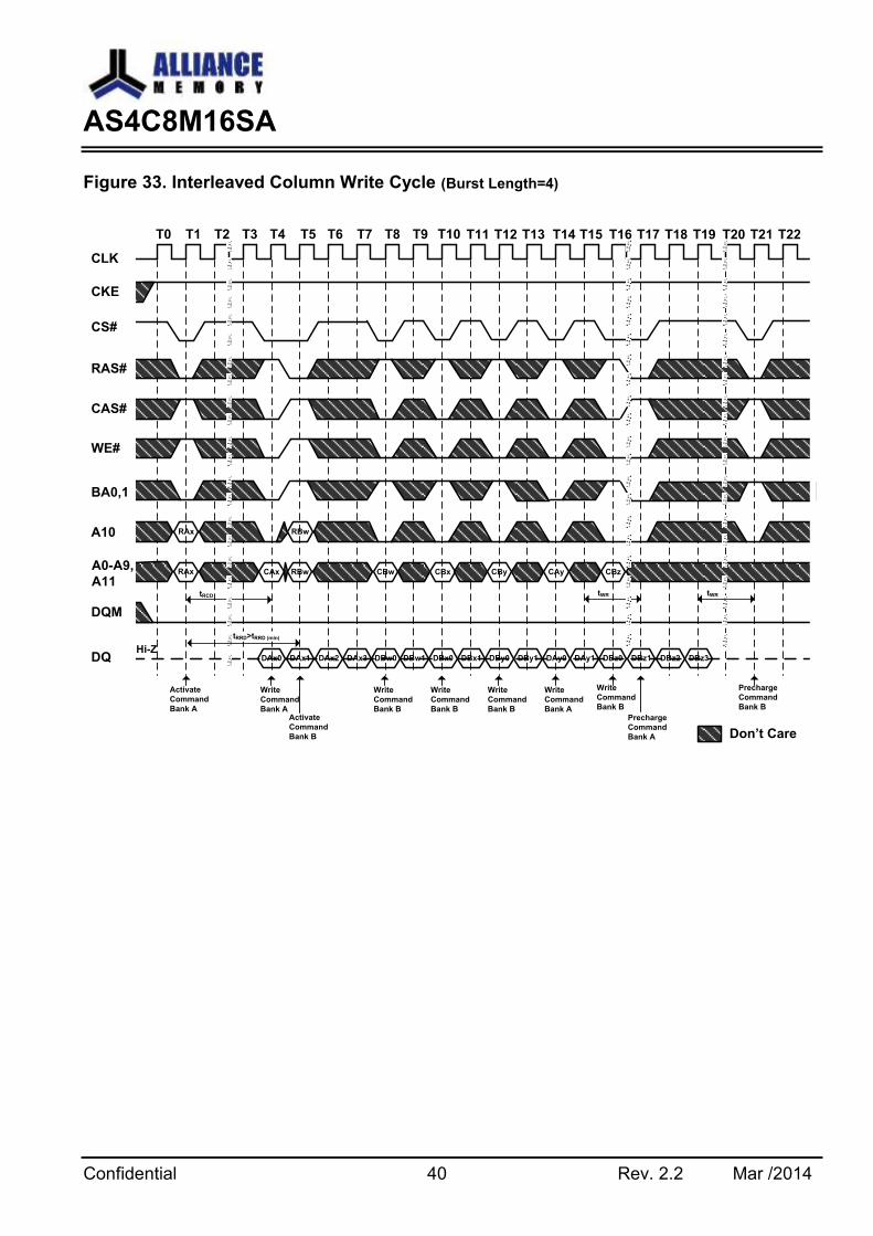
Figure 33. Interleaved Column Write Cycle (Burst Length=4)
Hi-Z
T0 T1 T2
Don’t Care
Activate
Command
Bank A
T3 T4 T5 T6 T7 T8 T9 T10 T11 T12 T13 T14 T15 T16 T17 T18 T19 T20 T21 T22
Write
Command
Bank A
RAx
RAx RBw
DAx0 DAx1 DBy0
Write
Command
Bank B
CLK
RBw
CAx CBw
DAx2 DAx3 DBw0 DBw1 DBx0 DBx1 DBy1
Activate
Command
Bank B
Write
Command
Bank BPrecharge
Command
Bank A
CS#
CKE
RAS#
CAS#
WE#
BA0,1
A10
A0-A9,
A11
DQM
DQ
CBx CBy CAy
tRCD
Write
Command
Bank B
Write
Command
Bank A
DBz0DAy0 DAy1 DBz1
Write
Command
Bank B
CBz
tRRD>tRRD (min)
tWR tWR
DBz2 DBz3
Precharge
Command
Bank B

AS4C8M16SA
Confidential 41 Rev. 2.2 Mar /2014
Figure 34.1. Auto Precharge after Read Burst (Burst Length=4, CAS# Latency=2)
Hi-Z
T0 T1 T2
Don’t Care
Activate
Command
Bank A
T3 T4 T5 T6 T7 T8 T9 T10 T11 T12 T13 T14 T15 T16 T17 T18 T19 T20 T21 T22
Read
Command
Bank A
RAx
RAx CBx
Ax0 Ax1 Bx0
Read with
Auto precharge
Command
Bank A
CLK
RAz
CAx CAy RBy CBy
Ax2 Ax3 Bx1
Activate
Command
Bank B
Read with
Auto Precharge
Command
Bank B
Activate
Command
Bank B
Activate
Command
Bank A
CS#
CKE
WE#
A10
Ay2 Ay3
High
RBx
Bx2 Bx3 Ay0 Ay1
tRP
A0-A9,
A11
DQM
DQ
BA0,1
RAS#
CAS#
RBy
RBx RAz
By2By0 By1
Read with
Auto Precharge
Command
Bank B
Begin Auto
Precharge
Bank B
Begin Auto
Precharge
Bank A
AS4C8M16SA
Confidential 42 Rev. 2.2 Mar /2014
Figure 34.2. Auto Precharge after Read Burst (Burst Length=4, CAS# Latency=3)
Hi-Z
T0 T1 T2
Don’t Care
Activate
Command
Bank A
T3 T4 T5 T6 T7 T8 T9 T10 T11 T12 T13 T14 T15 T16 T17 T18 T19 T20 T21 T22
Read
Command
Bank A
RAx
RAx RBx
Bx2
RBx
CAx CBx
Ax0 Ax1 Ax2 Ax3 Bx0 Bx1 Bx3
Activate
Command
Bank B
Read with
Auto Precharge
Command
Bank A
Read with
Auto Precharge
Command
Bank B
CAy
Activate
Command
Bank B
Ay2Ay0 Ay1 Ay3
Read with
Auto Precharge
Command
Bank B
RBy
tRP
Begin Auto
Precharge
Bank B
Begin Auto
Precharge
Bank A
RBy
CBy
By2By0 By1
CLK
CS#
CKE
RAS#
CAS#
WE#
BA0,1
A10
A0-A9,
A11
DQM
DQ
High
AS4C8M16SA
Confidential 43 Rev. 2.2 Mar /2014
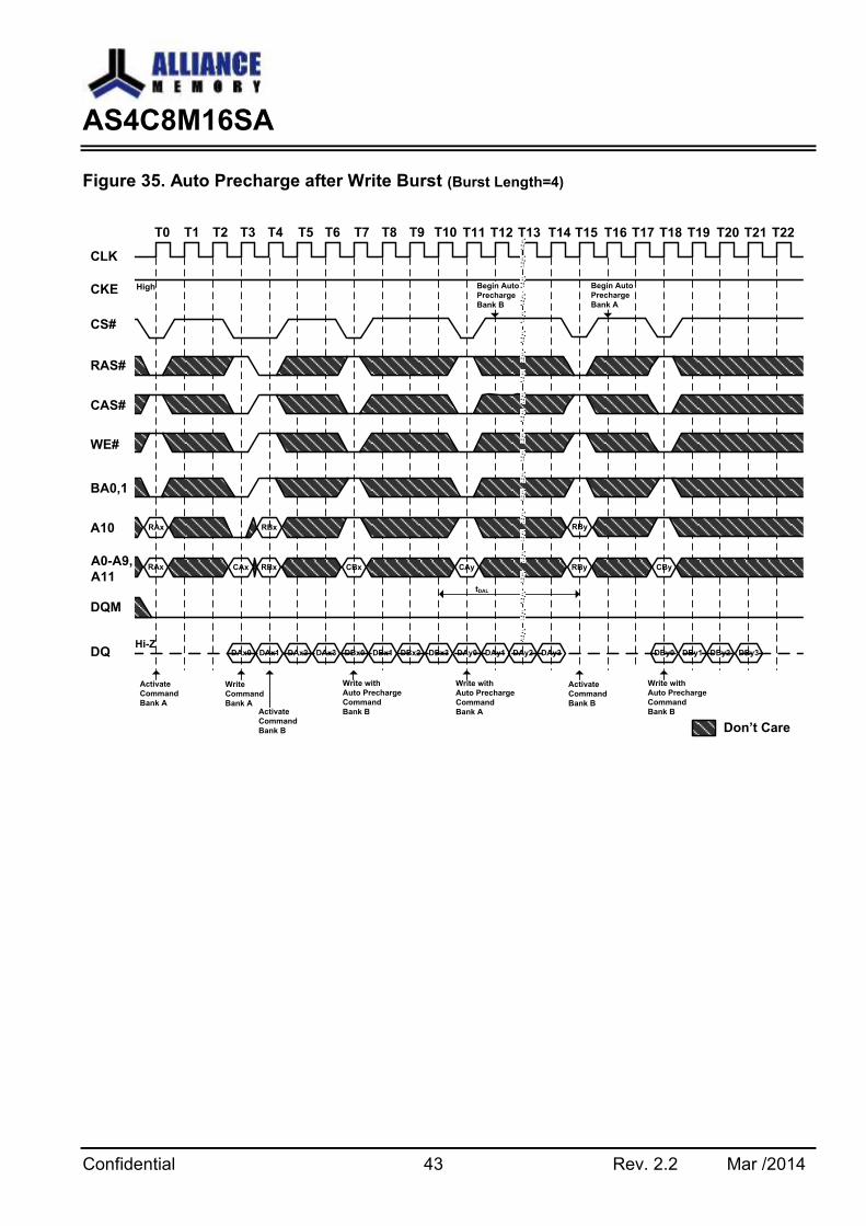
Figure 35. Auto Precharge after Write Burst (Burst Length=4)
Hi-Z
T0 T1 T2
Don’t Care
Activate
Command
Bank A
T3 T4 T5 T6 T7 T8 T9 T10 T11 T12 T13 T14 T15 T16 T17 T18 T19 T20 T21 T22
Write
Command
Bank A
RAx
RAx RBx
DBx2
RBx
CAx CBx
DAx0 DAx1 DAx2 DAx3 DBx0 DBx1 DBx3
Activate
Command
Bank B
Write with
Auto Precharge
Command
Bank A
Write with
Auto Precharge
Command
Bank B
CAy
Activate
Command
Bank B
DAy2DAy0 DAy1 DAy3
Write with
Auto Precharge
Command
Bank B
RBy
tDAL
Begin Auto
Precharge
Bank B
Begin Auto
Precharge
Bank A
RBy
CBy
DBy2DBy0 DBy1
CLK
CS#
CKE
WE#
BA0,1
A10
DQM
DQ
High
DBy3
RAS#
CAS#
A0-A9,
A11

AS4C8M16SA
Confidential 44 Rev. 2.2 Mar /2014
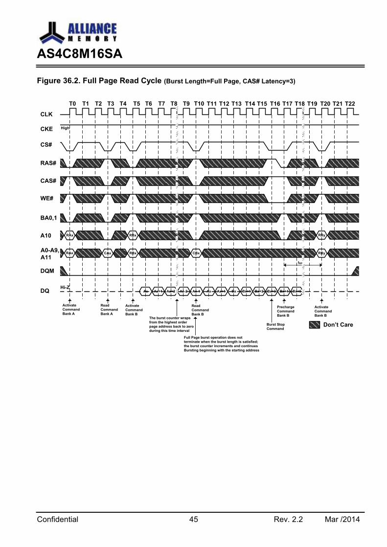
Figure 36.1. Full Page Read Cycle (Burst Length=Full Page, CAS# Latency=2)
Hi-Z
T0 T1 T2
Don’t Care
Activate
Command
Bank A
T3 T4 T5 T6 T7 T8 T9 T10 T11 T12 T13 T14 T15 T16 T17 T18 T19 T20 T21 T22
Read
Command
Bank A
RAx
RAx
Ax+1
RBx
CAx RBx
Ax Ax+1 Ax+2 Ax-2 Ax-1 Ax Bx
Activate
Command
Bank B
Read
Command
Bank B
Precharge
Command
Bank B
CBx
Burst Stop
Command
Bx+3Bx+1 Bx+2 Bx+4
The burst counter wraps
from the highest order
page address back to zero
during this time interval
tRP
RBy
RBy
Bx+5 Bx+6
CLK
CS#
CKE
WE#
A10
DQ
High
Full Page burst operation does not
terminate when the burst length is satisfied;
the burst counter increments and continues
Bursting beginning with the starting address
Activate
Command
Bank B
RAS#
CAS#
BA0,1
A0-A9,
A11
DQM
AS4C8M16SA
Confidential 45 Rev. 2.2 Mar /2014
Figure 36.2. Full Page Read Cycle (Burst Length=Full Page, CAS# Latency=3)
Hi-Z
T0 T1 T2
Don’t Care
Activate
Command
Bank A
T3 T4 T5 T6 T7 T8 T9 T10 T11 T12 T13 T14 T15 T16 T17 T18 T19 T20 T21 T22
Read
Command
Bank A
RAx
RAx
Ax+1
RBx
CAx RBx
Ax Ax+1 Ax+2 Ax-2 Ax-1 Ax Bx
Activate
Command
Bank B
Read
Command
Bank B
Precharge
Command
Bank B
CBx
Burst Stop
Command
Bx+3Bx+1 Bx+2 Bx+4
The burst counter wraps
from the highest order
page address back to zero
during this time interval
tRP
RBy
RBy
Bx+5
CLK
CS#
CKE
WE#
A10
DQ
High
Full Page burst operation does not
terminate when the burst length is satisfied;
the burst counter increments and continues
Bursting beginning with the starting address
Activate
Command
Bank B
RAS#
CAS#
BA0,1
A0-A9,
A11
DQM
AS4C8M16SA
Confidential 46 Rev. 2.2 Mar /2014
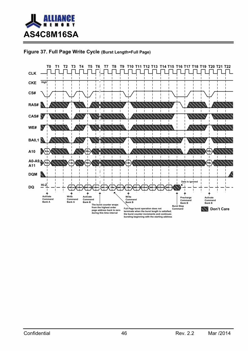
Figure 37. Full Page Write Cycle (Burst Length=Full Page)
Hi-Z
T0 T1 T2
Don’t Care
Activate
Command
Bank A
T3 T4 T5 T6 T7 T8 T9 T10 T11 T12 T13 T14 T15 T16 T17 T18 T19 T20 T21 T22
Write
Command
Bank A
RAx
RAx
DAx+1
RBx
CAx RBx
DAx DAx+1 DAx+2 DAx+3 DAx-1 DAx DBx
Activate
Command
Bank B
Write
Command
Bank B
Precharge
Command
Bank B
CBx
Burst Stop
Command
DBx+3DBx+1 DBx+2 DBx+4
The burst counter wraps
from the highest order
page address back to zero
during this time interval
RBy
RBy
DBx+5
CLK
CS#
CKE
WE#
A10
DQ
High
Full Page burst operation does not
terminate when the burst length is satisfied;
the burst counter increments and continues
bursting beginning with the starting address
Activate
Command
Bank B
RAS#
CAS#
BA0,1
A0-A9,
A11
DQM
Data is ignored
AS4C8M16SA
Confidential 47 Rev. 2.2 Mar /2014
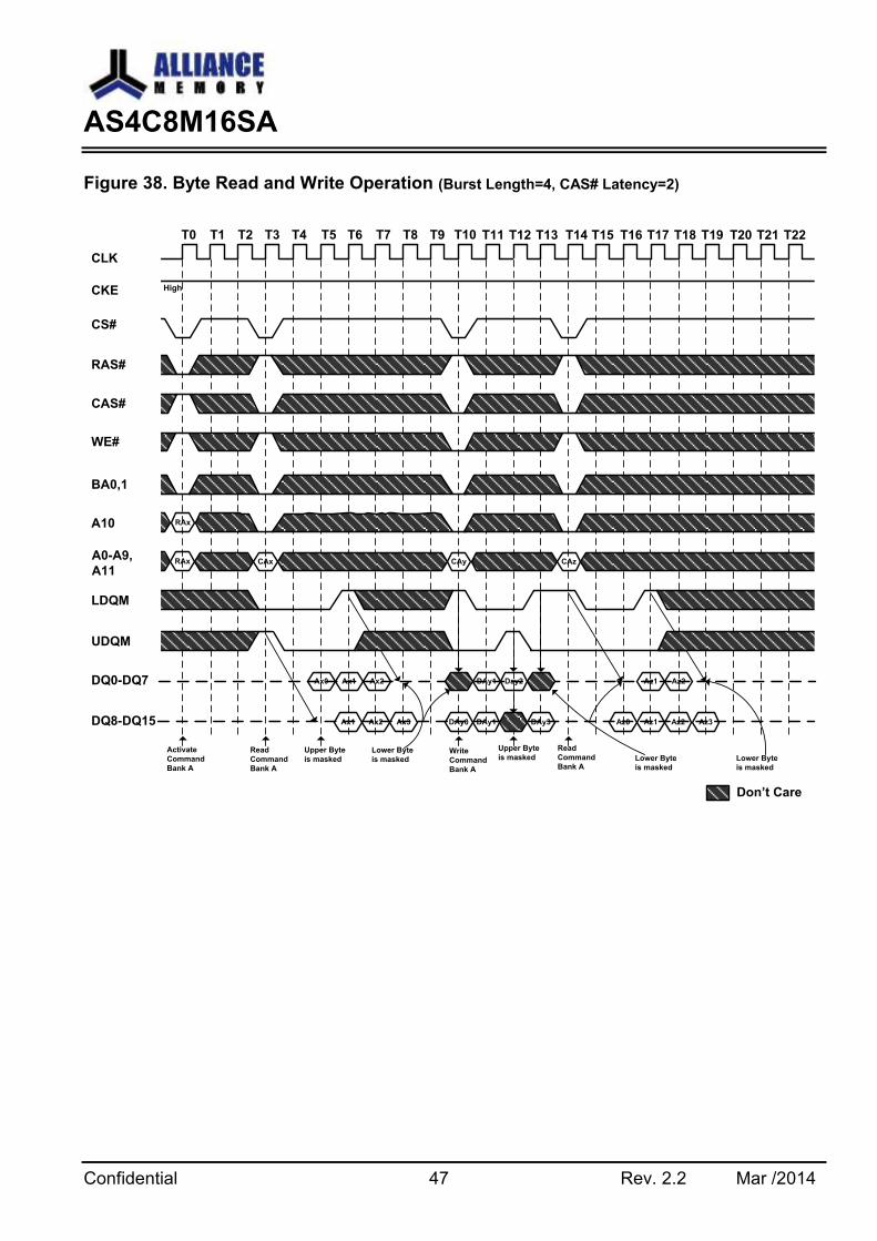
Figure 38. Byte Read and Write Operation (Burst Length=4, CAS# Latency=2)
T0 T1 T2
Don’t Care
Activate
Command
Bank A
T3 T4 T5 T6 T7 T8 T9 T10 T11 T12 T13 T14 T15 T16 T17 T18 T19 T20 T21 T22
Read
Command
Bank A
RAx
RAx CAx
Upper Byte
is maskedWrite
Command
Bank A
Lower Byte
is masked
CAy
Read
Command
Bank A
Lower Byte
is masked
CAz
CLK
CS#
CKE
WE#
A10
DQ8-DQ15
High
Lower Byte
is masked
RAS#
CAS#
BA0,1
A0-A9,
A11
LDQM
UDQM
Ax0 Ax1 Ax2 DAy1 Day2 Az1 Az2DQ0-DQ7
Ax1 Ax2 Ax3 DAy0 DAy3DAy1 Az0 Az1 Az2 Az3
Upper Byte
is masked
AS4C8M16SA
Confidential 48 Rev. 2.2 Mar /2014
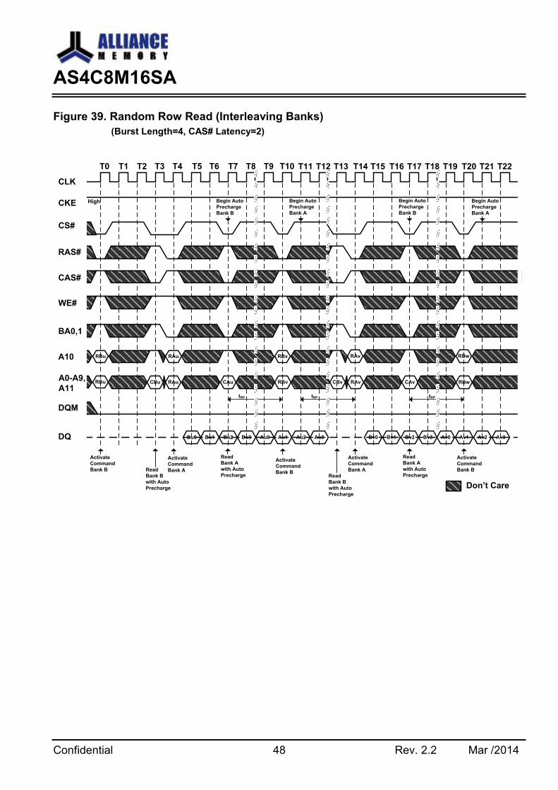
Figure 39. Random Row Read (Interleaving Banks)
(Burst Length=4, CAS# Latency=2)
T0 T1 T2
Don’t Care
Activate
Command
Bank B
T3 T4 T5 T6 T7 T8 T9 T10 T11 T12 T13 T14 T15 T16 T17 T18 T19 T20 T21 T22
Read
Bank B
with Auto
Precharge
RBu
RBu RAu
Bv0
RAu
CBu CAu
Bu0 Bu1 Bu2 Bu3 Au0 Au1 Bv1
Activate
Command
Bank A
Activate
Command
Bank B
Read
Bank A
with Auto
Precharge
RBv
Activate
Command
Bank A
Av0Bv2 Bv3 Av1
Read
Bank A
with Auto
Precharge
CBv
tRP
Begin Auto
Precharge
Bank A
Begin Auto
Precharge
Bank B
RAv
CAv
CLK
CS#
CKE
WE#
A10
DQM
DQ
High Begin Auto
Precharge
Bank B
Begin Auto
Precharge
Bank A
RBw
RBv RAv RBw
tRP tRP
Read
Bank B
with Auto
Precharge
Au2 Au3 Av2 Av3
Activate
Command
Bank B
RAS#
CAS#
BA0,1
A0-A9,
A11
AS4C8M16SA
Confidential 49 Rev. 2.2 Mar /2014
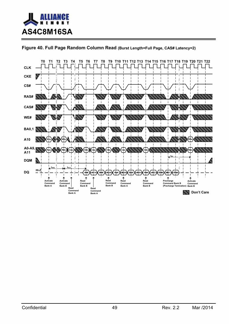
Figure 40. Full Page Random Column Read (Burst Length=Full Page, CAS# Latency=2)
Hi-Z
T0 T1 T2
Don’t Care
Activate
Command
Bank A
T3 T4 T5 T6 T7 T8 T9 T10 T11 T12 T13 T14 T15 T16 T17 T18 T19 T20 T21 T22
Activate
Command
Bank B
RAx
CAx
By1
RBx
RBx CAy
Ax0 Ax1 Bx0 Ay0 Ay1 By0 Az0
Read
Command
Bank A
Read
Command
Bank B
Precharge
Command Bank B
(Precharge Temination)
CAz
Read
Command
Bank A
Bz0Az1 Az2 Bz1
Read
Command
Bank A
CBz
tRP
RBw
RBw
Bz2
CLK
CS#
CKE
RAS#
CAS#
WE#
A10
DQM
DQ
RAx CBx CBy
tRRD tRCD
Read
Command
Bank B
Read
Command
Bank B
Activate
Command
Bank B
BA0,1
A0-A9,
A11
AS4C8M16SA
Confidential 50 Rev. 2.2 Mar /2014
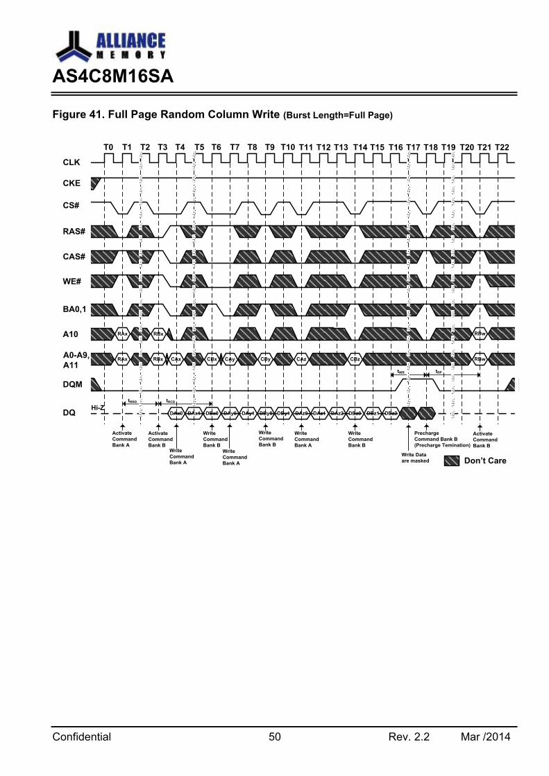
Figure 41. Full Page Random Column Write (Burst Length=Full Page)
Hi-Z
T0 T1 T2
Don’t Care
Activate
Command
Bank A
T3 T4 T5 T6 T7 T8 T9 T10 T11 T12 T13 T14 T15 T16 T17 T18 T19 T20 T21 T22
Activate
Command
Bank B
RAx
CAx
DBy1
RBx
RBx CAy
DAx0 DAx1 DBx0 DAy0 DAy1 DBy0 DAz0
Write
Command
Bank A
Write
Command
Bank B
Precharge
Command Bank B
(Precharge Temination)
CAz
Write
Command
Bank A
DBz0DAz1 DAz2 DBz1
Write
Command
Bank A
CBz
tRP
RBw
RBw
DBz2
CLK
CS#
CKE
RAS#
CAS#
WE#
A10
DQM
DQ
RAx CBx CBy
tRRD tRCD
Write
Command
Bank B
Write
Command
Bank B
Activate
Command
Bank B
BA0,1
A0-A9,
A11tWR
Write Data
are masked
AS4C8M16SA
Confidential 51 Rev. 2.2 Mar /2014
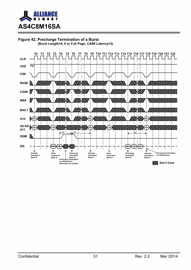
Figure 42. Precharge Termination of a Burst (Burst Length=4, 8 or Full Page, CAS# Latency=3)
T0 T1 T2
Don’t Care
Activate
Command
Bank B
T3 T4 T5 T6 T7 T8 T9 T10 T11 T12 T13 T14 T15 T16 T17 T18 T19 T20 T21 T22
RAx
RAx
Ay0
CAx
DAx0 DAx1 Ay1
Write
Command
Bank A
Activate
Command
Bank A
Activate
Command
Bank A
RAy
Precharge
Command
Bank A
Ay2
Precharge
Command
Bank A
CAy
tWR
RAz
CLK
CS#
CKE
WE#
A10
DQM
DQ
High
RAz
RAy
tRP
Read
Command
Bank A
Precharge Termination
of a Read Burst
tRP
Precharge Termination
of a Write Burst
Write Data are masked
A0-A9,
A11
RAS#
CAS#
BA0,1
AS4C8M16SA
Confidential 52 Rev. 2.2 Mar /2014
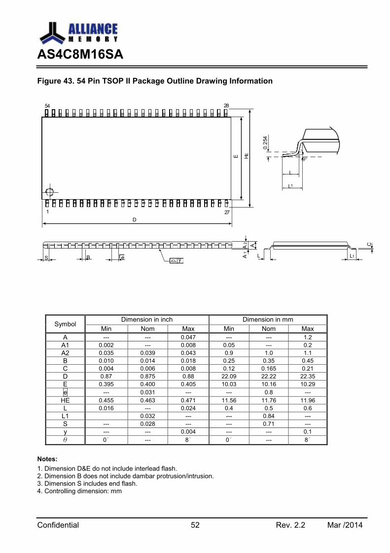
Figure 43. 54 Pin TSOP II Package Outline Drawing Information
yS B eA
A1
A2
L L1
C
54
1
D
E HE
0.2
54
L
L1
27
28
Symbol Dimension in inch Dimension in mm
Min Nom Max Min Nom Max
A --- --- 0.047 --- --- 1.2
A1 0.002 --- 0.008 0.05 --- 0.2
A2 0.035 0.039 0.043 0.9 1.0 1.1
B 0.010 0.014 0.018 0.25 0.35 0.45
C 0.004 0.006 0.008 0.12 0.165 0.21
D 0.87 0.875 0.88 22.09 22.22 22.35
E 0.395 0.400 0.405 10.03 10.16 10.29
e --- 0.031 --- --- 0.8 ---
HE 0.455 0.463 0.471 11.56 11.76 11.96
L 0.016 --- 0.024 0.4 0.5 0.6
L1 0.032 --- --- 0.84 ---
S --- 0.028 --- --- 0.71 ---
y --- --- 0.004 --- --- 0.1
θ 0° --- 8° 0° --- 8°
Notes:
1. Dimension D&E do not include interlead flash. 2. Dimension B does not include dambar protrusion/intrusion. 3. Dimension S includes end flash. 4. Controlling dimension: mm
AS4C8M16SA
Confidential 53 Rev. 2.2 Mar /2014
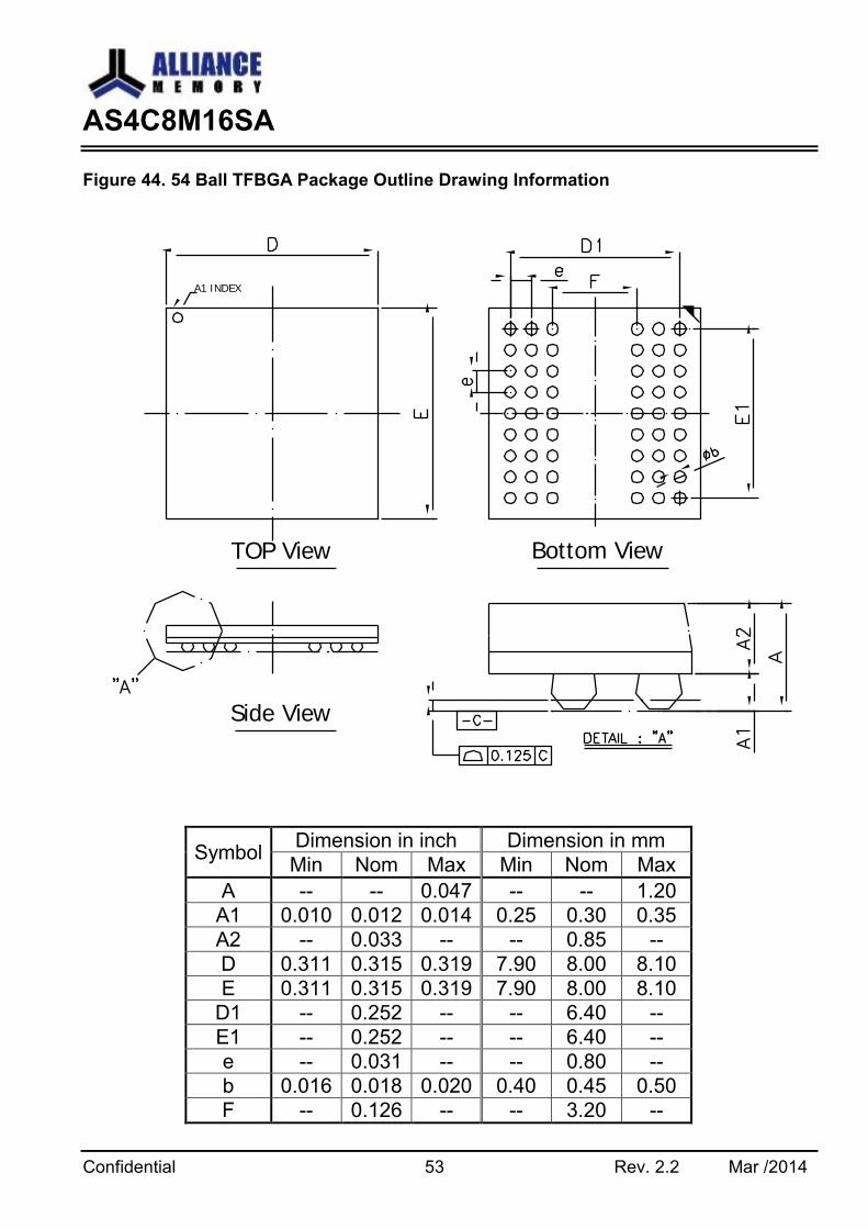
Figure 44. 54 Ball TFBGA Package Outline Drawing Information
TOP View Bottom View
Side View
A1 INDEX
Symbol Dimension in inch Dimension in mm
Min Nom Max Min Nom Max
A -- -- 0.047 -- -- 1.20
A1 0.010 0.012 0.014 0.25 0.30 0.35
A2 -- 0.033 -- -- 0.85 --
D 0.311 0.315 0.319 7.90 8.00 8.10
E 0.311 0.315 0.319 7.90 8.00 8.10
D1 -- 0.252 -- -- 6.40 --
E1 -- 0.252 -- -- 6.40 --
e -- 0.031 -- -- 0.80 --
b 0.016 0.018 0.020 0.40 0.45 0.50
F -- 0.126 -- -- 3.20 --
AS4C8M16SA
Confidential 54 Rev. 2.2 Mar /2014


