12×8 DOTS MATRIX LED DRIVER
12
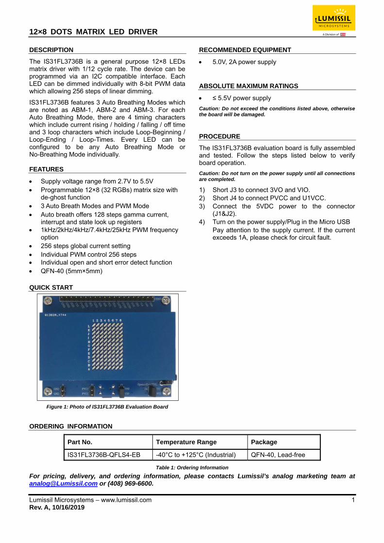
12×8 DOTS MATRIX LED DRIVER Lumissil Microsystems – www.lumissil.com 1 Rev. A, 10/16/2019 DESCRIPTION The IS31FL3736B is a general purpose 12×8 LEDs matrix driver with 1/12 cycle rate. The device can be programmed via an I2C compatible interface. Each LED can be dimmed individually with 8-bit PWM data which allowing 256 steps of linear dimming. IS31FL3736B features 3 Auto Breathing Modes which are noted as ABM-1, ABM-2 and ABM-3. For each Auto Breathing Mode, there are 4 timing characters which include current rising / holding / falling / off time and 3 loop characters which include Loop-Beginning / Loop-Ending / Loop-Times. Every LED can be configured to be any Auto Breathing Mode or No-Breathing Mode individually. FEATURES Supply voltage range from 2.7V to 5.5V Programmable 12×8 (32 RGBs) matrix size with de-ghost function 3 Auto Breath Modes and PWM Mode Auto breath offers 128 steps gamma current, interrupt and state look up registers 1kHz/2kHz/4kHz/7.4kHz/25kHz PWM frequency option 256 steps global current setting Individual PWM control 256 steps Individual open and short error detect function QFN-40 (5mm×5mm) QUICK START Figure 1: Photo of IS31FL3736B Evaluation Board RECOMMENDED EQUIPMENT 5.0V, 2A power supply ABSOLUTE MAXIMUM RATINGS ≤ 5.5V power supply Caution: Do not exceed the conditions listed above, otherwise the board will be damaged. PROCEDURE The IS31FL3736B evaluation board is fully assembled and tested. Follow the steps listed below to verify board operation. Caution: Do not turn on the power supply until all connections are completed. 1) Short J3 to connect 3VO and VIO. 2) Short J4 to connect PVCC and U1VCC. 3) Connect the 5VDC power to the connector (J1&J2). 4) Turn on the power supply/Plug in the Micro USB Pay attention to the supply current. If the current exceeds 1A, please check for circuit fault. ORDERING INFORMATION Part No. Temperature Range Package IS31FL3736B-QFLS4-EB -40°C to +125°C (Industrial) QFN-40, Lead-free Table 1: Ordering Information For pricing, delivery, and ordering information, please contacts Lumissil’s analog marketing team at [email protected] or (408) 969-6600.
Transcript of 12×8 DOTS MATRIX LED DRIVER
12×8 DOTS MATRIX LED DRIVER
Lumissil Microsystems – www.lumissil.com 1 Rev. A, 10/16/2019
DESCRIPTION
The IS31FL3736B is a general purpose 12×8 LEDs matrix driver with 1/12 cycle rate. The device can be programmed via an I2C compatible interface. Each LED can be dimmed individually with 8-bit PWM data which allowing 256 steps of linear dimming.
IS31FL3736B features 3 Auto Breathing Modes which are noted as ABM-1, ABM-2 and ABM-3. For each Auto Breathing Mode, there are 4 timing characters which include current rising / holding / falling / off time and 3 loop characters which include Loop-Beginning / Loop-Ending / Loop-Times. Every LED can be configured to be any Auto Breathing Mode or No-Breathing Mode individually. FEATURES
Supply voltage range from 2.7V to 5.5V Programmable 12×8 (32 RGBs) matrix size with
de-ghost function 3 Auto Breath Modes and PWM Mode Auto breath offers 128 steps gamma current,
interrupt and state look up registers 1kHz/2kHz/4kHz/7.4kHz/25kHz PWM frequency
option 256 steps global current setting Individual PWM control 256 steps Individual open and short error detect function QFN-40 (5mm×5mm)
QUICK START
Figure 1: Photo of IS31FL3736B Evaluation Board
RECOMMENDED EQUIPMENT
5.0V, 2A power supply
ABSOLUTE MAXIMUM RATINGS
≤ 5.5V power supply
Caution: Do not exceed the conditions listed above, otherwise the board will be damaged.
PROCEDURE
The IS31FL3736B evaluation board is fully assembled and tested. Follow the steps listed below to verify board operation.
Caution: Do not turn on the power supply until all connections are completed.
1) Short J3 to connect 3VO and VIO. 2) Short J4 to connect PVCC and U1VCC. 3) Connect the 5VDC power to the connector
(J1&J2). 4) Turn on the power supply/Plug in the Micro USB
Pay attention to the supply current. If the current exceeds 1A, please check for circuit fault.
ORDERING INFORMATION
Part No. Temperature Range Package
IS31FL3736B-QFLS4-EB -40°C to +125°C (Industrial) QFN-40, Lead-free
Table 1: Ordering Information
For pricing, delivery, and ordering information, please contacts Lumissil’s analog marketing team at [email protected] or (408) 969-6600.
12×8 DOTS MATRIX LED DRIVER
Lumissil Microsystems – www.lumissil.com 2 Rev. A, 10/16/2019
EVALUATION BOARD OPERATION
The IS31FL3736B evaluation board has three animation display modes. Press K1 to switch configurations.
1) Line-shaded animation 2) Heart animation 3) Dot-shaded line animation 4) All LED turn on
Note: IS31FL3736B solely controls the FxLED function on the evaluation board.
SOFTWARE CONTROL
J4 default setting is closed (short). If it is set to open, the U1 (LDO) will stop working and all the 3V, including the supply of MCU will be cut off, all the MCU's IO will be high impedance (open-drain) and external control is allowed.
The IS31FL3736B can set its I2C bus interface logic threshold based on the voltage on the VIO pin. An external VIO voltage in the range of 1.8V≤VIO≤VCC can be applied after removing (open) the J4 jumper.
The board comes with J4 default setting closed (short). If it is set to open, the user can connect an external VIO voltage supply, the external VIO voltage is recommended to equal to ex-IIC’s high logic.
Follow the steps listed below for external control.
1) Open J4 to disconnect the power of U1, disable the 3V0 (3.0V).
2) Open J3 to disconnect the VIO to 3V0, and connect an external MCU VCC to VIO.
3) Pull-up or short the SDB to VIO (Can short by the jumper cap from J3 or J4).
4) Connect the 5VDC power to the connector (J1&J2, skip this step if use micro-USB as the power).
5) Turn on the power supply/Plug in the Micro USB Pay attention to the supply current. If the current exceeds 1A, please check for circuit fault.
6) Start external IIC control.
Caution: If J4 is closed (shorted), user can’t connect the user’s MCU VCC to VIO directly, otherwise the user’s MCU (maybe 1.8V) will connect to evaluation bard’s VIO (3.0V) and maybe damaged.
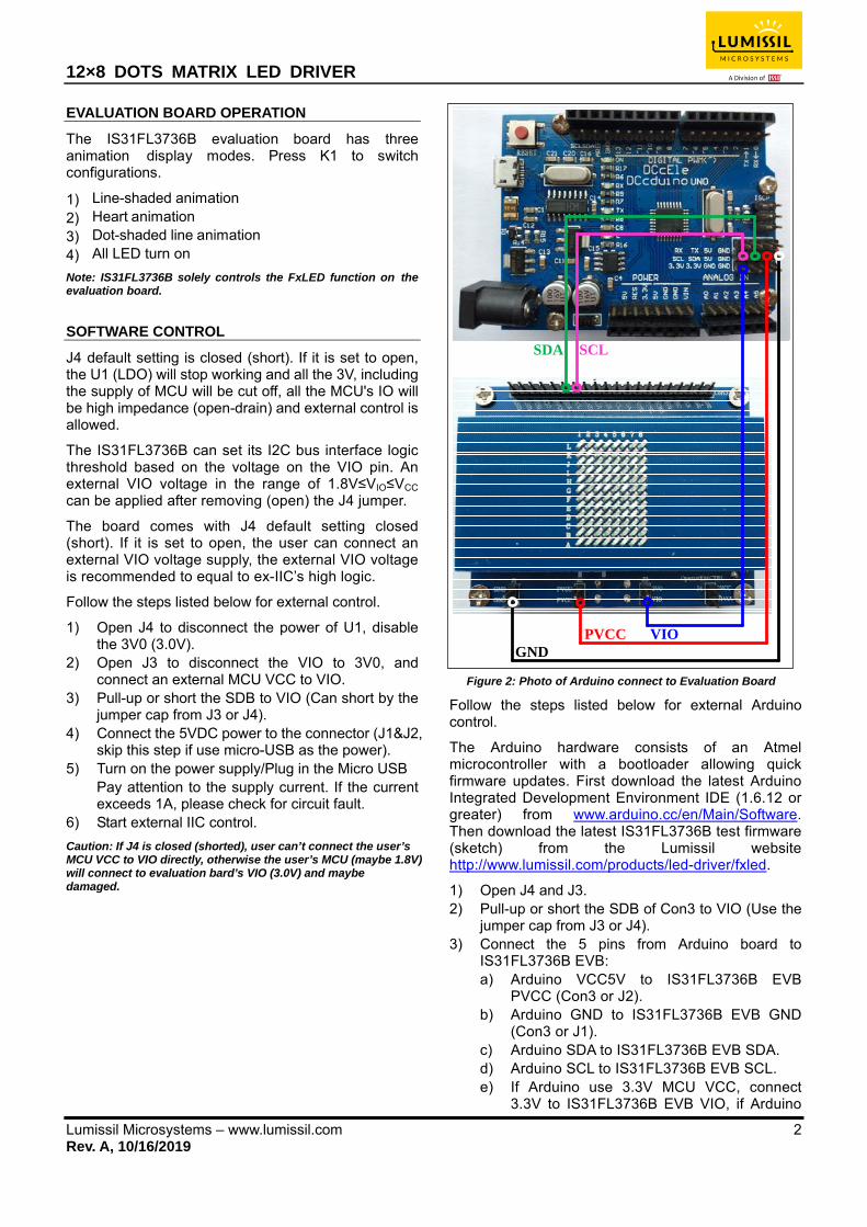
SDA SCL
PVCC VIOGND
Figure 2: Photo of Arduino connect to Evaluation Board
Follow the steps listed below for external Arduino control.
The Arduino hardware consists of an Atmel microcontroller with a bootloader allowing quick firmware updates. First download the latest Arduino Integrated Development Environment IDE (1.6.12 or greater) from www.arduino.cc/en/Main/Software. Then download the latest IS31FL3736B test firmware (sketch) from the Lumissil website http://www.lumissil.com/products/led-driver/fxled.
1) Open J4 and J3. 2) Pull-up or short the SDB of Con3 to VIO (Use the
jumper cap from J3 or J4). 3) Connect the 5 pins from Arduino board to
IS31FL3736B EVB: a) Arduino VCC5V to IS31FL3736B EVB
PVCC (Con3 or J2). b) Arduino GND to IS31FL3736B EVB GND
(Con3 or J1). c) Arduino SDA to IS31FL3736B EVB SDA. d) Arduino SCL to IS31FL3736B EVB SCL. e) If Arduino use 3.3V MCU VCC, connect
3.3V to IS31FL3736B EVB VIO, if Arduino

12×8 DOTS MATRIX LED DRIVER
Lumissil Microsystems – www.lumissil.com 3 Rev. A, 10/16/2019
use 5.0V MCU VCC, connect 5.0V to EVB VIO. (Arduino UNO MCU VCC is 5V, so SDB can be 5V or 3.3V)
4) Use the test code in appendix I or Download the test firmware (sketch) form Lumissil website, a .txt file and copy the code to Arduino IDE and download to Arduino.
5) Run the Arduino code and initial mode is change the brightness every second.
6) Default 31FL3736B device address is 0xA0 (ADDR1=LOW, ADDR2=GND), if user want to change the device address, use the AD1 in Con3 a) AD1=VIO or PVCC, device address=0xA6. b) AD1=SCL, device address=0xA2. c) AD1=SDA, device address=0xA4. ADDR2 pin is fixed to GND so user can’t change it.
Please refer to the datasheet to get more information about IS31FL3736B.
12×8 DOTS MATRIX LED DRIVER
Lumissil Microsystems – www.lumissil.com 4 Rev. A, 10/16/2019
LED Array
CS
1
CS
2
CS
3
CS
4
CS
5
CS
6
CS
7
CS
8
SW1
SW2
SW3
SW4
SW5
SW6
SW7
SW8
SW9
SW10
SW11
SW12
LED1 LED2 LED3 LED4 LED5 LED6 LED7 LED8
LED9 LED10 LED11 LED12 LED13 LED14 LED15 LED16
LED17 LED18 LED19 LED20 LED21 LED22 LED23 LED24
LED25 LED26 LED27 LED28 LED29 LED30 LED31 LED32
LED33 LED34 LED35 LED36 LED37 LED38 LED39 LED40
LED41 LED42 LED43 LED44 LED45 LED46 LED47 LED48
LED65 LED66 LED67 LED68 LED69 LED70 LED71 LED72
LED73 LED74 LED75 LED76 LED77 LED78 LED79 LED80
LED81 LED82 LED83 LED84 LED85 LED86 LED87 LED88
LED89 LED90 LED91 LED92 LED93 LED94 LED95 LED96
LED49 LED50 LED51 LED52 LED53 LED54 LED55 LED56
LED57 LED58 LED59 LED60 LED61 LED62 LED63 LED64
VBAT1
PC13-ANTI_TAMP2
PC14-OSC32_IN3
PC15-OSC32_OUT4
OSC_IN5
OSC_OUT6
NRST7
VSSA8
VDDA9
PA0-WKUP/ADC_IN0/TIM2_CH1_ETR10
PA1/ADC_IN1/TIM2_CH211
PA2/USART2_TX/ADC_IN2/TIM2_CH312
PA3/USART2_RX/ADC_IN3/TIM2_CH413
PA4/SPI1_NSS/ADC_IN414
PA5/SPI1_SCK/ADC_IN515
PA6/SPI1_MISO/ADC_IN6/TIM3_CH116
PA7/SPI1_MOSI/ADC_IN7/TIM3_CH217
PB0/ADC_IN8/TIM3_CH318
PB1/ADC_IN9/TIM3_CH419
PB2/BOOT120
PB10/I2C2_SCL/USART3_TX21
PB11/I2C2_SDA/USART3_RX22
VSS_123
VDD_124
PB12/SPI2_NSS/TIM1_BKIN25
PB13/SPI2_SCK/TIM1_CH1N26PB14/SPI2_MISO/TIM1_CH2N27
PB15/SPI2_MOSI/TIM1_CH3N28
PA8/TIM1_CH1/MCO29
PA9/USART1_TX/TIM1_CH2 30PA10/USART1_RX/TIM1_CH3
31PA11/CANRX/USBDM/TIM1_CH4
32PA12/CANTX/USBDP/TIM1_ETR 33
PA13/JTMS/SWDIO34
VSS_235
VDD_2 36PA14/JTCK/SWCLK
37PA15/JTDI
38PB3/JTDO
39PB4/JNTRST40
PB541
PB6/I2C1_SCL/TIM4_CH142PB7/I2C1_SDA/TIM4_CH243
BOOT044
PB8/TIM4_CH345
PB9/TIM4_CH4 46VSS_3
47VDD_3
48U2
STM32F103C8T6
OSC_INOSC_OUT
GND
3V
SDASCL
INTB
USB_DMUSB_DPDIOGND3V
GND
Y18M
33P
C7
33P
C6
OSC_IN
OSC_OUT
10nF
C2
VDD1
GND2
SD3
BP4
VOUT5
U1
LDO
1uFC1
3V
CLK
GND
1uFC3
3V0.1uF
C9
0.1uF
C8
MCU
3V Power
100KR11
20KR5
OSC
100KR8
4.7KR6
4.7KR12
K1
GND
1uFC5
GND
0.1uF
C10
10KR1
100KR7
100KR10
1234567891011121314151617181920
CON3
12
J112
J2
12
J3
Header 2H12
J4
Header 2H
GNDPVCC
VIO
U1 VCC
U1 VCC
GNDGNDCLKDIO3.3VIICRST
INTBSDASCLAD1AD1GNDSCLSDAPVCCVIOSDBGNDGND
PVCC3V
NCR9
3V
0.1uF
C11
SDB
91KR13
10KR14
3V
Micro USB
VCC1
USB_DM2
USB_DP3
NC4
GND5
Con4
10uF
C4
PVCC
GND
22R
R4
22R
R2
USB_DM
USB_DP
1.5K
R33V
USB_DMUSB_DP
10uF
C12
D1
DFL240
GND
11
22 33
44
55 66
77
8899
1010
11111212
Con2
11
22
3 3
44
55
6 6
77
88
99
1010
1111
1212
1313
1414
1515
1616
Con1
CS1CS2CS3CS4CS5CS6CS7CS8CS9CS10CS11CS12CS13CS14CS15CS16
SW1 SW2SW3 SW4SW5 SW6SW7 SW8SW9 SW10SW11 SW12
IO
PVCC
GND
GND
GND
VIO
GND
GND
GND
SW1SW2SW3SW4SW5SW6SW7SW8SW9SW10SW11SW12
CS1CS2CS3CS4CS5CS6CS7CS8
VIO
SDASCLINTBSDB
RSET
AD
IICRST
3V
SW11
SW22
SW33
PGND4
SW45
SW56
SW67SW78
SW89
SW910
PGND11
SW1012
SW1113
SW1214
CS115
CS216CS318
CS419
PVCC17
CS521CS622
CS724
CS825
PVCC23
AGND26
RSET30
AVCC28
DVCC27
VIO31
SDA33
SCL34
ADDR135
ADDR236
INTB37
SDB38
IICRS39
GND40
SYNC32
U3
IS31FL3736B
SYNC
SYNC
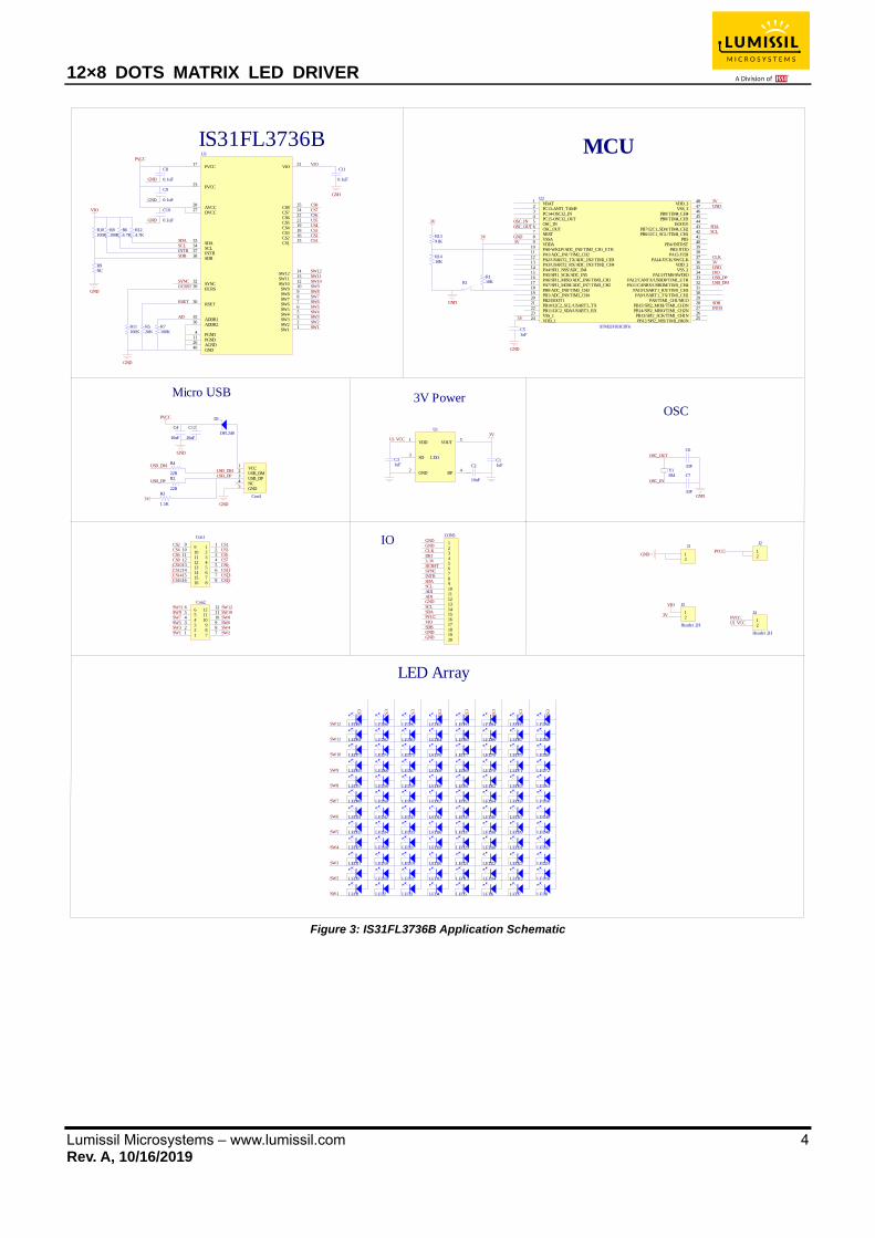
Figure 3: IS31FL3736B Application Schematic

12×8 DOTS MATRIX LED DRIVER
Lumissil Microsystems – www.lumissil.com 5 Rev. A, 10/16/2019
BILL OF MATERIALS
Name Symbol Description Qty Supplier Part No.
LDO U1 Reduced voltage 1 SGMICRO SGM2019-3.3V
MCU U2 Microcontroller 1 STM STM32F103C8T6
LED Driver U3 Matrix LED Driver 1 Lumissil IS31FL3736B
LED LED1~LED96 Blue LED, SMD 96 Everlight 9-217/BHC-ZL1M2RY/3T
Diode D1 Diode, SMD 1 DIODES DFLS240
Crystal Y1 Crystal, 8MHz 1 JB HC-49S
Resistor R1,R14 RES,10k,1/16W,±5%,SMD 2 Yageo RC0603JR-0710KL
Resistor R2,R4 RES,22R,1/16W,±5%,SMD 2 Yageo RC0603JR-0722RL
Resistor R3 RES,1.5k,1/16W,±5%,SMD 1 Yageo RC0603JR-071K5L
Resistor R5 RES,20k,1/16W,±5%,SMD 1 Yageo RC0603JR-0720KL
Resistor R6,R12 RES,1k,1/16W,±5%,SMD 2 Yageo RC0603JR-0701KL
Resistor R7,R8,R10,R11 RES,100k,1/16W,±5%,SMD 4 Yageo RC0603JR-07100KL
Resistor R9 NC 0
Resistor R13 RES,91k,1/16W,±5%,SMD 1 Yageo RC0603JR-07910KL
Capacitor C1,C3,C5 CAP,1µF,16V,±20%,SMD 3 Yageo CC0603KKX7R9BB105
Capacitor C2 CAP,10pF,16V,±20%,SMD 1 Yageo CC0603KKX7R9BB100
Capacitor C4,C12 CAP,10µF,16V, ±20%,SMD 2 Yageo CC0603KKX7R9BB106
Capacitor C6,C7 CAP,33pF,16V,±20%,SMD 2 Yageo CC0603KKX7R9BB330
Capacitor C8,C9,C10,C11 CAP,0.1µF,16V,±20%,SMD 3 Yageo CC0603KKX7R9BB104
Button K1 Button 1
Bill of Materials, refer to Figure 3 above.
12×8 DOTS MATRIX LED DRIVER
Lumissil Microsystems – www.lumissil.com 6 Rev. A, 10/16/2019
0
0 0
0
22 181716151413121110987654321
2
111
0
0 0
0 2
12
1 2
1
0
1
3
2
816
715
14
13
12
11
10
9
6
5
4
3
2
1
12
11
10
9
8
7
6
5
4
3
2
1
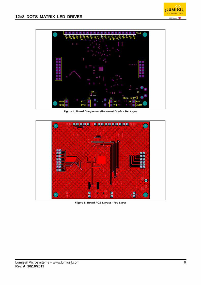
Figure 4: Board Component Placement Guide - Top Layer
0
0 0
0
21
22 181716151413121110987654321
2
111
0
0 0
0 2
12
1 2
1
0
1
3
2
816
715
14
13
12
11
10
9
6
5
4
3
2
1
12
11
10
9
8
7
6
5
4
3
2
1
Figure 5: Board PCB Layout - Top Layer
12×8 DOTS MATRIX LED DRIVER
Lumissil Microsystems – www.lumissil.com 7 Rev. A, 10/16/2019
0
0 0
0
22 181716151413121110987654321
2
111
0
0 0
0 2
12
1 2
1
0
1
3
2
816
715
14
13
12
11
10
9
6
5
4
3
2
1
12
11
10
9
8
7
6
5
4
3
2
1
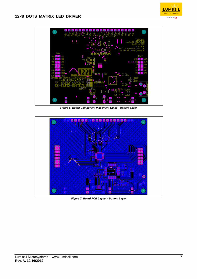
Figure 6: Board Component Placement Guide - Bottom Layer
0
0 0
0
2 1
21
21
41
2
1
2
1
22 181716151413121110987654321
2
1
2
1 2
1
2
111
0
0 0
0 2
12
1 2
1
2
1
2
1
2
1
2
1
2
1
21
3
4
2
1
2 1
21
21
2
1
2
1
2
1
2
1
2
1 0
1
3
2
1 1 1 1 1
1
2
1
816
715
14
13
12
11
10
9
6
5
4
3
2
1
12
11
10
9
8
7
6
5
4
3
2
1
1 2
12
21
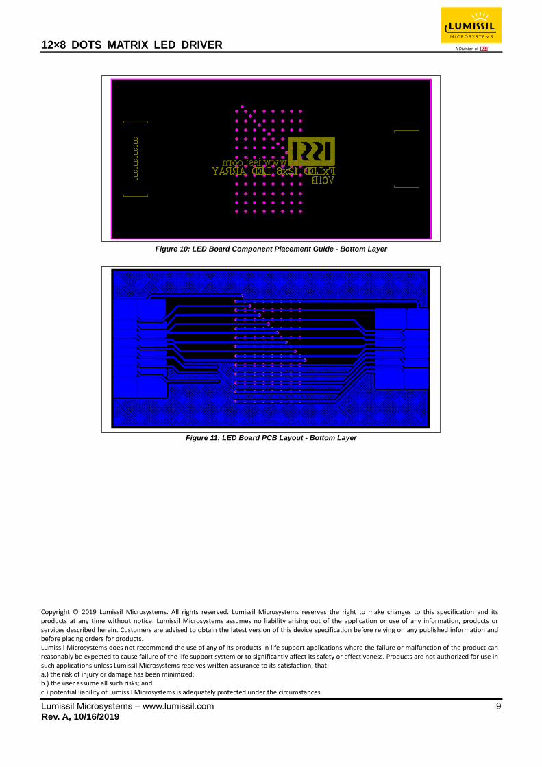
Figure 7: Board PCB Layout - Bottom Layer

12×8 DOTS MATRIX LED DRIVER
Lumissil Microsystems – www.lumissil.com 8 Rev. A, 10/16/2019
Figure 8: LED Board Component Placement Guide - Top Layer
2
1
2
1
2
1
2
1
2
1
2
1
2
1
2
1
2
1
2
1
2
1
2
1
2
1
2
1
2
1
2
1
2
1
2
1
2
1
2
1
2
1
2
1
2
1
2
1
2
1
2
1
2
1
2
1
2
1
2
1
2
1
2
1
2
1
2
1
2
1
2
1
2
1
2
1
2
1
2
1
2
1
2
1
2
1
2
1
2
1
2
1
2
1
2
1
2
1
2
1
2
1
2
1
2
1
2
1
2
1
2
1
2
1
2
1
2
1
2
1
2
1
2
1
2
1
2
1
2
1
2
1
2
1
2
1
2
1
2
1
2
1
2
1
2
1
2
1
2
1
2
1
2
1
2
1
2
1
2
1
2
1
2
1
2
1
2
1
2
1
2
1
2
1
2
1
2
1
2
1
2
1
2
1
2
1
2
1
2
1
2
1
Figure 9: LED Board PCB Layout - Top Layer
12×8 DOTS MATRIX LED DRIVER
Lumissil Microsystems – www.lumissil.com 9 Rev. A, 10/16/2019
Figure 10: LED Board Component Placement Guide - Bottom Layer
16
15
14
13
12
11
10
1
2
3
4
5
6
7
8
9
1
2
3
4
5
6 12
11
10
9
8
7
Figure 11: LED Board PCB Layout - Bottom Layer
Copyright © 2019 Lumissil Microsystems. All rights reserved. Lumissil Microsystems reserves the right to make changes to this specification and its products at any time without notice. Lumissil Microsystems assumes no liability arising out of the application or use of any information, products or services described herein. Customers are advised to obtain the latest version of this device specification before relying on any published information and before placing orders for products. Lumissil Microsystems does not recommend the use of any of its products in life support applications where the failure or malfunction of the product can reasonably be expected to cause failure of the life support system or to significantly affect its safety or effectiveness. Products are not authorized for use in such applications unless Lumissil Microsystems receives written assurance to its satisfaction, that: a.) the risk of injury or damage has been minimized; b.) the user assume all such risks; and c.) potential liability of Lumissil Microsystems is adequately protected under the circumstances
12×8 DOTS MATRIX LED DRIVER
Lumissil Microsystems – www.lumissil.com 10 Rev. A, 10/16/2019
REVISION HISTORY
Revision Detail Information Date
A Initial release 2019.10.16
12×8 DOTS MATRIX LED DRIVER
Lumissil Microsystems – www.lumissil.com 11 Rev. A, 10/16/2019
APPENDIX Ⅰ: IS31FL3736B Arduino Test Code V01A
#include<Wire.h>
#include<avr/pgmspace.h>
#define Addr_GND_GND 0xa0//AD1 open (R7 pull-low), ADDR2=GND
#define Addr_GND_VCC 0xa6//AD1 = VIO, ADDR2=GND
#define Addr_GND_SCL 0xa2//AD1 = SCL, ADDR2=GND
#define Addr_GND_SDA 0xa4//AD1 = SDA, ADDR2=GND
void setup()
{
Wire.begin();
Wire.setClock(800000);//I2C 800kHz
IS31FL3736B_init();
}
void loop()
{
IS31FL3736B_Test_mode1();//breath mode
}
void IS_IIC_WriteByte(uint8_t Dev_Add,uint8_t Reg_Add,uint8_t Reg_Dat)
{
Wire.beginTransmission(Dev_Add/2); // transmit to device address
Wire.write(Reg_Add); // sends register address
Wire.write(Reg_Dat); // sends register data
Wire.endTransmission(); // stop transmitting
}
void IS31FL3736B_init(void)//white LED
{
uint8_t i;
IS_IIC_WriteByte(Addr_GND_GND,0xFE,0xc5);//Unlock FDh
IS_IIC_WriteByte(Addr_GND_GND,0xFD,0x03);//Turn to page 3: function registers
IS_IIC_WriteByte(Addr_GND_GND,0x00,0x00);//Enable software shutdown
IS_IIC_WriteByte(Addr_GND_GND,0xFE,0xc5);//Unlock FDh
IS_IIC_WriteByte(Addr_GND_GND,0xFD,0x00);// Turn to page 0: control registers
for(i=0;i<0x18;i=i+1)IS_IIC_WriteByte(Addr_GND_GND,i,0xff);//open all LED
//can use buffer write type as figure 7 in datasheet
IS_IIC_WriteByte(Addr_GND_GND,0xFE,0xc5);//unlock FDh
IS_IIC_WriteByte(Addr_GND_GND,0xFD,0x01);//Turn to page 1: PWM registers
for(i=0;i<192;i++)IS_IIC_WriteByte(Addr_GND_GND,i,0x00);//Set PWM data to 0
//can use buffer write type as figure 7 in datasheet
12×8 DOTS MATRIX LED DRIVER
Lumissil Microsystems – www.lumissil.com 12 Rev. A, 10/16/2019
IS_IIC_WriteByte(Addr_GND_GND,0xFE,0xc5);//unlock FDh
IS_IIC_WriteByte(Addr_GND_GND,0xFD,0x03);//Turn to page 3: function registers
IS_IIC_WriteByte(Addr_GND_GND,0x00,0x01);//Release software shutdown to normal operation
IS_IIC_WriteByte(Addr_GND_GND,0x01,0xff);//global current
}
void IS31FL3736B_Test_mode1(void)//white LED
{
uint8_t i;
while(1)
{
IS_IIC_WriteByte(Addr_GND_GND,0xFE,0xc5);//unlock FDh
IS_IIC_WriteByte(Addr_GND_GND,0xFD,0x01);//Turn to page 1: PWM registers
for(i=0;i<192;i++)IS_IIC_WriteByte(Addr_GND_GND,i,0x10);//update all PWM with 0x10
delay(1000); // wait for a second
IS_IIC_WriteByte(Addr_GND_GND,0xFE,0xc5);//unlock FDh
IS_IIC_WriteByte(Addr_GND_GND,0xFD,0x01);//Turn to page 1: PWM registers
for(i=0;i<192;i++)IS_IIC_WriteByte(Addr_GND_GND,i,0x80); //update all PWM with 0x80
delay(1000); // wait for a second
}
}