125V/2A, High-Speed, Half-Bridge MOSFET Drivers 125V/2A, High-Speed, Half-Bridge MOSFET Drivers 2...
20
General Description The MAX5062/MAX5063/MAX5064 high-frequency, 125V half-bridge, n-channel MOSFET drivers drive high- and low-side MOSFETs in high-voltage applications. These drivers are independently controlled and their 35ns typical propagation delay, from input to output, are matched to within 3ns (typ). The high-voltage operation with very low and matched propagation delay between drivers, and high source/sink current capabilities in a thermally enhanced package make these devices suit- able for the high-power, high-frequency telecom power converters. The 125V maximum input voltage range pro- vides plenty of margin over the 100V input transient requirement of telecom standards. A reliable on-chip bootstrap diode connected between V DD and BST elimi- nates the need for an external discrete diode. The MAX5062A/C and the MAX5063A/C offer both nonin- verting drivers (see the Selector Guide ). The MAX5062B/D and the MAX5063B/D offer a noninverting high-side driver and an inverting low-side driver. The MAX5064A/B offer two inputs per driver that can be either inverting or noninverting. The MAX5062A/B/C/D and the MAX5064A feature CMOS (V DD / 2) logic inputs. The MAX5063A/B/C/D and the MAX5064B feature TTL logic inputs. The MAX5064A/B include a break-before- make adjustment input that sets the dead time between drivers from 16ns to 95ns. The drivers are available in the industry-standard 8-pin SO footprint and pin configura- tion, and a thermally enhanced 8-pin SO and 12-pin (4mm x 4mm) thin QFN packages. All devices operate over the -40°C to +125°C automotive temperature range. Applications Telecom Half-Bridge Power Supplies Two-Switch Forward Converters Full-Bridge Converters Active-Clamp Forward Converters Power-Supply Modules Motor Control Features ♦ HIP2100/HIP2101 Pin Compatible (MAX5062A/ MAX5063A) ♦ Up to 125V Input Operation ♦ 8V to 12.6V V DD Input Voltage Range ♦ 2A Peak Source and Sink Current Drive Capability ♦ 35ns Typical Propagation Delay ♦ Guaranteed 8ns Propagation Delay Matching Between Drivers ♦ Programmable Break-Before-Make Timing (MAX5064) ♦ Up to 1MHz Combined Switching Frequency while Driving 100nC Gate Charge (MAX5064) ♦ Available in CMOS (V DD / 2) or TTL Logic-Level Inputs with Hysteresis ♦ Up to 15V Logic Inputs Independent of Input Voltage ♦ Low 2.5pF Input Capacitance ♦ Instant Turn-Off of Drivers During Fault or PWM Start-Stop Synchronization (MAX5064) ♦ Low 200μA Supply Current ♦ Versions Available With Combination of Noninverting and Inverting Drivers (MAX5062B/D and MAX5063B/D) ♦ Available in 8-Pin SO, Thermally Enhanced SO, and 12-Pin Thin QFN Packages MAX5062/MAX5063/MAX5064 125V/2A, High-Speed, Half-Bridge MOSFET Drivers ________________________________________________________________ Maxim Integrated Products 1 PART TEMP RANGE PIN- PACKAGE TOP MARK PKG CODE MAX5062AASA -40°C to +125°C 8 SO — S8-5 MAX5062BASA -40°C to +125°C 8 SO — S8-5 MAX5062CASA -40°C to +125°C 8 SO-EP* — S8E-14 MAX5062DASA -40°C to +125°C 8 SO-EP* — S8E-14 Ordering Information PART HIGH-SIDE DRIVER LOW-SIDE DRIVER LOGIC LEVELS PIN COMPATIBLE MAX5062AASA Noninverting Noninverting CMOS (V DD / 2) HIP 2100IB MAX5062BASA Noninverting Inverting CMOS (V DD / 2) — MAX5062CASA Noninverting Noninverting CMOS (V DD / 2) — MAX5062DASA Noninverting Inverting CMOS (V DD / 2) — Selector Guide 19-3502; Rev 5; 5/07 For pricing, delivery, and ordering information, please contact Maxim/Dallas Direct! at 1-888-629-4642, or visit Maxim’s website at www.maxim-ic.com. Selector Guide continued at end of data sheet. *EP = Exposed paddle. Devices are available in both leaded and lead-free packaging. Specify lead-free by replacing “-T” with “+T” when ordering. Ordering Information continued at end of data sheet.
Transcript of 125V/2A, High-Speed, Half-Bridge MOSFET Drivers 125V/2A, High-Speed, Half-Bridge MOSFET Drivers 2...

General DescriptionThe MAX5062/MAX5063/MAX5064 high-frequency,125V half-bridge, n-channel MOSFET drivers drive high-and low-side MOSFETs in high-voltage applications.These drivers are independently controlled and their35ns typical propagation delay, from input to output, arematched to within 3ns (typ). The high-voltage operationwith very low and matched propagation delay betweendrivers, and high source/sink current capabilities in athermally enhanced package make these devices suit-able for the high-power, high-frequency telecom powerconverters. The 125V maximum input voltage range pro-vides plenty of margin over the 100V input transientrequirement of telecom standards. A reliable on-chipbootstrap diode connected between VDD and BST elimi-nates the need for an external discrete diode.
The MAX5062A/C and the MAX5063A/C offer both nonin-verting drivers (see the Selector Guide). TheMAX5062B/D and the MAX5063B/D offer a noninvertinghigh-side driver and an inverting low-side driver. TheMAX5064A/B offer two inputs per driver that can beeither inverting or noninverting. The MAX5062A/B/C/Dand the MAX5064A feature CMOS (VDD / 2) logic inputs.The MAX5063A/B/C/D and the MAX5064B feature TTLlogic inputs. The MAX5064A/B include a break-before-make adjustment input that sets the dead time betweendrivers from 16ns to 95ns. The drivers are available in theindustry-standard 8-pin SO footprint and pin configura-tion, and a thermally enhanced 8-pin SO and 12-pin(4mm x 4mm) thin QFN packages. All devices operateover the -40°C to +125°C automotive temperature range.
ApplicationsTelecom Half-Bridge Power Supplies
Two-Switch Forward Converters
Full-Bridge Converters
Active-Clamp Forward Converters
Power-Supply Modules
Motor Control
Features♦ HIP2100/HIP2101 Pin Compatible (MAX5062A/
MAX5063A)♦ Up to 125V Input Operation♦ 8V to 12.6V VDD Input Voltage Range♦ 2A Peak Source and Sink Current Drive Capability♦ 35ns Typical Propagation Delay♦ Guaranteed 8ns Propagation Delay Matching
Between Drivers♦ Programmable Break-Before-Make Timing
(MAX5064)♦ Up to 1MHz Combined Switching Frequency while
Driving 100nC Gate Charge (MAX5064)♦ Available in CMOS (VDD / 2) or TTL Logic-Level
Inputs with Hysteresis♦ Up to 15V Logic Inputs Independent of Input
Voltage♦ Low 2.5pF Input Capacitance♦ Instant Turn-Off of Drivers During Fault or PWM
Start-Stop Synchronization (MAX5064)♦ Low 200µA Supply Current♦ Versions Available With Combination of
Noninverting and Inverting Drivers (MAX5062B/Dand MAX5063B/D)
♦ Available in 8-Pin SO, Thermally Enhanced SO,and 12-Pin Thin QFN Packages
MA
X5
06
2/M
AX
50
63
/MA
X5
06
4
125V/2A, High-Speed, Half-Bridge MOSFET Drivers
________________________________________________________________ Maxim Integrated Products 1
PART TEMP RANGEPIN-PACKAGE
TOPMARK
PKGCODE
MAX5062AASA -40°C to +125°C 8 SO — S8-5
MAX5062BASA -40°C to +125°C 8 SO — S8-5
MAX5062CASA -40°C to +125°C 8 SO-EP* — S8E-14
MAX5062DASA -40°C to +125°C 8 SO-EP* — S8E-14
Ordering Information
PART HIGH-SIDE DRIVER LOW-SIDE DRIVER LOGIC LEVELS PIN COMPATIBLE
MAX5062AASA Noninverting Noninverting CMOS (VDD / 2) HIP 2100IBMAX5062BASA Noninverting Inverting CMOS (VDD / 2) —
MAX5062CASA Noninverting Noninverting CMOS (VDD / 2) —
MAX5062DASA Noninverting Inverting CMOS (VDD / 2) —
Selector Guide
19-3502; Rev 5; 5/07
For pricing, delivery, and ordering information, please contact Maxim/Dallas Direct! at 1-888-629-4642, or visit Maxim’s website at www.maxim-ic.com.
Selector Guide continued at end of data sheet.
*EP = Exposed paddle.Devices are available in both leaded and lead-free packaging.Specify lead-free by replacing “-T” with “+T” when ordering.Ordering Information continued at end of data sheet.

MA
X5
06
2/M
AX
50
63
/MA
X5
06
4
125V/2A, High-Speed, Half-Bridge MOSFET Drivers
2 _______________________________________________________________________________________
ABSOLUTE MAXIMUM RATINGS
ELECTRICAL CHARACTERISTICS(VDD = VBST = +8V to +12.6V, VHS = GND = 0V, BBM = open, TA = -40°C to +125°C, unless otherwise noted. Typical values are atVDD = VBST = +12V and TA = +25°C.) (Note 1)
Stresses beyond those listed under “Absolute Maximum Ratings” may cause permanent damage to the device. These are stress ratings only, and functionaloperation of the device at these or any other conditions beyond those indicated in the operational sections of the specifications is not implied. Exposure toabsolute maximum rating conditions for extended periods may affect device reliability.
(All voltages referenced to GND, unless otherwise noted.)VDD, IN_H, IN_L, IN_L+, IN_L-, IN_H+, IN_H-........-0.3V to +15VDL, BBM .....................................................-0.3V to (VDD + 0.3V)HS............................................................................-5V to +130VDH to HS.....................................................-0.3V to (VDD + 0.3V)BST to HS ...............................................................-0.3V to +15VAGND to PGND (MAX5064) ..................................-0.3V to +0.3VdV/dt at HS ........................................................................50V/nsContinuous Power Dissipation (TA = +70°C)
8-Pin SO (derate 5.9mW/°C above +70°C)...............470.6mW
8-Pin SO with Exposed Pad (derate 19.2mW/°Cabove +70°C)* ....................................................1538.5mW
12-Pin Thin QFN (derate 24.4mW/°C above +70°C)* ....................................................1951.2mW
Maximum Junction Temperature .....................................+150°COperating Temperature Range .........................-40°C to +125°CStorage Temperature Range .............................-65°C to +150°CLead Temperature (soldering, 10s) .................................+300°C
*Per JEDEC 51 standard multilayer board.
PARAMETER SYMBOL CONDITIONS MIN TYP MAX UNITS
POWER SUPPLIES
Operating Supply Voltage VDD (Note 2) 8.0 12.6 V
MAX5062_/MAX5063_
70 140VDD Quiescent Supply Current IDD
IN_H = IN_L = GND(no switching)
MAX5064_ 120 260
µA
VDD Operating Supply Current IDDO fSW = 500kHz, VDD = +12V 3 mA
BST Quiescent Supply Current IBST IN_H = IN_L = GND (no switching) 15 40 µA
BST Operating Supply Current IBSTO fSW = 500kHz, VDD = VBST = +12V 3 mA
UVLO (VDD to GND) UVLOVDD VDD rising 6.5 7.3 8.0 V
UVLO (BST to HS) UVLOBST BST rising 6.0 6.9 7.8 V
UVLO Hysteresis 0.5 V
LOGIC INPUT
MAX5062_/MAX5064A,CMOS (VDD / 2) version
0.67 xVDD
0.55 xVDDInput-Logic High VIH_
MAX5063_/MAX5064B, TTL version 2 1.65
V
MAX5062_/MAX5064A,CMOS (VDD / 2) version
0.4 xVDD
0.33 xVDDInput-Logic Low VIL_
MAX5063_/MAX5064B, TTL version 1.4 0.8
V
MAX5062_/MAX5064A,CMOS (VDD / 2) version
1.6Logic-Input Hysteresis VHYS
MAX5063_/MAX5064B, TTL version 0.25
V

MA
X5
06
2/M
AX
50
63
/MA
X5
06
4
125V/2A, High-Speed, Half-Bridge MOSFET Drivers
_______________________________________________________________________________________ 3
ELECTRICAL CHARACTERISTICS (continued)(VDD = VBST = +8V to +12.6V, VHS = GND = 0V, BBM = open, TA = -40°C to +125°C, unless otherwise noted. Typical values are atVDD = VBST = +12V and TA = +25°C.) (Note 1)
PARAMETER SYMBOL CONDITIONS MIN TYP MAX UNITS
VIN_H+, VIN_L+ = 0V
VIN_L = VDD for MAX5062B/D, MAX5063B/D
VIN_H-, VIN_L-, VIN_H = VDDLogic-Input Current I_IN
VIN_L = 0V for MAX5062A/C, MAX5063A/C
-1 0.001 +1 µA
IN_H+, IN_L+ IN_H, to GND
IN_L to VDD for MAX5062B/D,MAX5063B/D
IN_H-, IN_L-, IN_H, to VDD
Input Resistance RIN
IN_L for MAX5062A/C, MAX5063A/C to GND
1 MΩ
Input Capacitance CIN 2.5 pF
HIGH-SIDE GATE DRIVER
HS Maximum Voltage VHS_MAX 125 V
BST Maximum Voltage VBST_MAX 140 V
TA = +25°C 2.5 3.3Driver Output Resistance(Sourcing)
RON_HPVDD = 12V, IDH = 100mA(sourcing) TA = +125°C 3.5 4.6
Ω
TA = +25°C 2.1 2.8Driver Output Resistance(Sinking)
RON_HNVDD = 12V, IDH = 100mA(sinking) TA = +125°C 3.2 4.2
Ω
DH Reverse Current (LatchupProtection)
(Note 3) 400 mA
Power-Off Pulldown ClampVoltage
VBST = 0V or floating, IDH = 1mA (sinking) 0.94 1.16 V
Peak Output Current (Sourcing) CL = 10nF, VDH = 0V 2 A
Peak Output Current (Sinking)IDH_PEAK
CL = 10nF, VDH = 12V 2 A
LOW-SIDE GATE DRIVER
TA = +25°C 2.5 3.3Driver Output Resistance(Sourcing)
RON_LPVDD = 12V, IDL = 100mA(sourcing) TA = +125°C 3.5 4.6
Ω
TA = +25°C 2.1 2.8Driver Output Resistance(Sinking)
RON_LNVDD = 12V, IDL = 100mA(sinking) TA = +125°C 3.2 4.2
Ω
Reverse Current at DL (LatchupProtection)
(Note 3) 400 mA
Power-Off Pulldown ClampVoltage
VDD = 0V or floating, IDL = 1mA (sinking) 0.95 1.16 V
Peak Output Current (Sourcing) IPK_LP CL = 10nF, VDL = 0V 2 A
Peak Output Current (Sinking) IPK_LN CL = 10nF, VDL = 12V 2 A
INTERNAL BOOTSTRAP DIODE
Forward Voltage Drop Vf IBST = 100mA 0.91 1.11 V
Turn-On and Turn-Off Time tR IBST = 100mA 40 ns

MA
X5
06
2/M
AX
50
63
/MA
X5
06
4
125V/2A, High-Speed, Half-Bridge MOSFET Drivers
4 _______________________________________________________________________________________
Note 1: All devices are 100% tested at TA = +125°C. Limits over temperature are guaranteed by design.Note 2: Ensure that the VDD-to-GND or BST-to-HS voltage does not exceed 13.2V.Note 3: Guaranteed by design, not production tested.Note 4: Break-before-make time is calculated by tBBM = 8ns x (1 + RBBM / 10kΩ).Note 5: See the Minimum Pulse Width section.
ELECTRICAL CHARACTERISTICS (continued)(VDD = VBST = +8V to +12.6V, VHS = GND = 0V, BBM = open, TA = -40°C to +125°C, unless otherwise noted. Typical values are atVDD = VBST = +12V and TA = +25°C.) (Note 1)
PARAMETER SYMBOL CONDITIONS MIN TYP MAX UNITS
SWITCHING CHARACTERISTICS FOR HIGH- AND LOW-SIDE DRIVERS (VDD = VBST = +12V)
CL = 1000pF 7
CL = 5000pF 33Rise Time tRCL = 10,000pF 65
ns
CL = 1000pF 7
CL = 5000pF 33Fall Time tFCL = 10,000pF 65
ns
CMOS 30 55Turn-On Propagation Delay Time tD_ON
Figure 1, CL = 1000pF(Note 3) TTL 35 63
ns
CMOS 30 55Turn-Off Propagation Delay Time tD_OFF
Figure 1, CL = 1000pF(Note 3) TTL 35 63
ns
Delay Matching BetweenInverting Input to Output andNoninverting Input to Output
tMATCH1CL = 1000pF, BBM open for MAX5064,Figure 1 (Note 3)
2 8 ns
Delay Matching Between Driver-Low and Driver-High
tMATCH2CL = 1000pF, BBM open for MAX5064,Figure 1 (Note 3)
2 8 ns
RBBM = 10kΩ 16
RBBM = 47kΩ (Notes 3, 4) 40 56 72Break-Before-Make Accuracy(MAX5064 Only)
RBBM = 100kΩ 95
ns
Internal Nonoverlap 1 ns
VDD = VBST = 12V 135Minimum Pulse-Width Input Logic(High or Low) (Note 5)
tPW-MINVDD = VBST = 8V 170
ns

MA
X5
06
2/M
AX
50
63
/MA
X5
06
4
125V/2A, High-Speed, Half-Bridge MOSFET Drivers
_______________________________________________________________________________________ 5
UNDERVOLTAGE LOCKOUT(VDD AND VBST RISING) vs. TEMPERATURE
MAX
5062
/3/4
toc0
1
TEMPERATURE (°C)
UVLO
(V)
1109565 80-10 5 20 35 50-25
6.6
6.7
6.8
6.9
7.0
7.1
7.2
7.3
7.4
7.5
6.5-40 125
UVLOVDD
UVLOBST
VDD AND BST UNDERVOLTAGE LOCKOUTHYSTERESIS vs. TEMPERATURE
MAX
5062
/3/4
toc0
2
TEMPERATURE (°C)
UVLO
HYS
TERE
SIS
(V)
1109565 80-10 5 20 35 50-25
0.1
0.2
0.3
0.4
0.5
0.6
0.7
0.8
0.9
1.0
0-40 125
UVLOBSTHYSTERESIS
UVLOVDDHYSTERESIS
IDD vs. VDDMAX5062/3/4 toc03
40µs/div
VDD2V/div
500µA/div
0A
0V
IDD
MAX5064IN_L-, IN_H- = VDDIN_L+, IN_H+ = GND
IDDO + IBSTO vs. VDD(fSW = 250kHz)
MAX
5062
/3/4
toc0
4
VDD (V)
I DDO
+ I B
STO
(mA)
1210 113 4 5 6 7 8 91 2
1.00.80.60.40.2
1.21.41.61.82.02.22.42.62.83.0
00 13
0
60
40
20
80
100
120
140
160
180
200
0.5 0.70.6 0.8 0.9 1.0 1.1
INTERNAL BST DIODE(I-V) CHARACTERISTICS
MAX
5062
/3/4
toc0
5
VDD - VBST (V)
I DIO
DE (m
A)
TA = +125°C
TA = +25°C
TA = 0°C
TA = -40°C
0
60
40
20
80
100
120
140
160
0 42 6 8 101 53 7 9 11 12 13 14 15
VDD QUIESCENT CURRENTvs. VDD (NO SWITCHING)
MAX
5062
/3/4
toc0
6
VDD (V)
I DD
(µA)
TA = -40°C
TA = +125°CMAX5064
TA = +25°C, TA = 0°C
0
6
3
9
12
15
18
21
0 42 6 8 101 53 7 9 11 12 13 14 15
BST QUIESCENT CURRENTvs. BST VOLTAGE
MAX
5062
/3/4
toc0
7
VBST (V)
I BST
(µA)
VBST = VDD + 1V, NO SWITCHING
TA = +125°C
TA = -40°C, TA = 0°C, TA = +25°C
Typical Operating Characteristics(Typical values are at VDD = VBST = +12V and TA = +25°C, unless otherwise specified.)

MA
X5
06
2/M
AX
50
63
/MA
X5
06
4
125V/2A, High-Speed, Half-Bridge MOSFET Drivers
6 _______________________________________________________________________________________
VDD AND BST OPERATING SUPPLYCURRENT vs. FREQUENCY
MAX
5062
/3/4
toc0
8
FREQUENCY (kHz)
I DDO
+ I B
STO
(mA)
900700 800200 300 400 500 600100
1
2
3
4
5
6
7
8
9
10
00 1000
CL = 0
DH OR DL OUTPUT LOW VOLTAGE vs. TEMPERATURE
MAX
5062
/3/4
toc0
9
TEMPERATURE (°C)
OUTP
UT L
OW V
OLTA
GE (V
)
1109565 80-10 5 20 35 50-25
0.120.140.160.180.20
0.24
0.28
0.320.34
0.22
0.26
0.30
0.10-40 125
SINKING 100mA
DH OR DL FALL TIME vs. TEMPERATURE (CLOAD = 10nF)
MAX
5062
/3/4
toc1
2
TEMPERATURE (°C)
t F (n
s)
1109565 80-10 5 20 35 50-25
1020304050
70
11010090
120
60
80
0-40 125
VDD = VBST = 8V
VDD = VBST = 12V
DH OR DL RISE PROPAGATION DELAY vs. TEMPERATURE
MAX
5062
/3/4
toc1
3
TEMPERATURE (°C)
PROP
AGAT
ION
DELA
Y (n
s)
1109565 80-10 5 20 35 50-25
510152025
35
5560
30
4550
40
0-40 125
DH
DL
PEAK DH AND DLSOURCE/SINK CURRENT
MAX5062/3/4 toc10
1µs/div
DH OR DL5V/div
SINK AND SOURCECURRENT
2A/div
CL = 100nF
DH OR DL RISE TIME vs. TEMPERATURE (CL = 10nF)
MAX
5062
/3/4
toc1
1
TEMPERATURE (°C)
t R (n
s)
1109565 80-10 5 20 35 50-25
12
24
36
48
60
84
108
120
72
96
0-40 125
VDD = VBST = 8V
VDD = VBST = 12V
Typical Operating Characteristics (continued)(Typical values are at VDD = VBST = +12V and TA = +25°C, unless otherwise specified.)

MA
X5
06
2/M
AX
50
63
/MA
X5
06
4
125V/2A, High-Speed, Half-Bridge MOSFET Drivers
_______________________________________________________________________________________ 7
DH OR DL FALL PROPAGATION DELAY vs. TEMPERATURE
MAX
5062
/3/4
toc1
4
TEMPERATURE (°C)
PROP
AGAT
ION
DELA
Y (n
s)
1109565 80-10 5 20 35 50-25
510152025
35
5560
30
4550
40
0-40 125
DH
DL
BREAK-BEFORE-MAKEDEAD TIME vs. RBBM
MAX
5062
/3/4
toc1
5
RBBM (kΩ)
t BBM
(ns)
290210 25090 130 17050
25
50
75
100
125
175
250
150
200
225
010
MAX5064
BREAK-BEFORE-MAKE DEAD TIMEvs. TEMPERATURE
MAX
5062
/3/4
toc1
6
TEMPERATURE (°C)
t BBM
(ns)
1109565 80-10 5 20 35 50-25
1020304050
70
11010090
120
60
80
0-40 125
RBBM = 100kΩ
RBBM = 10kΩ
MAX5064
DELAY MATCHING (DH/DL RISING)MAX5062/3/4 toc17
10ns/div
INPUT5V/div
5V/div DH/DL
CL = 0
DELAY MATCHING (DH/DL FALLING)MAX5062/3/4 toc18
10ns/div
INPUT5V/div
5V/div DH/DL
CL = 0
DH/DL RESPONSE TO VDD GLITCHMAX5062/3/4 toc19
40µs/div
DH
DL
VDD
10V/div
10V/div
10V/div
5V/div INPUT
Typical Operating Characteristics (continued)(Typical values are at VDD = VBST = +12V and TA = +25°C, unless otherwise specified.)

MA
X5
06
2/M
AX
50
63
/MA
X5
06
4
125V/2A, High-Speed, Half-Bridge MOSFET Drivers
8 _______________________________________________________________________________________
PIN NAME FUNCTION
1 BSTBoost Flying Capacitor Connection. Connect a 0.1µF ceramic capacitor between BST and HS for thehigh-side MOSFET driver supply.
2 DH High-Side-Gate Driver Output. Drives high-side MOSFET gate.
3 HS Source Connection for High-Side MOSFET. Also serves as a return terminal for the high-side driver.
4 AGND Analog Ground. Return path for low-switching current signals. IN_H/IN_L inputs referenced to
5 BBM
Break-Before-Make Programming Resistor Connection. Connect a 10kΩ to 100kΩ resistor from BBMto AGND to program the break-before-make time (tBBM) from 16ns to 95ns. Resistance valuesgreater than 200kΩ disables the BBM function and makes tBBM = 1ns. Bypass this pin with at least a1nF capacitor to AGND.
6 IN_H-High-Side Inverting CMOS (VDD / 2) (MAX5064A), or TTL (MAX5064B) Logic Input. Connect toAGND when not used.
7 IN_H+High-Side Noninverting CMOS (VDD / 2) (MAX5064A), or TTL (MAX5064B) Logic Input. Connect toVDD when not used.
8 IN_L-Low-Side Inverting CMOS (VDD / 2) (MAX5064A), or TTL (MAX5064B) Logic Input. Connect to AGNDwhen not used.
9 IN_L+Low-Side Noninverting CMOS (VDD / 2) (MAX5064A), or TTL (MAX5064B) Logic Input. Connect toVDD when not used.
10 PGNDPower Ground. Return path for high-switching current signals. Use PGND as a return path for thelow-side driver.
11 DL Low-Side-Gate Driver Output. Drives the low-side MOSFET gate.
12 VDD Power Input. Bypass to PGND with a 0.1µF ceramic in parallel with a 1µF ceramic capacitor.
— EPExposed Pad. Internally connected to AGND. Externally connect to a large ground plane to aid inheat dissipation.
MAX5064 Pin Description
PIN NAME FUNCTION
1 VDD Power Input. Bypass to GND with a parallel combination of 0.1µF and 1µF ceramic capacitor.
2 BSTBoost Flying Capacitor Connection. Connect a 0.1µF ceramic capacitor between BST and HS for thehigh-side MOSFET driver supply.
3 DH High-Side-Gate Driver Output. Driver output for the high-side MOSFET gate.
4 HS Source Connection for High-Side MOSFET. Also serves as a return terminal for the high-side driver.
5 IN_H High-Side Noninverting Logic Input
6 IN_LLow-Side Noninverting Logic Input (MAX5062A/C, MAX5063A/C). Low-side inverting logic input(MAX5062B/D, MAX5063B/D).
7 GND Ground. Use GND as a return path to the DL driver output and IN_H/IN_L inputs.
8 DL Low-Side-Gate Driver Output. Drives low-side MOSFET gate.
— EPExposed Pad. Internally connected to GND. Externally connect the exposed pad to a large groundplane to aid in heat dissipation (MAX5062C/D, MAX5063C/D only).
MAX5062/MAX5063 Pin Description

MA
X5
06
2/M
AX
50
63
/MA
X5
06
4
125V/2A, High-Speed, Half-Bridge MOSFET Drivers
_______________________________________________________________________________________ 9
Detailed DescriptionThe MAX5062/MAX5063/MAX5064 are 125V/2A high-speed, half-bridge MOSFET drivers that operate from asupply voltage of +8V to +12.6V. The drivers areintended to drive a high-side switch without any isola-tion device like an optocoupler or drive transformer.The high-side driver is controlled by a TTL/CMOS logicsignal referenced to ground. The 2A source and sinkdrive capability is achieved by using low RDS_ON p-and n-channel driver output stages. The BiCMOSprocess allows extremely fast rise/fall times and low
propagation delays. The typical propagation delay fromthe logic-input signal to the drive output is 35ns with amatched propagation delay of 3ns typical. Matchingthese propagation delays is as important as theabsolute value of the delay itself. The high 125V inputvoltage range allows plenty of margin above the 100Vtransient specification per telecom standards.
The MAX5064 is available in a thermally enhancedTQFN package, which can dissipate up to 1.95W (at+70°C) and allow up to 1MHz switching frequencywhile driving 100nC combined gate-charge MOSFETs.
Figure 1. Timing Characteristics for Noninverting and Inverting Logic Inputs
VIH
VIL
90%
10%
VIH
VIL
tF
IN_H+
DH
IN_H-
tD_ON3
tD_ON4tD_OFF4
tD_OFF3
VIH
VIL
90%
10%
VIH
VIL
tR
tR
tF
IN_L+
DL
IN_L-
tD_ON1
tD_ON2tD_OFF2
tD_OFF1
tMATCH1 = (tD_ON2 - tD_ON1) or (tD_OFF2 - tD_OFF1)tMATCH2 = (tD_ON3 - tD_ON1) or (tD_ON4 - tD_ON2) or (tD_OFF3 - tD_OFF1) or (tD_OFF4 - tD_OFF2)

MA
X5
06
2/M
AX
50
63
/MA
X5
06
4 Undervoltage LockoutBoth the high- and low-side drivers feature undervolt-age lockout (UVLO). The low-side driver’s UVLOLOWthreshold is referenced to GND and pulls both driveroutputs low when VDD falls below 6.8V. The high-sidedriver has its own undervoltage lockout threshold(UVLOHIGH), referenced to HS, and pulls DH low whenBST falls below 6.4V with respect to HS.
During turn-on, once VDD rises above its UVLO thresh-old, DL starts switching and follows the IN_L logic input.At this time, the bootstrap capacitor is not charged andthe BST-to-HS voltage is below UVLOBST. For synchro-nous buck and half-bridge converter topologies, thebootstrap capacitor can charge up in one cycle andnormal operation begins in a few microseconds after theBST-to-HS voltage exceeds UVLOBST. In the two-switchforward topology, the BST capacitor takes some time (afew hundred microseconds) to charge and increase itsvoltage above UVLOBST.
The typical hysteresis for both UVLO thresholds is 0.5V.The bootstrap capacitor value should be selected care-fully to avoid unintentional oscillations during turn-onand turn-off at the DH output. Choose the capacitorvalue about 20 times higher than the total gate capaci-tance of the MOSFET. Use a low-ESR-type X7R dielec-tric ceramic capacitor at BST (typically a 0.1µF ceramicis adequate) and a parallel combination of 1µF and0.1µF ceramic capacitors from VDD to GND(MAX5062_, MAX5063_) or to PGND (MAX5064_). Thehigh-side MOSFET’s continuous on-time is limited dueto the charge loss from the high-side driver’s quiescentcurrent. The maximum on-time is dependent on the sizeof CBST, IBST (50µA max), and UVLOBST.
Output DriverThe MAX5062/MAX5063/MAX5064 have low 2.5ΩRDS_ON p-channel and n-channel devices (totem pole)in the output stage. This allows for a fast turn-on andturn-off of the high gate-charge switching MOSFETs.The peak source and sink current is typically 2A.Propagation delays from the logic inputs to the driveroutputs are matched to within 8ns. The internal p- andn-channel MOSFETs have a 1ns break-before-makelogic to avoid any cross conduction between them. Thisinternal break-before-make logic eliminates shoot-through currents reducing the operating supply currentas well as the spikes at VDD. The DL voltage is approxi-mately equal to VDD and the DH-to-HS voltage, a diodedrop below VDD, when they are in a high state and tozero when in a low state. The driver RDS_ON is lower athigher VDD. Lower RDS_ON means higher source andsink currents and faster switching speeds.
Internal Bootstrap DiodeAn internal diode connects from VDD to BST and isused in conjunction with a bootstrap capacitor external-ly connected between BST and HS. The diode chargesthe capacitor from VDD when the DL low-side switch ison and isolates VDD when HS is pulled high as the high-side driver turns on (see the Typical Operating Circuit).
The internal bootstrap diode has a typical forward volt-age drop of 0.9V and has a 10ns typical turn-off/turn-ontime. For lower voltage drops from VDD to BST, connectan external Schottky diode between VDD and BST.
Programmable Break-Before-Make(MAX5064)
Half-bridge and synchronous buck topologies requirethat the high- or low-side switch be turned off beforethe other switch is turned on to avoid shoot-throughcurrents. Shoot-through occurs when both high- andlow-side switches are on at the same time. This condi-tion is caused by the mismatch in the propagationdelay from IN_H/IN_L to DH/DL, driver output imped-ance, and the MOSFET gate capacitance. Shoot-through currents increase power dissipation, radiateEMI, and can be catastrophic, especially with highinput voltages.
The MAX5064 offers a break-before-make (BBM) fea-ture that allows the adjustment of the delay from theinput to the output of each driver. The propagationdelay from the rising edges of IN_H and IN_L to the ris-ing edges of DH and DL, respectively, can be pro-grammed from 16ns to 95ns. Note that the BBM time(tBBM) has a higher percentage error at lower valuebecause of the fixed comparator delay in the BBMblock. The propagation delay mismatch (tMATCH_)needs to be included when calculating the total tBBMerror. The low 8ns (maximum) delay mismatch reducesthe total tBBM variation. Use the following equations tocalculate RBBM for the required BBM time andtBBM_ERROR:
where tBBM is in nanoseconds.
The voltage at BBM is regulated to 1.3V. The BBM circuitadjusts tBBM depending on the current drawn by RBBM.Bypass BBM to AGND with a 1nF or smaller ceramiccapacitor (CBBM) to avoid any effect of ground bouncecaused during switching. The charging time of CBBMdoes not affect tBBM at turn-on because the BBM voltageis stabilized before the UVLO clears the device turn-on.
R kt
nsfor R k
t t t
BBMBBM
BBM
BBM ERROR BBM MATCH
. _ _
= ×⎛⎝⎜
⎞⎠⎟ <
= × +
−108
1 200
0 15
Ω Ω
125V/2A, High-Speed, Half-Bridge MOSFET Drivers
10 ______________________________________________________________________________________
Topologies like the two-switch forward converter, whereboth high- and low-side switches are turned on and offsimultaneously, can have the BBM function disabled byleaving BBM unconnected. When disabled, tBBM is typi-cally 1ns.
Driver Logic Inputs (IN_H, IN_L, IN_H+,IN_H-, IN_L+, IN_L-)
The MAX5062_/MAX5064A are CMOS (VDD / 2) logic-input drivers while the MAX5063_/MAX5064B have TTL-compatible logic inputs. The logic-input signals areindependent of VDD. For example, the IC can be pow-ered by a 10V supply while the logic inputs are provid-ed from a 12V CMOS logic. Also, the logic inputs areprotected against voltage spikes up to 15V, regardlessof the VDD voltage. The TTL and CMOS logic inputshave 400mV and 1.6V hysteresis, respectively, to avoiddouble pulsing during transition. The logic inputs arehigh-impedance pins and should not be left floating.The low 2.5pF input capacitance reduces loading andincreases switching speed. The noninverting inputs arepulled down to GND and the inverting inputs are pulledup to VDD internally using a 1MΩ resistor. The PWMoutput from the controller must assume a proper statewhile powering up the device. With the logic inputsfloating, the DH and DL outputs pull low as VDD risesup above the UVLO threshold.
The MAX5064_ has two logic inputs per driver, whichprovide greater flexibility in controlling the MOSFET.Use IN_H+/IN_L+ for noninverting logic and IN_H-/IN_L- for inverting logic operation. ConnectIN_H+/IN_L+ to VDD and IN_H-/IN_L- to GND if notused. Alternatively, the unused input can be used as anON/OFF function. Use IN_+ for active-low and IN_- foractive-high shutdown logic.
Minimum Pulse WidthThe MAX5062/MAX5063/MAX5064 uses a single-shotlevel shifter architecture to achieve low propagationdelay. Typical level shifter architecture causes a mini-mum (high or low) pulse width (tDMIN) at the output thatmay be higher than the logic-input pulse width. ForMAX5062/MAX5063/MAX5064 devices, the DH mini-mum high pulse width (tDMIN-DH-H) is lower than the DLminimum low pulse width (tDMIN-DL-L) to avoid any
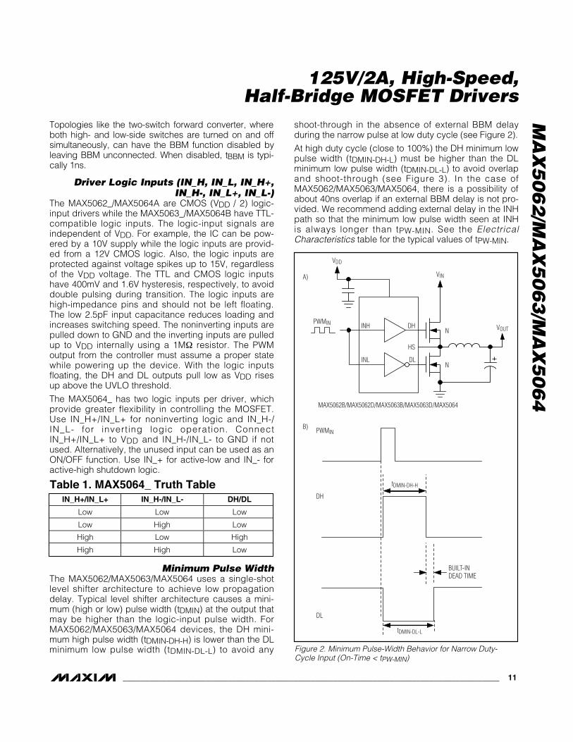
shoot-through in the absence of external BBM delayduring the narrow pulse at low duty cycle (see Figure 2).
At high duty cycle (close to 100%) the DH minimum lowpulse width (tDMIN-DH-L) must be higher than the DLminimum low pulse width (tDMIN-DL-L) to avoid overlapand shoot-through (see Figure 3). In the case ofMAX5062/MAX5063/MAX5064, there is a possibility ofabout 40ns overlap if an external BBM delay is not pro-vided. We recommend adding external delay in the INHpath so that the minimum low pulse width seen at INHis always longer than tPW-MIN. See the ElectricalCharacteristics table for the typical values of tPW-MIN.
MA
X5
06
2/M
AX
50
63
/MA
X5
06
4
125V/2A, High-Speed, Half-Bridge MOSFET Drivers
______________________________________________________________________________________ 11
IN_H+/IN_L+ IN_H-/IN_L- DH/DL
Low Low Low
Low High Low
High Low High
High High Low
Figure 2. Minimum Pulse-Width Behavior for Narrow Duty-Cycle Input (On-Time < tPW-MIN)
N
N
PWMIN
PWMIN
VDD
VIN
VOUTINH
INL
DH
DL
HS
DH
DL
tDMIN-DL-L
tDMIN-DH-H
BUILT-INDEAD TIME
MAX5062B/MAX5062D/MAX5063B/MAX5063D/MAX5064
A)
B)
Table 1. MAX5064_ Truth Table

MA
X5
06
2/M
AX
50
63
/MA
X5
06
4
Applications InformationSupply Bypassing and Grounding
Pay extra attention to bypassing and grounding theMAX5062/MAX5063/MAX5064. Peak supply and outputcurrents may exceed 4A when both drivers are drivinglarge external capacitive loads in-phase. Supply dropsand ground shifts create forms of negative feedback forinverters and may degrade the delay and transitiontimes. Ground shifts due to insufficient device ground-ing may also disturb other circuits sharing the same ACground return path. Any series inductance in the VDD,DH, DL, and/or GND paths can cause oscillations dueto the very high di/dt when switching the MAX5062/MAX5063/MAX5064 with any capacitive load. Placeone or more 0.1µF ceramic capacitors in parallel asclose to the device as possible to bypass VDD to GND(MAX5062/MAX5063) or PGND (MAX5064). Use aground plane to minimize ground return resistance and
series inductance. Place the external MOSFET as closeas possible to the MAX5062/MAX5063/MAX5064 to fur-ther minimize board inductance and AC path resis-tance. For the MAX5064_ the low-power logic ground(AGND) is separated from the high-power driver return(PGND). Apply the logic-input signal between IN_ toAGND and connect the load (MOSFET gate) betweenDL and PGND.
Power DissipationPower dissipation in the MAX5062/MAX5063/MAX5064is primarily due to power loss in the internal boostdiode and the nMOS and pMOS FETS.
For capacitive loads, the total power dissipation for thedevice is:
P C V f I I VD L DD SW DDO BSTO DD= × ×⎛⎝
⎞⎠ + +( ) ×2
125V/2A, High-Speed, Half-Bridge MOSFET Drivers
12 ______________________________________________________________________________________
Figure 3. Minimum Pulse-Width Behavior for High Duty-Cycle Input (Off-Time < tPW-MIN)
PWMIN
DH
DL
EXTERNALBBM DELAY
tDMIN-DH-L
POTENTIALOVERLAP TIME
tDMIN-DL-H
MAX5062B/MAX5062D/MAX5063B/MAX5063D/MAX5064
MAX5062A/MAX5062C/MAX5063A/MAX5063C/MAX5064
EXTERNALBBM DELAY
A)
B)
C)
N
N
PWMIN
VIN
VOUTINH
INL
DH
DL
HS
EXTERNALBBM DELAY
N
N
PWMIN
VIN
VDD
VDD
VOUTINH
INL
DH
DL
HS

MA
X5
06
2/M
AX
50
63
/MA
X5
06
4
125V/2A, High-Speed, Half-Bridge MOSFET Drivers
______________________________________________________________________________________ 13
where CL is the combined capacitive load at DH andDL. VDD is the supply voltage and fSW is the switchingfrequency of the converter. PD includes the power dis-sipated in the internal bootstrap diode. The internalpower dissipation reduces by PDIODE, if an externalbootstrap Schottky diode is used. The power dissipa-tion in the internal boost diode (when driving a capaci-tive load) will be the charge through the diode perswitching period multiplied by the maximum diode for-ward voltage drop (Vf = 1V).
The total power dissipation when using the internalboost diode will be PD and, when using an externalSchottky diode, will be PD - PDIODE. The total powerdissipated in the device must be kept below the maxi-mum of 1.951W for the 12-pin TQFN package, 1.5W forthe 8-pin SO with exposed pad, and 0.471W for theregular 8-pin SO package at TA = +70°C ambient.
Layout InformationThe MAX5062/MAX5063/MAX5064 drivers source andsink large currents to create very fast rise and falledges at the gates of the switching MOSFETs. The highdi/dt can cause unacceptable ringing if the tracelengths and impedances are not well controlled. Usethe following PC board layout guidelines when design-ing with the MAX5062/MAX5063/MAX5064:
• It is important that the VDD voltage (with respect toground) or BST voltage (with respect to HS) doesnot exceed 13.2V. Voltage spikes higher than 13.2V
from VDD to GND or BST to HS can damage thedevice. Place one or more low ESL 0.1µF decou-pling ceramic capacitors from VDD to GND(MAX5062/MAX5063) or to PGND (MAX5064), andfrom BST to HS as close as possible to the part. Theceramic decoupling capacitors should be at least20 times the gate capacitance being driven.
• There are two AC current loops formed between thedevice and the gate of the MOSFET being driven.The MOSFET looks like a large capacitance from gateto source when the gate is being pulled low. Theactive current loop is from the MOSFET driver output(DL or DH) to the MOSFET gate, to the MOSFETsource, and to the return terminal of the MOSFET dri-ver (either GND or HS). When the gate of the MOS-FET is being pulled high, the active current loop isfrom the MOSFET driver output, (DL or DH), to theMOSFET gate, to the MOSFET source, to the returnterminal of the drivers decoupling capacitor, to thepositive terminal of the decoupling capacitor, and tothe supply connection of the MOSFET driver. Thedecoupling capacitor will be either the flying capaci-tor connected between BST and HS or the decou-pling capacitor for VDD. Care must be taken tominimize the physical distance and the impedance ofthese AC current paths.
• Solder the exposed pad of the TQFN (MAX5064) orSO (MAX5062C/D and MAX5063C/D) package to alarge copper plane to achieve the rated power dissi-pation. Connect AGND and PGND at one point nearVDD’s decoupling capacitor return.
P C V f VDIODE DH DD SW f= × ( ) × ×− 1

MA
X5
06
2/M
AX
50
63
/MA
X5
06
4
125V/2A, High-Speed, Half-Bridge MOSFET Drivers
14 ______________________________________________________________________________________
Typical Application Circuits
Figure 4. MAX5062 Half-Bridge Conversion
MAX5062A/MAX5063A
VOUT
N
N
VDD = 8V TO 12.6V VIN = 0 TO 125V
VDD BST
IN_H
IN_L
GND
DL
DH
HS
PWMCONTROLLER
PIN FOR PIN REPLACEMENT FOR THE HIP2100/HIP2101
Figure 5. Synchronous Buck Converter
MAX5064N
N
VDD = 8V TO 12.6V VIN = 0 TO 125V
VOUT
VDD BST
IN_H+
IN_L-
BBM
AGND PGND
DL
DH
HS
RBBM
PWM
CBBM
CBST

MA
X5
06
2/M
AX
50
63
/MA
X5
06
4
125V/2A, High-Speed, Half-Bridge MOSFET Drivers
______________________________________________________________________________________ 15
Typical Application Circuits (continued)
Figure 6. Two-Switch Forward Conversion
MAX5064N
N
VDD = 8V TO 12.6V VIN = 0 TO 125V
VOUT
VDD BST
IN_H+
IN_L+
BBM
AGND PGND
DL
DH
HSPWM
CBST
Figure 7. MAX5064 Half-Bridge Converter
MAX5064_
VOUT
N
N
VDD = 8V TO 12.6V VIN = 0 TO 125V
VDD BST
IN_H+
IN_L-
BBM
PGNDAGND
DL
DH
HS
RBBM
PWM
CBBM
CBST

MA
X5
06
2/M
AX
50
63
/MA
X5
06
4
125V/2A, High-Speed, Half-Bridge MOSFET Drivers
16 ______________________________________________________________________________________
IN_L
IN_HHS
1
2
8
7
DL
GNDBST
DH
VDD
SO
TOP VIEW
3
4
6
5
MAX5062A/BMAX5063A/B IN_L
IN_HHS
1
2
8
7
DL
GNDBST
DH
VDD
SO-EP
3
4
6
5
MAX5062C/DMAX5063C/D
9
IN_L+
8
IN_L-
7
IN_H+
1 2
DH
3
HS
10
11DL
12
6
5
4VDD
IN_H-
BBM
AGND
MAX5064A/MAX5064B
PGND
BST
THIN QFN
Pin Configurations
MAX5062AMAX5062C
GND
VDD
IN_H DH
DL
HS
BST
IN_L
2
3
4
5
8
7
6
1
VDD/2 CMOS
MAX5064A
PGND
VDD
IN_H+
IN_L-
DH
DL
HS
BST
BBM
IN_H-
IN_L+
AGND
1
2
4
3
7
8
56
11
10
912
VDD/2 CMOS
MAX5064B
PGND
VDD
IN_H+
IN_L-
DH
DL
HS
BST
BBM
IN_H-
IN_L+
AGND
1
2
4
3
7
8
56
11
10
912
TTL
SO/SO-EP
MAX5062B/MAX5062D
GND
VDD
IN_H DH
DL
HS
BST
IN_L
2
3
4
5
8
7
6
1
VDD/2 CMOS
SO/SO-EP
MAX5063B/MAX5063D
GND
VDD
IN_H DH
DL
HS
BST
IN_L
2
3
4
5
8
7
6
1
TTL
SO/SO-EP
MAX5063A/MAX5063C
GND
VDD
IN_H DH
DL
HS
BST
IN_L
2
3
4
5
8
7
6
1
TTL
SO/SO-EP
THIN QFN THIN QFN
Functional Diagrams

MA
X5
06
2/M
AX
50
63
/MA
X5
06
4
125V/2A, High-Speed, Half-Bridge MOSFET Drivers
______________________________________________________________________________________ 17
MAX5064A/MAX5064B
PWM IN
VOUT
PGND
IN_H+
IN_L-
DH
DL
HS
BST
BBM
VDD
IN_L+
IN_H-
RBBM
AGNDCBBM
VDD
CBST
CDD
VIN = 125V
VDD8V TO 12.6V
Typical Operating Circuit
PARTTEMP
RANGEPIN-PACKAGE
TOPMARK
PKG CODE
MAX5063AASA-40°C to+125°C
8 SO — S8-5
MAX5063BASA-40°C to+125°C
8 SO — S8-5
MAX5063CASA-40°C to+125°C
8 SO-EP* — S8E-14
MAX5063DASA-40°C to+125°C
8 SO-EP* — S8E-14
MAX5064AATC-40°C to+125°C
12 TQFN AAEF T1244-4
MAX5064BATC-40°C to+125°C
12 TQFN AAEG T1244-4
Ordering Information (continued)
PART HIGH-SIDE DRIVER LOW-SIDE DRIVER LOGIC LEVELS PIN COMPATIBLE
MAX5063AASA Noninverting Noninverting TTL HIP2101IB
MAX5063BASA Noninverting Inverting TTL —
MAX5063CASA Noninverting Noninverting TTL —MAX5063DASA Noninverting Inverting TTL —
MAX5064AATCBoth Inverting and
NoninvertingBoth Inverting and
NoninvertingCMOS (VDD / 2) —
MAX5064BATCBoth Inverting and
NoninvertingBoth Inverting and
NoninvertingTTL —
Selector Guide (continued)
Chip InformationTRANSISTOR COUNT: 790
PROCESS: HV BiCMOS
*EP = Exposed paddle.Devices are available in both leaded and lead-free packaging.Specify lead-free by replacing “-T” with “+T” when ordering.

MA
X5
06
2/M
AX
50
63
/MA
X5
06
4
125V/2A, High-Speed, Half-Bridge MOSFET Drivers
18 ______________________________________________________________________________________
Package Information(The package drawing(s) in this data sheet may not reflect the most current specifications. For the latest package outline informationgo to www.maxim-ic.com/packages.)
8L, S
OIC
EX
P. P
AD
.EP
S
C 1121-0111
PACKAGE OUTLINE8L SOIC, .150" EXPOSED PAD

MA
X5
06
2/M
AX
50
63
/MA
X5
06
4
125V/2A, High-Speed, Half-Bridge MOSFET Drivers
______________________________________________________________________________________ 19
Package Information (continued)(The package drawing(s) in this data sheet may not reflect the most current specifications. For the latest package outline informationgo to www.maxim-ic.com/packages.)
24L
QFN
TH
IN.E
PS

MA
X5
06
2/M
AX
50
63
/MA
X5
06
4
125V/2A, High-Speed, Half-Bridge MOSFET Drivers
Maxim cannot assume responsibility for use of any circuitry other than circuitry entirely embodied in a Maxim product. No circuit patent licenses areimplied. Maxim reserves the right to change the circuitry and specifications without notice at any time.
20 ____________________Maxim Integrated Products, 120 San Gabriel Drive, Sunnyvale, CA 94086 408-737-7600
© 2007 Maxim Integrated Products is a registered trademark of Maxim Integrated Products, Inc.
Package Information (continued)(The package drawing(s) in this data sheet may not reflect the most current specifications. For the latest package outline informationgo to www.maxim-ic.com/packages.)
Revision HistoryPages changed at Rev 5: 1, 2, 4, 5, 11–15, 19, 20