12×12 DOTS MATRIX LED DRIVER WITH INDIVIDUAL AUTO BREATH ... · IS31FL3737 Integrated Silicon...
28
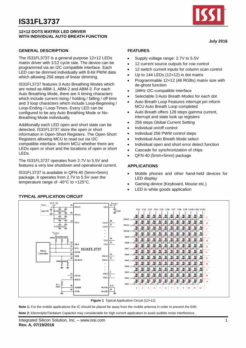
IS31FL3737 Integrated Silicon Solution, Inc. – www.issi.com 1 Rev. A, 07/19/2016 12×12 DOTS MATRIX LED DRIVER WITH INDIVIDUAL AUTO BREATH FUNCTION July 2016 GENERAL DESCRIPTION The IS31FL3737 is a general purpose 12×12 LEDs matrix driver with 1/12 cycle rate. The device can be programmed via an I2C compatible interface. Each LED can be dimmed individually with 8-bit PWM data which allowing 256 steps of linear dimming. IS31FL3737 features 3 Auto Breathing Modes which are noted as ABM-1, ABM-2 and ABM-3. For each Auto Breathing Mode, there are 4 timing characters which include current rising / holding / falling / off time and 3 loop characters which include Loop-Beginning / Loop-Ending / Loop-Times. Every LED can be configured to be any Auto Breathing Mode or No- Breathing Mode individually. Additionally each LED open and short state can be detected, IS31FL3737 store the open or short information in Open-Short Registers. The Open-Short Registers allowing MCU to read out via I2C compatible interface. Inform MCU whether there are LEDs open or short and the locations of open or short LEDs. The IS31FL3737 operates from 2.7V to 5.5V and features a very low shutdown and operational current. IS31FL3737 is available in QFN-40 (5mm×5mm) package. It operates from 2.7V to 5.5V over the temperature range of -40°C to +125°C. FEATURES Supply voltage range: 2.7V to 5.5V 12 current source outputs for row control 12 switch current inputs for column scan control Up to 144 LEDs (12×12) in dot matrix Programmable 12×12 (48 RGBs) matrix size with de-ghost function 1MHz I2C-compatible interface Selectable 3 Auto Breath Modes for each dot Auto Breath Loop Features interrupt pin inform MCU Auto Breath Loop completed Auto Breath offers 128 steps gamma current, interrupt and state look up registers 256 steps Global Current Setting Individual on/off control Individual 256 PWM control steps Individual Auto Breath Mode select Individual open and short error detect function Cascade for synchronization of chips QFN-40 (5mm×5mm) package APPLICATIONS Mobile phones and other hand-held devices for LED display Gaming device (Keyboard, Mouse etc.) LED in white goods application TYPICAL APPLICATION CIRCUIT CS1 CS2 CS3 CS4 CS5 CS6 CS7 CS8 CS9 CS10 CS11 CS12 SDA SCL IICRST IS31FL3737 4.7kΩ 4.7kΩ V IO/MCU 100kΩ INTB REXT 20kΩ RSET 100kΩ SYNC GND ADDR SW1 SW2 CS12 CS11 CS2 CS1 SW11 SW12 SDB 100kΩ SW12 SW2 SW9 SW10 SW4 SW5 SW11 SW6 SW7 SW3 SW8 SW1 1 2 3 4 5 6 7 8 9 10 11 12 Micro Controller 34 35 37 38 39 33 30 36 40 28 27 16 15 14 13 2 1 PGND 4,11 AGND 29 VIO V IO/MCU 0.47μF 32 PVCC VCC 0.47μF 0.1μF 26 31 0.47μF 0.1μF VCC_5V PVCC 0.47μF 0.1μF 19 A B C D E F G H I J K L 22μF/10V *Note2 Figure 1 Typical Application Circuit (12×12) Note 1: For the mobile applications the IC should be placed far away from the mobile antenna in order to prevent the EMI. Note 2: Electrolytic/Tantalum Capacitor may considerable for high current application to avoid audible noise interference.
Transcript of 12×12 DOTS MATRIX LED DRIVER WITH INDIVIDUAL AUTO BREATH ... · IS31FL3737 Integrated Silicon...
IS31FL3737
Integrated Silicon Solution, Inc. – www.issi.com 1 Rev. A, 07/19/2016
12×12 DOTS MATRIX LED DRIVER WITH INDIVIDUAL AUTO BREATH FUNCTION
July 2016
GENERAL DESCRIPTION
The IS31FL3737 is a general purpose 12×12 LEDs matrix driver with 1/12 cycle rate. The device can be programmed via an I2C compatible interface. Each LED can be dimmed individually with 8-bit PWM data which allowing 256 steps of linear dimming.
IS31FL3737 features 3 Auto Breathing Modes which are noted as ABM-1, ABM-2 and ABM-3. For each Auto Breathing Mode, there are 4 timing characters which include current rising / holding / falling / off time and 3 loop characters which include Loop-Beginning / Loop-Ending / Loop-Times. Every LED can be configured to be any Auto Breathing Mode or No-Breathing Mode individually.
Additionally each LED open and short state can be detected, IS31FL3737 store the open or short information in Open-Short Registers. The Open-Short Registers allowing MCU to read out via I2C compatible interface. Inform MCU whether there are LEDs open or short and the locations of open or short LEDs.
The IS31FL3737 operates from 2.7V to 5.5V and features a very low shutdown and operational current.
IS31FL3737 is available in QFN-40 (5mm×5mm) package. It operates from 2.7V to 5.5V over the temperature range of -40°C to +125°C.
FEATURES
Supply voltage range: 2.7V to 5.5V
12 current source outputs for row control
12 switch current inputs for column scan control
Up to 144 LEDs (12×12) in dot matrix
Programmable 12×12 (48 RGBs) matrix size with de-ghost function
1MHz I2C-compatible interface
Selectable 3 Auto Breath Modes for each dot
Auto Breath Loop Features interrupt pin inform MCU Auto Breath Loop completed
Auto Breath offers 128 steps gamma current, interrupt and state look up registers
256 steps Global Current Setting
Individual on/off control
Individual 256 PWM control steps
Individual Auto Breath Mode select
Individual open and short error detect function
Cascade for synchronization of chips
QFN-40 (5mm×5mm) package
APPLICATIONS
Mobile phones and other hand-held devices for LED display
Gaming device (Keyboard, Mouse etc.)
LED in white goods application
TYPICAL APPLICATION CIRCUIT
CS1 CS2 CS3 CS4 CS5 CS6 CS7 CS8 CS9 CS10 CS11 CS12
SDA
SCL
IICRST
IS31FL3737
4.7kΩ4.7kΩ
VIO/MCU
100kΩ
INTB
REXT
20kΩ
RSET
100kΩ
SYNC
GND
ADDR
SW1
SW2
CS12
CS11
CS2
CS1
SW11
SW12SDB
100kΩ
SW12
SW2
SW9
SW10
SW4
SW5
SW11
SW6
SW7
SW3
SW8
SW1
1 2 3 4 5 6 7 8 9 10 11 12
Micro
Controller
34
35
37
38
39
33
30
36
40
28
27
16
15
14
13
2
1
PGND4,11
AGND29
VIO
VIO/MCU
0.47μF
32
PVCC
VCC
0.47μF 0.1μF
26
31
0.47μF 0.1μF
VCC_5V
PVCC
0.47μF 0.1μF
19
A
B
C
D
E
F
G
H
I
J
K
L
22μF/10V
*Note2
Figure 1 Typical Application Circuit (12×12)
Note 1: For the mobile applications the IC should be placed far away from the mobile antenna in order to prevent the EMI.
Note 2: Electrolytic/Tantalum Capacitor may considerable for high current application to avoid audible noise interference.
IS31FL3737
Integrated Silicon Solution, Inc. – www.issi.com 2 Rev. A, 07/19/2016
TYPICAL APPLICATION CIRCUIT (CONTINUED)
CS1 CS2 CS3 CS4 CS5 CS6 CS7 CS8 CS9 CS10 CS11 CS12
SDA
SCL
IICRST
IS31FL3737
4.7kΩ4.7kΩ
VIO/MCU
100kΩ
INTB
REXT
20kΩ
RSET
100kΩ
SYNC
GND
ADDR
SW1
SW2
CS12
CS11
CS2
CS1
SW11
SW12SDB
100kΩ
SW12
SW2
SW9
SW10
SW4
SW5
SW11
SW6
SW7
SW3
SW8
SW1
1 2 3 4 5 6 7 8 9 10 11 12
Micro
Controller
34
35
37
38
39
33
30
36
40
28
27
16
15
14
13
2
1
PGND4,11
AGND29
VIO
VIO/MCU
0.47μF
32
PVCC
VCC
0.47μF 0.1μF
26
31
0.47μF 0.1μF
VCC_5V
PVCC
0.47μF 0.1μF
19
A
B
C
D
E
F
G
H
I
J
K
L
22μF/10V
*Note4
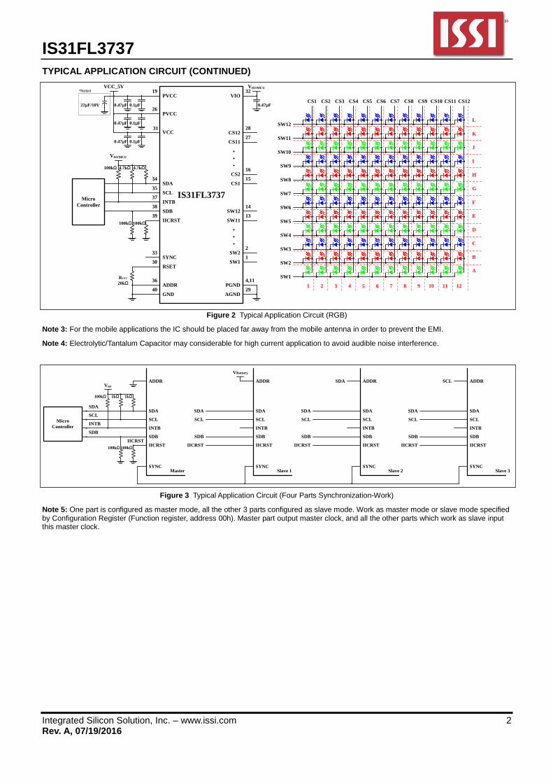
Figure 2 Typical Application Circuit (RGB)
Note 3: For the mobile applications the IC should be placed far away from the mobile antenna in order to prevent the EMI.
Note 4: Electrolytic/Tantalum Capacitor may considerable for high current application to avoid audible noise interference.
SDA
SCL
1kΩ1kΩ
VIO
100kΩ
INTB
100kΩ
SYNC
Micro
Controller
SDA
SCL
SDB
INTB
SYNC
SDA
SCL
SDB
SDA
SCL
SDB
INTB
SDA
SCL
SDB
INTB
SYNC
SDA
SCL
SDB
SDA
SCL
SDB
INTB
SYNC
SDA
SCL
SDB
ADDR ADDR
VBattery
ADDRSDA ADDRSCL
Master Slave 1 Slave 2 Slave 3
SDB
IICRST100kΩ
IICRSTIICRST IICRSTIICRST IICRSTIICRSTIICRST
Figure 3 Typical Application Circuit (Four Parts Synchronization-Work)
Note 5: One part is configured as master mode, all the other 3 parts configured as slave mode. Work as master mode or slave mode specified by Configuration Register (Function register, address 00h). Master part output master clock, and all the other parts which work as slave input this master clock.
IS31FL3737
Integrated Silicon Solution, Inc. – www.issi.com 3 Rev. A, 07/19/2016
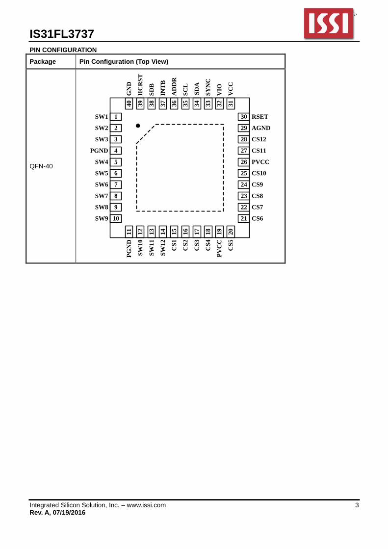
PIN CONFIGURATION
Package Pin Configuration (Top View)
QFN-40
1
2
3
4
34
23
27
33
32
31
13
15
16
19
5
20
21
6
11
22
7
14
243
5
25
26
8
9
17
18
36
37
10
12
30
28
29
38
39
40
SW
11
CS6
CS
1
CS
2
CS
3
PV
CC
CS
5
CS
4
SW
10
SW
12
CS8
AGND
RSET
CS11
CS12
CS9
CS10
PVCC
CS7
SD
B
IIC
RS
T
AD
DR
SD
A
SC
L
VIO
VC
C
GN
D
SY
NC
INT
B
SW6
SW1
SW2
SW5
PGND
SW4
SW7
SW8
SW9
PG
ND
SW3
IS31FL3737
Integrated Silicon Solution, Inc. – www.issi.com 4 Rev. A, 07/19/2016
PIN DESCRIPTION
No. Pin Description
1~3,5~10, 12~14
SW1~SW12 Switch pin for LED matrix scanning.
4,11 PGND Power GND.
15~18,20~25,27,28
CS1~CS12 Current Source.
19,26 PVCC Power for current source.
29 AGND Analog GND.
30 RSET Input terminal used to connect an external resistor. This regulates current source DC current value.
31 VCC Power for analog and digital circuits.
32 VIO Input logic reference voltage.
33 SYNC Synchronize pin. It is used for more than one part work synchronize. If it is not used please float this pin.
34 SDA I2C compatible serial data.
35 SCL I2C compatible serial clock.
36 ADDR I2C address setting.
37 INTB
Interrupt output pin. Register F0h sets the function of the INTB pin and active low when the interrupt event happens. Can be NC (float) if interrupt function no used.
38 SDB Shutdown the chip when pull to low.
39 IICRST Reset I2C when pull high, need to pull down when normal operation.
40 GND Connect to GND.
Thermal Pad Need to connect to GND pins.
IS31FL3737
Integrated Silicon Solution, Inc. – www.issi.com 5 Rev. A, 07/19/2016
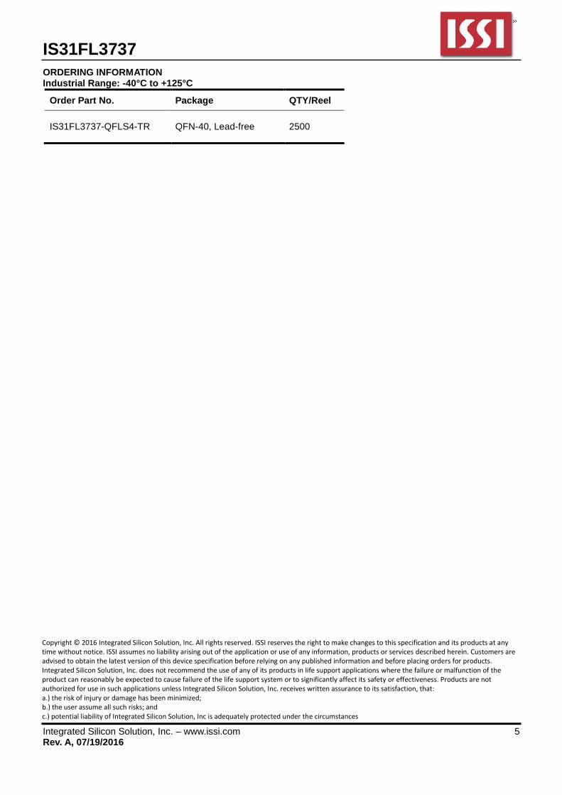
ORDERING INFORMATION Industrial Range: -40°C to +125°C
Order Part No. Package QTY/Reel
IS31FL3737-QFLS4-TR QFN-40, Lead-free 2500
Copyright © 2016 Integrated Silicon Solution, Inc. All rights reserved. ISSI reserves the right to make changes to this specification and its products at any time without notice. ISSI assumes no liability arising out of the application or use of any information, products or services described herein. Customers are advised to obtain the latest version of this device specification before relying on any published information and before placing orders for products. Integrated Silicon Solution, Inc. does not recommend the use of any of its products in life support applications where the failure or malfunction of the product can reasonably be expected to cause failure of the life support system or to significantly affect its safety or effectiveness. Products are not authorized for use in such applications unless Integrated Silicon Solution, Inc. receives written assurance to its satisfaction, that: a.) the risk of injury or damage has been minimized; b.) the user assume all such risks; and c.) potential liability of Integrated Silicon Solution, Inc is adequately protected under the circumstances
IS31FL3737
Integrated Silicon Solution, Inc. – www.issi.com 6 Rev. A, 07/19/2016
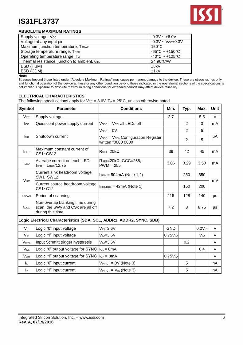
ABSOLUTE MAXIMUM RATINGS
Supply voltage, VCC -0.3V ~ +6.0V
Voltage at any input pin -0.3V ~ VCC+0.3V
Maximum junction temperature, TJMAX 150°C
Storage temperature range, TSTG -65°C ~ +150°C
Operating temperature range, TA -40°C ~ +125°C
Thermal resistance, junction to ambient, θJA 24.96°C/W
ESD (HBM) ESD (CDM)
±8kV ±1kV
Note: Stresses beyond those listed under “Absolute Maximum Ratings” may cause permanent damage to the device. These are stress ratings only and functional operation of the device at these or any other condition beyond those indicated in the operational sections of the specifications is not implied. Exposure to absolute maximum rating conditions for extended periods may affect device reliability.
ELECTRICAL CHARACTERISTICS The following specifications apply for VCC = 3.6V, TA = 25°C, unless otherwise noted.
Symbol Parameter Conditions Min. Typ. Max. Unit
VCC Supply voltage 2.7 5.5 V
ICC Quiescent power supply current VSDB = VCC, all LEDs off 2 3 mA
ISD Shutdown current
VSDB = 0V 2 5
μA VSDB = VCC, Configuration Register written “0000 0000
2 5
IOUT Maximum constant current of CS1~CS12
RSET=20kΩ 39 42 45 mA
ILED Average current on each LED ILED = LOUT/12.75
RSET=20kΩ, GCC=255, PWM = 255
3.06 3.29 3.53 mA
VHR
Current sink headroom voltage SW1~SW12
ISINK = 504mA (Note 1,2) 250 350
mV Current source headroom voltage CS1~C12
ISOURCE = 42mA (Note 1) 150 200
tSCAN Period of scanning 115 128 140 µs
tNOL Non-overlap blanking time during scan, the SWy and CSx are all off during this time
7.2 8 8.75 µs
Logic Electrical Characteristics (SDA, SCL, ADDR1, ADDR2, SYNC, SDB)
VIL Logic “0” input voltage VIO=3.6V GND 0.2VIO V
VIH Logic “1” input voltage VIO=3.6V 0.75VIO VIO V
VHYS Input Schmitt trigger hysteresis VIO=3.6V 0.2 V
VOL Logic “0” output voltage for SYNC IOL = 8mA 0.4 V
VOH Logic “1” output voltage for SYNC IOH = 8mA 0.75VIO V
IIL Logic “0” input current VINPUT = 0V (Note 3) 5 nA
IIH Logic “1” input current VINPUT = VIO (Note 3) 5 nA
IS31FL3737
Integrated Silicon Solution, Inc. – www.issi.com 7 Rev. A, 07/19/2016
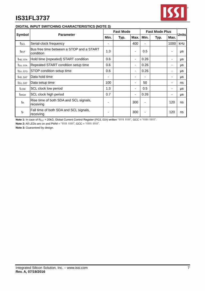
DIGITAL INPUT SWITCHING CHARACTERISTICS (NOTE 3)
Symbol Parameter Fast Mode Fast Mode Plus
Units Min. Typ. Max. Min. Typ. Max.
fSCL Serial-clock frequency - 400 - 1000 kHz
tBUF Bus free time between a STOP and a START condition
1.3 - 0.5 - μs
tHD, STA Hold time (repeated) START condition 0.6 - 0.26 - μs
tSU, STA Repeated START condition setup time 0.6 - 0.26 - μs
tSU, STO STOP condition setup time 0.6 - 0.26 - μs
tHD, DAT Data hold time - - - - μs
tSU, DAT Data setup time 100 - 50 - ns
tLOW SCL clock low period 1.3 - 0.5 - μs
tHIGH SCL clock high period 0.7 - 0.26 - μs
tR Rise time of both SDA and SCL signals, receiving
- 300 - 120 ns
tF Fall time of both SDA and SCL signals, receiving
- 300 - 120 ns
Note 1: In case of REXT = 20kΩ, Global Current Control Register (PG3, 01h) written “1111 1111”, GCC = “1111 1111”.
Note 2: All LEDs are on and PWM = “1111 1111”, GCC = “1111 1111”.
Note 3: Guaranteed by design.
IS31FL3737
Integrated Silicon Solution, Inc. – www.issi.com 8 Rev. A, 07/19/2016
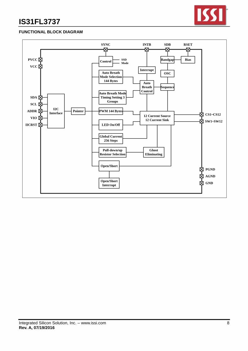
FUNCTIONAL BLOCK DIAGRAM
Pointer
SDA
SCL
I2C
Interface CS1~CS12
PGND
PVCC
SYNC
Control
Auto Breath
Mode Selection
144 Bytes
Auto Breath Mode
Timing Setting 3
Groups
PWM 144 Bytes
LED On/Off
Global Current
256 Steps
Pull-down/up
Resistor Selection
Open/Short
Open/Short
Interrupt
Auto
Breath
Control
Interrupt
SSD
Mode
12 Current Source
12 Current Sink
Ghost
Eliminating
Sequence
OSC
Bandgap Bias
VCC
ADDR
VIO
INTB SDB RSET
SW1~SW12
AGND
GND
IICRST
IS31FL3737
Integrated Silicon Solution, Inc. – www.issi.com 9 Rev. A, 07/19/2016
DETAILED DESCRIPTION
I2C INTERFACE
The IS31FL3737 uses a serial bus, which conforms to the I2C protocol, to control the chip’s functions with two wires: SCL and SDA. The IS31FL3737 has a 7-bit slave address (A7:A1), followed by the R/W bit, A0. Set A0 to “0” for a write command and set A0 to “1” for a read command. The value of bits A4:A1 are decided by the connection of the ADDR pin.
The complete slave address is:
Table 1 Slave Address:
ADDR A7:A5 A4:A1 A0
GND
101
0000
0/1 SCL 0101
SDA 1010
VCC 1111
ADDR connected to GND, (A4:A1)= 0000;
ADDR connected to VCC, (A4:A1)= 1111;
ADDR connected to SCL, (A4:A1)= 0101;
ADDR connected to SDA, (A4:A1)= 1010;
The SCL line is uni-directional. The SDA line is bi-directional (open-collector) with a pull-up resistor (typically 1kΩ). The maximum clock frequency specified by the I2C standard is 1MHz. In this discussion, the master is the microcontroller and the slave is the IS31FL3737.
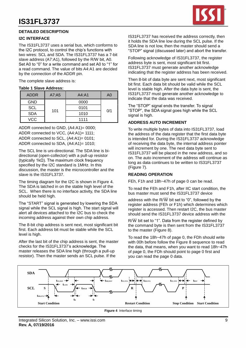
The timing diagram for the I2C is shown in Figure 4. The SDA is latched in on the stable high level of the SCL. When there is no interface activity, the SDA line should be held high.
The “START” signal is generated by lowering the SDA signal while the SCL signal is high. The start signal will alert all devices attached to the I2C bus to check the incoming address against their own chip address.
The 8-bit chip address is sent next, most significant bit first. Each address bit must be stable while the SCL level is high.
After the last bit of the chip address is sent, the master checks for the IS31FL3737’s acknowledge. The master releases the SDA line high (through a pull-up resistor). Then the master sends an SCL pulse. If the
IS31FL3737 has received the address correctly, then it holds the SDA line low during the SCL pulse. If the SDA line is not low, then the master should send a “STOP” signal (discussed later) and abort the transfer.
Following acknowledge of IS31FL3737, the register address byte is sent, most significant bit first. IS31FL3737 must generate another acknowledge indicating that the register address has been received.
Then 8-bit of data byte are sent next, most significant bit first. Each data bit should be valid while the SCL level is stable high. After the data byte is sent, the IS31FL3737 must generate another acknowledge to indicate that the data was received.
The “STOP” signal ends the transfer. To signal “STOP”, the SDA signal goes high while the SCL signal is high.
ADDRESS AUTO INCREMENT
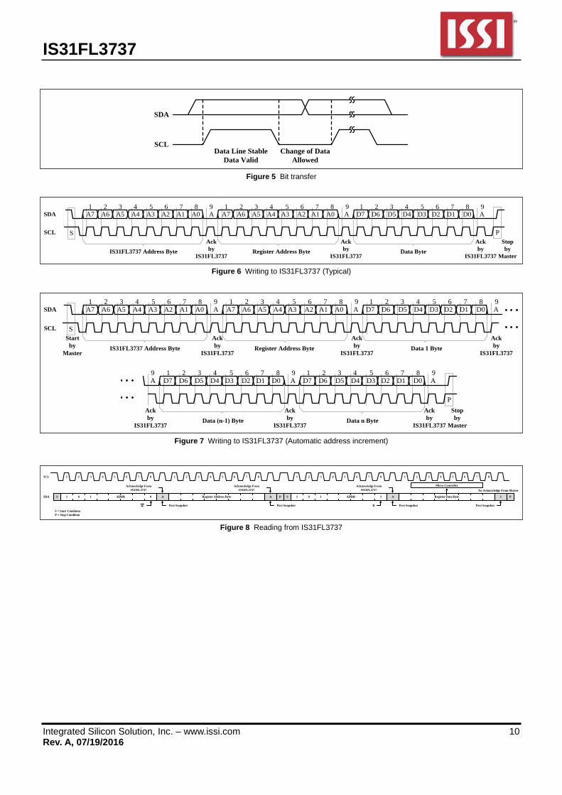
To write multiple bytes of data into IS31FL3737, load the address of the data register that the first data byte is intended for. During the IS31FL3737 acknowledge of receiving the data byte, the internal address pointer will increment by one. The next data byte sent to IS31FL3737 will be placed in the new address, and so on. The auto increment of the address will continue as long as data continues to be written to IS31FL3737 (Figure 7).
READING OPERATION
FEh, F1h and 18h~47h of page 0 can be read.
To read the FEh and F1h, after IIC start condition, the bus master must send the IS31FL3737 device
address with the R/W____
bit set to “0”, followed by the register address (FEh or F1h) which determines which register is accessed. Then restart I2C, the bus master should send the IS31FL3737 device address with the
R/W____
bit set to “1”. Data from the register defined by the command byte is then sent from the IS31FL3737 to the master (Figure 8).
To read the 18h~47h of page 0, the FDh should write with 00h before follow the Figure 8 sequence to read the data, that means, when you want to read 18h~47h of page 0, the FDh should point to page 0 first and you can read the page 0 data.
SDA
SCL
tHD,STA
tLOW
tHIGH
tSU,DAT tHD,DAT
tR tF
tSU,STA tHD,STA tSU,STO tBUF
S R P
Start Condition Restart Condition Stop Condition Start Condition
Figure 4 Interface timing
IS31FL3737
Integrated Silicon Solution, Inc. – www.issi.com 10 Rev. A, 07/19/2016
Data Line Stable
Data Valid
Change of Data
Allowed
SDA
SCL
Figure 5 Bit transfer
A7 A6 A5 A4 A3 A2 A1 A0 A A7 A6 A5 A4 A3 A2 A11 2 3 4 5 6 7 8 9 1 2 3 4 5 6 7 8 9
S
A0 A D7 D6 D5 D4 D3 D2 D11 2 3 4 5 6 7 8 9
D0 A
P
IS31FL3737 Address Byte Register Address Byte Data Byte
Ack
by
IS31FL3737
SDA
SCL
Ack
by
IS31FL3737
Ack
by
IS31FL3737
Stop
by
Master
Figure 6 Writing to IS31FL3737 (Typical)
Start
by
Master
A7 A6 A5 A4 A3 A2 A1 A0 A A7 A6 A5 A4 A3 A2 A11 2 3 4 5 6 7 8 9 1 2 3 4 5 6 7 8 9
S
A0 A D7 D6 D5 D4 D3 D2 D11 2 3 4 5 6 7 8 9
D0 A
IS31FL3737 Address Byte Register Address Byte Data 1 Byte
A D7 D6 D5 D4 D3 D2 D19 1 2 3 4 5 6 7 8 9
D0 A D7 D6 D5 D4 D3 D2 D11 2 3 4 5 6 7 8 9
D0 A
P
Data n ByteData (n-1) Byte
SDA
SCL
Ack
by
IS31FL3737
Ack
by
IS31FL3737
Ack
by
IS31FL3737
Ack
by
IS31FL3737
Stop
by
Master
Ack
by
IS31FL3737
Ack
by
IS31FL3737
Figure 7 Writing to IS31FL3737 (Automatic address increment)
A
1 P
PAS
S = Start Condition
P = Stop Condition
SCL 1 2 3 4 5 6 7 8 1 2 3 4 5 6 7 8
1 0 1 ADDR 0SDA Register Data Byte A
Port SnapshotW
Acknowledge From
IS31FL3737
Acknowledge From
IS31FL3737
Port Snapshot
Acknowledge From
IS31FL3737
Port Snapshot
1 2 3 4 5 6 7 8
AS
SCL 1 2 3 4 5 6 7 8 1 2 3 4 5 6 7 8
1 0 1 ADDR 0SDA Register Address Byte A A
Port SnapshotW
Acknowledge From
IS31FL3737
Acknowledge From
IS31FL3737
Port Snapshot
Acknowledge From
IS31FL3737
1 2 3 4 5 6 7 8
1 0 1 ADDR 1
Port SnapshotR
1 2 3 4 5 6 7 8
Register Data Byte
Micro Controller
Port Snapshot
No Acknowledge From Master
SP
Register Address Byte
Figure 8 Reading from IS31FL3737
IS31FL3737
Integrated Silicon Solution, Inc. – www.issi.com 11 Rev. A, 07/19/2016
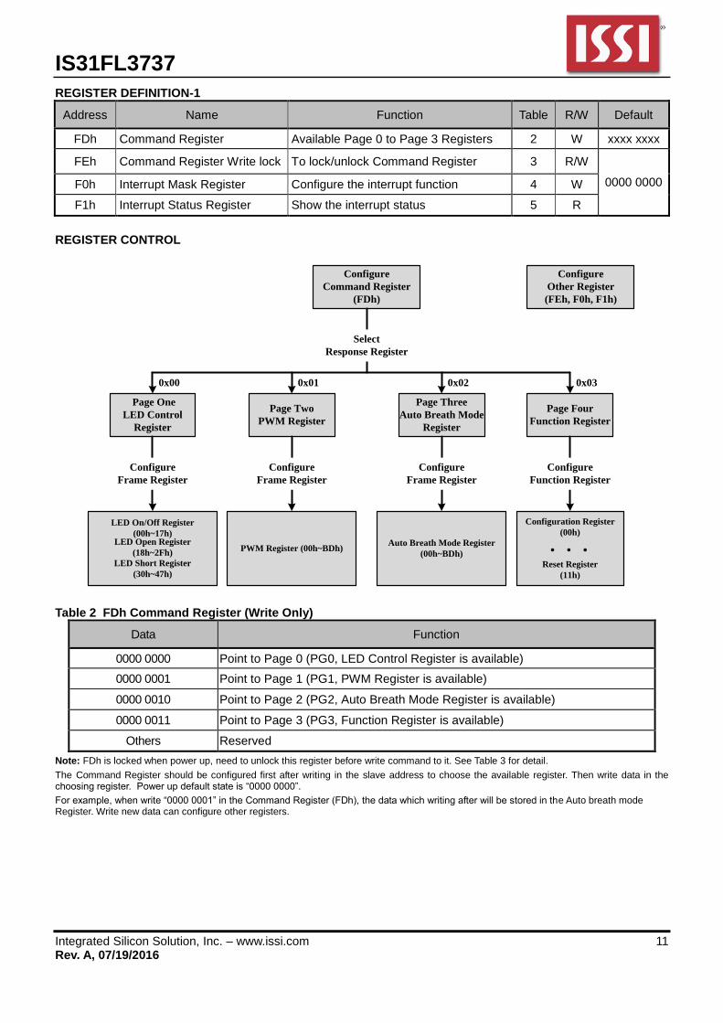
REGISTER DEFINITION-1
Address Name Function Table R/W Default
FDh Command Register Available Page 0 to Page 3 Registers 2 W xxxx xxxx
FEh Command Register Write lock To lock/unlock Command Register 3 R/W
0000 0000 F0h Interrupt Mask Register Configure the interrupt function 4 W
F1h Interrupt Status Register Show the interrupt status 5 R
REGISTER CONTROL
Configure
Command Register
(FDh)
0x03
Page One
LED Control
Register
LED On/Off Register
(00h~17h)
LED Short Register
(30h~47h)
LED Open Register
(18h~2Fh)
Configuration Register
(00h)
Reset Register
(11h)
0x00 0x01 0x02
Page Two
PWM Register
Page Three
Auto Breath Mode
Register
Page Four
Function Register
PWM Register (00h~BDh)Auto Breath Mode Register
(00h~BDh)
Select
Response Register
Configure
Frame Register
Configure
Frame Register
Configure
Frame Register
Configure
Function Register
Configure
Other Register
(FEh, F0h, F1h)
Table 2 FDh Command Register (Write Only)
Data Function
0000 0000 Point to Page 0 (PG0, LED Control Register is available)
0000 0001 Point to Page 1 (PG1, PWM Register is available)
0000 0010 Point to Page 2 (PG2, Auto Breath Mode Register is available)
0000 0011 Point to Page 3 (PG3, Function Register is available)
Others Reserved
Note: FDh is locked when power up, need to unlock this register before write command to it. See Table 3 for detail.
The Command Register should be configured first after writing in the slave address to choose the available register. Then write data in the choosing register. Power up default state is “0000 0000”.
For example, when write “0000 0001” in the Command Register (FDh), the data which writing after will be stored in the Auto breath mode Register. Write new data can configure other registers.
IS31FL3737
Integrated Silicon Solution, Inc. – www.issi.com 12 Rev. A, 07/19/2016
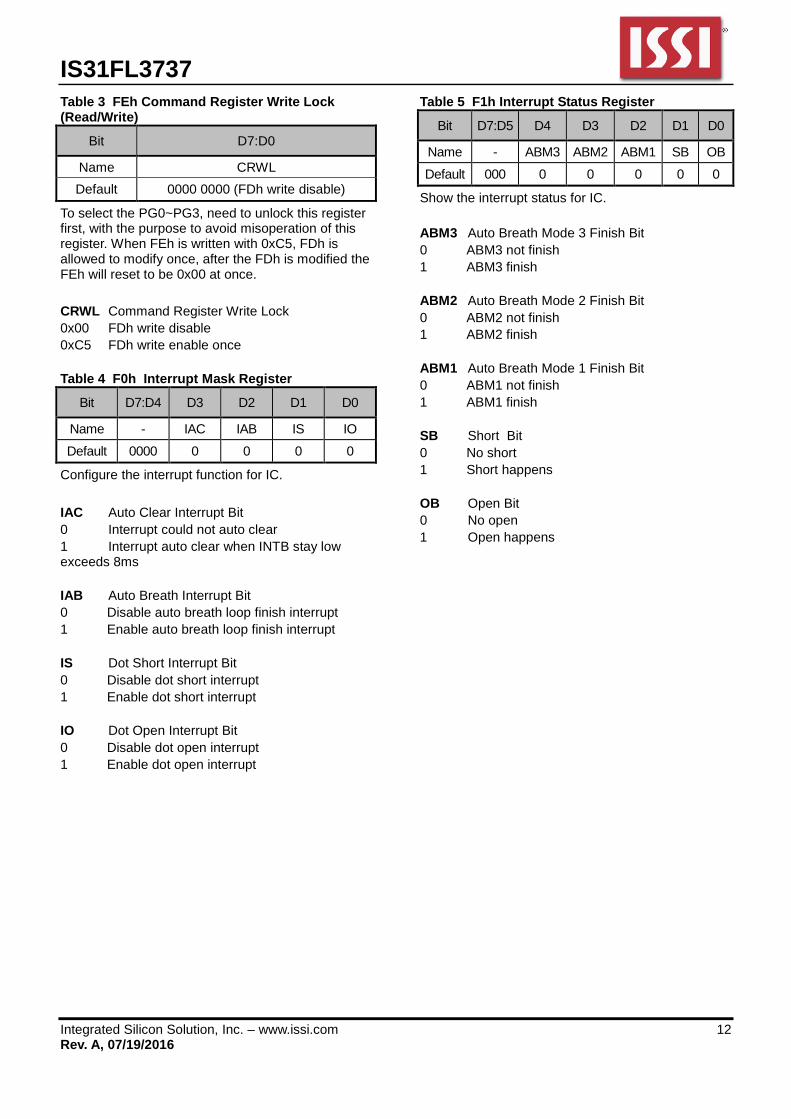
Table 3 FEh Command Register Write Lock (Read/Write)
Bit D7:D0
Name CRWL
Default 0000 0000 (FDh write disable)
To select the PG0~PG3, need to unlock this register first, with the purpose to avoid misoperation of this register. When FEh is written with 0xC5, FDh is allowed to modify once, after the FDh is modified the FEh will reset to be 0x00 at once.
CRWL Command Register Write Lock
0x00 FDh write disable
0xC5 FDh write enable once
Table 4 F0h Interrupt Mask Register
Bit D7:D4 D3 D2 D1 D0
Name - IAC IAB IS IO
Default 0000 0 0 0 0
Configure the interrupt function for IC.
IAC Auto Clear Interrupt Bit
0 Interrupt could not auto clear
1 Interrupt auto clear when INTB stay low exceeds 8ms
IAB Auto Breath Interrupt Bit
0 Disable auto breath loop finish interrupt
1 Enable auto breath loop finish interrupt
IS Dot Short Interrupt Bit
0 Disable dot short interrupt
1 Enable dot short interrupt
IO Dot Open Interrupt Bit
0 Disable dot open interrupt
1 Enable dot open interrupt
Table 5 F1h Interrupt Status Register
Bit D7:D5 D4 D3 D2 D1 D0
Name - ABM3 ABM2 ABM1 SB OB
Default 000 0 0 0 0 0
Show the interrupt status for IC.
ABM3 Auto Breath Mode 3 Finish Bit
0 ABM3 not finish
1 ABM3 finish
ABM2 Auto Breath Mode 2 Finish Bit
0 ABM2 not finish
1 ABM2 finish
ABM1 Auto Breath Mode 1 Finish Bit
0 ABM1 not finish
1 ABM1 finish
SB Short Bit
0 No short
1 Short happens
OB Open Bit
0 No open
1 Open happens
IS31FL3737
Integrated Silicon Solution, Inc. – www.issi.com 13 Rev. A, 07/19/2016
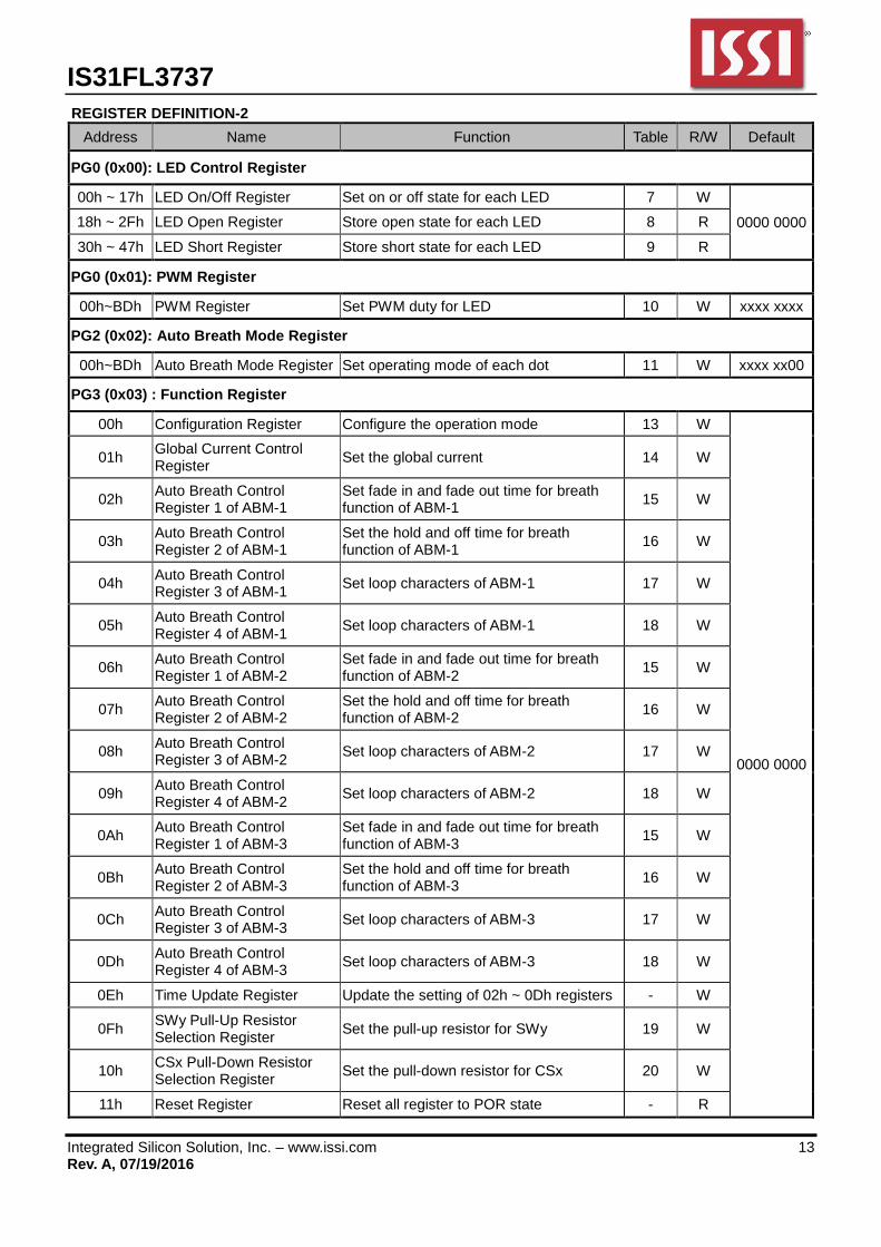
REGISTER DEFINITION-2
Address Name Function Table R/W Default
PG0 (0x00): LED Control Register
00h ~ 17h LED On/Off Register Set on or off state for each LED 7 W
0000 0000 18h ~ 2Fh LED Open Register Store open state for each LED 8 R
30h ~ 47h LED Short Register Store short state for each LED 9 R
PG0 (0x01): PWM Register
00h~BDh PWM Register Set PWM duty for LED 10 W xxxx xxxx
PG2 (0x02): Auto Breath Mode Register
00h~BDh Auto Breath Mode Register Set operating mode of each dot 11 W xxxx xx00
PG3 (0x03) : Function Register
00h Configuration Register Configure the operation mode 13 W
0000 0000
01h Global Current Control Register
Set the global current 14 W
02h Auto Breath Control Register 1 of ABM-1
Set fade in and fade out time for breath function of ABM-1
15 W
03h Auto Breath Control Register 2 of ABM-1
Set the hold and off time for breath function of ABM-1
16 W
04h Auto Breath Control Register 3 of ABM-1
Set loop characters of ABM-1 17 W
05h Auto Breath Control Register 4 of ABM-1
Set loop characters of ABM-1 18 W
06h Auto Breath Control Register 1 of ABM-2
Set fade in and fade out time for breath function of ABM-2
15 W
07h Auto Breath Control Register 2 of ABM-2
Set the hold and off time for breath function of ABM-2
16 W
08h Auto Breath Control Register 3 of ABM-2
Set loop characters of ABM-2 17 W
09h Auto Breath Control Register 4 of ABM-2
Set loop characters of ABM-2 18 W
0Ah Auto Breath Control Register 1 of ABM-3
Set fade in and fade out time for breath function of ABM-3
15 W
0Bh Auto Breath Control Register 2 of ABM-3
Set the hold and off time for breath function of ABM-3
16 W
0Ch Auto Breath Control Register 3 of ABM-3
Set loop characters of ABM-3 17 W
0Dh Auto Breath Control Register 4 of ABM-3
Set loop characters of ABM-3 18 W
0Eh Time Update Register Update the setting of 02h ~ 0Dh registers - W
0Fh SWy Pull-Up Resistor Selection Register
Set the pull-up resistor for SWy 19 W
10h CSx Pull-Down Resistor Selection Register
Set the pull-down resistor for CSx 20 W
11h Reset Register Reset all register to POR state - R
IS31FL3737
Integrated Silicon Solution, Inc. – www.issi.com 14 Rev. A, 07/19/2016
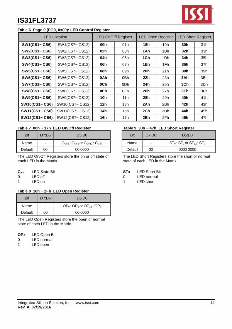
Table 6 Page 0 (PG0, 0x00): LED Control Register
LED Location LED On/Off Register LED Open Register LED Short Register
SW1(CS1~ CS6) SW1(CS7~ CS12) 00h 01h 18h 19h 30h 31h
SW2(CS1~ CS6) SW2(CS7~ CS12) 02h 03h 1Ah 1Bh 32h 33h
SW3(CS1~ CS6) SW3(CS7~ CS12) 04h 05h 1Ch 1Dh 34h 35h
SW4(CS1~ CS6) SW4(CS7~ CS12) 06h 07h 1Eh 1Fh 36h 37h
SW5(CS1~ CS6) SW5(CS7~ CS12) 08h 09h 20h 21h 38h 39h
SW6(CS1~ CS6) SW6(CS7~ CS12) 0Ah 0Bh 22h 23h 3Ah 3Bh
SW7(CS1~ CS6) SW7(CS7~ CS12) 0Ch 0Dh 24h 25h 3Ch 3Dh
SW8(CS1~ CS6) SW8(CS7~ CS12) 0Eh 0Fh 26h 27h 3Eh 3Fh
SW9(CS1~ CS6) SW9(CS7~ CS12) 10h 11h 28h 29h 40h 41h
SW10(CS1~ CS6) SW10(CS7~ CS12) 12h 13h 2Ah 2Bh 42h 43h
SW11(CS1~ CS6) SW11(CS7~ CS12) 14h 15h 2Ch 2Dh 44h 45h
SW12(CS1~ CS6) SW12(CS7~ CS12) 16h 17h 2Eh 2Fh 46h 47h
Table 7 00h ~ 17h LED On/Off Register
Bit D7:D6 D5:D0
Name - CCS6 : CCS1 or CCS12 : CCS7
Default 00 00 0000
The LED On/Off Registers store the on or off state of each LED in the Matrix.
CX-Y LED State Bit
0 LED off
1 LED on
Table 8 18h ~ 2Fh LED Open Register
Bit D7:D6 D5:D0
Name - OP6 : OP1 or OP12 : OP7
Default 00 00 0000
The LED Open Registers store the open or normal state of each LED in the Matrix.
OPx LED Open Bit
0 LED normal
1 LED open
Table 9 30h ~ 47h LED Short Register
Bit D7:D6 D5:D0
Name - ST6 : ST1 or ST12 : ST7
Default 00 0000 0000
The LED Short Registers store the short or normal state of each LED in the Matrix.
STx LED Short Bit
0 LED normal
1 LED short
IS31FL3737
Integrated Silicon Solution, Inc. – www.issi.com 15 Rev. A, 07/19/2016
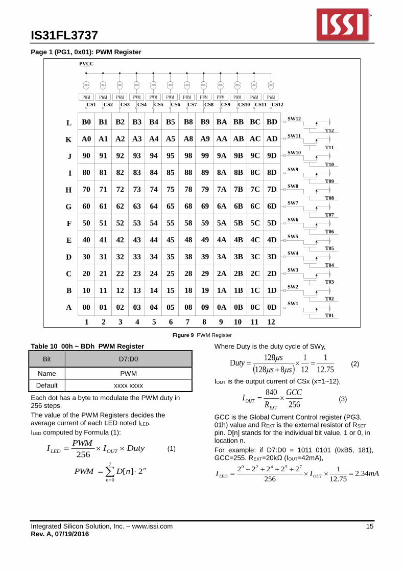
Page 1 (PG1, 0x01): PWM Register
CS1 CS2 CS3 CS4 CS5 CS6 CS7 CS8 CS9 CS10 CS11 CS12
SW12
SW2
SW9
SW10
SW4
SW5
SW11
SW6
SW7
SW3
SW8
SW1
1 2 3 4 5 6 7 8 9 10 11 12
L
B
I
J
D
E
K
F
G
C
H
A
T12
T02
T09
T10
T04
T05
T11
T06
T07
T03
T08
T01
PVCC
PWM PWMPWM PWM PWMPWM PWM PWMPWMPWM PWM PWM
00 01 02 03 04 05 08 09 0A 0B 0C 0D
B0 B1 B2 B3 B4 B5 B8 B9 BA BB BC BD
10 11 12 13 14 15 18 19 1A 1B 1C 1D
70 71 72 73 74 75 78 79 7A 7B 7C 7D
50 51 52 53 54 55 58 59 5A 5B 5C 5D
60 61 62 63 64 65 68 69 6A 6B 6C 6D
80 81 82 83 84 85 88 89 8A 8B 8C 8D
30 31 32 33 34 35 38 39 3A 3B 3C 3D
40 41 42 43 44 45 48 49 4A 4B 4C 4D
90 91 92 93 94 95 98 99 9A 9B 9C 9D
21 22 23 24 25 28 29 2A 2B 2C 2D
A0 A1 A2 A3 A4 A5 A8 A9 AA AB AC AD
20
Figure 9 PWM Register
Table 10 00h ~ BDh PWM Register
Bit D7:D0
Name PWM
Default xxxx xxxx
Each dot has a byte to modulate the PWM duty in 256 steps.
The value of the PWM Registers decides the average current of each LED noted ILED.
ILED computed by Formula (1):
DutyIPWM
I OUTLED 256
(1)
7
0
2][n
nnDPWM
Where Duty is the duty cycle of SWy,
75.12
1
12
1
8128
128D
ss
suty
(2)
IOUT is the output current of CSx (x=1~12),
256
840 GCC
RI
EXT
OUT
(3)
GCC is the Global Current Control register (PG3, 01h) value and REXT is the external resistor of RSET pin. D[n] stands for the individual bit value, 1 or 0, in location n.
For example: if D7:D0 = 1011 0101 (0xB5, 181), GCC=255. REXT=20kΩ (IOUT=42mA),
mAII OUTLED 34.275.12
1
256
22222 75420
IS31FL3737
Integrated Silicon Solution, Inc. – www.issi.com 16 Rev. A, 07/19/2016
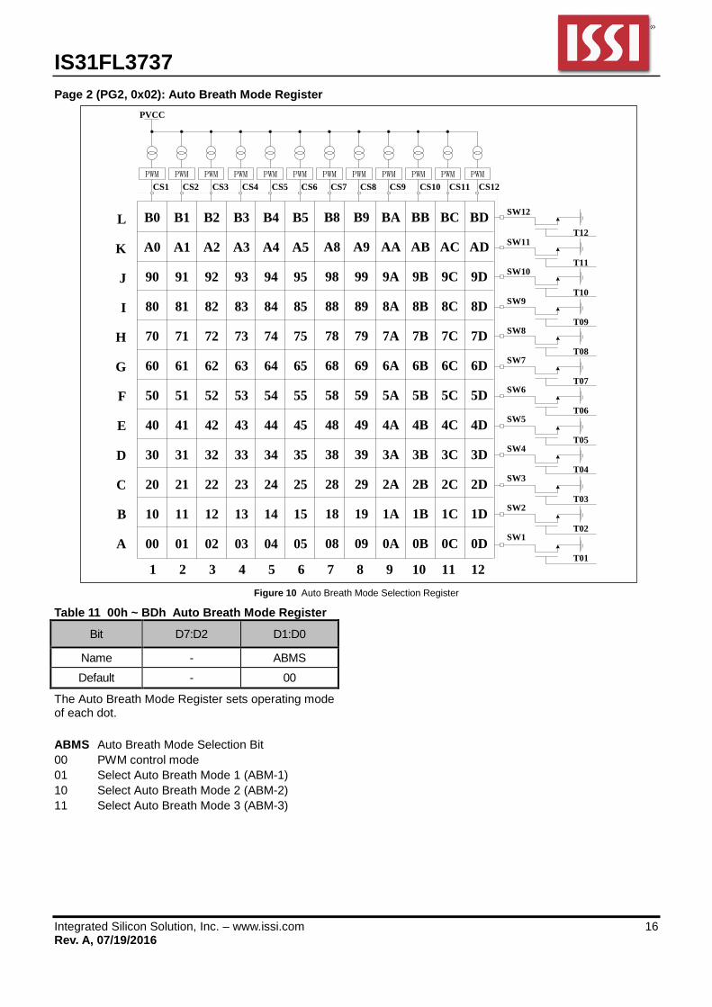
Page 2 (PG2, 0x02): Auto Breath Mode Register
CS1 CS2 CS3 CS4 CS5 CS6 CS7 CS8 CS9 CS10 CS11 CS12
SW12
SW2
SW9
SW10
SW4
SW5
SW11
SW6
SW7
SW3
SW8
SW1
1 2 3 4 5 6 7 8 9 10 11 12
L
B
I
J
D
E
K
F
G
C
H
A
T12
T02
T09
T10
T04
T05
T11
T06
T07
T03
T08
T01
PVCC
PWM PWMPWM PWM PWMPWM PWM PWMPWMPWM PWM PWM
00 01 02 03 04 05 08 09 0A 0B 0C 0D
B0 B1 B2 B3 B4 B5 B8 B9 BA BB BC BD
10 11 12 13 14 15 18 19 1A 1B 1C 1D
70 71 72 73 74 75 78 79 7A 7B 7C 7D
50 51 52 53 54 55 58 59 5A 5B 5C 5D
60 61 62 63 64 65 68 69 6A 6B 6C 6D
80 81 82 83 84 85 88 89 8A 8B 8C 8D
30 31 32 33 34 35 38 39 3A 3B 3C 3D
40 41 42 43 44 45 48 49 4A 4B 4C 4D
90 91 92 93 94 95 98 99 9A 9B 9C 9D
21 22 23 24 25 28 29 2A 2B 2C 2D
A0 A1 A2 A3 A4 A5 A8 A9 AA AB AC AD
20
Figure 10 Auto Breath Mode Selection Register
Table 11 00h ~ BDh Auto Breath Mode Register
Bit D7:D2 D1:D0
Name - ABMS
Default - 00
The Auto Breath Mode Register sets operating mode of each dot.
ABMS Auto Breath Mode Selection Bit
00 PWM control mode
01 Select Auto Breath Mode 1 (ABM-1)
10 Select Auto Breath Mode 2 (ABM-2)
11 Select Auto Breath Mode 3 (ABM-3)
IS31FL3737
Integrated Silicon Solution, Inc. – www.issi.com 17 Rev. A, 07/19/2016
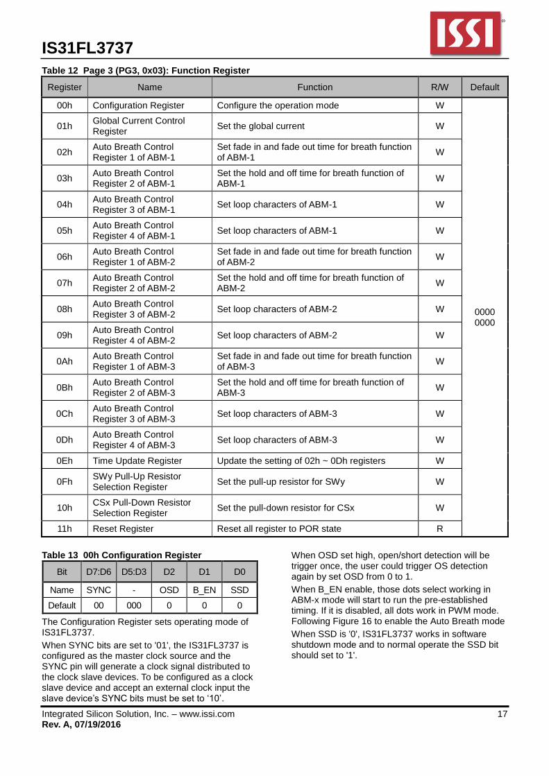
Table 12 Page 3 (PG3, 0x03): Function Register
Register Name Function R/W Default
00h Configuration Register Configure the operation mode W
0000 0000
01h Global Current Control Register
Set the global current W
02h Auto Breath Control Register 1 of ABM-1
Set fade in and fade out time for breath function of ABM-1
W
03h Auto Breath Control Register 2 of ABM-1
Set the hold and off time for breath function of ABM-1
W
04h Auto Breath Control Register 3 of ABM-1
Set loop characters of ABM-1 W
05h Auto Breath Control Register 4 of ABM-1
Set loop characters of ABM-1 W
06h Auto Breath Control Register 1 of ABM-2
Set fade in and fade out time for breath function of ABM-2
W
07h Auto Breath Control Register 2 of ABM-2
Set the hold and off time for breath function of ABM-2
W
08h Auto Breath Control Register 3 of ABM-2
Set loop characters of ABM-2 W
09h Auto Breath Control Register 4 of ABM-2
Set loop characters of ABM-2 W
0Ah Auto Breath Control Register 1 of ABM-3
Set fade in and fade out time for breath function of ABM-3
W
0Bh Auto Breath Control Register 2 of ABM-3
Set the hold and off time for breath function of ABM-3
W
0Ch Auto Breath Control Register 3 of ABM-3
Set loop characters of ABM-3 W
0Dh Auto Breath Control Register 4 of ABM-3
Set loop characters of ABM-3 W
0Eh Time Update Register Update the setting of 02h ~ 0Dh registers W
0Fh SWy Pull-Up Resistor Selection Register
Set the pull-up resistor for SWy W
10h CSx Pull-Down Resistor Selection Register
Set the pull-down resistor for CSx W
11h Reset Register Reset all register to POR state R
Table 13 00h Configuration Register
Bit D7:D6 D5:D3 D2 D1 D0
Name SYNC - OSD B_EN SSD
Default 00 000 0 0 0
The Configuration Register sets operating mode of IS31FL3737.
When SYNC bits are set to '01', the IS31FL3737 is configured as the master clock source and the SYNC pin will generate a clock signal distributed to the clock slave devices. To be configured as a clock slave device and accept an external clock input the slave device’s SYNC bits must be set to ‘10’.
When OSD set high, open/short detection will be trigger once, the user could trigger OS detection again by set OSD from 0 to 1.
When B_EN enable, those dots select working in ABM-x mode will start to run the pre-established timing. If it is disabled, all dots work in PWM mode. Following Figure 16 to enable the Auto Breath mode
When SSD is '0', IS31FL3737 works in software shutdown mode and to normal operate the SSD bit should set to '1'.
IS31FL3737
Integrated Silicon Solution, Inc. – www.issi.com 18 Rev. A, 07/19/2016
SYNC Synchronize Configuration
00/11 High Impedance
01 Master
10 Slave
OSD Open/Short Detection Enable Bit
0 Disable open/short detection
1 Enable open/short detection
B_EN Auto Breath Enable
0 PWM Mode Enable
1 Auto Breath Mode Enable
SSD Software Shutdown Control
0 Software shutdown
1 Normal operation
Table 14 01h Global Current Control Register
Bit D7:D0
Name GCCx
Default 0000 0000
The Global Current Control Register modulates all CSx (x=1~12) DC current which is noted as IOUT in 256 steps.
IOUT is computed by the Formula (3):
256
840 GCC
RI
EXT
OUT (3)
7
0
2][n
nnDGCC
Where D[n] stands for the individual bit value, 1 or 0, in location n, REXT is the external resistor of RSET pin.
For example: if D7:D0 = 1011 0101,
EXT
OUTR
I840
256
22222 75420
Table 15 02h, 06h, 0Ah Auto Breath Control Register 1 of ABM-x
Bit D7:D5 D4:D1 D0
Name T1 T2 -
Default 000 0000 0
Auto Breath Control Register 1 set the T1&T2 time in Auto Breath Mode.
T1 T1 Setting
000 0.21s
001 0.42s
010 0.84s
011 1.68s
100 3.36s
101 6.72s
110 13.44s
111 26.88s
T2 T2 Setting
0000 0s
0001 0.21s
0010 0.42s
0011 0.84s
0100 1.68s
0101 3.36s
0110 6.72s
0111 13.44s
1000 26.88s
Others Unavailable
Table 16 03h, 07h, 0Bh Auto Breath Control Register 2 of ABM-x
Bit D7:D5 D4:D1 D0
Name T3 T4 -
Default 000 0000 0
Auto Breath Control Register 2 set the T3&T4 time in Auto Breath Mode.
T3 T3 Setting
000 0.21s
001 0.42s
010 0.84s
011 1.68s
100 3.36s
101 6.72s
110 13.44s
111 26.88s
T4 T4 Setting
0000 0s
0001 0.21s
0010 0.42s
0011 0.84s
0100 1.68s
0101 3.36s
0110 6.72s
0111 13.44s
1000 26.88s
1001 53.76s
1010 107.52s
Others Unavailable
IS31FL3737
Integrated Silicon Solution, Inc. – www.issi.com 19 Rev. A, 07/19/2016
Table 17 04h, 08h, 0Ch Auto Breath Control Register 3 of ABM-x
Bit D7:D6 D5:D4 D3:D0
Name LE LB LTA
Default 00 00 0000
Total loop times= LTA ×256 + LTB.
For example, if LTA=2, LTB=100, the total loop times is 256×2+100= 612 times.
For the counting of breathing times, do follow Figure 16 to enable the Auto Breath Mode.
If the loop start from T4,
T4->T1->T2->T3(1)->T4->T1->T2->T3(2)->T4->T1->... and so on.
If the loop not start from T4,
Tx->T3(1) ->T4->T1->T2->T3(2)->T4-> T1->... and so on.
If the loop ends at off state (End of T3), the LED will be off state at last. If the loop ends at on state (End of T1), the LED will run an extra T4&T1, which are not included in loop.
LB Loop Beginning Time
00 Loop begin from T1
01 Loop begin from T2
10 Loop begin from T3
11 Loop begin from T4
LE Loop End Time
00 Loop end at off state (End of T3)
01 Loop end at on state (End of T1)
LTA 8-11 Bits Of Loop Times
0000 Endless loop
0001 1
0010 2
… …
1111 15
T1 T2 T3 T4 T1
1 Loop
Figure 11 Auto Breathing Function
Table 18 05h, 09h, 0Dh Auto Breath Control Register 4 of ABM-x
Bit D7:D0
Name LTB
Default 0000 0000
Total loop times= LTA ×256 + LTB.
For example, if LTA=2, LTB=100, the total loop times is 256×2+100= 612 times.
LTB 0-7 Bits Of Loop Times
0000 0000 Endless loop
0000 0001 1
0000 0010 2
… …
1111 1111 255
0Eh Time Update Register (02h~0Dh) The data sent to the time registers (02h~0Dh) will be stored in temporary registers. A write operation of “0000 0000” data to the Time Update Register is required to update the registers (02h~0Dh). Please follow Figure 16 to enable the Auto Breath mode and update the time parameters.
Table 19 0Fh SWy Pull-Up Resistor Selection Register
Bit D7:D3 D2:D0
Name - PUR
Default 00000 000
Set pull-up resistor for SWy.
PUR SWy Pull-up Resistor Selection Bit
000 No pull-up resistor
001 0.5kΩ
010 1.0kΩ
011 2.0kΩ
100 4.0kΩ
101 8.0kΩ
110 16kΩ
111 32kΩ
Table 20 10h CSx Pull-Down Resistor Selection Register
Bit D7:D3 D2:D0
Name - PDR
Default 00000 000
Set the pull-down resistor for CSx.
IS31FL3737
Integrated Silicon Solution, Inc. – www.issi.com 20 Rev. A, 07/19/2016
PDR CSx Pull-down Resistor Selection Bit
000 No pull-down resistor
001 0.5kΩ
010 1.0kΩ
011 2.0kΩ
100 4.0kΩ
101 8.0kΩ
110 16kΩ
111 32kΩ
11h Reset Register
Once user read the Reset Register, IS31FL3737 will reset all the IS31FL3737 registers to their default value. On initial power-up, the IS31FL3737 registers are reset to their default values for a blank display.
IS31FL3737
Integrated Silicon Solution, Inc. – www.issi.com 21 Rev. A, 07/19/2016
APPLICATION INFORMATION
SW1
SW2
SW12
tNOL=8µs
SW3
SW4
SW5
SW7
SW11
SW6
SW8
SW9
SW10
CS1
CS12
tSCAN=128µs
Scanning cycle T=1.632ms((128+8)×12)
PWM Duty is variable from 0/256~255/256
00h 00h10h 20h 30h 40h 50h 60h 70h 80h 90h A0h B0h
0Dh 0Dh1Dh 2Dh 3Dh 4Dh 5Dh 6Dh 7Dh 8Dh 9Dh ADh BDh
IOUT=840/REXT×GCC/256
(GCC=0~255)
De-Ghost time
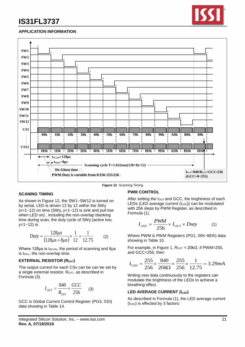
Figure 12 Scanning Timing
SCANING TIMING
As shown in Figure 12, the SW1~SW12 is turned on by serial, LED is driven 12 by 12 within the SWy (x=1~12) on time (SWy, y=1~12) is sink and pull low when LED on) , including the non-overlap blanking time during scan, the duty cycle of SWy (active low, y=1~12) is:
75.12
1
12
1
8128
128D
ss
suty
(2)
Where 128μs is tSCAN, the period of scanning and 8μs is tNOL, the non-overlap time.
EXTERNAL RESISTOR (REXT)
The output current for each CSx can be can be set by a single external resistor, REXT, as described in Formula (3).
256
840 GCC
RI
EXT
OUT (3)
GCC is Global Current Control Register (PG3, 01h) data showing in Table 14.
PWM CONTROL
After setting the IOUT and GCC, the brightness of each LEDs (LED average current (ILED)) can be modulated with 256 steps by PWM Register, as described in Formula (1).
DutyIPWM
I OUTLED 256
(1)
Where PWM is PWM Registers (PG1, 00h~BDh) data showing in Table 10.
For example, in Figure 1, REXT = 20kΩ, if PWM=255, and GCC=255, then
mAk
29.375.12
1
256
255
20
840
256
255ILED
Writing new data continuously to the registers can modulate the brightness of the LEDs to achieve a breathing effect.
LED AVERAGE CURRENT (ILED)
As described in Formula (1), the LED average current (ILED) is effected by 3 factors:
IS31FL3737
Integrated Silicon Solution, Inc. – www.issi.com 22 Rev. A, 07/19/2016
1. REXT, resistor which is connected RSET pin and GND. REXT sets the current of all CSx(x=1~12) based on Formula (3).
2. Global Current Control Register (PG3, 01h). This register adjusts all CSx (x=1~12) output currents by 256 steps as shown in Formula (3).
3. PWM Registers (PG1, 00h~BFh), every LED has an own PWM register. PWM Registers adjust individual LED average current by 256 steps as shown in Formula (1).
GAMMA CORRECTION
In order to perform a better visual LED breathing effect we recommend using a gamma corrected PWM value to set the LED intensity. This results in a reduced number of steps for the LED intensity setting, but causes the change in intensity to appear more linear to the human eye.
Gamma correction, also known as gamma compression or encoding, is used to encode linear luminance to match the non-linear characteristics of display. Since the IS31FL3737 can modulate the brightness of the LEDs with 256 steps, a gamma correction function can be applied when computing each subsequent LED intensity setting such that the changes in brightness matches the human eye's brightness curve.
Table 21 32 Gamma Steps with 256 PWM Steps
C(0) C(1) C(2) C(3) C(4) C(5) C(6) C(7)
0 1 2 4 6 10 13 18
C(8) C(9) C(10) C(11) C(12) C(13) C(14) C(15)
22 28 33 39 46 53 61 69
C(16) C(17) C(18) C(19) C(20) C(21) C(22) C(23)
78 86 96 106 116 126 138 149
C(24) C(25) C(26) C(27) C(28) C(29) C(30) C(31)
161 173 186 199 212 226 240 255
0
32
64
96
128
160
192
224
256
0 4 8 12 16 20 24 28 32
PW
M D
ata
Intensity Steps
Figure 13 Gamma Correction (32 Steps)
Choosing more gamma steps provides for a more continuous looking breathing effect. This is useful for very long breathing cycles. The recommended
configuration is defined by the breath cycle T. When T=1s, choose 32 gamma steps, when T=2s, choose 64 gamma steps. The user must decide the final number of gamma steps not only by the LED itself, but also based on the visual performance of the finished product.
Table 22 64 Gamma Steps with 256 PWM Steps
C(0) C(1) C(2) C(3) C(4) C(5) C(6) C(7)
0 1 2 3 4 5 6 7
C(8) C(9) C(10) C(11) C(12) C(13) C(14) C(15)
8 10 12 14 16 18 20 22
C(16) C(17) C(18) C(19) C(20) C(21) C(22) C(23)
24 26 29 32 35 38 41 44
C(24) C(25) C(26) C(27) C(28) C(29) C(30) C(31)
47 50 53 57 61 65 69 73
C(32) C(33) C(34) C(35) C(36) C(37) C(38) C(39)
77 81 85 89 94 99 104 109
C(40) C(41) C(42) C(43) C(44) C(45) C(46) C(47)
114 119 124 129 134 140 146 152
C(48) C(49) C(50) C(51) C(52) C(53) C(54) C(55)
158 164 170 176 182 188 195 202
C(56) C(57) C(58) C(59) C(60) C(61) C(62) C(63)
209 216 223 230 237 244 251 255
0
32
64
96
128
160
192
224
256
0 8 16 24 32 40 48 56 64
PW
M D
ata
Intensity Steps
Figure 14 Gamma Correction (64 Steps)
Note: The data of 32 gamma steps is the standard value and the data of 64 gamma steps is the recommended value.
OPERATING MODE Each dot of IS31FL3737 has two selectable operating modes, PWM Mode and Auto Breath Mode.
PWM Mode By setting the Auto Breath Mode Register bits of the Page 2 (PG2, 00h~BFh) to “00”, or disable the B_EN bit of Configure Register (PG3, 00h), the IS31FL3737 operates in PWM Mode. The brightness of each LED can be modulated with 256 steps by PWM registers. For example, if the data in PWM Register is “0000 0100”, then the PWM is the fourth step.
IS31FL3737
Integrated Silicon Solution, Inc. – www.issi.com 23 Rev. A, 07/19/2016
Writing new data continuously to the registers can modulate the brightness of the LEDs to achieve a breathing effect.
Auto Breath Mode
By setting the B_EN bit of the Configuration Register (PG3, 00h) to “1”, breath function enables. When set the B_EN bit to “0”, breath function disables.
By setting the Auto Breath Mode Register bits of the Page 2 (PG2, 00h~BFh) to “01” (ABM-1), “10” (ABM-2) or “11” (ABM-3), the IS31FL3737 operates in Auto Breath Mode.
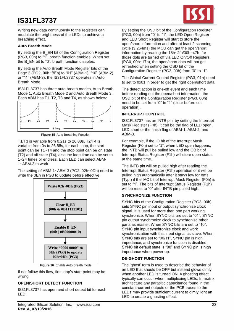
IS31FL3737 has three auto breath modes, Auto Breath Mode 1, Auto Breath Mode 2 and Auto Breath Mode 3. Each ABM has T1, T2, T3 and T4, as shown below:
T1 T2 T3 T4 T1
1 Loop
Figure 15 Auto Breathing Function
T1/T3 is variable from 0.21s to 26.88s, T2/T4 is variable from 0s to 26.88s, for each loop, the start point can be T1~T4 and the stop point can be on state (T2) and off state (T4), also the loop time can be set to 1~212 times or endless. Each LED can select ABM-1~ABM-3 to work.
The setting of ABM-1~ABM-3 (PG2, 02h~0Dh) need to write the 0Eh in PG3 to update before effective.
Write 02h~0Dh (PG3)
Clear B_EN
(00h & 0B11111101)
Enable B_EN
(00h | 0B00000010)
Write “0000 0000” to
0Eh (PG3) to update
02h~0Dh (PG3)
Figure 16 Enable Auto Breath mode
If not follow this flow, first loop’s start point may be wrong
OPEN/SHORT DETECT FUNCTION
IS31FL3737 has open and short detect bit for each LED.
By setting the OSD bit of the Configuration Register (PG3, 00h) from "0" to “1”, the LED Open Register and LED Short Register will start to store the open/short information and after at least 2 scanning cycle (3.264ms) the MCU can get the open/short information by reading the 18h~2fh/30h~47h, for those dots are turned off via LED On/Off Registers (PG0, 00h~17h), the open/short data will not get refreshed when setting the OSD bit of the Configuration Register (PG3, 00h) from "0" to “1”.
The Global Current Control Register (PG3, 01h) need to set to 0x01 in order to get the right open/short data.
The detect action is one-off event and each time before reading out the open/short information, the OSD bit of the Configuration Register (PG3, 00h) need to be set from "0" to “1” (clear before set operation).
INTERRUPT CONTROL
IS31FL3737 has an INTB pin, by setting the Interrupt Mask Register (F0h), it can be the flag of LED open, LED short or the finish flag of ABM-1, ABM-2, and ABM-3.
For example, if the IO bit of the Interrupt Mask Register (F0h) set to “1”, when LED open happens, the INTB will pull be pulled low and the OB bit of Interrupt Status Register (F1h) will store open status at the same time.
The INTB pin will be pulled high after reading the Interrupt Status Register (F1h) operation or it will be pulled high automatically after it stays low for 8ms (Typ.) if the IAC bit of Interrupt Mask Register (F0h) is set to “1”. The bits of Interrupt Status Register (F1h) will be reset to “0” after INTB pin pulled high.
SYNCHRONIZE FUNCTION
SYNC bits of the Configuration Register (PG3, 00h) sets SYNC pin input or output synchronize clock signal. It is used for more than one part working synchronize. When SYNC bits are set to “01”, SYNC pin output synchronize clock to synchronize other parts as master. When SYNC bits are set to “10”, SYNC pin input synchronize clock and work synchronization with this input signal as slave. When SYNC bits are set to “00/11”, SYNC pin is high impedance, and synchronize function is disabled. SYNC bit default state is “00” and SYNC pin is high impedance when power up.
DE-GHOST FUNCTION
The ‘ghost’ term is used to describe the behavior of an LED that should be OFF but instead glows dimly when another LED is turned ON. A ghosting effect typically can occur when multiplexing LEDs. In matrix architecture any parasitic capacitance found in the constant-current outputs or the PCB traces to the LEDs may provide sufficient current to dimly light an LED to create a ghosting effect.
IS31FL3737
Integrated Silicon Solution, Inc. – www.issi.com 24 Rev. A, 07/19/2016
To prevent this LED ghost effect, the IS31FL3737 has integrated pull-up resistors for each SWy (y=1~12) and pull-down resistors for each CSx (x=1~12). Select the right SWy pull-up resistor (PG3, 0Fh) and CSx pull-down resistor (PG3, 10h) which eliminates the ghost LED for a particular matrix layout configuration.
Typically, selecting the 32kΩ will be sufficient to eliminate the LED ghost phenomenon.
The SWy pull-up resistors and CSx pull-down resistors are active only when the CSx/SWy outputs are in the OFF state and therefore no power is lost through these resistors
IIC RESET
The IIC will be reset if the IICRST pin is pull-high, when normal operating the IIC bus, the IICRST pin need to keep low.
SHUTDOWN MODE
Shutdown mode can be used as a means of reducing power consumption. During shutdown mode all registers retain their data.
Software Shutdown
By setting SSD bit of the Configuration Register (PG3, 00h) to “0”, the IS31FL3737 will operate in software shutdown mode. When the IS31FL3737 is in software shutdown, all current sources are switched off, so that the matrix is blanked. All registers can be operated. Typical current consume is 3μA.
Hardware Shutdown
The chip enters hardware shutdown when the SDB pin is pulled low. All analog circuits are disabled during hardware shutdown, typical the current consume is 3μA.
The chip releases hardware shutdown when the SDB pin is pulled high. During hardware shutdown state Function Register can be operated.
If VCC has risk drop below 1.75V but above 0.1V during SDB pulled low, please re-initialize all Function Registers before SDB pulled high.
POWER DISSIPATION
The power dissipation of the IS31FL3737 can calculate as below:
P3737=IPVCC×PVCC+ IQ×DVCC(AVCC) - IPVCC×VF(AVR) (4)
≈IPVCC×PVCC - IPVCC×VF(AVR)
≈IPVCC×(PVCC - VF(AVR))
Where IPVCC is the current of PVCC and VF(AVR) is the average forward of all the LED.
For example, if REXT=20kΩ, GCC=255, PWM=255, PVCC=5V, VF(AVR)=3.5V@42mA, then the IPVCC=42mA×12×12/12.75=474.4mA.
P3737=474.4mA ×(5V-3.5V)=0.806W
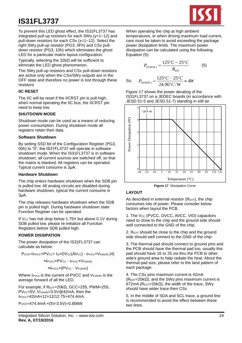
When operating the chip at high ambient temperatures, or when driving maximum load current, care must be taken to avoid exceeding the package power dissipation limits. The maximum power dissipation can be calculated using the following Equation (5):
JA
MAXDR
CCP
25125)(
(5)
So, WWC
CCP MAXD 4
/96.24
25125)(
Figure 17 shows the power derating of the IS31FL3737 on a JEDEC boards (in accordance with JESD 51-5 and JESD 51-7) standing in still air.
0
1
2
3
4
5
Temperature (°C)
Po
wer
Dis
sip
atio
n (
W)
-40 -25 -10 5 20 35 50 65 80 95 110 125
QFN-40
Figure 17 Dissipation Curve
LAYOUT
As described in external resistor (REXT), the chip consumes lots of power. Please consider below factors when layout the PCB.
1. The VCC (PVCC, DVCC, AVCC, VIO) capacitors need to close to the chip and the ground side should well connected to the GND of the chip.
2. REXT should be close to the chip and the ground side should well connect to the GND of the chip.
3. The thermal pad should connect to ground pins and the PCB should have the thermal pad too, usually this pad should have 16 or 25 via thru the PCB to other side’s ground area to help radiate the heat. About the thermal pad size, please refer to the land pattern of each package.
4. The CSx pins maximum current is 42mA (REXT=20kΩ), and the SWy pins maximum current is 672mA (REXT=20kΩ), the width of the trace, SWy should have wider trace then CSx.
5. In the middle of SDA and SCL trace, a ground line is recommended to avoid the effect between these two lines.
IS31FL3737
Integrated Silicon Solution, Inc. – www.issi.com 25 Rev. A, 07/19/2016
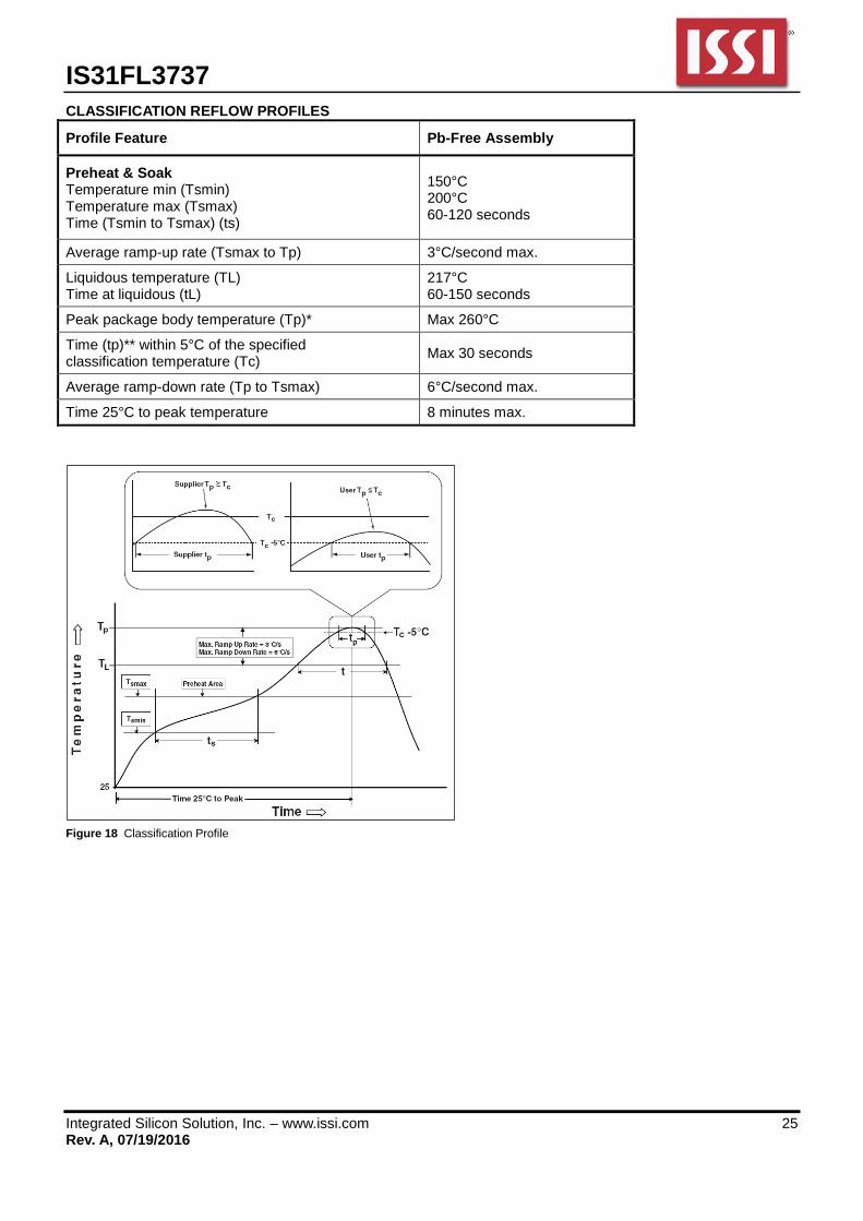
CLASSIFICATION REFLOW PROFILES
Profile Feature Pb-Free Assembly
Preheat & Soak Temperature min (Tsmin) Temperature max (Tsmax) Time (Tsmin to Tsmax) (ts)
150°C 200°C 60-120 seconds
Average ramp-up rate (Tsmax to Tp) 3°C/second max.
Liquidous temperature (TL) Time at liquidous (tL)
217°C 60-150 seconds
Peak package body temperature (Tp)* Max 260°C
Time (tp)** within 5°C of the specified classification temperature (Tc)
Max 30 seconds
Average ramp-down rate (Tp to Tsmax) 6°C/second max.
Time 25°C to peak temperature 8 minutes max.
Figure 18 Classification Profile
IS31FL3737
Integrated Silicon Solution, Inc. – www.issi.com 26 Rev. A, 07/19/2016
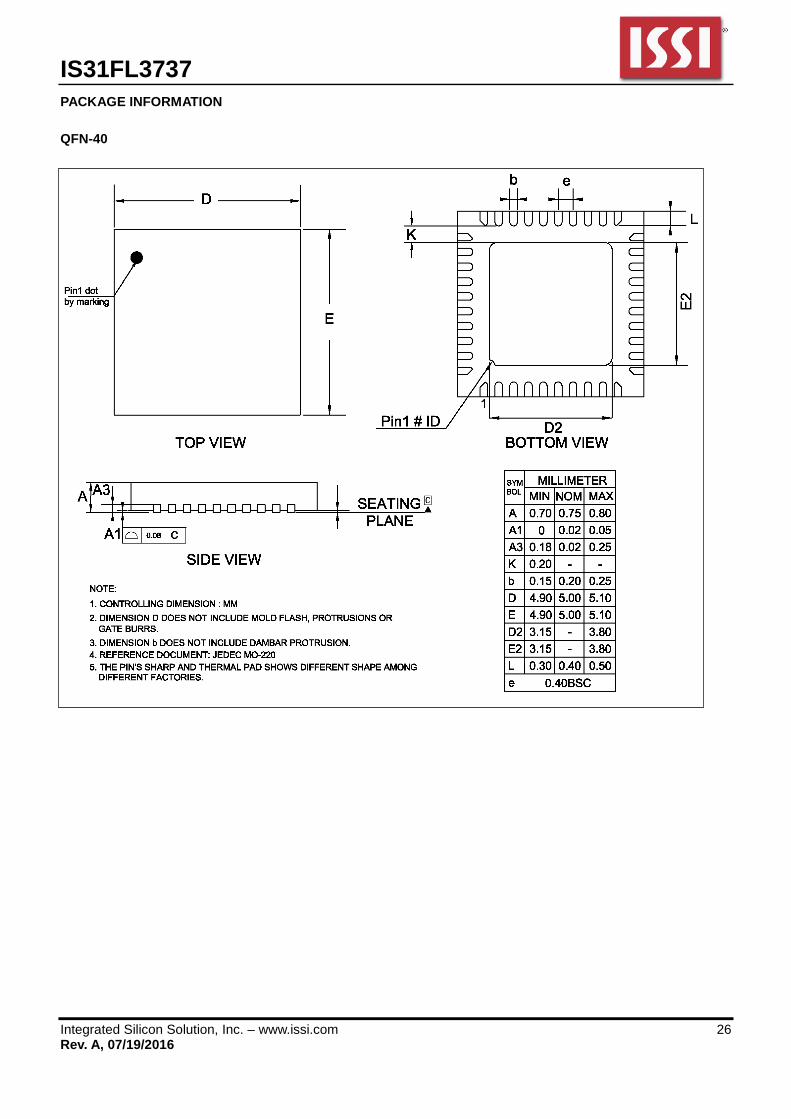
PACKAGE INFORMATION
QFN-40
IS31FL3737
Integrated Silicon Solution, Inc. – www.issi.com 27 Rev. A, 07/19/2016
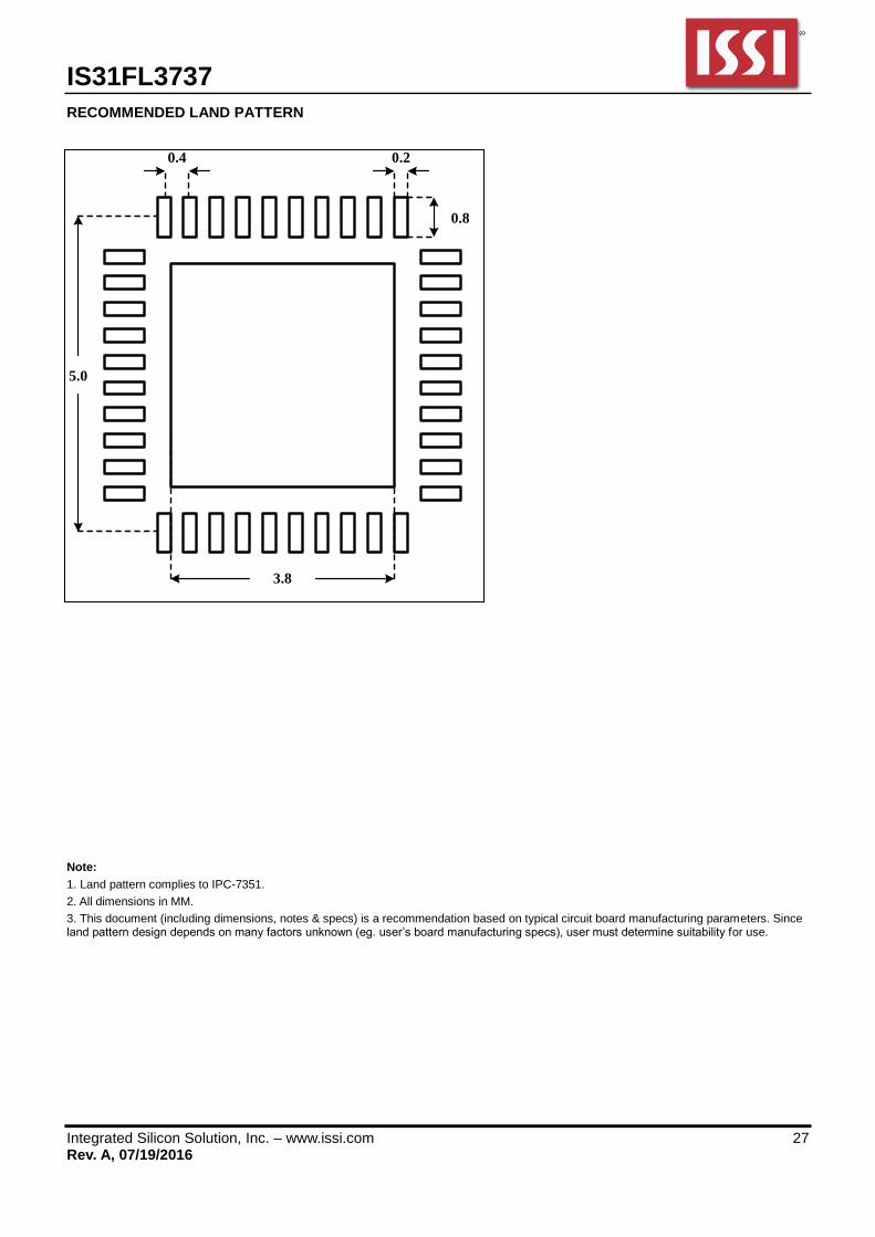
RECOMMENDED LAND PATTERN
0.4
0.8
0.2
5.0
3.8
Note:
1. Land pattern complies to IPC-7351.
2. All dimensions in MM.
3. This document (including dimensions, notes & specs) is a recommendation based on typical circuit board manufacturing parameters. Since land pattern design depends on many factors unknown (eg. user’s board manufacturing specs), user must determine suitability for use.
IS31FL3737
Integrated Silicon Solution, Inc. – www.issi.com 28 Rev. A, 07/19/2016
REVISION HISTORY
Revision Detail Information Date
0A Initial release 2016.05.09
0B 1 Update Figure 1, 2 2 Correct a spell mistake in page 1 3 update the IOUT / ILED limitation
2016.06.28
A Update I2C READING OPERATIOON section and Figure 8 2016.07.19


![Denial-of-Service Open Threat Signaling (DOTS). · architecture, called DDoS Open Threat Signaling (DOTS) [I-D.ietf-dots-architecture], in which a DOTS client can inform a DOTS server](https://static.fdocuments.net/doc/165x107/6018af73a358a566d57c4efb/denial-of-service-open-threat-signaling-dots-architecture-called-ddos-open-threat.jpg)