(12) United States Patent (10) Patent No.: US 8,346,832 B2 ...
21
US008346832B2 (12) United States Patent (10) Patent No.: US 8,346,832 B2 Mudge et a1. (45) Date of Patent: Jan. 1, 2013 (54) RANDOM NUMBER GENERATOR FOREIGN PATENT DOCUMENTS JP 2003-084970 3/2003 (75) Inventors: Trevor Nigel Mudge, Ann Arbor, MI (Continued) (US); David Theodore BlaauW, Ann Arbor, Ml (US); Carlos AlfOIlSO OTHER PUBLICATIONS Tokunaga, Ann Arbor, MI (US) C Hoggins, C D’Alessandro, D Kinniment, A Yakovlev, Securing (73) Assigneez The Regents of the University of On-Chip Operations against Timing Attacks, Sep. 2005, University Michigan’ AnnArbOr, MI (Us) ofNewcastle upon Tyne,-pp. 1-8.* I I I I I I S Walker, S Foo, Evaluating Metastability in Electronic Circuits for ( * ) Notice: Subject to any disclaimer, the term of this Random NO‘ Generanon’ IEEE’ 2001’ pp‘ 99'l01'* patent is extended or adjusted under 35 (Continued) U.S.C. 154(b) by 1430 days. Primary Examiner * Chuong D Ngo (21) APP1- NOJ 11/826,996 Assistant Examiner * Kevin G Hughes _ (74) Attorney, Agent, or Firm * Nixon & Vanderhye PC. (22) Filed: Jul. 19, 2007 (57) ABSTRACT (65) Prior Publication Data _ _ _ _ _ A circuit for generating a random output value is disclosed Us Zoos/0091755 A1 APR 17, 2008 that comprises: a bistable circuit having two stable states in which a 0 or a 1 is output and having a balanced metastable Related U-s- Application Data state in which a ?oating value between 0 and 1 is output, said (60) Provisional application NO_ 60/851,073’ ?led on Oct bistable circuit resolving from said metastable state to one of 12, 2006 said stable states on being switched on, said state depending on a voltage level at a port on said bistable circuit; a voltage (51) In‘; C]_ level control circuit for controlling a voltage level at said port G06F 1/02 (200601) on said bistable circuit; a time measuring circuit for measur G06F 7/58 (200601) ing a switching time taken for said bistable circuit to switch (52) us. Cl. ..................................................... .. 708/250 from Said metastable State to one Ofsaid Stable States follow (58) Field of Classi?cation Search ......... .. 708/25m256 mg Switch 9“; and 095m} logicl fog Controlling 581d ‘?ne - - - measuring circuit, sa1 vo tage eve contro circuit an a See apphcanon ?le for Complete Search hlstory' switching off and on of said bistable circuit, said control logic (56) References Cited being adapted to perform a following sequence: control said US. PATENT DOCUMENTS 4,752,748 A * 6/1988 5,166,959 A * 11/1992 .......... .. 331/1 A 377/20 GrZesZykowski Chu et al. .. voltage level control circuit to set a predetermined voltage level at said port on said bistable circuit, switch said bistable circuit on, detect a measured switching time, and turn said bistable circuit off and if said measured switching time is 5,826,061 A * 10/ 1998 Walp .. 716/108 longer than a predetermined value, output said resolved stable 6,771,104 B2 * 8/2004 HMS ~ 327/ 164 state of said bistable circuit as said random output value. 6,795,837 B1 * 9/2004 Wells .............................. .. 708/3 (Continued) 20 Claims, 13 Drawing Sheets Cycle to cycle bit generation Resolution time based grading ‘F ______________________________________ u '1 .. ; Metastable - and metastability control : circuit Start : I i 5 id ‘lirne to i I Charge 1 ; Digital — 1 I control array : ; stop Converter : E E 1 Random bit E l I ............................ - - I i Statistiml I E Control Analysis id I E """"""""""""""" ‘ ‘: Quali?er : Random Output ....010010l_.... + Quality
Transcript of (12) United States Patent (10) Patent No.: US 8,346,832 B2 ...

US008346832B2
(12) United States Patent (10) Patent No.: US 8,346,832 B2 Mudge et a1. (45) Date of Patent: Jan. 1, 2013
(54) RANDOM NUMBER GENERATOR FOREIGN PATENT DOCUMENTS JP 2003-084970 3/2003
(75) Inventors: Trevor Nigel Mudge, Ann Arbor, MI (Continued) (US); David Theodore BlaauW, Ann Arbor, Ml (US); Carlos AlfOIlSO OTHER PUBLICATIONS Tokunaga, Ann Arbor, MI (US)
C Hoggins, C D’Alessandro, D Kinniment, A Yakovlev, Securing (73) Assigneez The Regents of the University of On-Chip Operations against Timing Attacks, Sep. 2005, University
Michigan’ AnnArbOr, MI (Us) ofNewcastle upon Tyne,-pp. 1-8.* I I I I I I S Walker, S Foo, Evaluating Metastability in Electronic Circuits for
( * ) Notice: Subject to any disclaimer, the term of this Random NO‘ Generanon’ IEEE’ 2001’ pp‘ 99'l01'*
patent is extended or adjusted under 35 (Continued) U.S.C. 154(b) by 1430 days.
Primary Examiner * Chuong D Ngo (21) APP1- NOJ 11/826,996 Assistant Examiner * Kevin G Hughes
_ (74) Attorney, Agent, or Firm * Nixon & Vanderhye PC. (22) Filed: Jul. 19, 2007
(57) ABSTRACT (65) Prior Publication Data _ _ _ _ _
A circuit for generating a random output value is disclosed Us Zoos/0091755 A1 APR 17, 2008 that comprises: a bistable circuit having two stable states in
which a 0 or a 1 is output and having a balanced metastable Related U-s- Application Data state in which a ?oating value between 0 and 1 is output, said
(60) Provisional application NO_ 60/851,073’ ?led on Oct bistable circuit resolving from said metastable state to one of 12, 2006 said stable states on being switched on, said state depending
on a voltage level at a port on said bistable circuit; a voltage (51) In‘; C]_ level control circuit for controlling a voltage level at said port
G06F 1/02 (200601) on said bistable circuit; a time measuring circuit for measur G06F 7/58 (200601) ing a switching time taken for said bistable circuit to switch
(52) us. Cl. ..................................................... .. 708/250 from Said metastable State to one Ofsaid Stable States follow
(58) Field of Classi?cation Search ......... .. 708/25m256 mg Switch 9“; and 095m} logicl fog Controlling 581d ‘?ne - - - measuring circuit, sa1 vo tage eve contro circuit an a
See apphcanon ?le for Complete Search hlstory' switching off and on of said bistable circuit, said control logic
(56) References Cited being adapted to perform a following sequence: control said
US. PATENT DOCUMENTS
4,752,748 A * 6/1988 5,166,959 A * 11/1992
.......... .. 331/1 A
377/20 GrZesZykowski Chu et al. ..
voltage level control circuit to set a predetermined voltage level at said port on said bistable circuit, switch said bistable circuit on, detect a measured switching time, and turn said bistable circuit off and if said measured switching time is
5,826,061 A * 10/ 1998 Walp .. 716/108 longer than a predetermined value, output said resolved stable 6,771,104 B2 * 8/2004 HMS ~ 327/ 164 state of said bistable circuit as said random output value. 6,795,837 B1 * 9/2004 Wells .............................. .. 708/3
(Continued) 20 Claims, 13 Drawing Sheets
Cycle to cycle bit generation Resolution time based grading ‘F ______________________________________ u '1
.. ; Metastable - and metastability control : circuit Start :
I i 5 id ‘lirne to i I Charge 1 ; Digital — 1 I control array : ; stop Converter :
E E 1 Random bit E
l I ............................ - - I
i Statistiml I E Control Analysis id I E
""""""""""""""" ‘ ‘: Quali?er :
Random Output ....010010l_.... + Quality

US 8,346,832 B2 Page 2
US. PATENT DOCUMENTS OTHER PUBLICATIONS
6,829,628 B2 * 12/2004 Kim ,,,,,,,,,,,,,,,,,,,,,,,,,,,, n 708/254 D.J. Kinniment et a1, “Design of an On-Chip Random Number Gen 6,963,888 B2 * 11/2005 Weimerskirch . 708/250 erator using Metastability” Proceedings of the 28th European Solid 7,124,329 B2 * 10/2006 Ackaret et a1. . 714/42 State Circuits Conference, Sep, 2002, 7,325,021 B2 * 1/2008 Hars ...... .. . 708/250 - - - -
2003/0236802 A1 * 12/2003 Epstein ....................... .. 708/250 ?ummary§f lfpafsegf?cglz’gcégog’gigg’ 2011’ “1 correspondmg 2004/0019617 A1 1/2004 Hars apanese PP ‘Ca 1°“ 0' ' ~
2005/0004960 A1 1/200 5 Hars R. Brederlow, et al., A Low-Power True Random Number Generator 2009/0037787 A1 * 2/2009 Vasyltsov et a1. ........... .. 714/739 Using the Random Telegraph Noise of Single Oxide-Traps, ISSCC
FOREIGN PATENT DOCUMENTS
2003 -296101 10/2003
Dig. Tech. Papers, pp. 532-536, Feb. 2006.
* cited by examiner

US. Patent Jan. 1, 2013 Sheet 1 0113 US 8,346,832 B2
5225
FIG. 1

US. Patent Jan. 1, 2013 Sheet 2 0f 13 US 8,346,832 B2
V++
32 32 H n H
Vin/Vout VoutMn
+___
H %
FIG. 2

US. Patent Jan. 1, 2013 Sheet 3 0f 13 US 8,346,832 B2
FIG. 3

US. Patent Jan. 1, 2013 Sheet 4 0f 13 US 8,346,832 B2
Vddoff tlvddon 30 Start /10 A
Start
80 32 Vsson T vssoff r’ EQ 32 V t I = V t& t conro {><} ou sop HG. 4a
Vddo? tvddon
f 80
-->—+— 1 -- > it fb
Voltage _f' \ 1, J“ Control / W I
_ \ I! FIG. 4b Enable / “
Computer Interface
50
Stop j j '5 ‘I —D 0 ——D Q L— D Q
m - w FIG. 40
Start Delay Delay Delay
Time measuring circuit
US. Patent Jan. 1, 2013 Sheet 5 0f 13 US 8,346,832 B2
Generate a predetermined voltage level and input to bistable circuit
tr
Switch bistable circuit on
1 Measure time taken for bistable circuit
to switch to stable state
i is time
longer than predetermined
value ?
No IL
Output resolved state as random output value
Is another random output value required ?
Yes
End
FIG. 5

US. Patent Jan. 1, 2013 Sheet 7 0f 13 US 8,346,832 B2
N .OE
.....5So_‘o.... E65 + 5930 502mm " e952 62,20 n. ............................. - -
u m u. H3 @5224‘ _ _ H
m J. m - ‘ E??w .228 _ m
m z 2% WMHHHHHHHHHH--Em m m H5 502% m n m
" 6:950 1 Q5 V0 “ U >96 6E8 “ u H | E35 ._ n @920 u
n 9 maps 1 ‘ 0A H n u
m 2% @ Emmy " 6%8 gssmsma 26
H _ " 9.9% 8mg 9% 5:28am
852% E 226 B 226


US. Patent Jan. 1, 2013 Sheet 9 0f 13 US 8,346,832 B2
ization; 1:
§
; output nodes equal ion
Resolve ; and latch resolut
FIG. 9
Single cycle random bit generation stages: reset of supply and output nodes charge injection for metastabllety
US. Patent Jan. 1, 2013 Sheet 10 0f 13 US 8,346,832 B2
E25 $5 Em 683V wQQN b2 5 E3222. 3 CSBEwE 526%»:8 5E cwEmov s :85 3 5:55am
éggu? a E a S
o: 09 cm _ ML. 5... .,
I: wag 8W 2% U 9 8
0mm
W
u l
.. 0
,w 0
9 . w.
0 I
I: 9
m. M .U . m.
S 9.
£5 5% 0E Q: 2: =3 8 2 am SO w
3% New,
0 2W
. . 2w
o: 2.: 8 8 8“ pm 8o %
.Sm .wom.
Q 2%.
éZEQSE m o: 2.: mm cw o.“ 8 30 w
SW SM
@ 3w.
h . . 3m

US. Patent Jan. 1, 2013 Sheet 11 0113 US 8,346,832 B2
g %0.4
50.1 E 050 610 10 ab 9b 160 110
10c delay units
@041 f s03- -
“602. 50.1. E 050 6‘0 7'0 8b 9b 160 110
TDCdelayunits
5:3 00.4
e E03 4
L? 50 e0 70 so 90 100 110 TDC delay units
FIG. 10B


US. Patent Jan. 1, 2013 Sheet 13 0f 13 US 8,346,832 B2
NF .QE EQQQQEQQ BESEEEQQ
a
m.

US 8,346,832 B2 1
RANDOM NUMBER GENERATOR
This application claims the bene?t of Provisional Applica tion No. 60/851,073, ?led Oct. 12, 2006, the entire content of Which is hereby incorporated by reference in this application.
TECHINICAL FIELD
The technical ?eld relates to data processing and in par ticular to the generation of a random numbers.
BACKGROUND
The generation of truly random numbers is a di?icult task. Different methods have tried to use metastable events to gen erate a random output value. They all seem to be less than ideal and tend to manipulate the output to restore randomness if they perceive it not to be present. This in itself is a non random process. For example, some have used a von Neu mann corrector to eliminate long runs of 0’s and l’s (see for example, R. BrederloW, et al., “A LoW-PoWer True Random Number Generator Using the Random Telegraph Noise of Single Oxide-Traps,” ISSCC Dig. Tech. Papers, pp. 536-532, February 2006). Such a correction only acts to mask the fact that the initial bit stream Was not truly random and it is unable to restore true randomness. Kinniment et al “Design of an On-Chip Random Number Generator using Metastability”, Proc European Solid-State circuit conf., pp 595-598 Septem ber 2002, discloses a method that uses metastability to amplify thermal noise using an XOR corrector and controls the metastable operation by biasing the system to generate equal numbers of 0’s and l’s. However, this endangers the system by generating correlated streams, Which actually lack randomness.
SUMMARY
A ?rst aspect provides a circuit for generating a random output value, comprising: a bistable circuit having tWo stable states in Which a 0 or a l is output and having a balanced metastable state in Which a ?oating value betWeen 0 and l is output, said bistable circuit resolving from said metastable state to one of said stable states on being sWitched on, said state depending on a voltage level at a port on said bistable circuit; a voltage level. control circuit for controlling a volt age level at saidport on said bistable circuit; a time measuring circuit for measuring a sWitching time taken for said bistable circuit to sWitch from said metastable state to one of said stable states folloWing sWitch on; and control logic for con trolling said time measuring circuit, said voltage level control circuit and a sWitching off and on of said bistable circuit, said control logic being adapted to perform a folloWing sequence: control said voltage level control circuit to set a predeter mined voltage level at saidport on saidbistable circuit, sWitch saidbistable circuit on, detect a measured sWitching time, and turn said bistable circuit off and if said measured sWitching time is longer than a predetermined value, output said resolved stable state of said bistable circuit as said random output value. By providing a circuit With a metastable state, the circuit
can be balanced at that metastable state and then any sWitch to a stable state Will be due to thermal processes, these thermal processes being random. Thus, this sWitch to the stable state can be used to generate an output value that is truly random. One potential problem With such a system is that it is not alWays easy to arrive at the metastable state. HoWever, the inventors recogniZed that the time taken betWeen sWitch on
20
25
30
35
40
45
50
55
60
65
2 and a sWitch to the stable state is an indication of Whether or not the circuit Was initially in the metastable state at sWitch on. In effect, if it sWitches immediately then it is probable that the circuit did not ?rst balance in the metastable state, hoW ever, if it takes a longer time then it Was for a While in that metastable state. Thus, not only can a bistable circuit With a metastable state be used to generate a random output value, the time taken for it to sWitch can be used as a measure as to Whether or not it Was originally in that metastable and there fore Whether or not the output value is indeed a random output value. This avoids the need to judge the randomness of the output value by the output value itself.
In effect the closer the circuit Was to the metastable state at sWitch on the more likely it is that the ?nal resolved state Will be due to thermal noise, Which is a random physical process. Thus, rather than having to amend an output stream to try to make it more random Which is a process that must in itself be ?aWed, the inputs can be amended to enable the circuit to be closer to its metastable state. In effect the system can be quali?ed by hoW a random physical process, thermal noise, affects the system.
In some embodiments, said control logic is adapted to continually perform said sequence to output a plurality of random output values.
Repetition of the sequence can be used to generate a plu rality of random values Which can be used, for example to form random numbers.
In some embodiments in response to said measured sWitch ing time not being longer than said predetermined value for a plurality of consecutive sequences, said control logic is adapted to perform a resetting operation, said resetting opera tion comprising performing said sequence a plurality of times for different set voltage levels at said port on said bistable circuit and not outputting said resolved stable states during said resetting operation; and folloWing said resetting opera tion said control logic is adapted to reset said predetermined voltage level to a voltage level value outputting a longest mean sWitching time during said resetting operation.
In order to ensure that the bistable circuit continues to operate close to its balance point, resetting operations may need to be performed from time to time. Thus, the control logic is adapted to detect if the measured sWitching time falls beloW the predetermined value for a number of consecutive sequences, the number being selected depending on circum stances. This shoWs that the circuit may have drifted aWay from its optimum operating position. In this case a resetting operation is run. The resetting operation varies the voltage level at the port on the bistable circuit, and performs the sequence a certain number of times for each different voltage level set and then selects the set voltage level that produced the longest mean sWitching time and resets this as the prede termined voltage level for subsequent sequences. The closer the circuit stays to starting at its metastable state the more resolved states there are that are random and can be output as random values. Thus, it is desirable to keep it as close as possible and this is done in embodiments by detecting When the circuit drifts from this state and performing resetting operations Where required.
In some embodiments during said resetting operation said control logic is adapted to amend said set voltage level by a predetermined amount for an initial and subsequent set of sequences such that said mean sWitching time increases, and then to amend said set voltage level by said predetermined amount for a further set of sequences until said mean sWitch ing time decreases.
It may be advantageous to control the amendment of the voltage level during reset such that initially the sWitching

US 8,346,832 B2 3
time increases for each set of sequences and then the sWitch ing time starts to decrease. If this occurs then it is known that the voltage balance point has been passed through and pro vided the voltage is not adjusted by too large an amount the metastable state Will probably have been achieved and thus, the longest mean measured sWitching time for a set of sequences Will correspond to the metastable state at sWitch on and the voltage that produced it Will be a suitable predeter mined value.
In some embodiments, during said resetting operation said control logic is adapted to amend said voltage level set at sWitch on to increase said mean sWitching time compared to a previous sequence and in response to said mean sWitching time exceeding said predetermined value to set said voltage level as said predetermined voltage level output said resolved value as said random output value.
The resetting operation may amend the voltage until the mean sWitching time is greater than the predetermined value and then adjust the voltage level to this value. As the prede termined value Was selected to indicate that the metastable state had been achieved then this provides an acceptable Way of resetting the voltage level.
This predetermined value may be stored in a data store Within the circuit. It can be permanently stored in the circuit folloWing calibration at manufacture, or the circuit can be calibrated in use, in Which case it can be intermittently updated. Alternatively, it can be input externally if required.
In some embodiments, said predetermined value is gener ated in response to said control circuit performing a calibrat ing operation, said calibration operation comprising: per forming said sequences a plurality of times for different set voltage levels Without outputting said resolved stable state and determining a longest mean sWitching time, said control circuit being adapted to perform further sequences a plurality of times With said voltage level set to said voltage level that generated said longest mean sWitching time, said control circuit being adapted to analyse said resolved stable states generated by said further sequences to determine if said latch is at said metastable state at sWitch on, and if it is to store said longest mean sWitching time of said further sequences as said predetermined value.
The circuit can be calibrated to determine the predeter mined value of the measuring time that produces a metastable state. It can be calibrated initially and/ or again during opera tion if required. This may be needed, for example, if even folloWing reset there are many consecutive sequences that resolve too quickly.
In some embodiments, if said analysis determines that said latch is not at said metastable state at sWitch on said circuit is operable to output an error indicator. A further advantage of using a predetermined value is that
if the measured sWitching time does not get to exceed this value there may be an error in the system and an error indi cator can be output. This may be useful if the system is under attack With deterministic noise. In such a case then a meta stable state Will not be reached and the error indicator Would help to detect this problem Which could then be addressed.
In some embodiments, said circuit comprises a further port, said port and said further port outputting said output value, said voltage level control circuit controlling a voltage difference betWeen said port and said further port at sWitch on by providing a constant voltage at said further port and said set voltage level at said port at sWitch on.
In many embodiments the bistable circuit Will have tWo ports and the voltage level is set as a voltage difference betWeen the tWo ports a constant voltage being provided at one and the varying voltage being provided at the other.
20
25
30
35
40
45
50
55
60
65
4 Although the bistable circuit can be formed from any ele
ments that have tWo stable states and a metastable state, a cross couple inverter pair is particularly appropriate for this circuit as it is simple to build and has a metastable state.
In some embodiments, said bistable circuit is poWered by high and loW voltage rails and said control circuit is adapted to turn said bistable circuit on by providing a voltage differ ence across said high and loW voltage rails and to turn said bistable circuit off by providing an equal voltage of half said voltage difference at each of said voltage rails. The sWitching on and off of the circuit Will clearly affect
the sWitching time from the metastable to the bistable state and thus, should be done in a controlled Way. In embodiments both voltage rails are set to the same intermediate voltage and then at sWitch on the voltage levels at the rails are changed to their respective high and loW values.
In some embodiments, said time measuring circuit com prises a counter comprising a series array of ?ip ?ops each clocked by a progressively further delayed sWitch on signal for said bistable circuit said counter being stopped in response to a signal indicating said bistable circuit has sWitched to a stable state. Although the time can be measured in a number of Ways a
simple and accurate Way of doing it is to use a counter com prising a series array of ?ip ?ops each clocked by a progres sively delayed sWitch on signal and being stopped in response to the bistable circuit sWitching to the stable state.
In some embodiments, said random output value is gener ated a plurality of times and said plurality of random output values are output as a random number.
This circuit is generally used to generate a random number. Thus, the random output values can be generated a number of times to produce this random number.
In other embodiments, a plurality of circuits according to a ?rst aspect are arranged With their outputs in parallel With each other to generate a random number. A second aspect provides a method for generating a ran
dom output value, comprising the steps of: (i) generating a predetermined voltage level and inputting said voltage level to a bistable circuit, said bistable circuit having tWo stable states respectively generating a 0 or a l as an output value and having a balanced metastable state With a ?oating output value betWeen 0 and 1, said bistable circuit resolving from said metastable state to one of said stable states on being sWitched on, said state of said bistable circuit depending on said input voltage level; (ii) sWitching said bistable circuit on; (iii) measuring a time taken for said bistable circuit to sWitch from said metastable state to one of said stable states; and
(iv) if said time is longer than a predetermined value output ting said resolved state as said random output value. A third aspect provides a means for generating a random
output value, comprising: a bistable means having tWo stable states in Which a 0 or a l is output and having a balanced metastable state in Which a ?oating value betWeen 0 and l is output, said bistable means resolving from said metastable state to one of said stable states on being sWitched on, said state depending on a voltage level at a port on said bistable means; a voltage level control means for controlling a voltage level at said port on said bistable means; a sWitching time measuring means for measuring a sWitching time taken for said bistable circuit to sWitch from said metastable state to one of said stable states folloWing sWitch on; and control means for controlling a voltage level control means, said sWitching time measuring means and a sWitching on and off of said bistable means, said control means being adapted to perform a folloWing sequence: control said voltage level con

US 8,346,832 B2 5
trol means to set a predetermined voltage level at said port of said bistable means, switch said bistable means on, detect a measured switching time; sand if said measured switching time is longer than a predetermined value, output said resolved stable state of said bistable means as said random output value.
BRIEF DESCRIPTION OF THE DRAWINGS
FIG. 1 shows a bistable circuit according to an example embodiment and a graph showing the difference between input voltage and output voltage of each of the inverters;
FIG. 2 shows the bistable circuit of FIG. 1 in transistor form;
FIG. 3 shows a circuit according to an example embodi
ment; FIG. 4a shows a bistable circuit and a voltage control
circuit according to an example embodiment; FIG. 4b shows the voltage control circuit of FIG. 4a in
more detail; FIG. 40 shows the time measuring circuit of FIG. 3 in more
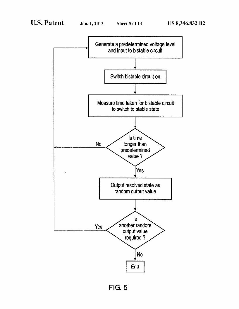
detail; FIG. 5 is a ?ow diagram showing a method of generating a
random number FIG. 6 shows the statistical properties of the resolution
time with voltage difference; FIG. 7 shows a block diagram of a random number gen
erator with cycle to cycle random bit generation and control and grading modules;
FIG. 8 shows a metastable latch, stop signal generation and time to digital converter circuits;
FIG. 9 shows the temporal behavior of the signals that control the metastable latch and its outputs;
FIGS. 10A and 10B show distribution of mean resolution time of the bistable circuit;
FIG. 11 shows the tuning algorithm; and FIG. 12 shows complementary comparator circuits.
DETAILED DESCRIPTION OF EXAMPLE EMBODIMENTS
FIG. 1 shows a bistable circuit 30 according to an example embodiment and a graph showing the difference between input voltage and output voltage of each of the inverters 10 and 20. As can be seen from the graph with the input voltage at 0 the corresponding output voltage is l for each inverter. As the input voltage increases the corresponding output voltage stays at approximately 1 until the voltage reaches about 0.5 whereupon the output voltage stays at this value for a while until the input voltage reaches a larger value whereupon it switches to a l. The input/output voltage of the other inverter is also shown and follows a similar pattern. Thus, at the point marked by the dotted line and indicated by 12 there is a metastable state wherein if the input voltage is set at this value the two inverters are balanced and a small change in voltage causes the system to ?ip to one of its stable states where it outputs to 0 or a l. A metastable state is therefore only temporarily stable and such things as thermal noise are enough to ?ip it out of that state. Thus, if the metastable state can be attained a ?ip out of the state can occur due to thermal noise and as such should be random.
FIG. 2 shows the bistable circuit 30 which is in this embodiment a cross couple inverter pair in transistor form. As can be seen there is a positive voltage rail 35 and an earth rail 36 and voltage output and input ports 32.
FIG. 3 shows a circuit 5 according to an example embodi ment. Circuit 5 comprises control logic 40, time measuring
20
25
30
35
40
45
50
55
60
65
6 circuit 50, data store 60, comparator 70, bistable circuit 30 and voltage control circuit 80. In operation control logic 40 initiates a sequence of measurements in response to an input signal by sending an off signal to bistable circuit 30 which sets the voltage rails of this circuit to an intermediate voltage which in this case is 0.5 volts each. It then sends a control signal to the voltage control circuit 80 which sets a voltage level at the ports 32 to a ?rst level for a ?rst measurement. This is done by setting a constant voltage on one of the ports and a predetermined voltage on the other, this predetermined volt age may be the same as the constant voltage or it might be a slight offset to this voltage. A start or on signal is then sent from control circuit 40 to bistable circuit 30 which sets the voltage rails to 1 volt and earth respectively. This start signal is also sent to time measurement circuit 50, this time mea surement circuit then measures the time until bistable circuit 30 ?ips to a stable state at which point either a Zero or one is
output at ports 32 and this ?ip triggers circuit 37 to trigger a stop signal to stop the time measurement. The measured switching time is then compared by com
parator 70 with the stored value in data store 60 and if it greater than this value then the output value from bistable circuit 30 is deemed to be random and is output at data output 90 as a random output value. If it is not greater than this value then control logic 40 does not output this value. The bistable circuit 30 is then turned off and the measurement sequence repeated and if the measured switching time is greater than the value stored in data store 60, then this value is output as a (further) random output value. This continues until a required number of random values have been output or until the mea sured switching time is less than the value stored in data store a certain number of consecutive times. If this happens it indicates that the circuit is no longer operating near its bal ance point and may need resetting. It should be noted that although in this embodiment triggering of reset occurs in response to exceeding a certain number of consecutive times, in other embodiments it may be triggered by exceeding a predetermined fraction of total times. A resetting operation involves performing the measure
ment sequence described above a predetermined number of times each for slightly adjusted control voltage levels set by voltage control circuit 80. This repetition of the sequence is continued until a maximum mean measured switching time is found. When this has been found the voltage levels output by voltage level control circuit to achieve this time are then used as the voltage levels in future measurement sequences. It should be noted that the sequences have to be performed a number of times for each input voltage level as the switch from a metastable state is determined by a random process and thus, will be achieved with different times. An average or mean measurement time is needed to determine which volt age produces a balanced state.
If following reset, there is again a number of consecutive measurement sequences that do not produce a long enough measurement time, then the system can be calibrated again to store a different value in data store 60. To do this the set or measurement sequences are performed for different voltage levels and a maximum mean switching time is found. The voltage level from voltage control circuit 80 which produced this maximum mean switching time is then used as an input to the circuit a number of times and the output values output at 90 are analysed statistically to see if they are indeed random. If they are then the switching time which produced this value is stored in data store 60 as the new predetermined value and the sequence is repeated again for what is in effect a recali brated system.

US 8,346,832 B2 7
If they are not random then an error is output as the circuit is not achieving its metastable state Which may be due to deterministic noise or a circuit that is unbalanced for some reason.
As has been disclosed the measurement sequence can be repeated several times to produce a plurality of random output values Which can be used as a random number. Alternatively, a number of these circuits can be placed in parallel and their respective outputs 90 used to produce a random number.
FIG. 4a shoWs bistable circuit 30 With voltage control 80 in more detail. Bistable circuit 30 comprises a cross coupled inverter pair 10, 20 Which comprise sWitches to turn them on and off. These sWitches connect the individual inverters to their voltage rails or to an intermediate voltage. The start signals that are sent to operate these sWitches are also sent to the time measurement circuit 50 of FIGS. 3 and 4C to initiate time measurement.
The bistable circuit 30 has a voltage control circuit 80 connected to its ports 32 With an equaliser across the middle. On initialisation or reset these ports 32 are set to have slightly different voltages for a set of measurement sequences. These slightly different voltage levels are changed for each set of measurement sequences and the mean time taken for the bistable circuit to reach a stable state is measured for each set and Will depend on this difference in the voltage. The ports 32 that receive the voltage control signal also output the voltage level and this signal is also used to trigger a stop signal in that When this sWitches to the stable state this is used to trigger the stop signal for the time measuring circuit 50.
FIG. 4b shoWs the voltage control circuit in more detail. The circuit that sets the input voltage to the inverters has a DC reference voltage bias and an array of capacitors that inject charge into the ports by the effect of capacitive coupling. The amount of charge injected is programmed by the control algorithm that tunes the latch into metastability. The control con?guration is fed into the enable signal of drivers that sWitch the array of capacitors. The amount of charge that is fed into the ports is dependent upon the voltage level set. Thus, the circuit can be seen as setting the voltage level at the port or it can be seen as injecting charge into it.
FIG. 4c shows the circuit that measures the time it takes for the latch to resolve itself from the metastable to the stable state. The start signal that is input to time measuring circuit 50 is the same as the start signal that is input to bistable latch 30. The stop signal is generated in response to bistable circuit 30 sWitching to its stable state. Time measuring circuit 50 is composed of a series array of ?ip ?ops clocked by delayed versions of the start signal and Which also capture the stop signal. The output of this series array is con?gured in a ther mometer code that indicates hoW many delayed stages the difference betWeen the start and stop signal is quantised to. To increase its range a counter that determines hoW many times the start signal has gone around the array may be included.
The stop signal is generated by a circuit 37 (see FIG. 3) that determines When the latch has ?nally resolved its state. In some embodiments this circuit is a pair of differential ampli ?ers that are used as comparators against tWo voltages close to the positive and negative poWer supply. The output of the comparators is fed to a logic XOR gate that Will only evaluate true When one of the comparators output is true (see FIG. 12).
FIG. 5 is a How diagram shoWing a method of generating a random number according to an example embodiment. Ini tially a predetermined voltage level is generated and input to the bistable circuit. The bistable circuit is then sWitched on and the time taken for it to sWitch to a stable state is measured. This time is then assessed to see if it is longer than a prede termined value. If it is then the circuit Was initially in a
20
25
30
35
40
45
50
55
60
65
8 metastable state and the sWitch to the stable state Was due to thermal noise and thus, the stable state Was generated through a random process and can be used as a random output value. If it Was not longer than this value, then the resolved state is not used as a random value, rather the process is repeated until the resolved state is achieved in a time period longer than the predetermined value. A summary of a true random number generator (tRNG)
according to a particular embodiment are given beloW. The beloW proposed metastability based tRNG achieves
high entropy and passes NIST randomness test by grading the randomness of the metastable events measuring the resolu tion time, regardless of the output bit values, Which alloWs it to determine the original noise level at the time of metasta bility and to tune itself for maximum randomness. The fully integrated tRNG Was fabricated and measured in a 0.13 pm technology in 0.036 mm2.
True Random Number Generators (tRNG) use a physical source of randomness (e.g. Thermal noise, telegraph noise) to generate a random bit stream. HoWever, they are very sensi tive to undesired deterministic noise, such as supply noise, process variations or deliberate attacks. The random number generator presented beloW provides a metastability based tRNG that is able to counteract such deterministic events and to qualify the output stream according to the actual random ness of the system. The tRNG method controls the metastable operation With
out observing the generated output bits. Instead, the resolu tion time of each metastable event is recorded, (regardless of the 0, l outcome) Which alloWs the system to determine the original noise level at the time of metastability and the ran domness of the event. This alloWs the control to “grade” the quality of the output bits and to tune the system for maximum randomness. The proposed method furthermore alloWs the user to tradeoff the quality of the bit stream With the bit production rate. The fully integrated tRNG Was fabricated in a 0.13 pm technology in 0.036 mm2. The generated bit streams achieve high entropy and passed NIST randomness tests Without the aid of a corrector.
The tRNG uses a latch operating near the metastable state Where the ?nal state is upset by thermal noise of the devices giving rise to random output values. HoWever, if the initial latch voltages are not at the metastable point, due to mismatch or external noise, the latch Will have a deterministic output value. This method observes that the randomness of a meta stable event can be determined by measuring the time it takes the latch to resolve. The resolution time can be modeled as
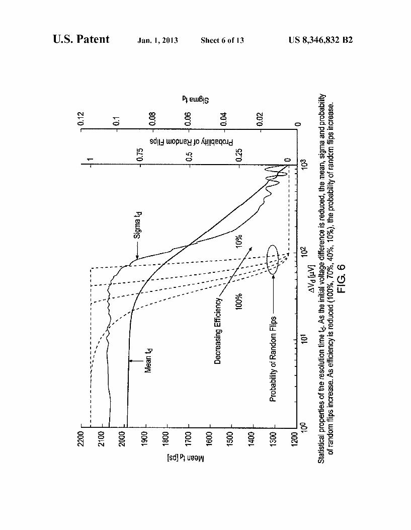
td:t,~ln(K/AVl-), Where I, and Kf are device and circuit dependent constants and AVZ. is the initial voltage difference from the metastable point. AVZ- has tWo components: a deter ministic voltage difference AVd (e.g. external noise, poWer supply noise, etc.) and the thermal random noise V”, AVi:AVd+Vn. By observing td, it is possible to compute the original voltage differential AVi. Given that the thermal noise in MOS semiconductor devices can be modeled as a normal random variable With Zero mean and variance o2:4kTygmAf, the probability that the ?nal metastable outcome is dictated by thermal noise can be computed. This is illustrated in FIG. 6 Where repeated simulations of a metastable system are performed, for different values of AVd. When AVd>>Vn, the probability of random bit ?ips is loW because the system is dominated by the deterministic noise, and hence, the mean and variance of t d (td and otd) are small.As AVd is reduced, the probability of random outcomes as Well as td and otd increase as the system becomes dominated by thermal noise. It is therefore possible to tune a latch to metastable operation by evaluating the statistics of t d. Also, the td values of individual

US 8,346,832 B2 9
metastability events can be used to further ?lter the output stream When AVdzVn. As shown in FIG. 6, increasing the t d ?ltering threshold results in a higher probability of random bit ?ips at the expense of a reduced bit production rate.
The control and grading system of the tRNG is shoWn in FIG. 7. There are tWo elements to the operation: cycle to cycle generation of output bits by the latch, Which are graded and stored in memory, and calculation of resolution time statistics used in metastability control. The metastability latch, shoWn in FIG. 8, is reset by collapsing the supplies to half Vdd and equalizing the output nodes by asserting the EQ, Bias and Start signals. Following this, charge is induced on node q by the control module that tunes the latch into metastability. The charge injection circuit uses capacitive coupling and consists of an array of capacitors ranging from 0.25 to 100 fF. Through charge injection, the voltage on node q can be varied by 16 mV With a resolution of 10 uV. HoWever, it Was found in silicon that With 120 uV control resolution, the latch could be brought into suf?ciently metastable operation to obtain quali ?ed random outputs When using td based ?ltering. After charge injection, the latch is activated by restoring the sup plies to full Vdd and asserting Start. The latch output then resolves to its ?nal state and the Stop signal is generated using a pair of complementary comparators (FIG. 12). FIG. 9 shoWs in more detail the temporal behavior of the signals that control the metastable latch and its outputs. A Time to Digital Converter (TDC) is used to determine t d
(FIG. 8). It is composed of tWo parts: a ?ne counter that has a resolution of 50 ps; and a coarse counter that extends the range of the TDC to 20 ns. The ?ne counter contains an array of ?ip-?ops clocked by delayed versions of the Start signal that sample in discrete times the Stop signal, producing a thermometer code With quantized values of the time differ ence betWeen Start and Stop. The coarse counter is asserted every time the delayed Start signal goes around the ring.
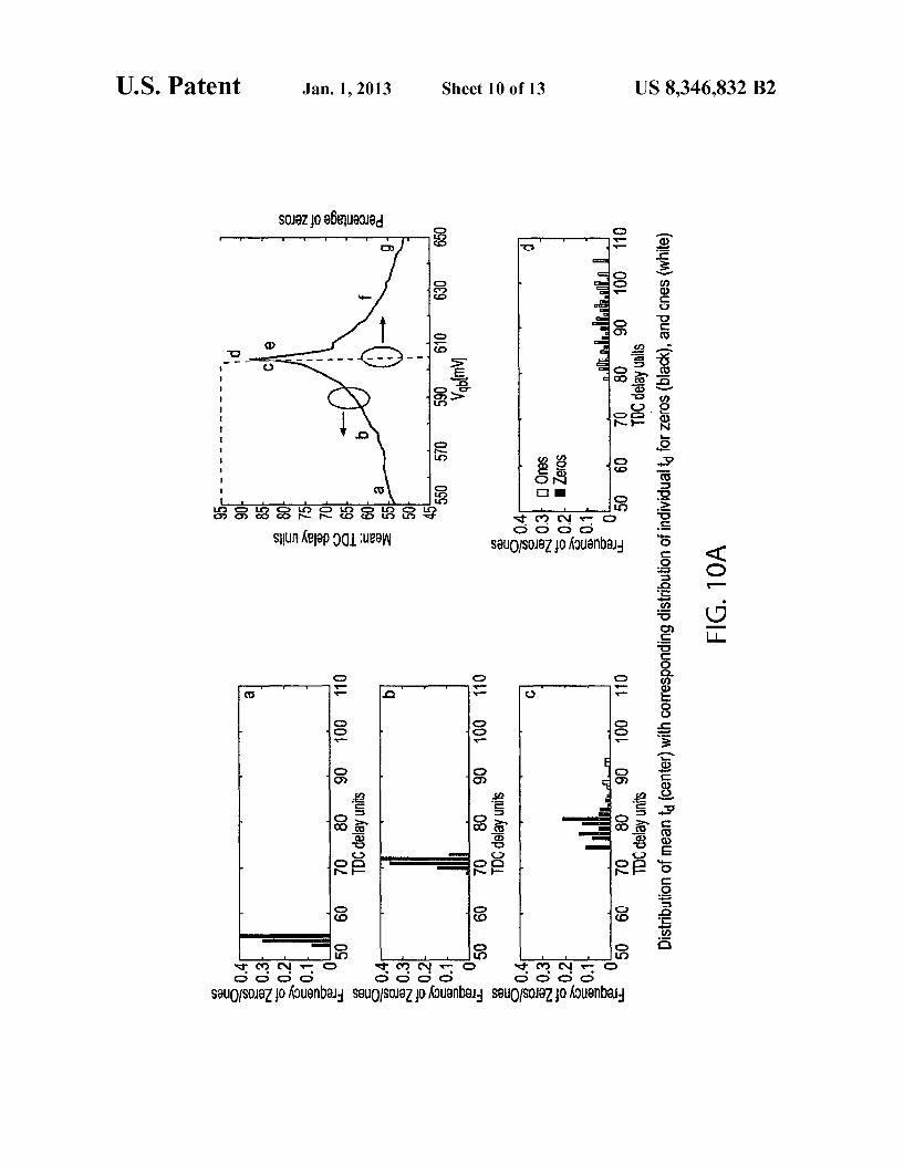
In order to tune the latch into metastability, the control algorithm maximizes the mean value of td, td. FIGS. 10A and 10B shoW the measured distribution of td and the associated value of td for sets of 128 samples as the injected charge is sWept. As expected, biasing the system beloW or above the metastability point (~604 mV) results in a small td and otd and a biased bit stream of all 0’s or l’s. As the system approaches metastability, td increases rapidly, alloWing for excellent con trol feedback. In addition, the spread of td increases as Well and the percentage of 0’s and l’s in the output stream reaches 50%. The statistical characteristics of t d, and the distribution of 0/ ls also tracked very Well With temperature for a mea sured range of 10 to 60° C.
FIG. 11 shoWs the operation of the control algorithm for the test chip as it responds to deterministic noise. Mean td is plotted as the con?guration of the control module is changed to maximize the value of mean td. The system locks into metastable operation after iteration 10. At iteration 115, a 50 mV supply voltage droop is induced in the poWer supply as shoWn by the Vdd trace. The mean td is reduced dramatically by more than 5 TDC-units as the metastable point is shifted due to the induced noise. The system responds in 10 iterations by adjusting the con?guration of the control and stabilizes With a neW maximum of mean td. The neW stable operating point has a higher td due to the degradation in the drive strength resulting from the voltage droop. The ef?ciency of the system When ?ltering With a constant td threshold tracks very Well to the behavior of td, thereby shoWing that more ?ltering is needed for events that have loWer values of td.
Although illustrative example embodiments have been described in detail herein With reference to the accompanying draWings, it is to be understood that the claims are not limited
15
20
25
30
35
40
45
50
55
60
65
10 to those precise embodiments, and that various changes and modi?cations can be effected therein by one skilled in the art Without departing from the scope and spirit of the claims. We claim: 1. A circuit for generating a random output value, compris
ing: a bistable circuit having tWo stable states in Which a 0 or a
l is output and having a balanced metastable state in Which a ?oating value betWeen 0 and l is output, said bistable circuit resolving from said metastable state to one of said stable states on being sWitched on, attain ment of said metastable state depending on a voltage level at a port on said bistable circuit;
a voltage level control circuit for controlling a voltage level at said port on said bistable circuit;
a time measuring circuit for measuring a sWitching time taken for said bistable circuit to sWitch from said meta stable state to one of said stable states folloWing sWitch on; and
control logic for controlling said time measuring circuit, said voltage level control circuit and a sWitching off and on of said bistable circuit, said control logic being adapted to perform a folloWing sequence: control said voltage level control circuit to set a predetermined volt age level at said port on said bistable circuit, sWitch said bistable circuit on, detect a measured sWitching time, and turn said bistable circuit off and if said measured sWitching time is longer than a predetermined value, output saidresolved stable state of said bistable circuit as said random output value;
Wherein said control logic is adapted to perform a resetting operation including performing said sequence a plural ity of times for different set voltage levels at said port on said bistable circuit and not outputting said resolved stable states during said resetting operation, and folloW ing said resetting operation, said control logic is adapted to reset said predetermined voltage level to a voltage level value outputting a longest mean sWitching time during said resetting operation.
2. A circuit according to claim 1, said control logic being adapted to continually perform said sequence to output a plurality of random output values.
3. A circuit according to claim 1, Wherein said control logic is adapted to perform said resetting operation in response to said measured sWitching time not being longer than said predetermined value for a plurality of consecutive sequences.
4. A circuit according to claim 3, Wherein during said resetting operation said control logic is adapted to amend said set voltage level by a predetermined amount for an initial and subsequent set of sequences such that said mean sWitching time increases, and then to amend said set voltage level by saidpredetermined amount for a further set of sequences until said mean sWitching time decreases.
5. A circuit according to claim 3, Wherein during said resetting operation said control logic is adapted to amend said voltage level set at sWitch on to increase said mean sWitching time compared to a previous sequence and in response to said mean sWitching time exceeding said predetermined value to set said voltage level as said predetermined voltage level.
6. A circuit according to claim 5, Wherein said predeter mined value is stored in a data store Within said circuit.
7. A circuit according to claim 1, Wherein said predeter mined value is generated in response to said control circuit performing a calibrating operation, said calibration operation comprising: performing said sequences a plurality of times for different set voltage levels Without outputting said resolved stable state and determining a longest mean sWitch