12-Bit High-Speed, Multiple SARs A/D Converter...
78
© 2014-2017 Microchip Technology Inc. DS70005213F-page 1 12-Bit High-Speed, Multiple SARs A/D Converter (ADC) HIGHLIGHTS This section of the manual contains the following major topics: 1.0 Introduction ....................................................................................................................... 2 2.0 Registers ........................................................................................................................... 5 3.0 Conversion Sequence..................................................................................................... 36 4.0 ADC Operation................................................................................................................ 36 5.0 Application Examples...................................................................................................... 57 6.0 Operation During Power-Saving Modes ......................................................................... 70 7.0 Effects of Reset ............................................................................................................... 70 8.0 Register Map................................................................................................................... 71 9.0 Related Application Notes............................................................................................... 75 10.0 Revision History .............................................................................................................. 76
Transcript of 12-Bit High-Speed, Multiple SARs A/D Converter...
12-Bit High-Speed, Multiple SARs A/D Converter (ADC)
HIGHLIGHTS
This section of the manual contains the following major topics:
1.0 Introduction ....................................................................................................................... 2
2.0 Registers........................................................................................................................... 5
3.0 Conversion Sequence..................................................................................................... 36
4.0 ADC Operation................................................................................................................ 36
5.0 Application Examples...................................................................................................... 57
6.0 Operation During Power-Saving Modes ......................................................................... 70
7.0 Effects of Reset............................................................................................................... 70
8.0 Register Map................................................................................................................... 71
9.0 Related Application Notes............................................................................................... 75
10.0 Revision History .............................................................................................................. 76
© 2014-2017 Microchip Technology Inc. DS70005213F-page 1
dsPIC33/PIC24 Family Reference Manual
1.0 INTRODUCTION
The dsPIC33/PIC24 12-Bit High-Speed, Multiple SARs Analog-to-Digital Converter (ADC)includes the following features:
• Multiple ADC Cores:
- Multiple single channel dedicated ADC cores (depending on the specific device implementation)
- One shared (common) ADC core
• Configurable 6, 8, 10 or 12-Bit Resolution for each ADC Core
• Up to 3.25 Msps Conversion Rate per Channel for 12-Bit Resolution
• Up to 32 Analog Input Sources (depending on the specific device implementation)
• Single-Ended or Pseudodifferential Inputs on a per Channel Basis for All Channels
• Conversion Result can be Formatted as Unsigned or Signed Data on a per Channel Basis for All Channels
• Separate 16-Bit Conversion Result Register for each Analog Input
• Early Interrupt Generation to enable Fast Processing of Converted Data
• Multiple Integrated Digital Comparators (depending on the specific device implementation):
- Multiple comparison options
- Assignable to specific analog inputs
• Multiple Oversampling Filters (depending on the specific device implementation):
- Provides increased resolution
- Assignable to a specific analog input
• Operation during CPU Sleep and Idle modes
• Hardware Capacitive Voltage Divider (CVD) to Measure Capacitance Connected to the Input
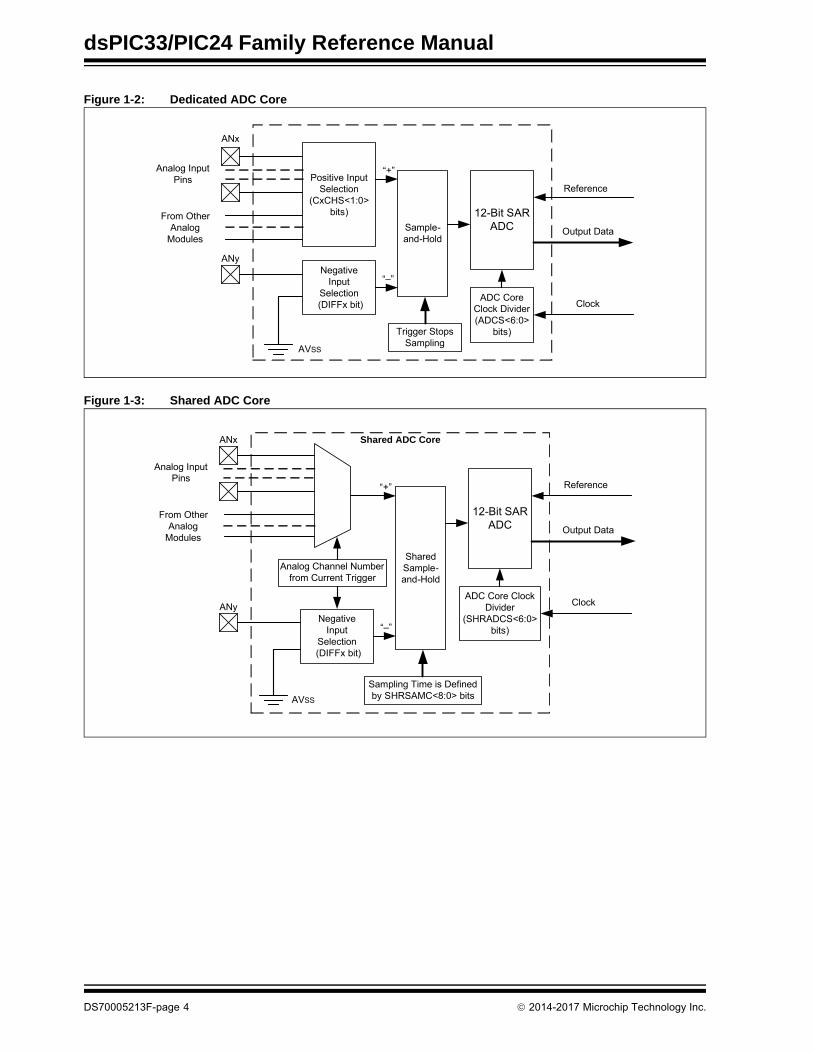
Simplified block diagrams of the Multiple SARs 12-Bit ADC are illustrated in Figure 1-1,Figure 1-2 and Figure 1-3.
The module consists of a few independent SAR ADC cores. The analog inputs (channels) areconnected through multiplexers and switches to the Sample-and-Hold (S/H) circuit of each ADCcore. The core uses the channel information (output format, Measurement mode and inputnumber) to process the analog sample. When conversion is complete, the result is stored in theresult buffer for the specific analog input, and passed to the digital filter and digital comparator ifthey were configured to use data from this particular channel.
Note: This family reference manual section is meant to serve as a complement to devicedata sheets. Depending on the device variant, this manual section may not apply toall dsPIC33/PIC24 devices. Please consult the note at the beginning of the chapterin the specific device data sheet to check whether this document supports thedevice you are using.
Device data sheets and family reference manual sections are available fordownload from the Microchip Worldwide Web site at: http://www.microchip.com.
DS70005213F-page 2 2014-2017 Microchip Technology Inc.

12-Bit High-Speed, Multiple SARs A/D Converter (ADC)
Figure 1-1: 12-Bit High-Speed, Multiple SARs ADC Block Diagram
Dedicated ADC Core 0
(see Figure 1-2)
Reference Voltage Selection(REFSEL<2:0> bits)
Clock Source Selection(CLKSEL<1:0> bits)
Clock Source Divider(CLKDIV<5:0> bits)
AVDD AVSS VREF+ VREF- INTREF
Instruction Clock
FRC AUX Clock
Reference
Reference
Reference
Output Data
Clock
Clock
Clock
Output Data
Output Data
Digital Comparator 0ADCMP0Interrupt
Digital Comparator xADCMPxInterrupt
Digital Filter 0
Digital Filter x
ADFL0DAT
ADFLxDAT
ADCBUF0
ADCBUF1
ADCBUFx
ADCAN0Interrupt
ADCAN1Interrupt
ADCANxInterrupt
ADFL0Interrupt
ADFLxInterrupt
Dedicated ADC Core 1
(see Figure 1-2)
Shared ADC Core(see Figure 1-3)
Analog Inputs
Analog Inputs
Analog Inputs
Fosc
(See Figure 1-2)
(See Figure 1-2)
(See Figure 1-3)
2014-2017 Microchip Technology Inc. DS70005213F-page 3
dsPIC33/PIC24 Family Reference Manual
Figure 1-2: Dedicated ADC Core
Figure 1-3: Shared ADC Core
Sample-and-Hold
12-Bit SAR ADC
Positive Input Selection
(CxCHS<1:0> bits)
NegativeInput
Selection(DIFFx bit)
Analog Input Pins
From Other Analog
Modules
AVSS
ANx
ANy
“+”
“–”
ADC Core Clock Divider(ADCS<6:0>
bits)
Reference
Output Data
Clock
Trigger Stops Sampling
SharedSample-and-Hold
Shared ADC Core
NegativeInput
Selection(DIFFx bit)
Analog Input Pins
From Other Analog
Modules
AVSS
“+”
“–”
Analog Channel Number from Current Trigger
ANx
ANy
12-Bit SAR ADC
ADC Core Clock Divider
(SHRADCS<6:0> bits)
Reference
Clock
Output Data
Sampling Time is Defined by SHRSAMC<8:0> bits
DS70005213F-page 4 2014-2017 Microchip Technology Inc.

12-Bit High-Speed, Multiple SARs A/D Converter (ADC)
2.0 REGISTERS
The Special Function Registers (SFRs) of the 12-Bit High-Speed, Multiple SARs ADC moduleare divided into two groups: control registers and data registers. A complete list of all SFRsimplemented by the ADC is provided in Table 8-1.
2.1 Control Registers
The ADCON1L register (Register 2-1) contains bits to enable the module, define the modulebehavior in Idle mode and enable the CVD feature.
The ADCON1H register (Register 2-2) controls the output data format and the shared ADC coreresolution.
The ADCON2L register (Register 2-3) controls the clock divider and early interrupt timingselection for the shared ADC core. It has bits to enable the common interrupt for the eventsrelated to the voltage reference and a bit to enable an early interrupt feature for the individualinput channels.
The ADCON2H register (Register 2-4) controls the sampling time for the shared ADC core. Italso provides the status bits, which indicate that the module voltage reference is ready foroperation. This register allows adjusting the internal capacitance value for the CVD feature.
The ADCON3L register (Register 2-5) selects the voltage reference for all ADC cores andcontrols common, level and single-shot software triggers. Also, it has control bits to suspend alltriggers for the module.
The ADCON3H register (Register 2-6) has bits to enable all ADC cores and select a clock sourcefor the module. Also, this register controls the module clock source divider.
The ADCON4L register (Register 2-7) allows enabling a delay between trigger and conversionfor the dedicated ADC cores, and triggers synchronization.
The ADCON4H register (Register 2-8) selects channels for the dedicated ADC cores.
The ADCON5L register (Register 2-9) controls power for all ADC cores.
The ADCON5H register (Register 2-10) has bits to enable a common interrupt for each ADC corewhen it is powered on and ready for operation. Also in this register, the power-on delay isspecified for all ADC cores.
The ADCOREnL (where ‘n’ is a dedicated ADC core number) registers (Register 2-11) define adelay between trigger and conversion for each dedicated ADC core.
The ADCOREnH (where ‘n’ is a dedicated ADC core number) registers (Register 2-12) defineresolution, early interrupt time selection and the ADC core clock divider for each dedicated ADC core.
The ADLVLTRGL and ADLVLTRGH registers (Register 2-13 and Register 2-14) have bits toselect either the level-sensitive trigger or the edge-sensitive trigger for each input channel.
The ADEIEL and ADEIEH registers (Register 2-15 and Register 2-16) have bits to enable theearly interrupts generation for each input channel.
The ADEISTATL and ADEISTATH registers (Register 2-17 and Register 2-18) contain the earlyinterrupts status flags for each input channel.
The ADMOD0L, ADMOD0H, ADMOD1L and ADMOD1H registers (Register 2-19 throughRegister 2-22) have bits to enable the Pseudodifferential mode and signed output data format foreach input channel.
The ADIEL and ADIEH registers (Register 2-23 and Register 2-24) have bits to enable theindividual and common interrupts for each input channel.
The ADSTATL and ADSTATH registers (Register 2-25 and Register 2-26) contain the data readyflags for each input channel.
The ADTRIGnL and ADTRIGnH registers (Register 2-27) define a trigger source for each inputchannel.
The ADCAL0L, ADCAL0H, ADCAL1L and ADCAL1H registers (Register 2-28 throughRegister 2-31) control the calibration for each ADC core. The calibration is not required for somedevices. Refer to the specific device data sheet to see if these registers are implemented.
2014-2017 Microchip Technology Inc. DS70005213F-page 5

dsPIC33/PIC24 Family Reference Manual
The ADCMPnCON registers (Register 2-32) control the operation of the digital comparators,including the generation of the interrupts and the comparison criteria to be used. These registersalso provide the status when a comparator event occurs. One register is provided for each digitalcomparator.
The ADCMPnENL and ADCMPnENH registers (Register 2-33 and Register 2-34) select whichof the analog input conversion results are to be processed by the digital comparator. One pair(L and H) is provided for each digital comparator.
The ADFLnCON registers (Register 2-35) control the operation of the oversampling filters andprovide status bits for the filters’ operation. One register is provided for each oversampling filter.The ADCSSL and ADCSSH registers (Register 2-36 and Register 2-37) select which of theanalog inputs are to be scanned/processed by the CVD.
2.2 Data Registers
The ADCBUFx registers store the output data of the Analog-to-Digital conversion. In general,there is one register provided for each of the implemented analog channels; each channel willhave a corresponding numbered ADCBUFx register. Although the registers are 16 bits wide, theusage of the registers for storing the 12-bit conversion results is determined by the selected dataoutput format. See Section 4.10 “Conversion Result” for more information.
The ADCMPnLO and ADCMPnHI registers store the 16-bit high and low digital comparisonvalues for use by the digital comparators. One pair (HI and LO) is provided for each ADCcomparator.
The ADFLnDAT registers contain the 16-bit output data from the oversampling filters. There isone register for each oversampling filter.
The ADCVDDAT register contains the 16-bit output data from the Capacitive Voltage Divider(CVD). This register may not be implemented on some devices. Refer to the specific device datasheet to see if the CVD feature is implemented on the device.
DS70005213F-page 6 2014-2017 Microchip Technology Inc.

12-Bit High-Speed, Multiple SARs A/D Converter (ADC)
Register 2-1: ADCON1L: ADC Control Register 1 Low
R/W-0 U-0 R/W-0 U-0 R/W-0 U-0 U-0 U-0
ADON(1) — ADSIDL — CVDEN(2) — — —
bit 15 bit 8
R/W-0 U-0 U-0 U-0 U-0 U-0 U-0 U-0
NRE(3) — — — — — — —
bit 7 bit 0
Legend:
R = Readable bit W = Writable bit U = Unimplemented bit, read as ‘0’
-n = Value at POR ‘1’ = Bit is set ‘0’ = Bit is cleared x = Bit is unknown
bit 15 ADON: ADC Enable bit(1)
1 = ADC module is enabled0 = ADC module is off
bit 14 Unimplemented: Read as ‘0’
bit 13 ADSIDL: ADC Stop in Idle Mode bit
1 = Discontinues module operation when device enters Idle mode0 = Continues module operation in Idle mode
bit 12 Unimplemented: Read as ‘0’
bit 11 CVDEN: CVD Enable bit(2)
1 = CVD is enabled0 = CCD is off
bit 10-8 Unimplemented: Read as ‘0’
bit 7 NRE: Noise Reduction Enable bit(3)
1 = Holds conversion process for 1 TADCORE when another core completes conversion to reduce noisebetween cores
0 = Noise Reduction feature is disabled
bit 6-0 Unimplemented: Read as ‘0’
Note 1: Set the ADON bit only after the ADC module has been configured. Changing ADC Configuration bits when ADON = 1 will result in unpredictable behavior.
2: The CVD feature is not available on all devices and the CVDEN bit may not be implemented. Refer to the device data sheet for more information.
3: The Noise Reduction feature is not available on all devices and the NRE bit may not be implemented. Refer to the device data sheet for more information.
2014-2017 Microchip Technology Inc. DS70005213F-page 7

dsPIC33/PIC24 Family Reference Manual
Register 2-2: ADCON1H: ADC Control Register 1 High
r-0 r-0 r-0 r-0 r-0 r-0 r-0 r-0
— — — — — — — —
bit 15 bit 8
R/W-0 R/W-1 R/W-1 r-0 r-0 r-0 r-0 r-0
FORM SHRRES1 SHRRES0 — — — — —
bit 7 bit 0
Legend: r = Reserved bit
R = Readable bit W = Writable bit U = Unimplemented bit, read as ‘0’
-n = Value at POR ‘1’ = Bit is set ‘0’ = Bit is cleared x = Bit is unknown
bit 15-8 Reserved: Must be written as ‘0’
bit 7 FORM: Fractional Data Output Format bit
1 = Fractional0 = Integer
bit 6-5 SHRRES<1:0>: Shared ADC Core Resolution Selection bits
11 = 12-bit resolution10 = 10-bit resolution01 = 8-bit resolution00 = 6-bit resolution
bit 4-0 Reserved: Must be written as ‘0’
DS70005213F-page 8 2014-2017 Microchip Technology Inc.

12-Bit High-Speed, Multiple SARs A/D Converter (ADC)
Register 2-3: ADCON2L: ADC Control Register 2 Low
R/W-0 R/W-0 r-0 R/W-0 r-0 R/W-0 R/W-0 R/W-0
REFCIE REFERCIE(2) — EIEN — SHREISEL2(1) SHREISEL1(1) SHREISEL0(1)
bit 15 bit 8
U-0 R/W-0 R/W-0 R/W-0 R/W-0 R/W-0 R/W-0 R/W-0
— SHRADCS6 SHRADCS5 SHRADCS4 SHRADCS3 SHRADCS2 SHRADCS1 SHRADCS0
bit 7 bit 0
Legend: r = Reserved bit
R = Readable bit W = Writable bit U = Unimplemented bit, read as ‘0’
-n = Value at POR ‘1’ = Bit is set ‘0’ = Bit is cleared x = Bit is unknown
bit 15 REFCIE: Band Gap and Reference Voltages Ready Common Interrupt Enable bit
1 = Common interrupt will be generated when band gap and reference voltage are ready0 = Common interrupt is disabled for band gap and reference voltage ready event
bit 14 REFERCIE: Band Gap and Reference Voltages Error Common Interrupt Enable bit(2)
1 = Common interrupt will be generated when band gap or reference voltage error is detected0 = Common interrupt is disabled for band gap and reference voltages error event
bit 13 Reserved: Must be written as ‘0’
bit 12 EIEN: Early Interrupts Enable bit
1 = The early interrupt feature is enabled for the input channel interrupts (when the EISTATx flag is set)0 = The individual interrupts are generated when the conversion is done (when the ANxRDY flag is set)
bit 11 Reserved: Must be written as ‘0’
bit 10-8 SHREISEL<2:0>: Shared Core Early Interrupt Time Selection bits(1)
111 = Early interrupt is generated 8 TADCORE clocks prior to when the data is ready110 = Early interrupt is generated 7 TADCORE clocks prior to when the data is ready101 = Early interrupt is generated 6 TADCORE clocks prior to when the data is ready100 = Early interrupt is generated 5 TADCORE clocks prior to when the data is ready011 = Early interrupt is generated 4 TADCORE clocks prior to when the data is ready010 = Early interrupt is generated 3 TADCORE clocks prior to when the data is ready001 = Early interrupt is generated 2 TADCORE clocks prior to when the data is ready000 = Early interrupt is generated 1 TADCORE clock prior to when the data is ready
bit 7 Unimplemented: Read as ‘0’
bit 6-0 SHRADCS<6:0>: Shared ADC Core Input Clock Divider bits
These bits determine the number of TCORESRC (Source Clock Periods) for one shared TADCORE (CoreClock Period).1111111 = 254 source clock periods•••0000011 = 6 source clock periods0000010 = 4 source clock periods0000001 = 2 source clock periods0000000 = 2 source clock periods
Note 1: For the 6-bit shared ADC core resolution (SHRRES<1:0> = 00), the SHREISEL<2:0> settings, from ‘100’ to ‘111’, are not valid and should not be used. For the 8-bit shared ADC core resolution (SHRRES<1:0> = 01), the SHREISEL<2:0> settings, ‘110’ and ‘111’, are not valid and should not be used.
2: To avoid false interrupts, the REFERCIE bit must be set only after the module is enabled (ADON = 1).
2014-2017 Microchip Technology Inc. DS70005213F-page 9
dsPIC33/PIC24 Family Reference Manual
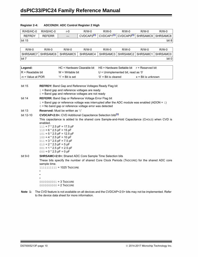
Register 2-4: ADCON2H: ADC Control Register 2 High
R/HS/HC-0 R/HS/HC-0 r-0 R/W-0 R/W-0 R/W-0 R/W-0 R/W-0
REFRDY REFERR — CVDCAP2(1) CVDCAP1(1) CVDCAP0(1) SHRSAMC9 SHRSAMC8
bit 15 bit 8
R/W-0 R/W-0 R/W-0 R/W-0 R/W-0 R/W-0 R/W-0 R/W-0
SHRSAMC7 SHRSAMC6 SHRSAMC5 SHRSAMC4 SHRSAMC3 SHRSAMC2 SHRSAMC1 SHRSAMC0
bit 7 bit 0
Legend: HC = Hardware Clearable bit HS = Hardware Settable bit r = Reserved bit
R = Readable bit W = Writable bit U = Unimplemented bit, read as ‘0’
-n = Value at POR ‘1’ = Bit is set ‘0’ = Bit is cleared x = Bit is unknown
bit 15 REFRDY: Band Gap and Reference Voltages Ready Flag bit
1 = Band gap and reference voltages are ready 0 = Band gap and reference voltages are not ready
bit 14 REFERR: Band Gap or Reference Voltage Error Flag bit
1 = Band gap or reference voltage was interrupted after the ADC module was enabled (ADON = 1)0 = No band gap or reference voltage error was detected
bit 13 Reserved: Must be written as ‘0’
bit 12-10 CVDCAP<2:0>: CVD Additional Capacitance Selection bits(1)
This capacitance is added to the shared core Sample-and-Hold Capacitance (CHOLD) when CVD isenabled.111 = 7 * 2.5 pF = 17.5 pF110 = 6 * 2.5 pF = 15 pF101 = 5 * 2.5 pF = 12.5 pF100 = 4 * 2.5 pF = 10 pF011 = 3 * 2.5 pF = 7.5 pF010 = 2 * 2.5 pF = 5 pF001 = 1 * 2.5 pF = 2.5 pF000 = 0 * 2.5 pF = 0 pF
bit 9-0 SHRSAMC<2:0>: Shared ADC Core Sample Time Selection bits
These bits specify the number of shared Core Clock Periods (TADCORE) for the shared ADC coresample time.1111111111 = 1025 TADCORE
•••0000000001 = 3 TADCORE
0000000000 = 2 TADCORE
Note 1: The CVD feature is not available on all devices and the CVDCAP<2:0> bits may not be implemented. Refer to the device data sheet for more information.
DS70005213F-page 10 2014-2017 Microchip Technology Inc.
12-Bit High-Speed, Multiple SARs A/D Converter (ADC)
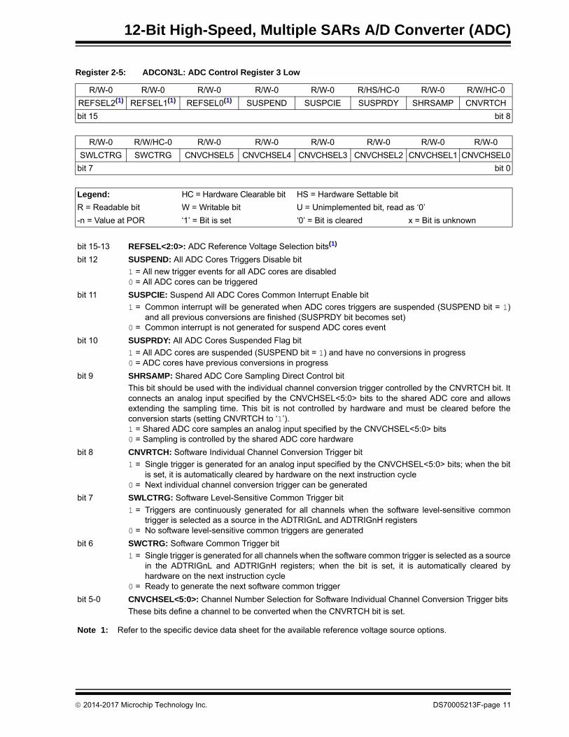
Register 2-5: ADCON3L: ADC Control Register 3 Low
R/W-0 R/W-0 R/W-0 R/W-0 R/W-0 R/HS/HC-0 R/W-0 R/W/HC-0
REFSEL2(1) REFSEL1(1) REFSEL0(1) SUSPEND SUSPCIE SUSPRDY SHRSAMP CNVRTCH
bit 15 bit 8
R/W-0 R/W/HC-0 R/W-0 R/W-0 R/W-0 R/W-0 R/W-0 R/W-0
SWLCTRG SWCTRG CNVCHSEL5 CNVCHSEL4 CNVCHSEL3 CNVCHSEL2 CNVCHSEL1 CNVCHSEL0
bit 7 bit 0
Legend: HC = Hardware Clearable bit HS = Hardware Settable bit
R = Readable bit W = Writable bit U = Unimplemented bit, read as ‘0’
-n = Value at POR ‘1’ = Bit is set ‘0’ = Bit is cleared x = Bit is unknown
bit 15-13 REFSEL<2:0>: ADC Reference Voltage Selection bits(1)
bit 12 SUSPEND: All ADC Cores Triggers Disable bit
1 = All new trigger events for all ADC cores are disabled0 = All ADC cores can be triggered
bit 11 SUSPCIE: Suspend All ADC Cores Common Interrupt Enable bit
1 = Common interrupt will be generated when ADC cores triggers are suspended (SUSPEND bit = 1)and all previous conversions are finished (SUSPRDY bit becomes set)
0 = Common interrupt is not generated for suspend ADC cores event
bit 10 SUSPRDY: All ADC Cores Suspended Flag bit
1 = All ADC cores are suspended (SUSPEND bit = 1) and have no conversions in progress0 = ADC cores have previous conversions in progress
bit 9 SHRSAMP: Shared ADC Core Sampling Direct Control bit
This bit should be used with the individual channel conversion trigger controlled by the CNVRTCH bit. Itconnects an analog input specified by the CNVCHSEL<5:0> bits to the shared ADC core and allowsextending the sampling time. This bit is not controlled by hardware and must be cleared before theconversion starts (setting CNVRTCH to ‘1’). 1 = Shared ADC core samples an analog input specified by the CNVCHSEL<5:0> bits0 = Sampling is controlled by the shared ADC core hardware
bit 8 CNVRTCH: Software Individual Channel Conversion Trigger bit
1 = Single trigger is generated for an analog input specified by the CNVCHSEL<5:0> bits; when the bitis set, it is automatically cleared by hardware on the next instruction cycle
0 = Next individual channel conversion trigger can be generated
bit 7 SWLCTRG: Software Level-Sensitive Common Trigger bit
1 = Triggers are continuously generated for all channels when the software level-sensitive commontrigger is selected as a source in the ADTRIGnL and ADTRIGnH registers
0 = No software level-sensitive common triggers are generated
bit 6 SWCTRG: Software Common Trigger bit
1 = Single trigger is generated for all channels when the software common trigger is selected as a sourcein the ADTRIGnL and ADTRIGnH registers; when the bit is set, it is automatically cleared byhardware on the next instruction cycle
0 = Ready to generate the next software common trigger
bit 5-0 CNVCHSEL<5:0>: Channel Number Selection for Software Individual Channel Conversion Trigger bits
These bits define a channel to be converted when the CNVRTCH bit is set.
Note 1: Refer to the specific device data sheet for the available reference voltage source options.
2014-2017 Microchip Technology Inc. DS70005213F-page 11

dsPIC33/PIC24 Family Reference Manual
Register 2-6: ADCON3H: ADC Control Register 3 High
R/W-0 R/W-0 R/W-0 R/W-0 R/W-0 R/W-0 R/W-0 R/W-0
CLKSEL1(1) CLKSEL0(1) CLKDIV5 CLKDIV4 CLKDIV3 CLKDIV2 CLKDIV1 CLKDIV0
bit 15 bit 8
R/W-0 R/W-0 R/W-0 R/W-0 R/W-0 R/W-0 R/W-0 R/W-0
SHREN C6EN(2) C5EN(2) C4EN(2) C3EN(2) C2EN(2) C1EN(2) C0EN(2)
bit 7 bit 0
Legend:
R = Readable bit W = Writable bit U = Unimplemented bit, read as ‘0’
-n = Value at POR ‘1’ = Bit is set ‘0’ = Bit is cleared x = Bit is unknown
bit 15-14 CLKSEL<1:0>: ADC Module Clock Source Selection bits(1)
bit 13-8 CLKDIV<5:0>: ADC Module Clock Source Divider bits
The divider forms a TCORESRC clock used by all ADC cores (shared and dedicated) from the TSRC ADCmodule clock source selected by the CLKSEL<1:0> bits. Then, each ADC core individually divides theTCORESRC clock to get a core-specific TADCORE clock, using the ADCS<6:0> bits in the ADCOREnHregister, or the SHRADCS<6:0> bits in the ADCON2L register. 111111 = 64 source clock periods•••000011 = 4 source clock periods000010 = 3 source clock periods000001 = 2 source clock periods000000 = 1 source clock period
bit 7 SHREN: Shared ADC Core Enable bit
This bit does not disable the core clock and analog bias circuitry.1 = Shared ADC core is enabled0 = Shared ADC core is disabled
bit 6-0 C6EN:C0EN: Dedicated ADC Core x Enable bits(2)
This bit does not disable the core clock and analog bias circuitry.1 = Dedicated ADC Core x is enabled0 = Dedicated ADC Core x is disabled
Note 1: Refer to the specific device data sheet for the available ADC module clock source options.
2: The number of the available dedicated ADC cores is device-specific and some CxEN bits may not be implemented. Refer to the device data sheet for more information.
DS70005213F-page 12 2014-2017 Microchip Technology Inc.

12-Bit High-Speed, Multiple SARs A/D Converter (ADC)
Register 2-7: ADCON4L: ADC Control Register 4 Low
U-0 r-0 r-0 r-0 r-0 r-0 r-0 r-0
— — — — — — — —
bit 15 bit 8
U-0 R/W-0 R/W-0 R/W-0 R/W-0 R/W-0 R/W-0 R/W-0
— SAMC6EN(1) SAMC5EN(1) SAMC4EN(1) SAMC3EN(1) SAMC2EN(1) SAMC1EN(1) SAMC0EN(1)
bit 7 bit 0
Legend: r = Reserved bit
R = Readable bit W = Writable bit U = Unimplemented bit, read as ‘0’
-n = Value at POR ‘1’ = Bit is set ‘0’ = Bit is cleared x = Bit is unknown
bit 15 Unimplemented: Read as ‘0’
bit 14-8 Reserved: Must be written as ‘0’
bit 7 Unimplemented: Read as ‘0’
bit 6-0 SAMC6EN:SAMC0EN: Dedicated ADC Core x Conversion Delay Enable bits(1)
1 = After the trigger, the conversion will be delayed and the ADC core will continue sampling during thetime specified by the SAMC<9:0> bits in the ADCOREnL register
0 = After the trigger, the sampling will be stopped immediately and the conversion will be started on thenext core clock cycle
Note 1: The number of available dedicated ADC cores is device-specific and some SAMCxEN bits may not be implemented. Refer to the device data sheet for more information.
2014-2017 Microchip Technology Inc. DS70005213F-page 13

dsPIC33/PIC24 Family Reference Manual
Register 2-8: ADCON4H: ADC Control Register 4 High
U-0 U-0 R/W-0 R/W-0 R/W-0 R/W-0 R/W-0 R/W-0
— — C6CHS1(1) C6CHS0(1) C5CHS1(1) C5CHS0(1) C4CHS1(1) C4CHS0(1)
bit 15 bit 8
R/W-0 R/W-0 R/W-0 R/W-0 R/W-0 R/W-0 R/W-0 R/W-0
C3CHS1(1) C3CHS0(1) C2CHS1(1) C2CHS0(1) C1CHS1(1) C1CHS0(1) C0CHS1(1) C0CHS0(1)
bit 7 bit 0
Legend:
R = Readable bit W = Writable bit U = Unimplemented bit, read as ‘0’
-n = Value at POR ‘1’ = Bit is set ‘0’ = Bit is cleared x = Bit is unknown
bit 15-14 Unimplemented: Read as ‘0’
bit 13-12 C6CHS<1:0>: Dedicated ADC Core 6 Input Channel Selection bits(1)
bit 11-10 C5CHS<1:0>: Dedicated ADC Core 5 Input Channel Selection bits(1)
bit 9-8 C4CHS<1:0>: Dedicated ADC Core 4 Input Channel Selection bits(1)
bit 7-6 C3CHS<1:0>: Dedicated ADC Core 3 Input Channel Selection bits(1)
bit 5-4 C2CHS<1:0>: Dedicated ADC Core 2 Input Channel Selection bits(1)
bit 3-2 C1CHS<1:0>: Dedicated ADC Core 1 Input Channel Selection bits(1)
bit 1-0 C0CHS<1:0>: Dedicated ADC Core 0 Input Channel Selection bits(1)
Note 1: The number of available dedicated ADC cores and input channel options for each ADC core are device-specific. Some CxCHS<1:0> bits may not be implemented. Refer to the device data sheet for the available ADC cores and their input channel options.
DS70005213F-page 14 2014-2017 Microchip Technology Inc.

12-Bit High-Speed, Multiple SARs A/D Converter (ADC)
Register 2-9: ADCON5L: ADC Control Register 5 Low
R/HC/HS-0 R/HC/HS-0 R/HC/HS-0 R/HC/HS-0 R/HC/HS-0 R/HC/HS-0 R/HC/HS-0 R/HC/HS-0
SHRRDY C6RDY(1) C5RDY(1) C4RDY(1) C3RDY(1) C2RDY(1) C1RDY(1) C0RDY(1)
bit 15 bit 8
R/W-0 R/W-0 R/W-0 R/W-0 R/W-0 R/W-0 R/W-0 R/W-0
SHRPWR C6PWR(1) C5PWR(1) C4PWR(1) C3PWR(1) C2PWR(1) C1PWR(1) C0PWR(1)
bit 7 bit 0
Legend: HC = Hardware Clearable bit HS = Hardware Settable bit
R = Readable bit W = Writable bit U = Unimplemented bit, read as ‘0’
-n = Value at POR ‘1’ = Bit is set ‘0’ = Bit is cleared x = Bit is unknown
bit 15 SHRRDY: Shared ADC Core Ready Flag bit
1 = ADC core is powered and ready for operation0 = ADC core is not ready for operation
bit 14-8 C6RDY:C0RDY: Dedicated ADC Core x Ready Flag bits(1)
1 = ADC core is powered and ready for operation0 = ADC core is not ready for operation
bit 7 SHRPWR: Shared ADC Core Power Enable bit
1 = ADC core is powered0 = ADC core is off
bit 6-0 C6PWR:C0PWR: Dedicated ADC Core x Power Enable bits(1)
1 = ADC core is powered0 = ADC core is off
Note 1: The number of available dedicated ADC cores is device-specific. Some CxRDY and CxPWR bits may not be implemented. Refer to the device data sheet for the available ADC cores.
2014-2017 Microchip Technology Inc. DS70005213F-page 15

dsPIC33/PIC24 Family Reference Manual
Register 2-10: ADCON5H: ADC Control Register 5 High
U-0 U-0 U-0 U-0 R/W-0 R/W-0 R/W-0 R/W-0
— — — — WARMTIME3 WARMTIME2 WARMTIME1 WARMTIME0
bit 15 bit 8
R/W-0 R/W-0 R/W-0 R/W-0 R/W-0 R/W-0 R/W-0 R/W-0
SHRCIE C6CIE(1) C5CIE(1) C4CIE(1) C3CIE(1) C2CIE(1) C1CIE(1) C0CIE(1)
bit 7 bit 0
Legend:
R = Readable bit W = Writable bit U = Unimplemented bit, read as ‘0’
-n = Value at POR ‘1’ = Bit is set ‘0’ = Bit is cleared x = Bit is unknown
bit 15-12 Unimplemented: Read as ‘0’
bit 11-8 WARMTIME<3:0>: ADC Cores Power-up Delay bits
These bits determine the power-up delay in the number of the Core Clock Source periods (TCORESRC) forall ADC cores.1111 = 32768 source clock periods1110 = 16384 source clock periods1101 = 8192 source clock periods1100 = 4096 source clock periods1011 = 2048 source clock periods1010 = 1024 source clock periods1001 = 512 source clock periods1000 = 256 source clock periods0111 = 128 source clock periods0110 = 64 source clock periods0101 = 32 source clock periods0000-0100 = 16 source clock periods
bit 7 SHRCIE: Shared ADC Core Ready Common Interrupt Enable bit
1 = Common interrupt will be generated when the ADC core is powered and ready for operation0 = Common interrupt is disabled for the ADC core ready event
bit 6-0 C6CIE:C0CIE: Dedicated ADC Core x Ready Common Interrupt Enable bits(1)
1 = Common interrupt will be generated when the ADC core is powered and ready for operation0 = Common interrupt is disabled for the ADC core ready event
Note 1: The number of available dedicated ADC cores is device-specific. Some CxCIE bits may not be implemented. Refer to the device data sheet for the available ADC cores.
DS70005213F-page 16 2014-2017 Microchip Technology Inc.

12-Bit High-Speed, Multiple SARs A/D Converter (ADC)
Register 2-11: ADCOREnL: Dedicated ADC Core n Control Register Low(1)
U-0 U-0 U-0 U-0 U-0 U-0 R/W-0 R/W-0
— — — — — — SAMC<9:8>
bit 15 bit 8
R/W-0 R/W-0 R/W-0 R/W-0 R/W-0 R/W-0 R/W-0 R/W-0
SAMC<7:0>
bit 7 bit 0
Legend:
R = Readable bit W = Writable bit U = Unimplemented bit, read as ‘0’
-n = Value at POR ‘1’ = Bit is set ‘0’ = Bit is cleared x = Bit is unknown
bit 15-10 Unimplemented: Read as ‘0’
bit 9-0 SAMC<9:0>: Dedicated ADC Core n Conversion Delay Selection bits
These bits determine the time between the trigger event and the start of conversion in the number of theCore Clock periods (TADCORE). During this time, the ADC core continues sampling. This feature isenabled by the SAMCxEN bits in the ADCON4L register.1111111111 = 1025 TADCORE
•••0000000001 = 3 TADCORE
0000000000 = 2 TADCORE
Note 1: The number of available dedicated ADC cores is device-specific. Refer to the device data sheet for the available ADC cores.
2014-2017 Microchip Technology Inc. DS70005213F-page 17

dsPIC33/PIC24 Family Reference Manual
Register 2-12: ADCOREnH: Dedicated ADC Core n Control Register High(1)
U-0 U-0 U-0 R/W-0 R/W-0 R/W-0 R/W-1 R/W-1
— — — EISEL2(2) EISEL1(2) EISEL0(2) RES1 RES0
bit 15 bit 8
U-0 R/W-0 R/W-0 R/W-0 R/W-0 R/W-0 R/W-0 R/W-0
— ADCS6 ADCS5 ADCS4 ADCS3 ADCS2 ADCS1 ADCS0
bit 7 bit 0
Legend:
R = Readable bit W = Writable bit U = Unimplemented bit, read as ‘0’
-n = Value at POR ‘1’ = Bit is set ‘0’ = Bit is cleared x = Bit is unknown
bit 15-13 Unimplemented: Read as ‘0’
bit 12-10 EISEL<2:0>: ADC Core n Early Interrupt Time Selection bits(2)
111 = Early interrupt is generated 8 TADCORE clocks prior to when the data is ready110 = Early interrupt is generated 7 TADCORE clocks prior to when the data is ready101 = Early interrupt is generated 6 TADCORE clocks prior to when the data is ready100 = Early interrupt is generated 5 TADCORE clocks prior to when the data is ready011 = Early interrupt is generated 4 TADCORE clocks prior to when the data is ready010 = Early interrupt is generated 3 TADCORE clocks prior to when the data is ready001 = Early interrupt is generated 2 TADCORE clocks prior to when the data is ready000 = Early interrupt is generated 1 TADCORE clock prior to when the data is ready
bit 9-8 RES<1:0>: ADC Core n Resolution Selection bits
11 = 12-bit resolution10 = 10-bit resolution01 = 8-bit resolution00 = 6-bit resolution
bit 7 Unimplemented: Read as ‘0’
bit 6-0 ADCS<6:0>: ADC Core x Input Clock Divider bits
These bits determine the number of Core Clock Source periods (TCORESRC) for one Core Clock period(TADCORE).1111111 = 254 source clock periods•••0000011 = 6 source clock periods0000010 = 4 source clock periods0000001 = 2 source clock periods0000000 = 2 source clock periods
Note 1: The number of available dedicated ADC cores is device-specific. Refer to the device data sheet for the available ADC cores.
2: For the 6-bit ADC core resolution (RES<1:0> = 00), the EISEL<2:0> settings, from ‘100’ to ‘111’, are not valid and should not be used. For the 8-bit ADC core resolution (RES<1:0> = 01), the EISEL<2:0> settings, ‘110’ and ‘111’, are not valid and should not be used.
DS70005213F-page 18 2014-2017 Microchip Technology Inc.

12-Bit High-Speed, Multiple SARs A/D Converter (ADC)
Register 2-13: ADLVLTRGL: ADC Level-Sensitive Trigger Control Register Low
R/W-0 R/W-0 R/W-0 R/W-0 R/W-0 R/W-0 R/W-1 R/W-1
LVLEN<15:8>(1)
bit 15 bit 8
R/W-0 R/W-0 R/W-0 R/W-0 R/W-0 R/W-0 R/W-0 R/W-0
LVLEN<7:0>(1)
bit 7 bit 0
Legend:
R = Readable bit W = Writable bit U = Unimplemented bit, read as ‘0’
-n = Value at POR ‘1’ = Bit is set ‘0’ = Bit is cleared x = Bit is unknown
bit 15-0 LVLEN<15:0>: Level Trigger Enable bits(1)
1 = Input channel trigger is level-sensitive0 = Input channel trigger is edge-sensitive
Note 1: The number of available ADC channels is device-specific. Some LVLENx bits may not be implemented. Refer to the device data sheet for the available ADC cores and their input channel options.
Register 2-14: ADLVLTRGH: ADC Level-Sensitive Trigger Control Register High
R/W-0 R/W-0 R/W-0 R/W-0 R/W-0 R/W-0 R/W-1 R/W-1
LVLEN<31:24>(1)
bit 15 bit 8
R/W-0 R/W-0 R/W-0 R/W-0 R/W-0 R/W-0 R/W-0 R/W-0
LVLEN<23:16>(1)
bit 7 bit 0
Legend:
R = Readable bit W = Writable bit U = Unimplemented bit, read as ‘0’
-n = Value at POR ‘1’ = Bit is set ‘0’ = Bit is cleared x = Bit is unknown
bit 15-0 LVLEN<31:16>: Level Trigger Enable bits(1)
1 = Input channel trigger is level-sensitive0 = Input channel trigger is edge-sensitive
Note 1: The number of available ADC channels is device-specific. Some LVLENx bits may not be implemented. Refer to the device data sheet for the available ADC cores and their input channel options.
2014-2017 Microchip Technology Inc. DS70005213F-page 19

dsPIC33/PIC24 Family Reference Manual
Register 2-15: ADEIEL: ADC Early Interrupt Enable Register Low
R/W-0 R/W-0 R/W-0 R/W-0 R/W-0 R/W-0 R/W-0 R/W-0
EIE<15:8>(1)
bit 15 bit 8
R/W-0 R/W-0 R/W-0 R/W-0 R/W-0 R/W-0 R/W-0 R/W-0
EIE<7:0>(1)
bit 7 bit 0
Legend:
R = Readable bit W = Writable bit U = Unimplemented bit, read as ‘0’
-n = Value at POR ‘1’ = Bit is set ‘0’ = Bit is cleared x = Bit is unknown
bit 15-0 EIE<15:0>: Early Interrupt Enable for Corresponding Analog Inputs bits(1)
1 = Early interrupt is enabled for the channel0 = Early interrupt is disabled for the channel
Note 1: The available channels are device-specific. Some EIEx bits may not be implemented. Refer to the device data sheet for the available channel information.
Register 2-16: ADEIEH: ADC Early Interrupt Enable Register High
R/W-0 R/W-0 R/W-0 R/W-0 R/W-0 R/W-0 R/W-0 R/W-0
EIE<31:24>(1)
bit 15 bit 8
R/W-0 R/W-0 R/W-0 R/W-0 R/W-0 R/W-0 R/W-0 R/W-0
EIE<23:16>(1)
bit 7 bit 0
Legend:
R = Readable bit W = Writable bit U = Unimplemented bit, read as ‘0’
-n = Value at POR ‘1’ = Bit is set ‘0’ = Bit is cleared x = Bit is unknown
bit 15-0 EIE<31:16>: Early Interrupt Enable for Corresponding Analog Inputs bits(1)
1 = Early interrupt is enabled for the channel0 = Early interrupt is disabled for the channel
Note 1: The available channels are device-specific. Some EIEx bits may not be implemented. Refer to the device data sheet for the available channel information.
DS70005213F-page 20 2014-2017 Microchip Technology Inc.

12-Bit High-Speed, Multiple SARs A/D Converter (ADC)
Register 2-17: ADEISTATL: ADC Early Interrupt Status Register Low
R/W-0 R/W-0 R/W-0 R/W-0 R/W-0 R/W-0 R/W-0 R/W-0
EISTAT<15:8>(1)
bit 15 bit 8
R/W-0 R/W-0 R/W-0 R/W-0 R/W-0 R/W-0 R/W-0 R/W-0
EISTAT<7:0>(1)
bit 7 bit 0
Legend:
R = Readable bit W = Writable bit U = Unimplemented bit, read as ‘0’
-n = Value at POR ‘1’ = Bit is set ‘0’ = Bit is cleared x = Bit is unknown
bit 15-0 EISTAT<15:0>: Early Interrupt Status for Corresponding Analog Inputs bits(1)
1 = Early interrupt was generated0 = Early interrupt was not generated since the last ADCBUFx read
Note 1: The available channels are device-specific. Some EISTATx bits may not be implemented. Refer to the device data sheet for the available channel information.
Register 2-18: ADEISTATH: ADC Early Interrupt Status Register High
R/W-0 R/W-0 R/W-0 R/W-0 R/W-0 R/W-0 R/W-0 R/W-0
EISTAT<31:24>(1)
bit 15 bit 8
R/W-0 R/W-0 R/W-0 R/W-0 R/W-0 R/W-0 R/W-0 R/W-0
EISTAT<23:16>(1)
bit 7 bit 0
Legend:
R = Readable bit W = Writable bit U = Unimplemented bit, read as ‘0’
-n = Value at POR ‘1’ = Bit is set ‘0’ = Bit is cleared x = Bit is unknown
bit 15-0 EISTAT<31:16>: Early Interrupt Status for Corresponding Analog Inputs bits(1)
1 = Early interrupt was generated0 = Early interrupt was not generated since the last ADCBUFx read
Note 1: The available channels are device-specific. Some EISTATx bits may not be implemented. Refer to the device data sheet for the available channel information.
2014-2017 Microchip Technology Inc. DS70005213F-page 21

dsPIC33/PIC24 Family Reference Manual
Register 2-19: ADMOD0L: ADC Input Mode Control Register 0 Low
R/W-0 R/W-0 R/W-0 R/W-0 R/W-0 R/W-0 R/W-0 R/W-0
DIFF7(1) SIGN7(1) DIFF6(1) SIGN6(1) DIFF5(1) SIGN5(1) DIFF4(1) SIGN4(1)
bit 15 bit 8
R/W-0 R/W-0 R/W-0 R/W-0 R/W-0 R/W-0 R/W-0 R/W-0
DIFF3(1) SIGN3(1) DIFF2(1) SIGN2(1) DIFF1(1) SIGN1(1) DIFF0(1) SIGN0(1)
bit 7 bit 0
Legend:
R = Readable bit W = Writable bit U = Unimplemented bit, read as ‘0’
-n = Value at POR ‘1’ = Bit is set ‘0’ = Bit is cleared x = Bit is unknown
bit (odd) DIFF<7:0>: Differential-Mode for Corresponding Analog Inputs bits(1)
1 = Channel is differential0 = Channel is single-ended
bit (even) SIGN<7:0>: Output Data Sign for Corresponding Analog Inputs bits(1)
1 = Channel output data is signed0 = Channel output data is unsigned
Note 1: The available input channels are device-specific. Some channels may not be implemented. Also, not all channels may support the Differential-mode. Refer to the device data sheet for the available SIGNx and DIFFx bits.
Register 2-20: ADMOD0H: ADC Input Mode Control Register 0 High
R/W-0 R/W-0 R/W-0 R/W-0 R/W-0 R/W-0 R/W-0 R/W-0
DIFF15(1) SIGN15(1) DIFF14(1) SIGN14(1) DIFF13(1) SIGN13(1) DIFF12(1) SIGN12(1)
bit 15 bit 8
R/W-0 R/W-0 R/W-0 R/W-0 R/W-0 R/W-0 R/W-0 R/W-0
DIFF11(1) SIGN11(1) DIFF10(1) SIGN10(1) DIFF9(1) SIGN9(1) DIFF8(1) SIGN8(1)
bit 7 bit 0
Legend:
R = Readable bit W = Writable bit U = Unimplemented bit, read as ‘0’
-n = Value at POR ‘1’ = Bit is set ‘0’ = Bit is cleared x = Bit is unknown
bit (odd) DIFF<15:8>: Differential-Mode for Corresponding Analog Inputs bits(1)
1 = Channel is differential0 = Channel is single-ended
bit (even) SIGN<15:8>: Output Data Sign for Corresponding Analog Inputs bits(1)
1 = Channel output data is signed0 = Channel output data is unsigned
Note 1: The available input channels are device-specific. Some channels may not be implemented. Also, not all channels may support the Differential-mode. Refer to the device data sheet for the available SIGNx and DIFFx bits.
DS70005213F-page 22 2014-2017 Microchip Technology Inc.

12-Bit High-Speed, Multiple SARs A/D Converter (ADC)
Register 2-21: ADMOD1L: ADC Input Mode Control Register 1 Low
R/W-0 R/W-0 R/W-0 R/W-0 R/W-0 R/W-0 R/W-0 R/W-0
DIFF23(1) SIGN23(1) DIFF22(1) SIGN22(1) DIFF21(1) SIGN21(1) DIFF20(1) SIGN20(1)
bit 15 bit 8
R/W-0 R/W-0 R/W-0 R/W-0 R/W-0 R/W-0 R/W-0 R/W-0
DIFF19(1) SIGN19(1) DIFF18(1) SIGN18(1) DIFF17(1) SIGN17(1) DIFF16(1) SIGN16(1)
bit 7 bit 0
Legend:
R = Readable bit W = Writable bit U = Unimplemented bit, read as ‘0’
-n = Value at POR ‘1’ = Bit is set ‘0’ = Bit is cleared x = Bit is unknown
bit (odd) DIFF<23:16>: Differential-Mode for Corresponding Analog Inputs bits(1)
1 = Channel is differential0 = Channel is single-ended
bit (even) SIGN<23:16>: Output Data Sign for Corresponding Analog Inputs bits(1)
1 = Channel output data is signed0 = Channel output data is unsigned
Note 1: The available input channels are device-specific. Some channels may not be implemented. Also, not all channels may support the Differential-mode. Refer to the device data sheet for the available SIGNx and DIFFx bits.
Register 2-22: ADMOD1H: ADC Input Mode Control Register 1 High
R/W-0 R/W-0 R/W-0 R/W-0 R/W-0 R/W-0 R/W-0 R/W-0
DIFF31(1) SIGN31(1) DIFF30(1) SIGN30(1) DIFF29(1) SIGN29(1) DIFF28(1) SIGN28(1)
bit 15 bit 8
R/W-0 R/W-0 R/W-0 R/W-0 R/W-0 R/W-0 R/W-0 R/W-0
DIFF27(1) SIGN27(1) DIFF26(1) SIGN26(1) DIFF25(1) SIGN25(1) DIFF24(1) SIGN24(1)
bit 7 bit 0
Legend:
R = Readable bit W = Writable bit U = Unimplemented bit, read as ‘0’
-n = Value at POR ‘1’ = Bit is set ‘0’ = Bit is cleared x = Bit is unknown
bit (odd) DIFF<31:24>: Differential-Mode for Corresponding Analog Inputs bits(1)
1 = Channel is differential0 = Channel is single-ended
bit (even) SIGN<31:24>: Output Data Sign for Corresponding Analog Inputs bits(1)
1 = Channel output data is signed0 = Channel output data is unsigned
Note 1: The available input channels are device-specific. Some channels may not be implemented. Also, not all channels may support the Differential-mode. Refer to the device data sheet for the available SIGNx and DIFFx bits.
2014-2017 Microchip Technology Inc. DS70005213F-page 23

dsPIC33/PIC24 Family Reference Manual
Register 2-23: ADIEL: ADC Interrupt Enable Register Low
R/W-0 R/W-0 R/W-0 R/W-0 R/W-0 R/W-0 R/W-0 R/W-0
IE<15:8>(1)
bit 15 bit 8
R/W-0 R/W-0 R/W-0 R/W-0 R/W-0 R/W-0 R/W-0 R/W-0
IE<7:0>(1)
bit 7 bit 0
Legend:
R = Readable bit W = Writable bit U = Unimplemented bit, read as ‘0’
-n = Value at POR ‘1’ = Bit is set ‘0’ = Bit is cleared x = Bit is unknown
bit 15-0 IE<15:0>: Interrupt Enable bits(1)
1 = Individual and common interrupts are enabled for the corresponding channel0 = Individual and common interrupts are disabled for the corresponding channel
Note 1: The available channels are device-specific. Some IEx bits may not be implemented. Refer to the device data sheet for the available channels.
Register 2-24: ADIEH: ADC Interrupt Enable Register High
R/W-0 R/W-0 R/W-0 R/W-0 R/W-0 R/W-0 R/W-0 R/W-0
IE<31:24>(1)
bit 15 bit 8
R/W-0 R/W-0 R/W-0 R/W-0 R/W-0 R/W-0 R/W-0 R/W-0
IE<23:16>(1)
bit 7 bit 0
Legend:
R = Readable bit W = Writable bit U = Unimplemented bit, read as ‘0’
-n = Value at POR ‘1’ = Bit is set ‘0’ = Bit is cleared x = Bit is unknown
bit 15-0 IE<31:16>: Interrupt Enable bits(1)
1 = Individual and common interrupts are enabled for the corresponding channel0 = Individual and common interrupts are disabled for the corresponding channel
Note 1: The available channels are device-specific. Some IEx bits may not be implemented. Refer to the device data sheet for the available channels.
DS70005213F-page 24 2014-2017 Microchip Technology Inc.

12-Bit High-Speed, Multiple SARs A/D Converter (ADC)
Register 2-25: ADSTATL: ADC Data Ready Status Register Low
R/HC/HS-0 R/HC/HS-0 R/HC/HS-0 R/HC/HS-0 R/HC/HS-0 R/HC/HS-0 R/HC/HS-0 R/HC/HS-0
AN15RDY(1) AN14RDY(1) AN13RDY(1) AN12RDY(1) AN11RDY(1) AN10RDY(1) AN9RDY(1) AN8RDY(1)
bit 15 bit 8
R/HC/HS-0 R/HC/HS-0 R/HC/HS-0 R/HC/HS-0 R/HC/HS-0 R/HC/HS-0 R/HC/HS-0 R/HC/HS-0
AN7RDY(1) AN6RDY(1) AN5RDY(1) AN4RDY(1) AN3RDY(1) AN2RDY(1) AN1RDY(1) AN0RDY(1)
bit 7 bit 0
Legend: HC = Hardware Clearable bit HS = Hardware Settable bit
R = Readable bit W = Writable bit U = Unimplemented bit, read as ‘0’
-n = Value at POR ‘1’ = Bit is set ‘0’ = Bit is cleared x = Bit is unknown
bit 15-0 AN15RDY:AN0RDY: Data Ready Status for Corresponding Analog Inputs bits(1)
1 = Channel conversion result is ready in the corresponding ADCBUFx register0 = Channel conversion result is not ready
Note 1: The available channels are device-specific. Some ANxRDY bits may not be implemented. Refer to the device data sheet for the available channels.
Register 2-26: ADSTATH: ADC Data Ready Status Register High
R/HC/HS-0 R/HC/HS-0 R/HC/HS-0 R/HC/HS-0 R/HC/HS-0 R/HC/HS-0 R/HC/HS-0 R/HC/HS-0
AN31RDY(1) AN30RDY(1) AN29RDY(1) AN28RDY(1) AN27RDY(1) AN26RDY(1) AN25RDY(1) AN24RDY(1)
bit 15 bit 8
R/HC/HS-0 R/HC/HS-0 R/HC/HS-0 R/HC/HS-0 R/HC/HS-0 R/HC/HS-0 R/HC/HS-0 R/HC/HS-0
AN23RDY(1) AN22RDY(1) AN21RDY(1) AN20RDY(1) AN19RDY(1) AN18RDY(1) AN17RDY(1) AN16RDY(1)
bit 7 bit 0
Legend: HC = Hardware Clearable bit HS = Hardware Settable bit
R = Readable bit W = Writable bit U = Unimplemented bit, read as ‘0’
-n = Value at POR ‘1’ = Bit is set ‘0’ = Bit is cleared x = Bit is unknown
bit 15-0 AN31RDY:AN16RDY: Data Ready Status for Corresponding Analog Inputs bits(1)
1 = Channel conversion result is ready in the corresponding ADCBUFx register0 = Channel conversion result is not ready
Note 1: The available channels are device-specific. Some ANxRDY bits may not be implemented. Refer to the device data sheet for the available channels.
2014-2017 Microchip Technology Inc. DS70005213F-page 25

dsPIC33/PIC24 Family Reference Manual
Register 2-27: ADTRIGnL and ADTRIGnH: ADC Channel Trigger n Selection Registers Low and High (where n is a register number from 0 to 7)
U-0 U-0 U-0 R/W-0 R/W-0 R/W-0 R/W-0 R/W-0
— — — TRGSRC(x+1)<4:0>(1)
bit 15 bit 8
U-0 U-0 U-0 R/W-0 R/W-0 R/W-0 R/W-0 R/W-0
— — — TRGSRCx<4:0>(1)
bit 7 bit 0
Legend:
R = Readable bit W = Writable bit U = Unimplemented bit, read as ‘0’
-n = Value at POR ‘1’ = Bit is set ‘0’ = Bit is cleared x = Bit is unknown
bit 15-13 Unimplemented: Read as ‘0’
bit 12-8 TRGSRC(x+1)<4:0>: Trigger Source Selection for Corresponding Analog Input (x+1) bits(1)
11111 = External trigger pin00100-11110 = Other trigger options specific for the device; refer to the device data sheet for more information00011 = Reserved00010 = Common level-sensitive software trigger00001 = Common software trigger00000 = No trigger is enabled
bit 7-5 Unimplemented: Read as ‘0’
bit 4-0 TRGSRCx<4:0>: Trigger Source Selection for Corresponding Analog Input x bits(1)
11111 = External trigger pin00100-11110 = Other trigger options specific for the device; refer to the device data sheet for more information00011 = Reserved00010 = Common level-sensitive software trigger00001 = Common software trigger00000 = No trigger is enabled
Note 1: The available channels are device-specific. Some TRGSRCx<4:0> bits may not be implemented. Refer to the device data sheet for the available channel information.
DS70005213F-page 26 2014-2017 Microchip Technology Inc.
12-Bit High-Speed, Multiple SARs A/D Converter (ADC)
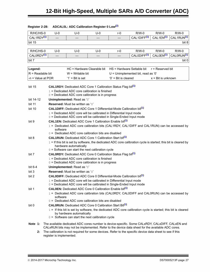
Register 2-28: ADCAL0L: ADC Calibration Register 0 Low(2)
R/HC/HS-0 U-0 U-0 U-0 r-0 R/W-0 R/W-0 R/W-0
CAL1RDY(1) — — — — CAL1DIFF(1) CAL1EN(1) CAL1RUN(1)
bit 15 bit 8
R/HC/HS-0 U-0 U-0 U-0 r-0 R/W-0 R/W-0 R/W-0
CAL0RDY(1) — — — — CAL0DIFF(1) CAL0EN(1) CAL0RUN(1)
bit 7 bit 0
Legend: HC = Hardware Clearable bit HS = Hardware Settable bit r = Reserved bit
R = Readable bit W = Writable bit U = Unimplemented bit, read as ‘0’
-n = Value at POR ‘1’ = Bit is set ‘0’ = Bit is cleared x = Bit is unknown
bit 15 CAL1RDY: Dedicated ADC Core 1 Calibration Status Flag bit(1)
1 = Dedicated ADC core calibration is finished0 = Dedicated ADC core calibration is in progress
bit 14-12 Unimplemented: Read as ‘0’
bit 11 Reserved: Must be written as ‘0’
bit 10 CAL1DIFF: Dedicated ADC Core 1 Differential-Mode Calibration bit(1)
1 = Dedicated ADC core will be calibrated in Differential Input mode0 = Dedicated ADC core will be calibrated in Single-Ended Input mode
bit 9 CAL1EN: Dedicated ADC Core 1 Calibration Enable bit(1)
1 = Dedicated ADC core calibration bits (CAL1RDY, CAL1DIFF and CAL1RUN) can be accessed bysoftware
0 = Dedicated ADC core calibration bits are disabled
bit 8 CAL1RUN: Dedicated ADC Core 1 Calibration Start bit(1)
1 = If this bit is set by software, the dedicated ADC core calibration cycle is started; this bit is cleared byhardware automatically
0 = Software can start the next calibration cycle
bit 7 CAL0RDY: Dedicated ADC Core 0 Calibration Status Flag bit(1)
1 = Dedicated ADC core calibration is finished0 = Dedicated ADC core calibration is in progress
bit 6-4 Unimplemented: Read as ‘0’
bit 3 Reserved: Must be written as ‘0’
bit 2 CAL0DIFF: Dedicated ADC Core 0 Differential-Mode Calibration bit(1)
1 = Dedicated ADC core will be calibrated in Differential Input mode0 = Dedicated ADC core will be calibrated in Single-Ended Input mode
bit 1 CAL0EN: Dedicated ADC Core 0 Calibration Enable bit(1)
1 = Dedicated ADC core calibration bits (CAL0RDY, CAL0DIFF and CAL0RUN) can be accessed bysoftware
0 = Dedicated ADC core calibration bits are disabled
bit 0 CAL0RUN: Dedicated ADC Core 0 Calibration Start Bit(1)
1 = If this bit is set by software, the dedicated ADC core calibration cycle is started; this bit is clearedby hardware automatically
0 = Software can start the next calibration cycle
Note 1: The available dedicated ADC cores number is device-specific. Some CALxRDY, CALxDIFF, CALxEN and CALxRUN bits may not be implemented. Refer to the device data sheet for the available ADC cores.
2: The calibration is not required for some devices. Refer to the specific device data sheet to see if this register is implemented.
2014-2017 Microchip Technology Inc. DS70005213F-page 27

dsPIC33/PIC24 Family Reference Manual
Register 2-29: ADCAL0H: ADC Calibration Register 0 High(2)
R/HC/HS-0 U-0 U-0 U-0 r-0 R/W-0 R/W-0 R/W-0
CAL3RDY(1) — — — — CAL3DIFF(1) CAL3EN(1) CAL3RUN(1)
bit 15 bit 8
R/HC/HS-0 U-0 U-0 U-0 r-0 R/W-0 R/W-0 R/W-0
CAL2RDY(1) — — — — CAL2DIFF(1) CAL2EN(1) CAL2RUN(1)
bit 7 bit 0
Legend: HC = Hardware Clearable bit HS = Hardware Settable bit r = Reserved bit
R = Readable bit W = Writable bit U = Unimplemented bit, read as ‘0’
-n = Value at POR ‘1’ = Bit is set ‘0’ = Bit is cleared x = Bit is unknown
bit 15 CAL3RDY: Dedicated ADC Core 3 Calibration Status Flag bit(1)
1 = Dedicated ADC core calibration is finished0 = Dedicated ADC core calibration is in progress
bit 14-12 Unimplemented: Read as ‘0’
bit 11 Reserved: Must be written as ‘0’
bit 10 CAL3DIFF: Dedicated ADC Core 3 Differential-Mode Calibration bit(1)
1 = Dedicated ADC core will be calibrated in Differential Input mode0 = Dedicated ADC core will be calibrated in Single-Ended Input mode
bit 9 CAL3EN: Dedicated ADC Core 3 Calibration Enable bit(1)
1 = Dedicated ADC core calibration bits (CAL3RDY, CAL3DIFF and CAL3RUN) can be accessed bysoftware.
0 = Dedicated ADC core calibration bits are disabled
bit 8 CAL3RUN: Dedicated ADC Core 3 Calibration Start bit(1)
1 = If this bit is set by software, the dedicated ADC core calibration cycle is started; this bit is cleared byhardware automatically
0 = Software can start the next calibration cycle
bit 7 CAL2RDY: Dedicated ADC Core 2 Calibration Status Flag bit(1)
1 = Dedicated ADC core calibration is finished0 = Dedicated ADC core calibration is in progress
bit 6-4 Unimplemented: Read as ‘0’
bit 3 Reserved: Must be written as ‘0’
bit 2 CAL2DIFF: Dedicated ADC Core 2 Differential-Mode Calibration bit(1)
1 = Dedicated ADC core will be calibrated in Differential Input mode0 = Dedicated ADC core will be calibrated in Single-Ended Input mode
bit 1 CAL2EN: Dedicated ADC Core 2 Calibration Enable bit(1)
1 = Dedicated ADC core calibration bits (CAL2RDY, CAL2DIFF and CAL2RUN) can be accessed bysoftware
0 = Dedicated ADC core calibration bits are disabled
bit 0 CAL2RUN: Dedicated ADC Core 2 Calibration Start bit(1)
1 = If this bit is set by software, the dedicated ADC core calibration cycle is started; this bit is cleared byhardware automatically
0 = Software can start the next calibration cycle
Note 1: The available dedicated ADC cores number is device-specific. Some CALxRDY, CALxDIFF, CALxEN and CALxRUN bits may not be implemented. Refer to the device data sheet for the available ADC cores.
2: The calibration is not required for some devices. Refer to the specific device data sheet to see if this register is implemented.
DS70005213F-page 28 2014-2017 Microchip Technology Inc.

12-Bit High-Speed, Multiple SARs A/D Converter (ADC)
Register 2-30: ADCAL1L: ADC Calibration Register 1 Low(2)
R/HC/HS-0 U-0 U-0 U-0 r-0 R/W-0 R/W-0 R/W-0
CAL5RDY(1) — — — — CAL5DIFF(1) CAL5EN(1) CAL5RUN(1)
bit 15 bit 8
R/HC/HS-0 U-0 U-0 U-0 r-0 R/W-0 R/W-0 R/W-0
CAL4RDY(1) — — — — CAL4DIFF(1) CAL4EN(1) CAL4RUN(1)
bit 7 bit 0
Legend: HC = Hardware Clearable bit HS = Hardware Settable bit r = Reserved bit
R = Readable bit W = Writable bit U = Unimplemented bit, read as ‘0’
-n = Value at POR ‘1’ = Bit is set ‘0’ = Bit is cleared x = Bit is unknown
bit 15 CAL5RDY: Dedicated ADC Core 5 Calibration Status Flag bit(1)
1 = Dedicated ADC core calibration is finished0 = Dedicated ADC core calibration is in progress
bit 14-12 Unimplemented: Read as ‘0’
bit 11 Reserved: Must be written as ‘0’
bit 10 CAL5DIFF: Dedicated ADC Core 5 Differential-Mode Calibration bit(1)
1 = Dedicated ADC core will be calibrated in differential input mode0 = Dedicated ADC core will be calibrated in single-ended input mode
bit 9 CAL5EN: Dedicated ADC Core 5 Calibration Enable bit(1)
1 = Dedicated ADC core calibration bits (CAL5RDY, CAL5DIFF and CAL5RUN) can be accessed bysoftware
0 = Dedicated ADC core calibration bits are disabled
bit 8 CAL5RUN: Dedicated ADC Core 5 Calibration Start bit(1)
1 = If this bit is set by software, the dedicated ADC core calibration cycle is started; this bit is cleared byhardware automatically
0 = Software can start the next calibration cycle
bit 7 CAL4RDY: Dedicated ADC Core 4 Calibration Status Flag bit(1)
1 = Dedicated ADC core calibration is finished0 = Dedicated ADC core calibration is in progress
bit 6-4 Unimplemented: Read as ‘0’
bit 3 Reserved: Must be written as ‘0’
bit 2 CAL4DIFF: Dedicated ADC Core 4 Differential-Mode Calibration bit(1)
1 = Dedicated ADC core will be calibrated in Differential Input mode0 = Dedicated ADC core will be calibrated in Single-Ended Input mode
bit 1 CAL4EN: Dedicated ADC Core 4 Calibration Enable bit(1)
1 = Dedicated ADC core calibration bits (CAL4RDY, CAL4DIFF and CAL4RUN) can be accessed bysoftware
0 = Dedicated ADC core calibration bits are disabled
bit 0 CAL4RUN: Dedicated ADC Core 4 Calibration Start bit(1)
1 = If this bit is set by software, the dedicated ADC core calibration cycle is started. This bit is cleared byhardware automatically
0 = Software can start the next calibration cycle
Note 1: The available dedicated ADC cores number is device-specific. Some CALxRDY, CALxDIFF, CALxEN and CALxRUN bits may not be implemented. Refer to the device data sheet for the available ADC cores.
2: The calibration is not required for some devices. Refer to the specific device data sheet to see if this register is implemented.
2014-2017 Microchip Technology Inc. DS70005213F-page 29

dsPIC33/PIC24 Family Reference Manual
Register 2-31: ADCAL1H: ADC Calibration Register 1 High(2)
R/HC/HS-0 U-0 U-0 U-0 r-0 R/W-0 R/W-0 R/W-0
CSHRRDY — — — — CSHRDIFF CSHREN CSHRRUN
bit 15 bit 8
R/HC/HS-0 U-0 U-0 U-0 r-0 R/W-0 R/W-0 R/W-0
CAL6RDY(1) — — — — CAL6DIFF(1) CAL6EN(1) CAL6RUN(1)
bit 7 bit 0
Legend: HC = Hardware Clearable bit HS = Hardware Settable bit r = Reserved bit
R = Readable bit W = Writable bit U = Unimplemented bit, read as ‘0’
-n = Value at POR ‘1’ = Bit is set ‘0’ = Bit is cleared x = Bit is unknown
bit 15 CSHRRDY: Shared ADC Core Calibration Status Flag bit
1 = Shared ADC core calibration is finished0 = Shared ADC core calibration is in progress
bit 14-12 Unimplemented: Read as ‘0’
bit 11 Reserved: Must be written as ‘0’
bit 10 CSHRDIFF: Shared ADC Core Differential-Mode Calibration bit
1 = Shared ADC core will be calibrated in Differential Input mode0 = Shared ADC core will be calibrated in Single-Ended Input mode
bit 9 CSHREN: Shared ADC Core Calibration Enable bit
1 = Shared ADC core calibration bits (CSHRRDY, CSHRDIFF and CSHRRUN) can be accessed bysoftware
0 = Shared ADC core calibration bits are disabled
bit 8 CSHRRUN: Shared ADC Core Calibration Start bit
1 = If this bit is set by software, the shared ADC core calibration cycle is started; this bit is cleared byhardware automatically
0 = Software can start the next calibration cycle
bit 7 CAL6RDY: Dedicated ADC Core 6 Calibration Status Flag bit(1)
1 = Dedicated ADC core calibration is finished0 = Dedicated ADC core calibration is in progress
bit 6-4 Unimplemented: Read as ‘0’
bit 3 Reserved: Must be written as ‘0’
bit 2 CAL6DIFF: Dedicated ADC Core 6 Differential-Mode Calibration bit(1)
1 = Dedicated ADC core will be calibrated in Differential Input mode0 = Dedicated ADC core will be calibrated in Single-Ended Input mode
bit 1 CAL6EN: Dedicated ADC Core 6 Calibration Enable bit(1)
1 = Dedicated ADC core calibration bits (CAL6RDY, CAL6DIFF and CAL6RUN) can be accessed bysoftware
0 = Dedicated ADC core calibration bits are disabled
bit 0 CAL6RUN: Dedicated ADC Core 6 Calibration Start bit(1)
1 = If this bit is set by software, the dedicated ADC core calibration cycle is started; this bit is cleared byhardware automatically
0 = Software can start the next calibration cycle
Note 1: The available dedicated ADC cores number is device-specific. Some CALxRDY, CALxDIFF, CALxEN and CALxRUN bits may not be implemented. Refer to the device data sheet for the available ADC cores.
2: The calibration is not required for some devices. Refer to the specific device data sheet to see if this register is implemented.
DS70005213F-page 30 2014-2017 Microchip Technology Inc.

12-Bit High-Speed, Multiple SARs A/D Converter (ADC)
Register 2-32: ADCMPnCON: ADC Digital Comparator n Control Register(1)
U-0 U-0 U-0 R/HC/HS-0 R/HC/HS-0 R/HC/HS-0 R/HC/HS-0 R/HC/HS-0
— — — CHNL4 CHNL3 CHNL2 CHNL1 CHNL0
bit 15 bit 8
R/W-0 R/W-0 R/HC/HS-0 R/W-0 R/W-0 R/W-0 R/W-0 R/W-0
CMPEN IE STAT BTWN HIHI HILO LOHI LOLO
bit 7 bit 0
Legend: HC = Hardware Clearable bit HS = Hardware Settable bit
R = Readable bit W = Writable bit U = Unimplemented bit, read as ‘0’
-n = Value at POR ‘1’ = Bit is set ‘0’ = Bit is cleared x = Bit is unknown
bit 15-13 Unimplemented: Read as ‘0’
bit 12-8 CHNL<4:0>: Input Channel Number bits
These bits identify the analog input that caused the comparator event.11111 = AN31•••00001 = AN100000 = AN0
bit 7 CMPEN: Digital Comparator Enable bit
1 = Comparator is enabled0 = Comparator is disabled and the STAT status bit is cleared
bit 6 IE: Comparator Interrupts Enable bit
1 = individual and common interrupts will be generated if the comparator detects a comparison event0 = Individual and common interrupts will not be generated for the comparator
bit 5 STAT: Comparator Event Status bit
This bit is cleared by hardware when the channel number is read from the CHNL<4:0> bits.1 = A comparison event has been detected since the last read of the CHNL<4:0> bits0 = A comparison event has not been detected since the last read of the CHNL<4:0> bits
bit 4 BTWN: Between Low/High Comparator Event bit
1 = Generates a comparator event when ADCMPnLO ≤ ADCBUFx < ADCMPnHI0 = Does not generate a digital comparator event when ADCMPnLO ≤ ADCBUFx < ADCMPnHI
bit 3 HIHI: High/High Comparator Event bit
1 = Generates a digital comparator event when ADCBUFx ≥ ADCMPnHI0 = Does not generate a digital comparator event when ADCBUFx ≥ ADCMPnHI
bit 2 HILO: High/Low Comparator Event bit
1 = Generates a digital comparator event when ADCBUFx < ADCMPnHI0 = Does not generate a digital comparator event when ADCBUFx < ADCMPnHI
bit 1 LOHI: Low/High Comparator Event bit
1 = Generates a digital comparator event when ADCBUFx ≥ ADCMPnLO0 = Does not generate a digital comparator event when ADCBUFx ≥ ADCMPnLO
bit 0 LOLO: Low/Low Comparator Event bit
1 = Generates a digital comparator event when ADCBUFx < ADCMPnLO0 = Does not generate a digital comparator event when ADCBUFx < ADCMPnLO
Note 1: The available digital comparators number is device-specific. Refer to the device data sheet for the available digital comparators.
2014-2017 Microchip Technology Inc. DS70005213F-page 31

dsPIC33/PIC24 Family Reference Manual
Register 2-33: ADCMPnENL: ADC Digital Comparator n Channel Enable Register Low(1)
R/W/0 R/W-0 R/W-0 R/W-0 R/W-0 R/W-0 R/W-0 R/W-0
CMPEN<15:8>(2)
bit 15 bit 8
R/W/0 R/W-0 R/W-0 R/W-0 R/W-0 R/W-0 R/W-0 R/W-0
CMPEN<7:0>(2)
bit 7 bit 0
Legend:
R = Readable bit W = Writable bit U = Unimplemented bit, read as ‘0’
-n = Value at POR ‘1’ = Bit is set ‘0’ = Bit is cleared x = Bit is unknown
bit 15-0 CMPEN<15:0>: Comparator Enable for Corresponding Input Channels bits(2)
1 = Conversion result for corresponding channel is used by the comparator0 = Conversion result for corresponding channel is not used by the comparator
Note 1: The available digital comparators number is device-specific. Refer to the device data sheet for the available digital comparators.
2: The available channels are device-specific. Some CMPENx bits may not be implemented. Refer to the device data sheet for the available channels.
Register 2-34: ADCMPnENH: ADC Digital Comparator n Channel Enable Register High(1)
R/W/0 R/W-0 R/W-0 R/W-0 R/W-0 R/W-0 R/W-0 R/W-0
CMPEN<31:24>(2)
bit 15 bit 8
R/W/0 R/W-0 R/W-0 R/W-0 R/W-0 R/W-0 R/W-0 R/W-0
CMPEN<23:16>(2)
bit 7 bit 0
Legend:
R = Readable bit W = Writable bit U = Unimplemented bit, read as ‘0’
-n = Value at POR ‘1’ = Bit is set ‘0’ = Bit is cleared x = Bit is unknown
bit 15-0 CMPEN<31:16>: Comparator Enable for Corresponding Input Channels bits(2)
1 = Conversion result for corresponding channel is used by the comparator0 = Conversion result for corresponding channel is not used by the comparator
Note 1: The available digital comparators number is device-specific. Refer to the device data sheet for the available digital comparators.
2: The available channels are device-specific. Some CMPENx bits may not be implemented. Refer to the device data sheet for the available channels.
DS70005213F-page 32 2014-2017 Microchip Technology Inc.

12-Bit High-Speed, Multiple SARs A/D Converter (ADC)
Register 2-35: ADFLnCON: ADC Digital Filter n Control Register(1)
R/W-0 R/W-0 R/W-0 R/W-0 R/W-0 R/W-0 R/W-0 R/HC/HS-0
FLEN MODE1 MODE0 OVRSAM2 OVRSAM1 OVRSAM0 IE RDY
bit 15 bit 8
U-0 U-0 U-0 R/W-0 R/W-0 R/W-0 R/W-0 R/W-0
— — — FLCHSEL4 FLCHSEL3 FLCHSEL2 FLCHSEL1 FLCHSEL0
bit 7 bit 0
Legend: HC = Hardware Clearable bit HS = Hardware Settable bit
R = Readable bit W = Writable bit U = Unimplemented bit, read as ‘0’
-n = Value at POR ‘1’ = Bit is set ‘0’ = Bit is cleared x = Bit is unknown
bit 15 FLEN: Filter Enable bit
1 = Filter is enabled0 = Filter is disabled and the RDY bit is cleared
bit 14-13 MODE<1:0>: Filter Mode bits
11 = Averaging mode10 = Reserved01 = Reserved00 = Oversampling mode
bit 12-10 OVRSAM<2:0>: Filter Averaging/Oversampling Ratio bits
If MODE<1:0> = 00:111 = 128x (16-bit result in the ADFLnDAT register)110 = 32x (15-bit result in the ADFLnDAT register)101 = 8x (14-bit result in the ADFLnDAT register)100 = 2x (13-bit result in the ADFLnDAT register)011 = 256x (16-bit result in the ADFLnDAT register)010 = 64x (15-bit result in the ADFLnDAT register)001 = 16x (14-bit result in the ADFLnDAT register)000 = 4x (13-bit result in the ADFLnDAT register)
If MODE<1:0> = 11 (12-bit result in the ADFLnDAT register):111 = 256x110 = 128x101 = 64x100 = 32x011 = 16x010 = 8x001 = 4x000 = 2x
bit 9 IE: Filter Interrupts Enable bit
1 = Individual and common interrupts will be generated when the filter result is ready0 = Individual and common interrupts will not be generated for the filter
bit 8 RDY: Oversampling Filter Data Ready Flag bit
This bit is cleared by hardware when the result is read from the ADFLnDAT register.1 = Data in the ADFLnDAT register is ready0 = The ADFLnDAT register has been read and new data in the ADFLnDAT register is not ready
bit 7-5 Unimplemented: Read as ‘0’
Note 1: The available oversampling filter number is device-specific. Refer to the device data sheet for the available oversampling filters.
2014-2017 Microchip Technology Inc. DS70005213F-page 33

dsPIC33/PIC24 Family Reference Manual
bit 4-0 FLCHSEL<4:0>: Oversampling Filter Input Channel Selection bits
11111 = AN31•••00001 = AN100000 = AN0
Register 2-35: ADFLnCON: ADC Digital Filter n Control Register(1) (Continued)
Note 1: The available oversampling filter number is device-specific. Refer to the device data sheet for the available oversampling filters.
DS70005213F-page 34 2014-2017 Microchip Technology Inc.

12-Bit High-Speed, Multiple SARs A/D Converter (ADC)
Register 2-36: ADCSSL: CVD Scan Select Register Low(1)
R/W/0 R/W-0 R/W-0 R/W-0 R/W-0 R/W-0 R/W-0 R/W-0
CSS<15:8>(2)
bit 15 bit 8
R/W/0 R/W-0 R/W-0 R/W-0 R/W-0 R/W-0 R/W-0 R/W-0
CSS<7:0>(2)
bit 7 bit 0
Legend:
R = Readable bit W = Writable bit U = Unimplemented bit, read as ‘0’
-n = Value at POR ‘1’ = Bit is set ‘0’ = Bit is cleared x = Bit is unknown
bit 15-0 CSS<15:0>: CVD Scan Enable for Corresponding Analog Inputs bits(2)
1 = The shared core analog input is included in the CVD scan0 = The shared core analog input is not scanned by CVD
Note 1: This register is not available if the CVD feature is not implemented. Refer to the device data sheet to see if CVD is available.
2: The available channels for the ADC shared core are device-specific. Some CSSx bits may not be implemented. Refer to the device data sheet for the available channels information.
Register 2-37: ADCSSH: CVD Scan Select Register High(1)
R/W/0 R/W-0 R/W-0 R/W-0 R/W-0 R/W-0 R/W-0 R/W-0
CSS<31:24>(2)
bit 15 bit 8
R/W/0 R/W-0 R/W-0 R/W-0 R/W-0 R/W-0 R/W-0 R/W-0
CSS<23:16>(2)
bit 7 bit 0
Legend:
R = Readable bit W = Writable bit U = Unimplemented bit, read as ‘0’
-n = Value at POR ‘1’ = Bit is set ‘0’ = Bit is cleared x = Bit is unknown
bit 15-0 CSS<31:16>: CVD Scan Enable for Corresponding Analog Inputs bits(2)
1 = The shared core analog input is included in the CVD scan0 = The shared core analog input is not scanned by CVD
Note 1: This register is not available if the CVD feature is not implemented. Refer to the device data sheet to see if CVD is available.
2: The available channels for the ADC shared core are device-specific. Some CSSx bits may not be implemented. Refer to the device data sheet for the available channels information.
2014-2017 Microchip Technology Inc. DS70005213F-page 35
dsPIC33/PIC24 Family Reference Manual
3.0 CONVERSION SEQUENCE
Analog-to-Digital conversion using the 12-Bit High-Speed, Multiple SARs ADC involves thefollowing three steps:
1. Sampling of the input signal.
2. Capture of the input signal (holding) and transfer to the converter.
3. Conversion of the analog signal to its digital representation.
Sampling of the input signal involves charging of the capacitor in the Sample-and-Hold (S/H) circuit.The sampling time must be adequate so that the capacitor charges to a value equal to the inputvoltage. At the appropriate time, the input is disconnected from the capacitor, and subsequently,the analog voltage is transferred to the converter. The converter then digitizes the analog signaland provides the result.
The converter requires a clock source and a reference voltage. The clock and reference voltagesources are selectable, as well as the clock prescaling.
4.0 ADC OPERATION
4.1 SAR ADC Cores
The number of dedicated SAR ADC cores available is device-specific. For more information,refer to the specific device data sheet.
The module may implement up to eight independent SAR ADC cores. It allows sampling signalssimultaneously from multiple analog inputs. The seven first SAR ADC cores (0 through 6) arereferred to as dedicated, since each has a single dedicated analog channel. Each channel isconnected and the ADC core samples (follows) the input signal voltage continuously. Thechannel for the dedicated ADC core is disconnected only when the conversion is started. Thededicated independent ADC cores allow an application to sample the associated analogchannels simultaneously and convert them in a single “snap shot”.
The last SAR ADC core is referred to as a shared core, as it is shared among the analog inputsthat are not associated with the dedicated ADC cores. For this core, the analog channel to besampled, and the sampling process, are controlled by the ADC module. When the conversion isnot in progress, all inputs are disconnected from the shared ADC core. By the trigger event, theADC connects the analog input defined in the trigger and samples the input signal during thespecified amount of time. After sampling is completed, the analog input is disconnected againand the conversion is performed.
DS70005213F-page 36 2014-2017 Microchip Technology Inc.

12-Bit High-Speed, Multiple SARs A/D Converter (ADC)
4.2 ADC Clock
The ADC module has different options for the clock source. The source can be selected usingthe CLKSEL<1:0> bits in the ADCON3H register. The selected source has a period, TSRC, andis divided by the ratio specified by the CLKDIV<5:0> bits in the ADCON3H register. After thisdivider, the result clock with the period, TCORESRC, goes to each SAR ADC core. Each ADC corehas its own clock divider that is configured with the ADCS<6:0> bits in the correspondingADCOREnH register for the dedicated core, and with the SHRADCS<6:0> bits in the ADCON2Lregister for the shared ADC core. After the divisions, each ADC core can have a different clockperiod, TADCORE. The maximum operation clock frequency for each SAR ADC core is limited by70 MHz. Thus, the clock settings must be selected to provide a Core Clock period, TADCORE,more than 14.3 nS. The module clock path diagram is shown in Figure 4-1.
Figure 4-1: ADC Module Clock Path Block Diagram
4.3 ADC Resolution
Each SAR ADC core resolution can be set individually using the RES<1:0> bits in theADCOREnH register for the corresponding dedicated core, and using the SHRRES<1:0> bits inthe ADCON1H register for the shared core.
Depending on the setting, the resolution of the ADC is either 12 bits, 10 bits, 8 bits or 6 bits. Bydefault after Reset, all cores are configured for 12-bit resolution.
TADCORE > 14.3 nS
InstructionClockFRC
FOSC
AUX Clock
Clock SourceSelection bits
(CLKSEL<1:0>in ADCON3H
Register)
Clock SourceDivider bits
(CLKDIV<5:0> inADCON3H Register)
ADC CoreInput ClockDivider bits
(ADCS<6:0>in ADCORE0H
Register)
ADC CoreInput ClockDivider bits
(ADCS<6:0>in ADCORE1H
Register)
TADCOREfor DedicatedADC Core 0
TADCOREfor DedicatedADC Core 1
TADCOREfor SharedADC Core
Shared ADCCore Input Clock
Divider bits(SHRADCS<6:0>
in ADCON2LRegister)
TCORESRCTSRC
2014-2017 Microchip Technology Inc. DS70005213F-page 37
dsPIC33/PIC24 Family Reference Manual
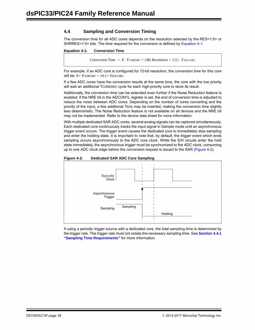
4.4 Sampling and Conversion Timing
The conversion time for all ADC cores depends on the resolution selected by the RES<1:0> orSHRRES<1:0> bits. The time required for the conversion is defined by Equation 4-1.
Equation 4-1: Conversion Time
For example, if an ADC core is configured for 12-bit resolution, the conversion time for this corewill be: 8 • TCORESRC + 14.5 • TADCORE.
If a few ADC cores have the conversion results at the same time, the core with the low prioritywill wait an additional TCORESRC cycle for each high-priority core to store its result.
Additionally, the conversion time can be extended even further if the Noise Reduction feature isenabled. If the NRE bit in the ADCON1L register is set, the end of conversion time is adjusted toreduce the noise between ADC cores. Depending on the number of cores converting and thepriority of the input, a few additional TADs may be inserted, making the conversion time slightlyless deterministic. The Noise Reduction feature is not available on all devices and the NRE bitmay not be implemented. Refer to the device data sheet for more information.
With multiple dedicated SAR ADC cores, several analog signals can be captured simultaneously.Each dedicated core continuously tracks the input signal in Sample mode until an asynchronoustrigger event occurs. The trigger event causes the dedicated core to immediately stop samplingand enter the holding state. It is important to note that, by default, the trigger event which endssampling occurs asynchronously to the ADC core clock. While the S/H circuits enter the holdstate immediately, the asynchronous trigger must be synchronized to the ADC clock, consumingup to one ADC clock edge before the conversion request is issued to the SAR (Figure 4-2).
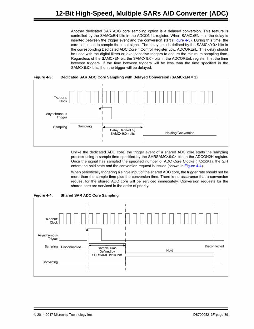
Figure 4-2: Dedicated SAR ADC Core Sampling
If using a periodic trigger source with a dedicated core, the total sampling time is determined bythe trigger rate. The trigger rate must not violate the necessary sampling time. See Section 4.4.1“Sampling Time Requirements” for more information.
Conversion Time 8 TCORESRC Bit Resolution 2.5+ TADCORE+=
TADCOREClock
AsynchronousTrigger
Sampling Sampling
Holding
DS70005213F-page 38 2014-2017 Microchip Technology Inc.
12-Bit High-Speed, Multiple SARs A/D Converter (ADC)
Another dedicated SAR ADC core sampling option is a delayed conversion. This feature iscontrolled by the SAMCxEN bits in the ADCON4L register. When SAMCxEN = 1, the delay isinserted between the trigger event and the conversion start (Figure 4-3). During this time, thecore continues to sample the input signal. The delay time is defined by the SAMC<9:0> bits inthe corresponding Dedicated ADC Core n Control Register Low, ADCOREnL. This delay shouldbe used with the digital filters or level-sensitive triggers to ensure the minimum sampling time.Regardless of the SAMCxEN bit, the SAMC<9:0> bits in the ADCOREnL register limit the timebetween triggers. If the time between triggers will be less than the time specified in theSAMC<9:0> bits, then the trigger will be delayed.
Figure 4-3: Dedicated SAR ADC Core Sampling with Delayed Conversion (SAMCxEN = 1)
Unlike the dedicated ADC core, the trigger event of a shared ADC core starts the samplingprocess using a sample time specified by the SHRSAMC<9:0> bits in the ADCON2H register.Once the signal has sampled the specified number of ADC Core Clocks (TADCORE), the S/Henters the hold state and the conversion request is issued (shown in Figure 4-4).
When periodically triggering a single input of the shared ADC core, the trigger rate should not bemore than the sample time plus the conversion time. There is no assurance that a conversionrequest for the shared ADC core will be serviced immediately. Conversion requests for theshared core are serviced in the order of priority.
Figure 4-4: Shared SAR ADC Core Sampling
TADCOREClock
AsynchronousTrigger
Sampling SamplingDelay Defined bySAMC<9:0> bits Holding/Conversion
TADCOREClock
AsynchronousTrigger
Sampling Disconnected Sample TimeDefined by Hold
Converting
SHRSAMC<9:0> bits
Disconnected
2014-2017 Microchip Technology Inc. DS70005213F-page 39

dsPIC33/PIC24 Family Reference Manual
4.4.1 SAMPLING TIME REQUIREMENTS
The analog input model of the 12-Bit High-Speed, Multiple SARs ADC is illustrated in Figure 4-5.The total acquisition time for the Analog-to-Digital conversion is a function of the Holding Capacitor(CHOLD) charge time.
For the ADC module to meet its specified accuracy, the Holding Capacitor (CHOLD) must beallowed to fully charge to the voltage level on the analog input pin. The analog output SourceImpedance (RS), the Interconnect Impedance (RIC) and the internal Sampling Switch Impedance(RSS) combine to directly affect the time required to charge the CHOLD. The combined impedanceof the analog sources must therefore, be small enough to fully charge the Holding Capacitorwithin the selected sample time. The internal Holding Capacitor will be in the discharged stateprior to each sample operation.
Figure 4-5: 12-Bit ADC Analog Input Model
4.5 Voltage Reference
The voltage reference options vary by device. Refer to the device data sheet for the specificoptions.
The ADC Reference Voltage Selection bits, REFSEL<2:0> in the ADCON3L register, select thevoltage reference for all SAR ADC cores. Also, the ADC module depends on the internal band gapcircuit voltage. When the voltage reference and the band gap are ready for operation, theREFRDY bit in ADCON2H is set. The voltage reference source cannot be changed when themodule is enabled (ADON (ADCON1L<15>) = 1). If the ADC reference or AVDD power waschanged or interrupted, the REFERR bit in the ADCON2H register is set. After a voltagereference Fault event is detected, the ADC module must be recalibrated. The voltage referenceready and voltage reference Fault events, indicated by the REFRDY and REFERR bits, cangenerate common interrupts if the corresponding REFCIE and REFERCIE bits are set in theADCON2L register. To avoid false Fault interrupts, the REFERCIE bit must be set only after themodule is enabled (ADON = 1).
CPIN(1)
Rs ANxVT = 0.6V
VT = 0.6V ILEAKAGE
RIC = 300 SamplingSwitch
RSS
CHOLD = 5 pF
VSS
VDD
±500 nA
Note 1: The CPIN value depends on the device package and is not tested. The effect of the CPIN is negligible if Rs 5 k.
RSS = 44
Legend:
CPIN = Input Capacitance VT = Threshold Voltage
RSS = Sampling Switch Resistance RIC = Interconnect Resistance
RS = Source Resistance CHOLD = Sample/Hold Capacitance
ILEAKAGE = Leakage Current at the Pin due to Various Junctions
VA
DS70005213F-page 40 2014-2017 Microchip Technology Inc.
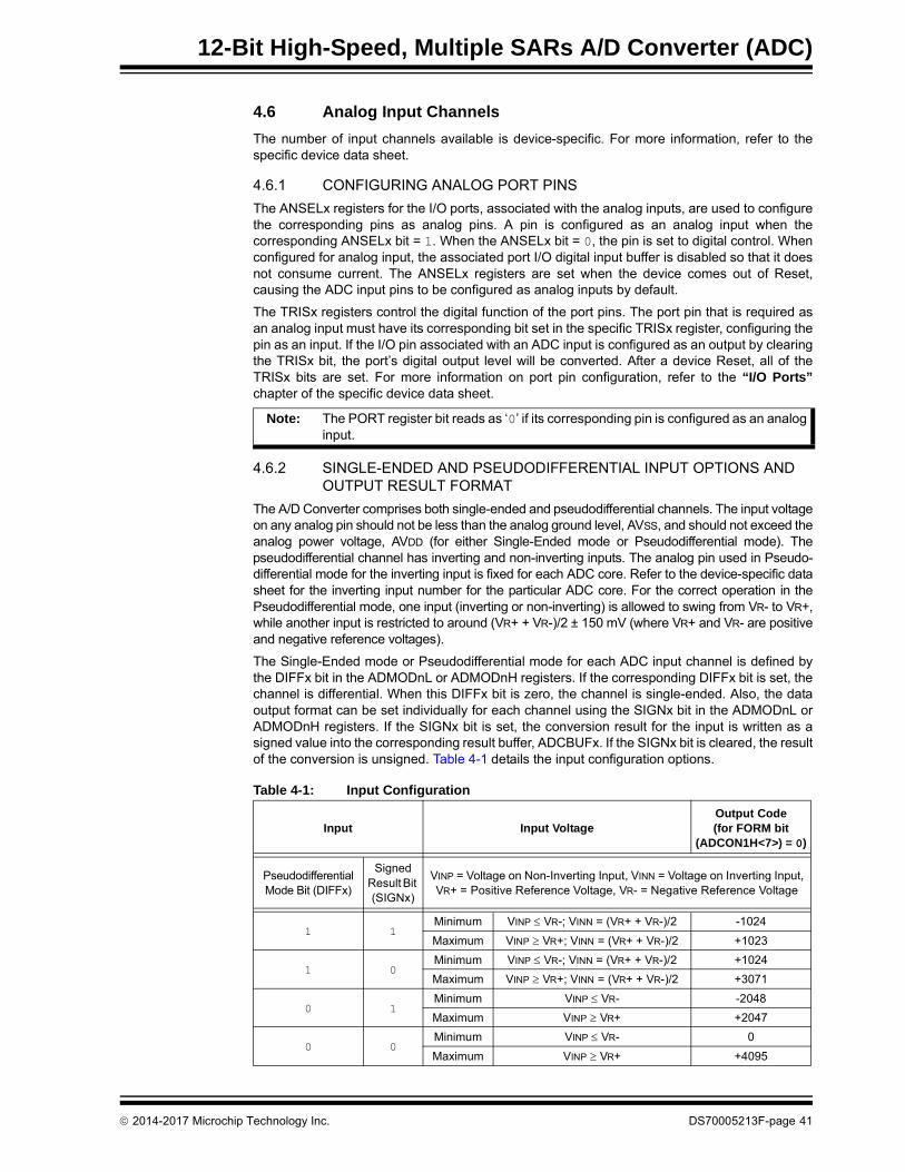
12-Bit High-Speed, Multiple SARs A/D Converter (ADC)
4.6 Analog Input Channels
The number of input channels available is device-specific. For more information, refer to thespecific device data sheet.
4.6.1 CONFIGURING ANALOG PORT PINS
The ANSELx registers for the I/O ports, associated with the analog inputs, are used to configurethe corresponding pins as analog pins. A pin is configured as an analog input when thecorresponding ANSELx bit = 1. When the ANSELx bit = 0, the pin is set to digital control. Whenconfigured for analog input, the associated port I/O digital input buffer is disabled so that it doesnot consume current. The ANSELx registers are set when the device comes out of Reset,causing the ADC input pins to be configured as analog inputs by default.
The TRISx registers control the digital function of the port pins. The port pin that is required asan analog input must have its corresponding bit set in the specific TRISx register, configuring thepin as an input. If the I/O pin associated with an ADC input is configured as an output by clearingthe TRISx bit, the port’s digital output level will be converted. After a device Reset, all of theTRISx bits are set. For more information on port pin configuration, refer to the “I/O Ports”chapter of the specific device data sheet.
4.6.2 SINGLE-ENDED AND PSEUDODIFFERENTIAL INPUT OPTIONS AND OUTPUT RESULT FORMAT
The A/D Converter comprises both single-ended and pseudodifferential channels. The input voltageon any analog pin should not be less than the analog ground level, AVSS, and should not exceed theanalog power voltage, AVDD (for either Single-Ended mode or Pseudodifferential mode). Thepseudodifferential channel has inverting and non-inverting inputs. The analog pin used in Pseudo-differential mode for the inverting input is fixed for each ADC core. Refer to the device-specific datasheet for the inverting input number for the particular ADC core. For the correct operation in thePseudodifferential mode, one input (inverting or non-inverting) is allowed to swing from VR- to VR+,while another input is restricted to around (VR+ + VR-)/2 ± 150 mV (where VR+ and VR- are positiveand negative reference voltages).
The Single-Ended mode or Pseudodifferential mode for each ADC input channel is defined bythe DIFFx bit in the ADMODnL or ADMODnH registers. If the corresponding DIFFx bit is set, thechannel is differential. When this DIFFx bit is zero, the channel is single-ended. Also, the dataoutput format can be set individually for each channel using the SIGNx bit in the ADMODnL orADMODnH registers. If the SIGNx bit is set, the conversion result for the input is written as asigned value into the corresponding result buffer, ADCBUFx. If the SIGNx bit is cleared, the resultof the conversion is unsigned. Table 4-1 details the input configuration options.
Note: The PORT register bit reads as ‘0’ if its corresponding pin is configured as an analoginput.
Table 4-1: Input Configuration
Input Input VoltageOutput Code (for FORM bit
(ADCON1H<7>) = 0)
Pseudodifferential Mode Bit (DIFFx)
Signed Result Bit (SIGNx)
VINP = Voltage on Non-Inverting Input, VINN = Voltage on Inverting Input, VR+ = Positive Reference Voltage, VR- = Negative Reference Voltage
1 1Minimum VINP VR-; VINN = (VR+ + VR-)/2 -1024
Maximum VINP VR+; VINN = (VR+ + VR-)/2 +1023
1 0Minimum VINP VR-; VINN = (VR+ + VR-)/2 +1024
Maximum VINP VR+; VINN = (VR+ + VR-)/2 +3071
0 1Minimum VINP VR- -2048
Maximum VINP VR+ +2047
0 0Minimum VINP VR- 0
Maximum VINP VR+ +4095
2014-2017 Microchip Technology Inc. DS70005213F-page 41

dsPIC33/PIC24 Family Reference Manual
4.6.3 SELECTING ANALOG INPUT FOR DEDICATED ADC CORE
To provide greater flexibility to the dedicated ADC cores, several inputs are provided for each.These may include the analog pins and the outputs of other analog modules, such as amplifiers.The input options are chosen using the CxCHS<1:0> bits in the ADCON4H register.
The input options are device-specific. For more information, refer to the device data sheet. TheCxCHS<1:0> bits physically connect different analog inputs to the dedicated ADC core, but theydo not change the trigger source. The dedicated ADC core accepts only triggers from thechannel corresponding to the CxCHS<1:0> = 00 option, regardless of the value written into theCxCHS<1:0> bits.
4.6.4 INPUT PRIORITY
To resolve simultaneous requests for input conversions between different channels, the sharedADC core uses a natural order priority scheme. The priority scheme is fixed and is defined by theinput channel number, with the channel with lowest number receiving the highest priority. In otherwords, input conversions occur in ascending order of the analog channel number, with the lowestchannel number being converted first.
4.7 Enabling the ADC
The ADC module has several levels of activation (see Figure 4-6).
Figure 4-6: ADC Module Activation.
Note: The CxCHS<1:0> bits do not change the trigger source channel for the dedicatedcore. The trigger source is defined by the default channel assigned to the core.Usually, for dedicated Core 0, the trigger is always selected by the TRGSRC0<4:0>bits; for dedicated Core 1, it is always selected by the TRGSCR1<4:0> bits and soon. Refer to the device data sheet for the details of the trigger options. Also,regardless of the CxCHS<1:0> bits value, the conversion result for dedicated coresis stored in ADCBUF0 for Core 0, in ADCBUF1 for Core 1 and so on.
Set ADC CoresInitialization TimeMore than 10 S
(WARMTIME<3:0> bitsin ADCON5H Register)
ADC Module Enable(ADON bit in
ADCON1L Register)
Dedicated ADC Core 0ANALOG Circuits PowerControl (C0PWR bit inADCON5L Register)
Dedicated ADC Core 0DIGITAL Circuits Enable
(C0EN bit inADCON3H Register)
Dedicated ADC Core 1ANALOG Circuits PowerControl (C1PWR bit inADCON5L Register)
Dedicated ADC Core 1DIGITAL Circuits Enable
(C1EN bit inADCON3H Register)
Shared ADC CoreANALOG Circuits PowerControl (SHRPWR bit in
ADCON5L Register)
Shared ADC CoreDIGITAL Circuits Enable
(SHREN bit inADCON3H Register)
C0RDY bit inADCON5L
Indicates whenthe Core is Ready
C1RDY bit inADCON5L
Indicates whenthe Core is Ready
SHRRDY bit inADCON5L
Indicates whenthe Core is Ready
DS70005213F-page 42 2014-2017 Microchip Technology Inc.
12-Bit High-Speed, Multiple SARs A/D Converter (ADC)
The ADON bit in the ADCON1L register enables the ADC module as a whole. Then, each SARADC core should be switched on individually. The CxPWR and SHRPWR bits in the ADCON5Lregister control the analog circuits of the dedicated and shared ADC cores accordingly. When theCxPWR or SHRPWR bits are set, the power-on delay is inserted to stabilize the analog circuits.The delay value is defined by the WARMTIME<3:0> bits in the ADCON5H register. After the delay,the corresponding CxRDY or SHRRDY bit is set in the ADCON5L register to indicate that the ADCcore is ready for operation. At this point, the ADC cores do not receive the triggers. To enable theADC core digital circuit, the CxEN or SHREN bit must be set in the ADCON3H register for thededicated and shared ADC cores accordingly. When the CxEN or SHREN bits are set, thecorresponding SAR ADC core is fully operational. The SAR ADC cores require 10 µS initializationtime. The WARMTIME<3:0> bits must be configured to provide enough time for the initialization.
To enable the ADC module, the following steps should be performed:
1. Set the WARMTIME<3:0> bits in the ADCON5H register to provide at least 10 µS for theADC cores initialization.
2. Set the ADON bit in the ADCON1L register.
3. Set the CxPWR and/or SHRPWR bits in the ADCON5L register for the selected ADC cores.
4. Poll the CxRDY and/or SHRRDY bits in the ADCON5L register for the selected ADC coresuntil they are set.
5. Set the CxEN and/or SHREN bits in the ADCON3H register for the selected ADC cores.
The analog circuit ready events, indicated by the CxRDY and SHRRDY bits, can be used togenerate the common ADC interrupt. To do this, the corresponding CxCIE and/or SHRCIE bitsmust be set in the ADCON5H register.
4.8 Calibration
On some devices, whenever the module is enabled (refer to “Section 4.7 “Enabling the ADC”),the calibration of all SAR ADC cores must be performed. Refer to the specific device data sheetto see if the calibration is required and the Calibration registers, ADCALnL and ADCALnH, areimplemented. The ADCALnL and ADCALnH registers control the calibration process for allcores. Two calibration procedures must be done for each core. One procedure is used for Single-Ended Input mode when the CALxDIFF bits for the dedicated cores, and/or the CSHRDIFF bitfor the shared core, are cleared. The second procedure is used for the Differential-mode whenthe CALxDIFF and/or CSHRDIFF bits are set. The differential calibration can be skipped if onlySingle-Ended mode is used for the core. Also, the single-ended calibration is not required if thecore uses differential inputs only. To enter into the Calibration mode, the CALxEN bits and/orCSHREN bit (for dedicated cores and shared core accordingly) should be set. Then, theCALxRUN and/or CSHRRUN bits should be set to execute the calibration. These bits are clearedby hardware to allow the next calibration cycle. Also, when the CALxRUN and/or CSHRRUN bitsare set, the corresponding CALxRDY and/or CSHRRDY bits are cleared. The application shouldpoll the CALxRDY and CSHRRDY bits to detect the end of the calibration process. Aftercalibration, the CALxEN and/or CSHREN bits must be cleared in order to resume normaloperation on all SAR ADC cores.
To perform the SAR ADC cores’ calibration, the following steps should be done:
1. Set the CALxEN and/or CSHREN bits.
2. Clear the CALxDIFF and/or CSHRDIFF bits.
3. Set the CALxRUN and/or CSHRRUN bits.
4. Poll the CALxRDY and/or CSHRRDY bits until they are set.
5. Set the CALxDIFF and/or CSHRDIFF bits.
6. Set the CALxRUN and/or CSHRRUN bits.
7. Poll the CALxRDY and CSHRRDY bits until they are set.
8. Clear the CALxEN and/or CSHREN bits.
After the ADC module is enabled, the recalibration is required if the following ADC options arechanged:
• Voltage Reference (REFSEL<2:0> bits)• Clock (CLKSEL<1:0>, CLKDIV<5:0>, SHRADCS<6:0> and ADCS<6:0> bits)
2014-2017 Microchip Technology Inc. DS70005213F-page 43
dsPIC33/PIC24 Family Reference Manual
4.9 Triggering
There are four methods to initiate a conversion request:
• Individual Input Triggers
• Common Software Trigger
• Common Level-Sensitive Software Trigger
• Individual Input Software Trigger (one-shot trigger)
4.9.1 INDIVIDUAL INPUT TRIGGER
The application can independently specify an individual conversion trigger source for eachanalog input using the TRGSRCn<4:0> bits in the ADTRIGnL or ADTRIGnH register. Typicaltrigger sources may include general purpose timers, output compare modules, PWM generators,comparators, external pins, common software triggers and the common level-sensitive softwaretrigger. Each trigger source, selected by the TRGSRCn<4:0> bits, can be set as edge-sensitiveor level-sensitive using the LVLENx bit in the ADLVLTRGL or ADLVLTRGH register for thecorresponding channel. If the LVLENx bit is set, the ADC core will be triggered continuously aslong as the trigger signal is asserted. If the LVLENx bit is cleared, the ADC core will be triggeredjust once for the transition of the trigger signal. When the level-sensitive triggering is used for thededicated SAR ADC core, the corresponding SAMCxEN bit in the ADCON4L register should beset to give enough sampling time between conversions. The sampling time is defined by thecorresponding SAMC<9:0> bits in the ADCOREnL register.
4.9.2 CHANNEL SCAN
If it is necessary to scan several analog channels, this can be done by selecting the same triggersource for each channel using the TRGSRCn<4:0> bits in the ADTRIGnL or ADTRIGnH register.
4.9.3 COMMON SOFTWARE TRIGGER
The conversion of any analog input can be triggered by the Software Common Trigger bit,SWCTRG (ADCON3L<6>). This option is selected when the corresponding channel bits,TRGSRCn<4:0>, are set to ‘00001’ in the ADTRIGnL or ADTRIGnH register. The associatedanalog inputs will be triggered when the SWCTRG bit is set by the software. This bit isautomatically cleared by hardware, allowing the software to trigger another conversion if needed.
4.9.4 COMMON LEVEL-SENSITIVE SOFTWARE TRIGGER
The conversion of any analog input can be triggered by the Software Level-Sensitive CommonTrigger bit, SWLCTRG (ADCON3L<7>). To select this option, the TRGSRCn<4:0> bits must beset to ‘00010’ in the ADTRIGnL or ADTRIGnH register for the corresponding input channel. TheLVLENx bit must be set in the ADLVLTRGL or ADLVLTRGH register as well. When theSWLCTRG bit is set, the associated analog input will be triggered continuously until theSWLCTRG bit is cleared by the software. When the level-sensitive triggering is used for thededicated SAR ADC core, the corresponding SAMCxEN bit in the ADCON4L register should beset to give enough sampling time between the conversions. The sampling time is defined by thecorresponding SAMC<9:0> bits in the ADCOREnL register.
DS70005213F-page 44 2014-2017 Microchip Technology Inc.
12-Bit High-Speed, Multiple SARs A/D Converter (ADC)
4.9.5 INDIVIDUAL CHANNEL SOFTWARE TRIGGER
The application can explicitly request a single conversion of any selected analog input, at anytime during program execution, without changing the trigger source configuration of the ADC.The input to be converted should be specified by the CNVCHSEL<5:0> bits in the ADCON3Lregister. The CNVRTCH bit in the ADCON3L register is used to trigger the conversion. This bitis automatically cleared by hardware, allowing the application to trigger another conversion ifneeded.
4.9.6 TRIGGER SUSPENSION
The ADC module has a special SUSPEND bit in the ADCON3L register to suspend all triggersfor all ADC cores. When the SUSPEND bit is set, all future triggers for all SAR ADC cores will bedisabled. However, this bit does not cancel the ‘delayed by priority’ triggers and the triggers thatare currently in progress. After the triggers are suspended, the software should poll theSUSPRDY bit in the ADCON3L register to make sure that all pending triggers have beenserviced. When the SUSPEND and SUSPRDY bits are set, there are no triggers for all ADCcores. The SUSPRDY bit event can generate the common ADC interrupt if the SUSPCIE bit isset in the ADCON3L register.
2014-2017 Microchip Technology Inc. DS70005213F-page 45

dsPIC33/PIC24 Family Reference Manual
4.10 Conversion Result
The module contains the data output registers for each analog input to store the A/D results,called the ADCBUFx (where ‘x’ is the number of the analog channel). The buffers are read-only.When data is written into a data register, the associated ANxRDY bit in the ADSTATL orADSTATH register is set. When an ANxRDY bit is set, an interrupt request is generated. Whena specific data register is read, the associated ANxRDY bit is immediately cleared. If a bufferlocation has not been read by the software, and the ADC needs to overwrite that location with anew conversion result, the previous data is lost.
4.10.1 FORMAT OF THE ADC RESULT
Writes of data from the A/D Converter into the ADC Result registers pass through the data formatter.The resulting data is formatted into a 16-bit word.
The data in the ADC Result register can be read in any of the four supported data formats. Theuser can select from unsigned integer, signed integer, unsigned fractional or signed fractionalformat. Integer data is right justified and fractional data is left justified.
• The integer/fractional data format selection is specified globally for all ADC inputs using the FORM bit in the ADCON1H register.
• The signed/unsigned data format selection can be independently specified for each individ-ual input channel using the DIFFx and SIGNx bits in the ADMODnL or ADMODnH register, as described in Section 4.6.2 “Single-Ended and Pseudodifferential Input Options and Output Result Format”.
• Output data format depends on the ADC core resolution, specified by the RES<1:0> bits in the ADCOREnH register for the dedicated core and by the SHRRES<1:0> bits in the ADCON1H register for the shared core.
Figure 4-7, Figure 4-8, Figure 4-9 and Figure 4-10 illustrate how a result is formatted.
Figure 4-7: ADC Output Data Formats (12-Bit Resolution)
Analog-to-Digital Conversion Result
d11 d10 d09 d08 d07 d06 d05 d04 d03 d02 d01 d00
Unsigned Integer (SIGNx = 0, FORM = 0)
0 0 0 0 d11 d10 d09 d08 d07 d06 d05 d04 d03 d02 d01 d00
Signed Integer (SIGNx = 1, FORM = 0)
S S S S S d10 d09 d08 d07 d06 d05 d04 d03 d02 d01 d00
Fractional (SIGNx = 0, FORM = 1)
d11 d10 d09 d08 d07 d06 d05 d04 d03 d02 d01 d00 0 0 0 0
Signed Fractional (SIGNx = 1, FORM = 1)
S d10 d09 d08 d07 d06 d05 d04 d03 d02 d01 d00 0 0 0 0
DS70005213F-page 46 2014-2017 Microchip Technology Inc.
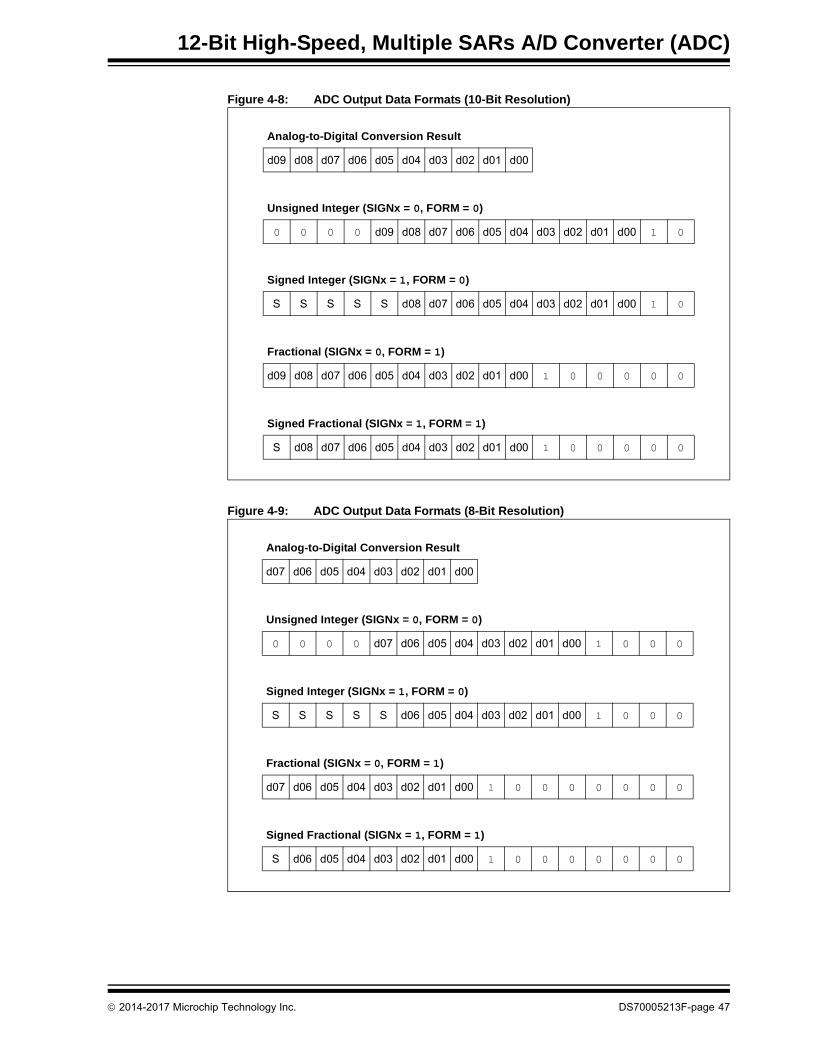
12-Bit High-Speed, Multiple SARs A/D Converter (ADC)
Figure 4-8: ADC Output Data Formats (10-Bit Resolution)
Figure 4-9: ADC Output Data Formats (8-Bit Resolution)
Analog-to-Digital Conversion Result
d09 d08 d07 d06 d05 d04 d03 d02 d01 d00
Unsigned Integer (SIGNx = 0, FORM = 0)
0 0 0 0 d09 d08 d07 d06 d05 d04 d03 d02 d01 d00 1 0
Signed Integer (SIGNx = 1, FORM = 0)
S S S S S d08 d07 d06 d05 d04 d03 d02 d01 d00 1 0
Fractional (SIGNx = 0, FORM = 1)
d09 d08 d07 d06 d05 d04 d03 d02 d01 d00 1 0 0 0 0 0
Signed Fractional (SIGNx = 1, FORM = 1)
S d08 d07 d06 d05 d04 d03 d02 d01 d00 1 0 0 0 0 0
Analog-to-Digital Conversion Result
d07 d06 d05 d04 d03 d02 d01 d00
Unsigned Integer (SIGNx = 0, FORM = 0)
0 0 0 0 d07 d06 d05 d04 d03 d02 d01 d00 1 0 0 0
Signed Integer (SIGNx = 1, FORM = 0)
S S S S S d06 d05 d04 d03 d02 d01 d00 1 0 0 0
Fractional (SIGNx = 0, FORM = 1)
d07 d06 d05 d04 d03 d02 d01 d00 1 0 0 0 0 0 0 0
Signed Fractional (SIGNx = 1, FORM = 1)
S d06 d05 d04 d03 d02 d01 d00 1 0 0 0 0 0 0 0
2014-2017 Microchip Technology Inc. DS70005213F-page 47

dsPIC33/PIC24 Family Reference Manual
Figure 4-10: ADC Output Data Formats (6-Bit Resolution)
Analog-to-Digital Conversion Result
d05 d04 d03 d02 d01 d00
Unsigned Integer (SIGNx = 0, FORM = 0)
0 0 0 0 d05 d04 d03 d02 d01 d00 1 0 0 0 0 0
Signed Integer (SIGNx = 1, FORM = 0)
S S S S S d04 d03 d02 d01 d00 1 0 0 0 0 0
Fractional (SIGNx = 0, FORM = 1)
d05 d04 d03 d02 d01 d00 1 0 0 0 0 0 0 0 0 0
Signed Fractional (SIGNx = 1, FORM = 1)
S d04 d03 d02 d01 d00 1 0 0 0 0 0 0 0 0 0
DS70005213F-page 48 2014-2017 Microchip Technology Inc.
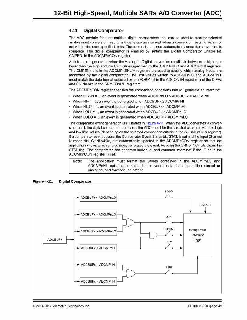
12-Bit High-Speed, Multiple SARs A/D Converter (ADC)
4.11 Digital Comparator
The ADC module features multiple digital comparators that can be used to monitor selectedanalog input conversion results and generate an interrupt when a conversion result is within, ornot within, the user-specified limits. The comparison occurs automatically once the conversion iscomplete. The digital comparator is enabled by setting the Digital Comparator Enable bit,CMPEN, in the ADCMPnCON register.
An interrupt is generated when the Analog-to-Digital conversion result is in between or higher, orlower than the high and low limit values specified by the ADCMPnLO and ADCMPnHI registers.The CMPENx bits in the ADCMPnENL/H registers are used to specify which analog inputs aremonitored by the digital comparator. The limit values written to ADCMPnLO and ADCMPnHImust match the data format selected by the FORM bit in the ADCON1H register, and the DIFFxand SIGNx bits in the ADMODnL/H registers.
The ADCMPnCON register specifies the comparison conditions that will generate an interrupt:
• When BTWN = 1, an event is generated when ADCMPnLO ≤ ADCBUFx < ADCMPnHI
• When HIHI = 1, an event is generated when ADCBUFx ADCMPnHI
• When HILO = 1, an event is generated when ADCBUFx < ADCMPnHI
• When LOHI = 1, an event is generated when ADCBUFx ADCMPnLO
• When LOLO = 1, an event is generated when ADCBUFx < ADCMPnLO
The comparator event generation is illustrated in Figure 4-11. When the ADC generates a conver-sion result, the digital comparator compares the ADC result for the selected channels with the highand low limit values (depending on the selected comparison criteria in the ADCMPnCON register).If a comparator event occurs, the Comparator Event Status bit, STAT, is set and the Input ChannelNumber bits, CHNL<4:0>, are automatically updated in the ADCMPnCON register so that theapplication knows which analog input generated the event. Reading the CHNL<4:0> bits clears theSTAT flag. The comparator can generate individual and common interrupts if the IE bit in theADCMPnCON register is set.
Figure 4-11: Digital Comparator
Note: The application must format the values contained in the ADCMPnLO andADCMPnHI registers to match the converted data format as either signed orunsigned, and fractional or integer.
ADCBUFx < ADCMPnLO
ADCBUFx = ADCMPnLO
ADCBUFx > ADCMPnLO
ADCBUFx < ADCMPnHI
ADCBUFx = ADCMPnHI
ADCBUFx > ADCMPnHI
LOLO
LOHI
HILO
HIHI
BTWN
CMPEN
ADCBUFx
Comparator
Interrupt
Logic
2014-2017 Microchip Technology Inc. DS70005213F-page 49

dsPIC33/PIC24 Family Reference Manual
4.12 Oversampling Digital Filter
The ADC module may support multiple oversampling digital filters. The filter consists of an accumu-lator and a decimator (down-sampler), which function together as a low-pass filter. By sampling ananalog input at a higher than required sample rate, and then processing the data through thefilter, the effective resolution of the ADC module can be increased at the expense of decreasedconversion throughput. For example, using 4x oversampling yields one extra bit of resolution,16x oversampling yields two extra bits of resolution, 64x oversampling provides three extra bitsof resolution and 256x oversampling provides four extra bits of resolution.
To perform a conversion using the oversampling digital filter:
1. Select the oversampling ratio with the OVRSAM<2:0> bits in the ADFLnCON register.
2. Set the sample time for subsequent conversions:
• For dedicated ADC core inputs, enable a delay between the trigger and the conversionstart by setting the corresponding SAMCxEN bit in the ADCON4L register, and selectthe sample time of the recurring conversions using the SAMC<9:0> bits in theADCOREnL register
• For shared ADC core inputs, select the sample time using the SHRSAMC<9:0> bits inthe ADCON2H register
3. Select the specific analog input to be oversampled by configuring the FLCHSEL<4:0> bitsin the ADFLnCON register.
4. Select the Averaging or Oversampling mode using the MODE<1:0> bits in the ADFLnCONregister.
5. Enable the oversampling filter by setting the FLEN bit.
Once the oversampling digital filter is configured, it waits for an input channel trigger to initiate theoversampling process. The trigger causes the accumulator to be cleared and initiates the firstconversion. After this initial trigger from the input channel, all of the next triggers are generatedby the filter itself automatically. Once each conversion request has been processed, sampling isinitiated based on the values of the SAMC<9:0> or SHRSAMC<9:0> bits for dedicated, or sharedADC core, respectively. This process continues until the required number of samples (4, 8, 16,32, 64, 128 or 256) has been converted. When the converted samples have been summed, theoutput is transferred to the ADFLnDAT register and the RDY bit in the ADFLnCON register is set.Reading the ADFLnDAT register clears the RDY flag. The filter will generate individual and com-mon interrupts if the IE bit in the ADFLnCON register is set. The filter does not support thefractional data format; if the filter is used, the FORM bit in the ADCON1H register must be ‘0’.
DS70005213F-page 50 2014-2017 Microchip Technology Inc.

12-Bit High-Speed, Multiple SARs A/D Converter (ADC)
Figure 4-12 illustrates 4x oversampling on an input for the dedicated ADC core. Prior to the trigger,the ADC core is tracking the input signal. The trigger starts the oversampling process. When thesampling delay defined by the SAMC<9:0> bits has elapsed, the conversion is started. Then, a newsampling/conversion sequence occurs. After each sample is converted, it is added to the accumu-lator. The sequence repeats until the number of samples specified by the OVRSAM<2:0> bits fieldhas been accumulated. When the last sample has been converted, its value is added to theaccumulator. The result is formatted as defined by the MODE<1:0> bits and then stored in theADFLnDAT register. Reading the ADFLnDAT register clears the RDY flag.
Figure 4-12: 4x Oversampling of an Analog Input for Dedicated ADC Core
Figure 4-13 illustrates 4x oversampling using an input for the shared ADC core. The inputchannel trigger initiates sampling for the length of time defined by the SHRSAMC<9:0> bits.
Figure 4-13: 4x Oversampling of an Analog Input for Shared ADC Core
CONVERT CONVERT CONVERT CONVERTSAMPLE
(SAMCx+2)TAD
SAMPLE(SAMCx+2)
TAD
SAMPLE(SAMCx+2)
TAD
SAMPLE(SAMCx+2)
TAD
Initial Trigger Starts ConversionProcess
After (SAMCx+2) TAD , an Oversampling Trigger Occurs
Conversion Results are Added to Accumulator
Prior to Trigger, the Core Tracks the Input
Last Conversion Result is Added to Accumulator, the
Final Sum is Written to ADFLnDAT Register
CONVERT CONVERT CONVERT CONVERTSAMPLE
(SHRSAMCx+2)TAD
SAMPLE(SHRSAMCx+2)
TAD
SAMPLE(SHRSAMCx+2)
TAD
SAMPLE(SHRSAMCx+2)
TAD
Initial Trigger Starts ConversionProcess
After (SHRSAMCx+2) TAD , an Oversampling Trigger Occurs
Conversion Results are Added to Accumulator
Prior to Trigger, the Shared Core is Disconnected from
the Input
Last Conversion Result is Added to Accumulator, the
Final Sum is Written to ADFLnDAT Register
2014-2017 Microchip Technology Inc. DS70005213F-page 51

dsPIC33/PIC24 Family Reference Manual
4.13 Interrupts
The ADC module can generate individual interrupts for a variety of sources. Also, the commoninterrupt is called for all ADC events. An early interrupt feature is available to compensate forinterrupt servicing latency. After an enabled interrupt is generated, the CPU will jump to the vectorassigned to that interrupt. The CPU then begins executing code at the vector address. The appli-cation at this vector address should perform the required operations, such as processing the dataresults, clearing the interrupt flags and then exiting. The interrupt controller flags cannot becleared until the corresponding event flags are cleared or the corresponding interrupts aredisabled in the ADC module.
4.13.1 INDIVIDUAL INTERRUPTS
Many events generated by the ADC have their own unique interrupt vectors. This can signifi-cantly optimize the servicing of multiple ADC events by keeping each Interrupt Service Routine(ISR) focused on efficiently handling a specific event.
Individual interrupts are generated from the following events:
• Individual Input Data Ready Event: Upon completion of a conversion from an analog input source (ANx), the corresponding ANxRDY bit associated with that input becomes set in the ADSTATL/H registers. Each of the ANxRDY bits is associated with its own ADCANxIF inter-rupt flag at the device level. To clear the ADC Interrupt Controller Flag, ADCANxIF, the ANxRDY bit must be cleared first by reading the ADCBUFx register. To enable the individual input channel interrupt, the corresponding IEx bit must be set in the ADIEL or ADIEH register.
• Digital Comparator Event: When a conversion’s comparison criteria is met for the enabled digital comparator, the STAT bit becomes set in the ADCMPnCON register. Each of the digital comparators is capable of generating its own device-level interrupt, controlled by the DCMPxIF flag, when the corresponding STAT bit is set. To clear the DCMPxIF interrupt controller flag, the STAT bit must be cleared first by reading the CHNL<4:0>bits in the ADCMPnCON register. To enable the individual comparator interrupt, the corresponding IE bit must be set in the ADCMPnCON register.
• Oversampling Filter Data Ready Event: When an oversampling filter has completed the accumulation/decimation process and has stored the result, the RDY bit becomes set in the ADFLnCON register. Each of the oversampling filters is capable of generating its own device-level interrupt, controlled by the ADFLTRxIF flag, when the corresponding RDY bit is set. To clear the ADFLTRxIF interrupt controller flag, the RDY bit must be cleared first by reading the ADFLnDAT register. To enable the individual filter interrupt, the corresponding IE bit must be set in the ADFLnCON register.
As with other interrupts, the corresponding interrupt controller enable bits (ADCANxIE, DCMPxIEor ADFLTRxIE) must be set in order for the application to vector to the ISR when their interruptflags are set.
DS70005213F-page 52 2014-2017 Microchip Technology Inc.

12-Bit High-Speed, Multiple SARs A/D Converter (ADC)
4.13.2 COMMON INTERRUPT
One common interrupt is used for all ADC events. Any interrupt event enabled in the ADC modulesets the ADCIF flag in the interrupt controller. This common ADC Interrupt Flag (ADCIF) stays setand cannot be cleared until all status flags enabled in the ADC module are cleared or thecorresponding interrupts are disabled in the ADC module. The common interrupt is generated:
• For each individual input data ready interrupt event when the corresponding IEx bit is set in the ADIEL or ADIEH register.
• For each digital comparator interrupt event when the corresponding IE bit is set in the ADCMPnCON register.
• For each oversampling filter interrupt event when the corresponding IE bit is set in the ADFLnCON register.
• For each ADC core power ready event when the corresponding CxCIE or SHRCIE bit is set in the ADCON5H register. The power ready events flags (CxRDY and SHRRDY in the ADCON5L register) stay set when the used ADC cores are active. Thus, after the event is detected, the corresponding interrupts must be disabled (CxCIE = 0 and SHRCIE = 0) to clear the ADCIF flag.
• When the SUSPCIE bit is set in the ADCON3L register for the event when the ADC triggers are suspended. The All ADC Cores Suspended flag (SUSPRDY in the ADCON3L register) stays set until the ADC triggers are resumed by clearing the SUSPEND bit in the ADCON3L register. Thus, after the event is detected, the corresponding interrupt must be disabled (SUSPCIE = 0) to clear the ADCIF flag.
• When the REFCIE and REFERCIE bits in the ADCON2L register are set for the reference voltage ready, and the reference voltage Fault events, respectively. The event flags (REFRDY and REFERR in the ADCON2H register) can stay set until the ADC is disabled by the ADON bit in the ADCON1L register. Thus, after the events are detected, the corresponding interrupts must be disabled (REFCIE = 0 and REFERCIE = 0) to clear the ADCIF flag.
As with other interrupts, the corresponding ADC Interrupt Enable bit, ADCIE, must be set in orderfor the application to vector to the common ISR.
2014-2017 Microchip Technology Inc. DS70005213F-page 53

dsPIC33/PIC24 Family Reference Manual
4.13.3 EARLY INTERRUPTS
The early interrupt can improve the throughput of a system by overlapping the completion of theADC conversion with the processor overhead associated with an interrupt. To use this feature,the EIEN bit in the ADCON2L register should be set. If this bit is set, common and individual inter-rupts for all cores (input channels) will be executed prior to completion of the conversion. Whenthe early interrupt for the input channel is generated, the corresponding EISTATx bit is set in theADEISTATL or ADEISTATH register. The EISTATx flag is cleared when the correspondingADCBUFx register is read. The interrupt is enabled for each input channel, individually, using theEIEx bit in the ADEIEL or ADEIEH register.
Even though the input is still in the conversion process, the application software can use the“head start” to begin execution of the entry into the ISR.
The value stored in the EISEL<2:0> bits in the ADCOREnH register for the dedicated ADC cores,and the SHREISEL<2:0> bits in the ADCON2L register for the shared ADC core inputs,determines the number of TADCORE clock cycles that the ADC core early interrupt will executeprior to the completion of the conversion.
Early interrupts can reduce the latency from the moment the analog input was triggered, until thepoint in time when the application software can use the data. On a conversion request, the earlyinterrupt option allows the corresponding analog input interrupt to be processed without anylatency (zero latency).
Note 1: The early interrupts are enabled for all cores (input channels) at the same time(EIEN bit = 1). It is not possible to select the early interrupt feature for each channelindividually, but the early interrupt latency (timing) can be set separately for eachSAR ADC core (EISEL<2:0> bits for dedicated cores and SHREISEL<2:0> bits forthe shared core).
2: When early interrupts are enabled, the settings in the ADIEL and ADIEH registershave no effect. To enable interrupts, the ADEIEL and ADEIEH registers should beused instead.
3: For the 6-bit ADC core resolution (RES<1:0> or SHRRES<1:0> = 00), theEISEL<2:0> or SHREISEL<2:0> settings, from ‘100’ (5 TADCORE) to ‘111’(8 TADCORE), are not valid and should not be used. For the 8-bit ADC core resolution(RES<1:0> or SHRRES<1:0> = 01), the EISEL<2:0> or SHREISEL<2:0> settings,‘110’ (7 TADCORE) and ‘111’ (8 TADCORE), are not valid and should not be used.
DS70005213F-page 54 2014-2017 Microchip Technology Inc.

12-Bit High-Speed, Multiple SARs A/D Converter (ADC)
4.14 Capacitive Voltage Divider (CVD)
The shared core of the ADC can include a hardware for the Capacitive Voltage Divider (CVD)algorithm support. This feature is not available on all devices. Refer to the specific device data sheetto see if the CVD feature is implemented. The CVD allows measuring a capacitance connected tothe ADC input. It can be used to detect an event of touch in touch sensor applications.
To add an analog input to the CVD scan list, the corresponding bit in the ADCSSL or ADCSSHregister must be set. The CVD feature can be enabled by the CVDEN bit in the ADCON1Lregister only after the ADC is enabled and calibrated. When the CVDEN bit is set, the CVDhardware automatically runs the CVD sequence on all inputs selected in the ADCSSL andADCSSH registers.
The CVD measurement algorithm consists of two phases, Sample A and Sample B:
• Sample A: The Capacitive Sensor, CSENSOR, is connected to the I/O power (VDD, charged). The internal ADC Sample-and-Hold Capacitor, CHOLD, is connected to ground (GND, discharged), as shown in Figure 4-14, Step 1. Then, both capacitors are connected in parallel for half of the sampling time, set by the SHRSAMC<9:0> bits in the ADCCON2H register; as shown in Figure 4-14, Step 2. After the sampling, the charge between capacitors is settled. The resulting voltage is proportional to a ratio of the CSENSOR and CSENSOR + CHOLD capacitances. Then, this voltage is converted by the ADC shared core, the corresponding channel ADxRDY flag is set in the ADSTATL or ADSTAH register, the result is stored in the ADCBUFx register and an individual channel interrupt is generated.
• Sample B: The Capacitive Sensor, CSENSOR, is connected to ground (GND, discharged). The internal ADC Sample-and-Hold Capacitor, CHOLD, is connected to the I/O power (VDD, charged), as shown in Figure 4-14, Step 3. Then, both capacitors are connected in parallel for half of the sampling time, set by the SHRSAMC<9:0> bits in the ADCCON2H register; as shown in Figure 4-14, Step 4. After sampling, the charge between capacitors is settled. The resulting voltage is proportional to a ratio of the CHOLD and CSENSOR + CHOLD capacitances. Then, this voltage is converted by the ADC shared core, the corresponding channel ADxRDY flag is set in the ADSTATL or ADSTAH register, the result is stored in the ADCBUFx register and an individual channel interrupt is generated.
2014-2017 Microchip Technology Inc. DS70005213F-page 55

dsPIC33/PIC24 Family Reference Manual
Figure 4-14: CVD Connection Diagrams for Sample A and Sample B
Equation 4-2 shows the relationship between the CVD result and the capacitances of CSENSOR
and CHOLD:
Equation 4-2: CVD Result Calculation for 12-Bit Resolution
To ensure maximum sensitivity, CSENSOR should have a similar value as CHOLD, which can bedone by adding an additional capacitance to CHOLD using the CVDCAP<2:0> bits in theADCCON2H register.
When CVD is enabled (CVDEN bit is set), the Digital Comparator 0 (if it is implemented on the device)is automatically linked to the CVD hardware, and it can be used to generate a comparator event andinterrupt. The Digital Comparator 0 operates as described in Section 4.11 “Digital Comparator”with just one difference: in CVD mode, the channel selections in the ADCMP0ENL and ADCMP0ENHregisters are ignored; the Digital Comparator 0 monitors only the Sample A – Sample B value for thecurrent CVD channel. The analog input that caused the event is stored in the CHNL<4:0> bits in theADCMP0CON register. Also, if an event is detected, then the Sample A – Sample B value is storedin the ADCVDDAT register in signed format.
VDD GND
CSENSORPin
SampleSwitchOpened
ADCCHOLD
CHOLD
SampleSwitchClosed
PinCSENSOR
ADC
VDDGND
CSENSORADC
SampleSwitchOpened
PinCHOLD
SampleSwitchClosed
CHOLDCSENSOR Pin ADC
Step 2. Settle chargebetween CSENSOR and CHOLD
Step 1. Charge CSENSOR
and discharge CHOLD
Step 3. Discharge CSENSOR
and charge CHOLD
Step 4. Settle chargebetween CSENSOR and CHOLD
Sample A
Sample B
Sample A – Sample B = 4095 VDD
VR+ – VR-
CSENSOR – CHOLD
CSENSOR + CHOLD
Where:Vr+ = Positive Reference VoltageVr- = Negative Reference Voltage
DS70005213F-page 56 2014-2017 Microchip Technology Inc.

12-Bit High-Speed, Multiple SARs A/D Converter (ADC)
5.0 APPLICATION EXAMPLES
To use the 12-Bit High-Speed, Multiple SARs A/D Converter:
1. Configure the I/O pins to be used as analog inputs by setting the corresponding bits in theANSELx and TRISx registers.
2. Select the common ADC clock source and configure the prescaler using theCLKSEL<1:0> and CLKDIV<5:0> bits in the ADCON3H register.
3. Select the clock period for each ADC core using the ADCS<6:0> bits in the ADCOREnHregisters, and the SHRADCS<6:0> bits in the ADCON2L register, for the dedicated andshared cores, respectively.
4. Configure the ADC reference sources using the REFSEL<2:0> bits in the ADCON3L register.
5. Select the result resolution for each ADC core using the RES<1:0> bits in the ADCOREnHregisters, and the SHRRES<1:0> bits in the ADCON1H register, for the dedicated andshared cores, respectively.
6. Configure the data output format for integer or fractional using the FORM bit in theADCON1H register.
7. Select single or differential input configuration, and output format for each input channel,using the DIFFx and SIGNx bits in the ADMODnL or ADMODnH registers.
8. If the shared ADC core is used, configure the Shared ADC Core Sample Time Selectionbits, SHRSAMC<8:0>, in the ADCON2H register.
9. Configure and enable the ADC interrupts.
10. Set the ADON bit in the ADCON1L register to enable the module and set theWARMTIME<3:0> bits in the ADCON5H register to provide at least 10 µS for the initialization.
11. Turn on the module power:
a) Set the CxPWR and SHRPWR bits in the ADCON5L register.
b) Poll the CxRDY or SHRRDY bits in the ADCON5L register until they are set.
c) Set the CxEN or SHREN bits in the ADCON3H register.
12. Calibrate all ADC cores using the ADCALnL and ADCALnH registers:
a) Set the CALxEN and CSHREN bits.
b) Clear the CALxDIFF and CSHRDIFF bits.
c) Set the CALxRUN and CSHRRUN bits.
d) Poll the CALxRDY and CSHRRDY bits until they are set.
e) Set the CALxDIFF and CSHRDIFF bits.
f) Set the CALxRUN and CSHRRUN bits.
g) Poll the CALxRDY and CSHRRDY bits until they are set.
h) Clear the CALxEN and CSHREN bits.
13. Set the trigger source for each analog input in the corresponding ADTRIGnL orADTRIGnH registers.
The following sections provide some typical examples for using the various features of the ADC.
2014-2017 Microchip Technology Inc. DS70005213F-page 57
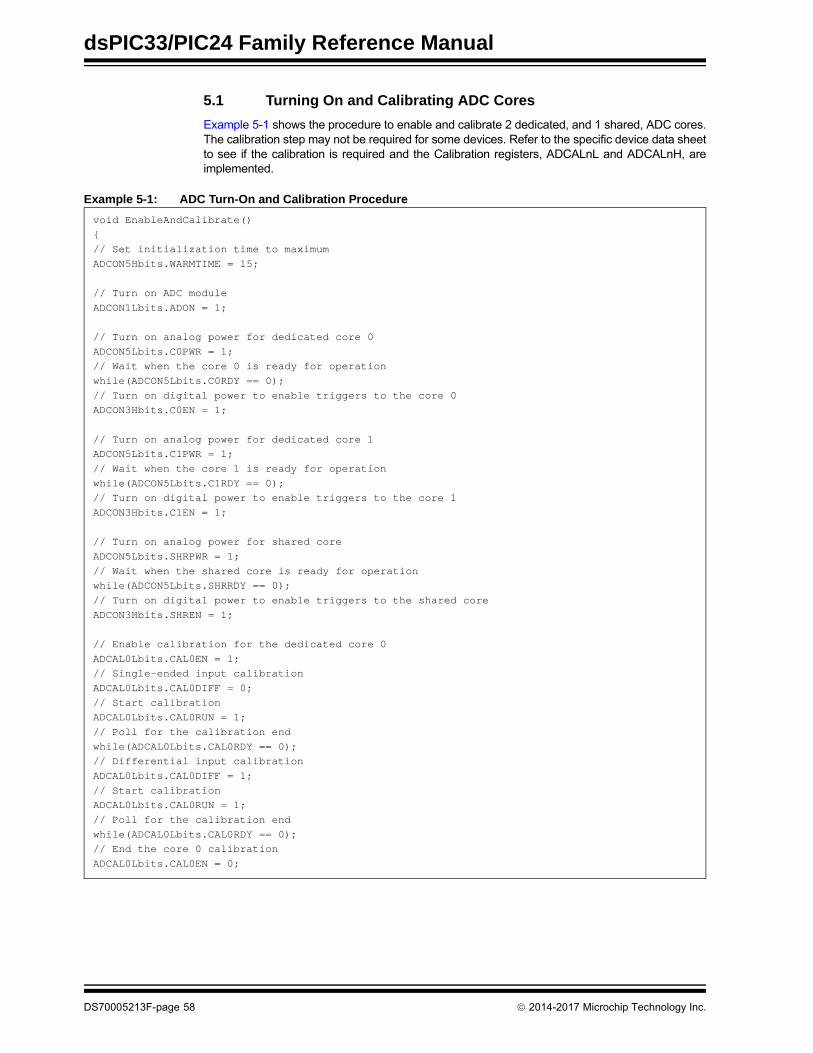
dsPIC33/PIC24 Family Reference Manual
5.1 Turning On and Calibrating ADC Cores
Example 5-1 shows the procedure to enable and calibrate 2 dedicated, and 1 shared, ADC cores.The calibration step may not be required for some devices. Refer to the specific device data sheetto see if the calibration is required and the Calibration registers, ADCALnL and ADCALnH, areimplemented.
Example 5-1: ADC Turn-On and Calibration Procedure
void EnableAndCalibrate(){// Set initialization time to maximumADCON5Hbits.WARMTIME = 15;
// Turn on ADC moduleADCON1Lbits.ADON = 1;
// Turn on analog power for dedicated core 0ADCON5Lbits.C0PWR = 1;// Wait when the core 0 is ready for operationwhile(ADCON5Lbits.C0RDY == 0);// Turn on digital power to enable triggers to the core 0ADCON3Hbits.C0EN = 1;
// Turn on analog power for dedicated core 1ADCON5Lbits.C1PWR = 1;// Wait when the core 1 is ready for operationwhile(ADCON5Lbits.C1RDY == 0);// Turn on digital power to enable triggers to the core 1ADCON3Hbits.C1EN = 1;
// Turn on analog power for shared coreADCON5Lbits.SHRPWR = 1;// Wait when the shared core is ready for operationwhile(ADCON5Lbits.SHRRDY == 0);// Turn on digital power to enable triggers to the shared coreADCON3Hbits.SHREN = 1;
// Enable calibration for the dedicated core 0ADCAL0Lbits.CAL0EN = 1;// Single-ended input calibrationADCAL0Lbits.CAL0DIFF = 0;// Start calibrationADCAL0Lbits.CAL0RUN = 1;// Poll for the calibration endwhile(ADCAL0Lbits.CAL0RDY == 0);// Differential input calibrationADCAL0Lbits.CAL0DIFF = 1;// Start calibrationADCAL0Lbits.CAL0RUN = 1;// Poll for the calibration endwhile(ADCAL0Lbits.CAL0RDY == 0);// End the core 0 calibration ADCAL0Lbits.CAL0EN = 0;
DS70005213F-page 58 2014-2017 Microchip Technology Inc.

12-Bit High-Speed, Multiple SARs A/D Converter (ADC)
Example 5-1: ADC Turn-On and Calibration Procedure (Continued)
// Enable calibration for the dedicated core 1ADCAL0Lbits.CAL1EN = 1;// Single-ended input calibrationADCAL0Lbits.CAL1DIFF = 0;// Start calibrationADCAL0Lbits.CAL1RUN = 1;// Poll for the calibration endwhile(ADCAL0Lbits.CAL1RDY == 0);// Differential input calibrationADCAL0Lbits.CAL1DIFF = 1;// Start calibrationADCAL0Lbits.CAL1RUN = 1;// Poll for the calibration endwhile(ADCAL0Lbits.CAL1RDY == 0);// End the core 1 calibration ADCAL0Lbits.CAL1EN = 0;
// Enable calibration for the shared coreADCAL1Hbits.CSHREN = 1;// Single-ended input calibrationADCAL1Hbits.CSHRDIFF = 0;// Start calibrationADCAL1Hbits.CSHRRUN = 1;// Poll for the calibration endwhile(ADCAL1Hbits.CSHRRDY == 0);// Differential input calibrationADCAL1Hbits.CSHRDIFF = 1;// Start calibrationADCAL1Hbits.CSHRRUN = 1;// Poll for the calibration endwhile(ADCAL1Hbits.CSHRRDY == 0);// End the shared core calibration ADCAL1Hbits.CSHREN = 0;}
2014-2017 Microchip Technology Inc. DS70005213F-page 59
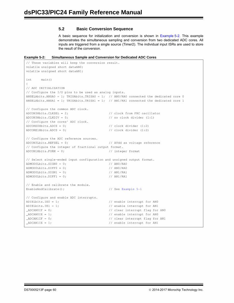
dsPIC33/PIC24 Family Reference Manual
5.2 Basic Conversion Sequence
A basic sequence for initialization and conversion is shown in Example 5-2. This exampledemonstrates the simultaneous sampling and conversion from two dedicated ADC cores. Allinputs are triggered from a single source (Timer2). The individual input ISRs are used to storethe result of the conversion.
Example 5-2: Simultaneous Sample and Conversion for Dedicated ADC Cores
// These variables will keep the conversion result.volatile unsigned short dataAN0;volatile unsigned short dataAN1;
int main(){// ADC INITIALIZATION// Configure the I/O pins to be used as analog inputs.ANSELAbits.ANSA0 = 1; TRISAbits.TRISA0 = 1; // AN0/RA0 connected the dedicated core 0ANSELAbits.ANSA1 = 1; TRISAbits.TRISA1 = 1; // AN1/RA1 connected the dedicated core 1
// Configure the common ADC clock.ADCON3Hbits.CLKSEL = 2; // clock from FRC oscillatorADCON3Hbits.CLKDIV = 0; // no clock divider (1:1)// Configure the cores’ ADC clock.ADCORE0Hbits.ADCS = 0; // clock divider (1:2)ADCORE1Hbits.ADCS = 0; // clock divider (1:2)
// Configure the ADC reference sources.ADCON3Lbits.REFSEL = 0; // AVdd as voltage reference// Configure the integer of fractional output format.ADCON1Hbits.FORM = 0; // integer format
// Select single-ended input configuration and unsigned output format.ADMOD0Lbits.SIGN0 = 0; // AN0/RA0ADMOD0Lbits.DIFF0 = 0; // AN0/RA0ADMOD0Lbits.SIGN1 = 0; // AN1/RA1ADMOD0Lbits.DIFF1 = 0; // AN1/RA1
// Enable and calibrate the module.EnableAndCalibrate(); // See Example 5-1
// Configure and enable ADC interrupts.ADIELbits.IE0 = 1; // enable interrupt for AN0ADIELbits.IE1 = 1; // enable interrupt for AN1_ADCAN0IF = 0; // clear interrupt flag for AN0_ADCAN0IE = 1; // enable interrupt for AN0_ADCAN1IF = 0; // clear interrupt flag for AN1_ADCAN1IE = 1; // enable interrupt for AN1
DS70005213F-page 60 2014-2017 Microchip Technology Inc.
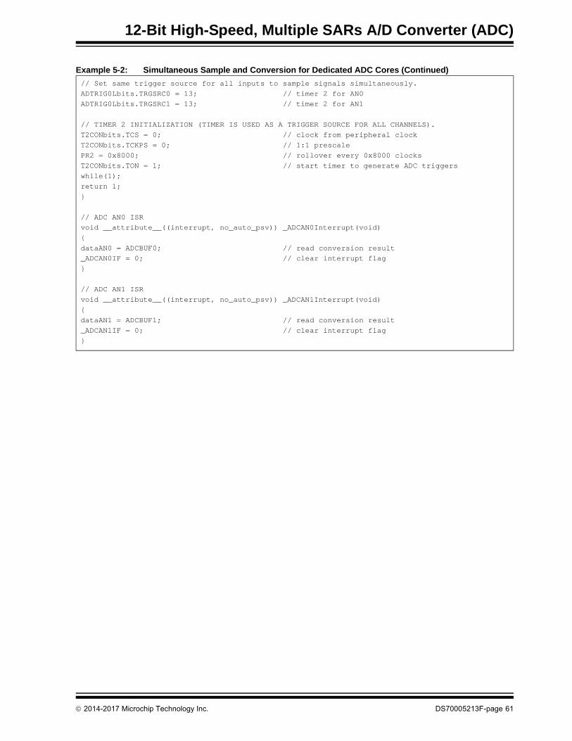
12-Bit High-Speed, Multiple SARs A/D Converter (ADC)
Example 5-2: Simultaneous Sample and Conversion for Dedicated ADC Cores (Continued)
// Set same trigger source for all inputs to sample signals simultaneously.ADTRIG0Lbits.TRGSRC0 = 13; // timer 2 for AN0ADTRIG0Lbits.TRGSRC1 = 13; // timer 2 for AN1
// TIMER 2 INITIALIZATION (TIMER IS USED AS A TRIGGER SOURCE FOR ALL CHANNELS).T2CONbits.TCS = 0; // clock from peripheral clockT2CONbits.TCKPS = 0; // 1:1 prescalePR2 = 0x8000; // rollover every 0x8000 clocksT2CONbits.TON = 1; // start timer to generate ADC triggerswhile(1);return 1;}
// ADC AN0 ISRvoid __attribute__((interrupt, no_auto_psv)) _ADCAN0Interrupt(void){dataAN0 = ADCBUF0; // read conversion result_ADCAN0IF = 0; // clear interrupt flag}
// ADC AN1 ISRvoid __attribute__((interrupt, no_auto_psv)) _ADCAN1Interrupt(void){dataAN1 = ADCBUF1; // read conversion result_ADCAN1IF = 0; // clear interrupt flag}
2014-2017 Microchip Technology Inc. DS70005213F-page 61

dsPIC33/PIC24 Family Reference Manual
5.3 Digital Comparator
The digital comparator allows monitoring selected analog input conversion results. For the digitalcomparator module, the recommended initialization sequence is:
1. Set high and low thresholds in the ADCMPnLO and ADCMPnHI registers in the formatselected for the output data in the ADCBUFx registers.
2. Select analog inputs for the comparison by setting the corresponding bits in theADCMPnENL/H registers.
3. Set the comparator event rules using the BTWN, HIHI, HILO, LOHI and LOLO bits in theADCMPnCON register.
4. Configure and enable the ADC digital comparator interrupt.
5. Set the CMPEN bit in the ADCMPnCON register to enable the comparator.
Example 5-3 demonstrates using the digital comparator to detect voltages for two analog inputsthat are outside the thresholds defined in ADCMPnLO and ADCMPnHI.
Example 5-3: Using the Digital Comparator
// This variable will contain the analog input number// which has generated an event for the digital comparator.volatile unsigned short comparatorChannelNumber;
// These variables will keep the conversion result.volatile unsigned short dataAN0;volatile unsigned short dataAN1;
int main(){// ADC INITIALIZATION// Configure the I/O pins to be used as analog inputs.ANSELAbits.ANSA0 = 1; TRISAbits.TRISA0 = 1; // AN0/RA0 connected the dedicated core 0ANSELAbits.ANSA1 = 1; TRISAbits.TRISA1 = 1; // AN1/RA1 connected the dedicated core 1
// Configure the common ADC clock.ADCON3Hbits.CLKSEL = 2; // clock from FRC oscillatorADCON3Hbits.CLKDIV = 0; // no clock divider (1:1)// Configure the cores’ ADC clock.ADCORE0Hbits.ADCS = 0; // clock divider (1:2)ADCORE1Hbits.ADCS = 0; // clock divider (1:2)
// Configure the ADC reference sources.ADCON3Lbits.REFSEL = 0; // AVdd as voltage reference// Configure the integer of fractional output format.ADCON1Hbits.FORM = 0; // integer format
// Select single-ended input configuration and unsigned output format.ADMOD0Lbits.SIGN0 = 0; // AN0/RA0ADMOD0Lbits.DIFF0 = 0; // AN0/RA0ADMOD0Lbits.SIGN1 = 0; // AN1/RA1ADMOD0Lbits.DIFF1 = 0; // AN1/RA1
// Enable and calibrate the module.EnableAndCalibrate(); // See Example 5-1// Configure and enable ADC interrupts.ADIELbits.IE0 = 1; // enable interrupt for AN0ADIELbits.IE1 = 1; // enable interrupt for AN1_ADCAN0IF = 0; // clear interrupt flag for AN0_ADCAN0IE = 1; // enable interrupt for AN0_ADCAN1IF = 0; // clear interrupt flag for AN1_ADCAN1IE = 1; // enable interrupt for AN1
DS70005213F-page 62 2014-2017 Microchip Technology Inc.
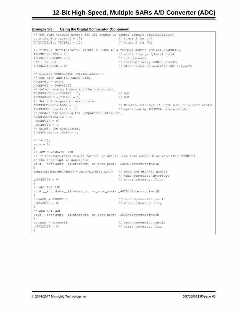
12-Bit High-Speed, Multiple SARs A/D Converter (ADC)
Example 5-3: Using the Digital Comparator (Continued)
// Set same trigger source for all inputs to sample signals simultaneously.ADTRIG0Lbits.TRGSRC0 = 13; // timer 2 for AN0ADTRIG0Lbits.TRGSRC1 = 13; // timer 2 for AN1
// TIMER 2 INITIALIZATION (TIMER IS USED AS A TRIGGER SOURCE FOR ALL CHANNELS).T2CONbits.TCS = 0; // clock from peripheral clockT2CONbits.TCKPS = 0; // 1:1 prescalePR2 = 0x8000; // rollover every 0x8000 clocksT2CONbits.TON = 1; // start timer to generate ADC triggers
// DIGITAL COMPARATOR INITIALIZATION.// Set high and low thresholds.ADCMP0LO = 1024;ADCMP0HI = 4096-1024;// Select analog inputs for the comparison.ADCMP0ENLbits.CMPEN0 = 1; // AN0ADCMP0ENLbits.CMPEN1 = 1; // AN1// Set the comparator event rule.ADCMP0CONbits.LOLO = 1; // Generate interrupt if input level is outside windowADCMP0CONbits.HIHI = 1; // specified by ADCMP0LO and ADCMP0HI.// Enable the ADC Digital Comparator interrupt.ADCMP0CONbits.IE = 1;_ADCMP0IF = 0;_ADCMP0IE = 1;// Enable the comparator.ADCMP0CONbits.CMPEN = 1;
while(1);return 1;}// ADC COMPARATOR ISR// If the conversion result for AN0 or AN1 is less than ADCMP0LO or more than ADCMP0HI,// the interrupt is generatedvoid __attribute__((interrupt, no_auto_psv)) _ADCMP0Interrupt(void){comparatorChannelNumber = ADCMP0CONbits.CHNL; // read the channel number
// that generated interrupt_ADCMP0IF = 0; // clear interrupt flag}// ADC AN0 ISRvoid __attribute__((interrupt, no_auto_psv)) _ADCAN0Interrupt(void){dataAN0 = ADCBUF0; // read conversion result_ADCAN0IF = 0; // clear interrupt flag}// ADC AN1 ISRvoid __attribute__((interrupt, no_auto_psv)) _ADCAN1Interrupt(void){dataAN1 = ADCBUF1; // read conversion result_ADCAN1IF = 0; // clear interrupt flag}
2014-2017 Microchip Technology Inc. DS70005213F-page 63
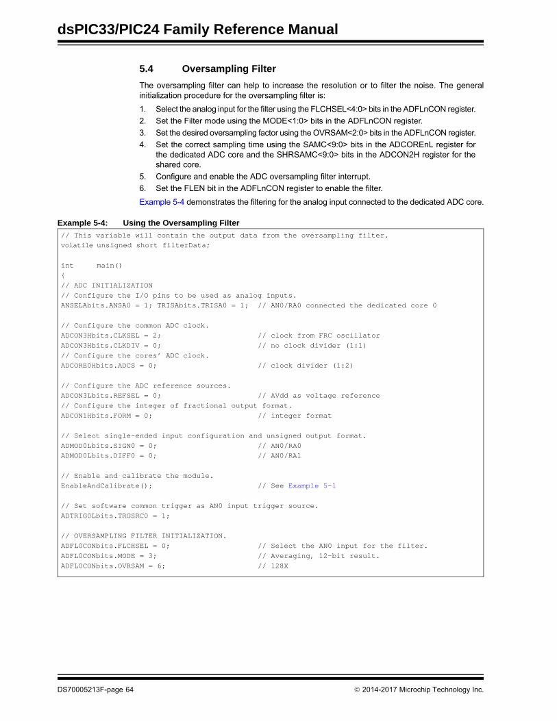
dsPIC33/PIC24 Family Reference Manual
5.4 Oversampling Filter
The oversampling filter can help to increase the resolution or to filter the noise. The generalinitialization procedure for the oversampling filter is:
1. Select the analog input for the filter using the FLCHSEL<4:0> bits in the ADFLnCON register.
2. Set the Filter mode using the MODE<1:0> bits in the ADFLnCON register.
3. Set the desired oversampling factor using the OVRSAM<2:0> bits in the ADFLnCON register.
4. Set the correct sampling time using the SAMC<9:0> bits in the ADCOREnL register forthe dedicated ADC core and the SHRSAMC<9:0> bits in the ADCON2H register for theshared core.
5. Configure and enable the ADC oversampling filter interrupt.
6. Set the FLEN bit in the ADFLnCON register to enable the filter.
Example 5-4 demonstrates the filtering for the analog input connected to the dedicated ADC core.
Example 5-4: Using the Oversampling Filter
// This variable will contain the output data from the oversampling filter.volatile unsigned short filterData;
int main(){// ADC INITIALIZATION// Configure the I/O pins to be used as analog inputs.ANSELAbits.ANSA0 = 1; TRISAbits.TRISA0 = 1; // AN0/RA0 connected the dedicated core 0
// Configure the common ADC clock.ADCON3Hbits.CLKSEL = 2; // clock from FRC oscillatorADCON3Hbits.CLKDIV = 0; // no clock divider (1:1)// Configure the cores’ ADC clock.ADCORE0Hbits.ADCS = 0; // clock divider (1:2)
// Configure the ADC reference sources.ADCON3Lbits.REFSEL = 0; // AVdd as voltage reference// Configure the integer of fractional output format.ADCON1Hbits.FORM = 0; // integer format
// Select single-ended input configuration and unsigned output format.ADMOD0Lbits.SIGN0 = 0; // AN0/RA0ADMOD0Lbits.DIFF0 = 0; // AN0/RA1
// Enable and calibrate the module.EnableAndCalibrate(); // See Example 5-1
// Set software common trigger as AN0 input trigger source.ADTRIG0Lbits.TRGSRC0 = 1; // OVERSAMPLING FILTER INITIALIZATION.ADFL0CONbits.FLCHSEL = 0; // Select the AN0 input for the filter.ADFL0CONbits.MODE = 3; // Averaging, 12-bit result.ADFL0CONbits.OVRSAM = 6; // 128X
DS70005213F-page 64 2014-2017 Microchip Technology Inc.

12-Bit High-Speed, Multiple SARs A/D Converter (ADC)
Example 5-4: Using the Oversampling Filter (Continued)
// Enable delay between trigger and the conversion start (SAMC bits).ADCON4Lbits.SAMC0EN = 1;// Set sampling time (10x Tad)ADCORE0Lbits.SAMC = 10;
// Enable the filter.ADFL0CONbits.FLEN = 1;
while(1){// Generate Software Common TriggerADCON3Lbits.SWCTRG = 1;
// Wait for the filter result is ready.while(ADFL0CONbits.RDY == 0);
// Read result (it will clear RDY bit)filterData = ADFL0DAT;
}
return 1;}
2014-2017 Microchip Technology Inc. DS70005213F-page 65
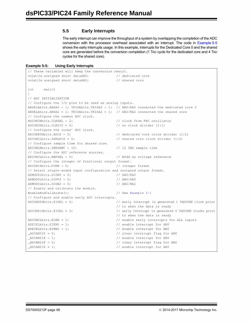
dsPIC33/PIC24 Family Reference Manual
5.5 Early Interrupts
The early interrupt can improve the throughput of a system by overlapping the completion of the ADCconversion with the processor overhead associated with an interrupt. The code in Example 5-5shows the early interrupts usage. In this example, interrupts for the Dedicated Core 0 and the sharedcore are generated before the conversion completion (1 TAD cycle for the dedicated core and 4 TAD
cycles for the shared core).
Example 5-5: Using Early Interrupts
// These variables will keep the conversion result.volatile unsigned short dataAN0; // dedicated corevolatile unsigned short dataAN2; // shared core
int main(){// ADC INITIALIZATION// Configure the I/O pins to be used as analog inputs.ANSELAbits.ANSA0 = 1; TRISAbits.TRISA0 = 1; // AN0/RA0 connected the dedicated core 0ANSELAbits.ANSA2 = 1; TRISAbits.TRISA2 = 1; // AN2/RA2 connected the shared core// Configure the common ADC clock.ADCON3Hbits.CLKSEL = 2; // clock from FRC oscillatorADCON3Hbits.CLKDIV = 0; // no clock divider (1:1)// Configure the cores’ ADC clock.ADCORE0Hbits.ADCS = 0; // dedicated core clock divider (1:2)ADCON2Lbits.SHRADCS = 0; // shared core clock divider (1:2)// Configure sample time for shared core.ADCON2Hbits.SHRSAMC = 10; // 12 TAD sample time // Configure the ADC reference sources.ADCON3Lbits.REFSEL = 0; // AVdd as voltage reference// Configure the integer of fractional output format.ADCON1Hbits.FORM = 0; // integer format// Select single-ended input configuration and unsigned output format.ADMOD0Lbits.SIGN0 = 0; // AN0/RA0ADMOD0Lbits.DIFF0 = 0; // AN0/RA0ADMOD0Lbits.SIGN2 = 0; // AN2/RA2// Enable and calibrate the module.EnableAndCalibrate(); // See Example 5-1// Configure and enable early ADC interrupts.ADCORE0Hbits.EISEL = 0; // early interrupt is generated 1 TADCORE clock prior
// to when the data is readyADCORE1Hbits.EISEL = 3; // early interrupt is generated 4 TADCORE clocks prior
// to when the data is readyADCON2Lbits.EIEN = 1; // enable early interrupts for ALL inputsADEIELbits.EIEN0 = 1; // enable interrupt for AN0ADEIELbits.EIEN2 = 1; // enable interrupt for AN2_ADCAN0IF = 0; // clear interrupt flag for AN0_ADCAN0IE = 1; // enable interrupt for AN0_ADCAN2IF = 0; // clear interrupt flag for AN2_ADCAN2IE = 1; // enable interrupt for AN2
DS70005213F-page 66 2014-2017 Microchip Technology Inc.

12-Bit High-Speed, Multiple SARs A/D Converter (ADC)
Example 5-5: Using Early Interrupts (Continued)// Set same trigger source for all inputs to sample signals simultaneously.ADTRIG0Lbits.TRGSRC0 = 13; // timer 2 for AN0ADTRIG0Hbits.TRGSRC2 = 13; // timer 2 for AN2// TIMER 2 INITIALIZATION (TIMER IS USED AS A TRIGGER SOURCE FOR ALL CHANNELS).T2CONbits.TCS = 0; // clock from peripheral clockT2CONbits.TCKPS = 0; // 1:1 prescalePR2 = 0x8000; // rollover every 0x8000 clocksT2CONbits.TON = 1; // start timer to generate ADC triggers
while(1);
return 1;}
// ADC AN0 ISR (DEDICATED CORE)void __attribute__((interrupt, no_auto_psv)) _ADCAN0Interrupt(void){dataAN0 = ADCBUF0; // read conversion result_ADCAN0IF = 0; // clear interrupt flag}
// ADC AN2 ISR (SHARED CORE)void __attribute__((interrupt, no_auto_psv)) _ADCAN2Interrupt(void){dataAN2 = ADCBUF2; // read conversion result_ADCAN2IF = 0; // clear interrupt flag}
2014-2017 Microchip Technology Inc. DS70005213F-page 67

dsPIC33/PIC24 Family Reference Manual
5.6 Capacitive Voltage Divider (CVD)
The CVD allows measuring a capacitance connected to the ADC input. It can be used to detectan event of touch in touch sensor applications. The sensor capacitance is bigger when thesensor is touched. The code in Example 5-6 shows the CVD feature usage. In this example, CVDscans 2 inputs and Digital Comparator 0 detects when the capacitance is changed on theseinputs (capacitive touch sensor is pressed).
Example 5-6: Using CVD
// These variables will keep the CVD result.volatile short dataAN5CVDSampleA;volatile short dataAN5CVDSampleB;
volatile short dataAN6CVDSampleA;volatile short dataAN6CVDSampleB;volatile short dataCVDResult;
// These variable will contain the CVD input number// for the touched sensor.volatile short comparatorChannelNumber;
int main(){// ADC INITIALIZATION// Configure the I/O pins to be used as analog inputs.// Only shared core inputs support CVD. ANSELBbits.ANSB10 = 1; TRISBbits.TRISB10 = 1; // AN5/RB10 connected the shared dedicated core 0ANSELBbits.ANSB1 = 1; TRISBbits.TRISB1 = 1; // AN6/RB1 connected the dedicated core 1
// Configure the common ADC clock.ADCON3Hbits.CLKSEL = 2; // clock from FRC oscillator (7.3728 MHz)ADCON3Hbits.CLKDIV = 0; // no clock divider (1:1)// Configure the cores’ ADC clock.ADCORE0Hbits.ADCS = 0; // clock divider (1:2)ADCORE1Hbits.ADCS = 0; // clock divider (1:2)ADCON2Lbits.SHRADCS = 0; // clock divider (1:2) for shared core// Configure the ADC reference sources.ADCON3Lbits.REFSEL = 0; // AVdd as voltage reference// Configure the integer of fractional output format.ADCON1Hbits.FORM = 0; // integer format
// Select single-ended input configuration and unsigned output format.ADMOD0Lbits.SIGN5 = 0; // AN5/RB10ADMOD0Lbits.SIGN6 = 0; // AN6/RB1
// Add AN5 and AN6 to CVD scan listADCSSLbits.CSS5 = 1; // AN5ADCSSLbits.CSS6 = 1; // AN6
// Disable all triggers for CVD inputs.// Conversions for these channels will be triggered by CVD.ADTRIG1Lbits.TRGSRC5 = 0; // AN5ADTRIG1Hbits.TRGSRC6 = 0; // AN6
// Select CVD settle time Tsettle = 128*Tad/2 = 128*(2/FRC)/2 = 17uSADCON2Hbits.SHRSAMC = 128-2;
// Enable and calibrate the module.EnableAndCalibrate(); // See Example 5-1
// Configure and enable ADC interrupts.ADIELbits.IE5 = 1; // enable interrupt for AN5ADIELbits.IE6 = 1; // enable interrupt for AN6
DS70005213F-page 68 2014-2017 Microchip Technology Inc.

12-Bit High-Speed, Multiple SARs A/D Converter (ADC)
Example 5-6: Using CVD (Continued)
_ADCAN5IF = 0; // clear interrupt flag for AN5_ADCAN5IE = 1; // enable interrupt for AN5_ADCAN6IF = 0; // clear interrupt flag for AN6_ADCAN6IE = 1; // enable interrupt for AN6
// DIGITAL COMPARATOR INITIALIZATION.// Set high threshold.ADCMP0HI = 2048;// Set the comparator event rule.ADCMP0CONbits.HIHI = 1; // generate event when ADCVDDAT > ADCMP0HI// Enable the ADC Digital Comparator interrupt.ADCMP0CONbits.IE = 1;_ADCMP0IF = 0;_ADCMP0IE = 1;// Enable the comparator.ADCMP0CONbits.CMPEN = 1;
// Scan CVD inputs.ADCON1Lbits.CVDEN = 1;
while(1);return 1;}
// ADC AN5 ISRvoid __attribute__((interrupt, no_auto_psv)) _ADCAN5Interrupt(void){static short sampleA = 0;
sampleA ^= 1; // toggle SampleA flagif(sampleA){dataAN5CVDSampleA = ADCBUF5; // read CVD SampleA result for AN5}else{dataAN5CVDSampleB = ADCBUF5; // read CVD SampleB result for AN5}
_ADCAN5IF = 0; // clear interrupt flag}
// ADC AN6 ISRvoid __attribute__((interrupt, no_auto_psv)) _ADCAN6Interrupt(void){static short sampleA = 0;
sampleA ^= 1; // toggle SampleA flagif(sampleA){dataAN6CVDSampleA = ADCBUF6; // read CVD SampleA result for AN6}else{dataAN6CVDSampleB = ADCBUF6; // read CVD SampleB result for AN6}
_ADCAN6IF = 0; // clear interrupt flag}
// ADC COMPARATOR ISR// If the conversion result for AN5 or AN6 is greater than ADCMP0HI,// the interrupt is generatedvoid __attribute__((interrupt, no_auto_psv)) _ADCMP0Interrupt(void){comparatorChannelNumber = ADCMP0CONbits.CHNL; // read the channel number// that generated interruptdataCVDResult = ADCVDDAT; // read SampleA - SampleB result_ADCMP0IF = 0; // clear interrupt flag}
2014-2017 Microchip Technology Inc. DS70005213F-page 69

dsPIC33/PIC24 Family Reference Manual
6.0 OPERATION DURING POWER-SAVING MODES
The power-saving modes, Sleep and Idle, are useful for reducing the conversion noise byminimizing the digital activity of the CPU, buses and other peripherals.
6.1 Sleep Mode
When a device enters Sleep mode, the system oscillator (FOSC) and all components that operatefrom it are halted. This includes the ADC when FOSC is selected for the clock source. When Sleepmode is invoked during a conversion with FOSC as the clock source, the conversion is aborted.The converter will not resume a partially completed conversion on exiting from Sleep mode. TheADC register contents are not affected by the device entering or leaving Sleep mode.
The ADC module can operate during Sleep mode if the ADC clock source is active during Sleepmode. The FRC oscillator is a logical choice for operation in Sleep mode. ADC operation duringSleep mode reduces the digital switching noise from the rest of the microcontroller during theconversion process.
If any of the ADC interrupts are enabled, the device will wake from Sleep mode when the ADCinterrupt occurs. The program execution will resume at the ADC ISR if the ADC interrupt isgreater than the current CPU priority. Otherwise, execution will continue from the instruction afterthe PWRSAV instruction that placed the device in Sleep mode.
For operation during Sleep mode, the application must use a conversion trigger source thatensures that the A/D conversion will take place in Sleep mode. For example, the external triggerpin option (TRGSRCn<4:0> = 11111) can be used for performing sampling and conversion whilethe device is in Sleep mode.
6.2 Operation During Idle Mode
For the ADC, the Stop in Idle Mode bit, ADSIDL, in the ADCON1L register, specifies whether theADC module will stop on Idle or continue on Idle. If ADSIDL = 0, the ADC module will continuenormal operation when the device enters Idle mode. If any of the ADC interrupts are enabled, thedevice will wake-up from Idle mode when the ADC interrupt occurs. The program execution willresume at the ADC ISR if the ADC interrupt is greater than the current CPU priority. Otherwise,execution will continue from the instruction after the PWRSAV instruction that placed the device inIdle mode.
If ADSIDL = 1, the ADC module will stop in Idle mode. If the device enters Idle mode during aconversion, the conversion is aborted. The converter will not resume a partially completedconversion on exiting from Idle mode.
7.0 EFFECTS OF RESET
Following any Reset event, all the ADC control and status registers are reset to their default val-ues with the control bits in a non-active state. This disables the ADC module and sets the analoginput pins to Analog Input mode. Any conversion that was in progress will be terminated and theresult will not be written to the result buffer. The values in the ADCBUFx registers are initializedto 0000h during a device Reset.
DS70005213F-page 70 2014-2017 Microchip Technology Inc.
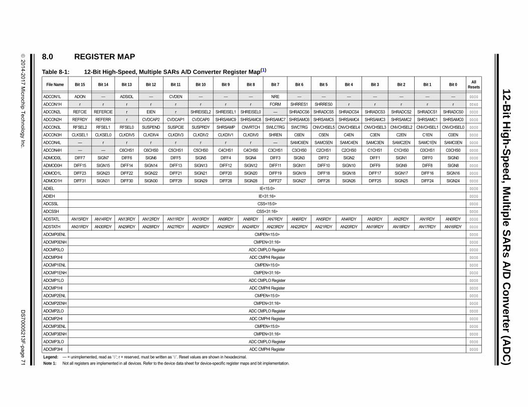
2
01
4-2
01
7 M
icroch
ip T
ech
no
log
y Inc.
DS
70
00
52
13
F-p
ag
e 7
1
12-Bit H
igh
-Sp
eed, M
ultip
le SA
Rs A
/D C
on
verter (AD
C)
8.
Ta
F 3 Bit 2 Bit 1 Bit 0All
Resets
AD — — — 0000
AD r r r 0060
AD DCS3 SHRADCS2 SHRADCS1 SHRADCS0 0000
AD AMC3 SHRSAMC2 SHRSAMC1 SHRSAMC0 0000
AD SEL3 CNVCHSEL2 CNVCHSEL1 CNVCHSEL0 0000
AD N C2EN C1EN C0EN 0000
AD 3EN SAMC2EN SAMC1EN SAMC0EN 0000
AD HS1 C1CHS0 C0CHS1 C0CHS0 0000
AD F1 SIGN1 DIFF0 SIGN0 0000
AD F9 SIGN9 DIFF8 SIGN8 0000
AD 17 SIGN17 DIFF16 SIGN16 0000
AD 25 SIGN25 DIFF24 SIGN24 0000
AD 0000
AD 0000
AD 0000
AD 0000
AD DY AN2RDY AN1RDY AN0RDY 0000
AD RDY AN18RDY AN17RDY AN16RDY 0000
AD 0000
AD 0000
AD 0000
AD 0000
AD 0000
AD 0000
AD 0000
AD 0000
AD 0000
AD 0000
AD 0000
AD 0000
AD 0000
AD 0000
AD 0000
AD 0000
Leg
No
0 REGISTER MAP
ble 8-1: 12-Bit High-Speed, Multiple SARs A/D Converter Register Map(1)
ile Name Bit 15 Bit 14 Bit 13 Bit 12 Bit 11 Bit 10 Bit 9 Bit 8 Bit 7 Bit 6 Bit 5 Bit 4 Bit
CON1L ADON — ADSIDL — CVDEN — — — NRE — — — —
CON1H r r r r r r r r FORM SHRRES1 SHRRES0 r r
CON2L REFCIE REFERCIE r EIEN r SHREISEL2 SHREISEL1 SHREISEL0 — SHRADCS6 SHRADCS5 SHRADCS4 SHRA
CON2H REFRDY REFERR r CVDCAP2 CVDCAP1 CVDCAP0 SHRSAMC9 SHRSAMC8 SHRSAMC7 SHRSAMC6 SHRSAMC5 SHRSAMC4 SHRS
CON3L RFSEL2 RFSEL1 RFSEL0 SUSPEND SUSPCIE SUSPRDY SHRSAMP CNVRTCH SWLCTRG SWCTRG CNVCHSEL5 CNVCHSEL4 CNVCH
CON3H CLKSEL1 CLKSEL0 CLKDIV5 CLKDIV4 CLKDIV3 CLKDIV2 CLKDIV1 CLKDIV0 SHREN C6EN C5EN C4EN C3E
CON4L — r r r r r r r — SAMC6EN SAMC5EN SAMC4EN SAMC
CON4H — — C6CHS1 C6CHS0 C5CHS1 C5CHS0 C4CHS1 C4CHS0 C3CHS1 C3CHS0 C2CHS1 C2CHS0 C1C
MOD0L DIFF7 SIGN7 DIFF6 SIGN6 DIFF5 SIGN5 DIFF4 SIGN4 DIFF3 SIGN3 DIFF2 SIGN2 DIF
MOD0H DIFF15 SIGN15 DIFF14 SIGN14 DIFF13 SIGN13 DIFF12 SIGN12 DIFF11 SIGN11 DIFF10 SIGN10 DIF
MOD1L DIFF23 SIGN23 DIFF22 SIGN22 DIFF21 SIGN21 DIFF20 SIGN20 DIFF19 SIGN19 DIFF18 SIGN18 DIFF
MOD1H DIFF31 SIGN31 DIFF30 SIGN30 DIFF29 SIGN29 DIFF28 SIGN28 DIFF27 SIGN27 DIFF26 SIGN26 DIFF
IEL IE<15:0>
IEH IE<31:16>
CSSL CSS<15:0>
CSSH CSS<31:16>
STATL AN15RDY AN14RDY AN13RDY AN12RDY AN11RDY AN10RDY AN9RDY AN8RDY AN7RDY AN6RDY AN5RDY AN4RDY AN3R
STATH AN31RDY AN30RDY AN29RDY AN28RDY AN27RDY AN26RDY AN25RDY AN24RDY AN23RDY AN22RDY AN21RDY AN20RDY AN19
CMP0ENL CMPEN<15:0>
CMP0ENH CMPEN<31:16>
CMP0LO ADC CMPLO Register
CMP0HI ADC CMPHI Register
CMP1ENL CMPEN<15:0>
CMP1ENH CMPEN<31:16>
CMP1LO ADC CMPLO Register
CMP1HI ADC CMPHI Register
CMP2ENL CMPEN<15:0>
CMP2ENH CMPEN<31:16>
CMP2LO ADC CMPLO Register
CMP2HI ADC CMPHI Register
CMP3ENL CMPEN<15:0>
CMP3ENH CMPEN<31:16>
CMP3LO ADC CMPLO Register
CMP3HI ADC CMPHI Register
end: — = unimplemented, read as ‘0’; r = reserved, must be written as ‘0’. Reset values are shown in hexadecimal.
te 1: Not all registers are implemented in all devices. Refer to the device data sheet for device-specific register maps and bit implementation.

dsP
IC33/P
IC24 F
amily R
eference M
anu
al
DS
70
00
52
13
F-p
ag
e 7
2
20
14
-20
17
Micro
chip
Te
chn
olo
gy In
c.
0000
0000
0000
0000
0000
0000
0000
0000
0000
FLCHSEL3 FLCHSEL2 FLCHSEL1 FLCHSEL0 0000
0000
FLCHSEL3 FLCHSEL2 FLCHSEL1 FLCHSEL0 0000
0000
FLCHSEL3 FLCHSEL2 FLCHSEL1 FLCHSEL0 0000
0000
FLCHSEL3 FLCHSEL2 FLCHSEL1 FLCHSEL0 0000
0000
FLCHSEL3 FLCHSEL2 FLCHSEL1 FLCHSEL0 0000
0000
FLCHSEL3 FLCHSEL2 FLCHSEL1 FLCHSEL0 0000
TRGSRC03 TRGSRC02 TRGSRC01 TRGSRC00 0000
TRGSRC23 TRGSRC22 TRGSRC21 TRGSRC20 0000
TRGSRC43 TRGSRC42 TRGSRC41 TRGSRC40 0000
TRGSRC63 TRGSRC62 TRGSRC61 TRGSRC60 0000
TRGSRC83 TRGSRC82 TRGSRC81 TRGSRC80 0000
RGSRC103 TRGSRC102 TRGSRC101 TRGSRC100 0000
RGSRC123 TRGSRC122 TRGSRC121 TRGSRC120 0000
RGSRC143 TRGSRC142 TRGSRC141 TRGSRC140 0000
RGSRC163 TRGSRC162 TRGSRC161 TRGSRC160 0000
RGSRC183 TRGSRC182 TRGSRC181 TRGSRC180 0000
RGSRC203 TRGSRC202 TRGSRC201 TRGSRC200 0000
RGSRC223 TRGSRC222 TRGSRC221 TRGSRC220 0000
RGSRC243 TRGSRC242 TRGSRC241 TRGSRC240 0000
RGSRC263 TRGSRC262 TRGSRC261 TRGSRC260 0000
Bit 3 Bit 2 Bit 1 Bit 0All
Resets
ADCMP4ENL CMPEN<15:0>
ADCMP4ENH CMPEN<31:16>
ADCMP4LO ADC CMPLO Register
ADCMP4HI ADC CMPHI Register
ADCMP5ENL CMPEN<15:0>
ADCMP5ENH CMPEN<31:16>
ADCMP5LO ADC CMPLO Register
ADCMP5HI ADC CMPHI Register
ADFL0DAT ADC FLDATA Register
ADFL0CON FLEN MODE1 MODE0 OVRSAM2 OVRSAM1 OVRSAM0 IE RDY — — — FLCHSEL4
ADFL1DAT ADC FLDATA Register
ADFL1CON FLEN MODE1 MODE0 OVRSAM2 OVRSAM1 OVRSAM0 IE RDY — — — FLCHSEL4
ADFL2DAT ADC FLDATA Register
ADFL2CON FLEN MODE1 MODE0 OVRSAM2 OVRSAM1 OVRSAM0 IE RDY — — — FLCHSEL4
ADFL3DAT ADC FLDATA Register
ADFL3CON FLEN MODE1 MODE0 OVRSAM2 OVRSAM1 OVRSAM0 IE RDY — — — FLCHSEL4
ADFL4DAT ADC FLDATA Register
ADFL4CON FLEN MODE1 MODE0 OVRSAM2 OVRSAM1 OVRSAM0 IE RDY — — — FLCHSEL4
ADFL5DAT ADC FLDATA Register
ADFL5CON FLEN MODE1 MODE0 OVRSAM2 OVRSAM1 OVRSAM0 IE RDY — — — FLCHSEL4
ADTRIG0L — — — TRGSRC14 TRGSRC13 TRGSRC12 TRGSRC11 TRGSRC10 — — — TRGSRC04
ADTRIG0H — — — TRGSRC34 TRGSRC33 TRGSRC32 TRGSRC31 TRGSRC30 — — — TRGSRC24
ADTRIG1L — — — TRGSRC54 TRGSRC53 TRGSRC52 TRGSRC51 TRGSRC50 — — — TRGSRC44
ADTRIG1H — — — TRGSRC74 TRGSRC73 TRGSRC72 TRGSRC71 TRGSRC70 — — — TRGSRC64
ADTRIG2L — — — TRGSRC94 TRGSRC93 TRGSRC92 TRGSRC91 TRGSRC90 — — — TRGSRC84
ADTRIG2H — — — TRGSRC114 TRGSRC113 TRGSRC112 TRGSRC111 TRGSRC110 — — — TRGSRC104 T
ADTRIG3L — — — TRGSRC134 TRGSRC133 TRGSRC132 TRGSRC131 TRGSRC130 — — — TRGSRC124 T
ADTRIG3H — — — TRGSRC154 TRGSRC153 TRGSRC152 TRGSRC151 TRGSRC150 — — — TRGSRC144 T
ADTRIG4L — — — TRGSRC174 TRGSRC173 TRGSRC172 TRGSRC171 TRGSRC170 — — — TRGSRC164 T
ADTRIG4H — — — TRGSRC194 TRGSRC193 TRGSRC192 TRGSRC191 TRGSRC190 — — — TRGSRC184 T
ADTRIG5L — — — TRGSRC214 TRGSRC213 TRGSRC212 TRGSRC211 TRGSRC210 — — — TRGSRC204 T
ADTRIG5H — — — TRGSRC234 TRGSRC233 TRGSRC232 TRGSRC231 TRGSRC230 — — — TRGSRC224 T
ADTRIG6L — — — TRGSRC254 TRGSRC253 TRGSRC252 TRGSRC251 TRGSRC250 — — — TRGSRC244 T
ADTRIG6H — — — TRGSRC274 TRGSRC273 TRGSRC272 TRGSRC271 TRGSRC270 — — — TRGSRC264 T
Table 8-1: 12-Bit High-Speed, Multiple SARs A/D Converter Register Map(1) (Continued)
File Name Bit 15 Bit 14 Bit 13 Bit 12 Bit 11 Bit 10 Bit 9 Bit 8 Bit 7 Bit 6 Bit 5 Bit 4
Legend: — = unimplemented, read as ‘0’; r = reserved, must be written as ‘0’. Reset values are shown in hexadecimal.
Note 1: Not all registers are implemented in all devices. Refer to the device data sheet for device-specific register maps and bit implementation.

2
01
4-2
01
7 M
icroch
ip T
ech
no
log
y Inc.
DS
70
00
52
13
F-p
ag
e 7
3
12-Bit H
igh
-Sp
eed, M
ultip
le SA
Rs A
/D C
on
verter (AD
C)
AD RC283 TRGSRC282 TRGSRC281 TRGSRC280 0000
AD RC303 TRGSRC302 TRGSRC301 TRGSRC300 0000
AD IHI HILO LOHI LOLO 0000
AD 0000
AD IHI HILO LOHI LOLO 0000
AD IHI HILO LOHI LOLO 0000
AD IHI HILO LOHI LOLO 0000
AD IHI HILO LOHI LOLO 0000
AD IHI HILO LOHI LOLO 0000
AD 0000
AD 0000
AD 0000
AD CS3 ADCS2 ADCS1 ADCS0 0300
AD 0000
AD CS3 ADCS2 ADCS1 ADCS0 0300
AD 0000
AD CS3 ADCS2 ADCS1 ADCS0 0300
AD 0000
AD CS3 ADCS2 ADCS1 ADCS0 0300
AD 0000
AD CS3 ADCS2 ADCS1 ADCS0 0300
AD 0000
AD CS3 ADCS2 ADCS1 ADCS0 0300
AD 0000
AD CS3 ADCS2 ADCS1 ADCS0 0300
AD 0000
AD 0000
AD 0000
AD 0000
AD PWR C2PWR C1PWR C0PWR 0000
AD 3CIE C2CIE C1CIE C0CIE 0000
AD r CAL0DIFF CAL0EN CAL0RUN 0000
AD r CAL2DIFF CAL2EN CAL2RUN 0000
AD r CAL4DIFF CAL4EN CAL4RUN 0000
AD r CAL6DIFF CAL6EN CAL6RUN 0000
Ta
F it 3 Bit 2 Bit 1 Bit 0All
Resets
Leg
No
TRIG7L — — — TRGSRC294 TRGSRC293 TRGSRC292 TRGSRC291 TRGSRC290 — — — TRGSRC284 TRGS
TRIG7H — — — TRGSRC314 TRGSRC313 TRGSRC312 TRGSRC311 TRGSRC310 — — — TRGSRC304 TRGS
CMP0CON — — — CHNL4 CHNL3 CHNL2 CHNL1 CHNL0 CMPEN IE STAT BTWN H
CVDDAT ADCVDDAT<15:0>
CMP1CON — — — CHNL4 CHNL3 CHNL2 CHNL1 CHNL0 CMPEN IE STAT BTWN H
CMP2CON — — — CHNL4 CHNL3 CHNL2 CHNL1 CHNL0 CMPEN IE STAT BTWN H
CMP3CON — — — CHNL4 CHNL3 CHNL2 CHNL1 CHNL0 CMPEN IE STAT BTWN H
CMP4CON — — — CHNL4 CHNL3 CHNL2 CHNL1 CHNL0 CMPEN IE STAT BTWN H
CMP5CON — — — CHNL4 CHNL3 CHNL2 CHNL1 CHNL0 CMPEN IE STAT BTWN H
LVLTRGL LVLEN<15:0>
LVLTRGH LVLEN<31:16>
CORE0L — — — — — — — SAMC<9:0>
CORE0H — — — — — — RES1 RES0 — ADCS6 ADCS5 ADCS4 AD
CORE1L — — — — — — — SAMC<9:0>
CORE1H — — — EISEL2 EISEL1 EISEL0 RES1 RES0 — ADCS6 ADCS5 ADCS4 AD
CORE2L — — — — — — — SAMC<9:0>
CORE2H — — — EISEL2 EISEL1 EISEL0 RES1 RES0 — ADCS6 ADCS5 ADCS4 AD
CORE3L — — — — — — — SAMC<9:0>
CORE3H — — — EISEL2 EISEL1 EISEL0 RES1 RES0 — ADCS6 ADCS5 ADCS4 AD
CORE4L — — — — — — — SAMC<9:0>
CORE4H — — — EISEL2 EISEL1 EISEL0 RES1 RES0 — ADCS6 ADCS5 ADCS4 AD
CORE5L — — — — — — — SAMC<9:0>
CORE5H — — — EISEL2 EISEL1 EISEL0 RES1 RES0 — ADCS6 ADCS5 ADCS4 AD
CORE6L — — — — — — — SAMC<9:0>
CORE6H — — — EISEL2 EISEL1 EISEL0 RES1 RES0 — ADCS6 ADCS5 ADCS4 AD
EIEL EIE<15:0>
EIEH EIE<31:16>
EISTATL EISTAT<15:0>
EISTATH EISTAT<31:16>
CON5L SHRRDY C6RDY C5RDY C4RDY C3RDY C2RDY C1RDY C0RDY SHRPWR C6PWR C5PWR C4PWR C3
CON5H — — — — WARMTIME3 WARMTIME2 WARMTIME1 WARMTIME0 SHRCIE C6CIE C5CIE C4CIE C
CAL0L CAL1RDY — — — r CAL1DIFF CAL1EN CAL1RUN CAL0RDY — — —
CAL0H CAL3RDY — — — r CAL3DIFF CAL3EN CAL3RUN CAL2RDY — — —
CAL1L CAL5RDY — — — r CAL5DIFF CAL5EN CAL5RUN CAL4RDY — — —
CAL1H CSHRRDY — — — r CSHRDIFF CSHREN CSHRRUN CAL6RDY — — —
ble 8-1: 12-Bit High-Speed, Multiple SARs A/D Converter Register Map(1) (Continued)
ile Name Bit 15 Bit 14 Bit 13 Bit 12 Bit 11 Bit 10 Bit 9 Bit 8 Bit 7 Bit 6 Bit 5 Bit 4 B
end: — = unimplemented, read as ‘0’; r = reserved, must be written as ‘0’. Reset values are shown in hexadecimal.
te 1: Not all registers are implemented in all devices. Refer to the device data sheet for device-specific register maps and bit implementation.

dsP
IC33/P
IC24 F
amily R
eference M
anu
al
DS
70
00
52
13
F-p
ag
e 7
4
20
14
-20
17
Micro
chip
Te
chn
olo
gy In
c.
0000
0000
0000
0000
0000
0000
0000
0000
0000
0000
0000
0000
0000
0000
0000
0000
0000
0000
0000
0000
0000
0000
0000
0000
0000
0000
0000
0000
0000
0000
0000
0000
Bit 3 Bit 2 Bit 1 Bit 0All
Resets
ADCBUF0 DATA0<15:0>
ADCBUF1 DATA1<15:0>
ADCBUF2 DATA2<15:0>
ADCBUF3 DATA3<15:0>
ADCBUF4 DATA4<15:0>
ADCBUF5 DATA5<15:0>
ADCBUF6 DATA6<15:0>
ADCBUF7 DATA7<15:0>
ADCBUF8 DATA8<15:0>
ADCBUF9 DATA9<15:0>
ADCBUF10 DATA10<15:0>
ADCBUF11 DATA11<15:0>
ADCBUF12 DATA12<15:0>
ADCBUF13 DATA13<15:0>
ADCBUF14 DATA14<15:0>
ADCBUF15 DATA15<15:0>
ADCBUF16 DATA16<15:0>
ADCBUF17 DATA17<15:0>
ADCBUF18 DATA18<15:0>
ADCBUF19 DATA19<15:0>
ADCBUF20 DATA20<15:0>
ADCBUF21 DATA21<15:0>
ADCBUF22 DATA22<15:0>
ADCBUF23 DATA23<15:0>
ADCBUF24 DATA24<15:0>
ADCBUF25 DATA25<15:0>
ADCBUF26 DATA26<15:0>
ADCBUF27 DATA27<15:0>
ADCBUF28 DATA28<15:0>
ADCBUF29 DATA29<15:0>
ADCBUF30 DATA30<15:0>
ADCBUF31 DATA31<15:0>
Table 8-1: 12-Bit High-Speed, Multiple SARs A/D Converter Register Map(1) (Continued)
File Name Bit 15 Bit 14 Bit 13 Bit 12 Bit 11 Bit 10 Bit 9 Bit 8 Bit 7 Bit 6 Bit 5 Bit 4
Legend: — = unimplemented, read as ‘0’; r = reserved, must be written as ‘0’. Reset values are shown in hexadecimal.
Note 1: Not all registers are implemented in all devices. Refer to the device data sheet for device-specific register maps and bit implementation.

12-Bit High-Speed, Multiple SARs A/D Converter (ADC)
9.0 RELATED APPLICATION NOTES
This section lists application notes that are related to this section of the manual. These applicationnotes may not be written specifically for the dsPIC33/PIC24 device families, but the concepts arepertinent and could be used with modification and possible limitations. The current applicationnotes related to the 12-Bit High-Speed, Multiple SARs A/D Converter (ADC) module are:
Title Application Note #
No related application notes at this time.
Note: Please visit the Microchip web site (www.microchip.com) for additional applicationnotes and code examples for the dsPIC33/PIC24 families of devices.
2014-2017 Microchip Technology Inc. DS70005213F-page 75

dsPIC33/PIC24 Family Reference Manual
10.0 REVISION HISTORY
Revision A (November 2014)
This is the initial revision of this document.
Revision B (May 2015)
Updated Section 4.4 “Sampling and Conversion Timing” and added Equation 4-1.
Revision C (September 2015)
Changed all occurrences of Differential Inputs to Pseudodifferential Inputs. Removed allreferences to CALxSKIP bits.
Updated Figure 1-2, Figure 4-5, Figure 4-6 and Figure 4-10.
Updated Register 2-1, Register 2-2, Register 2-3, Register 2-4, Register 2-7, Register 2-27,Register 2-28, Register 2-29, Register 2-30 and Register 2-31.
Updated Table 4-1 and Table 8-1.
This revision also includes numerous grammatical corrections throughout the document.
Revision D (January 2016)
Updated Figure 4-12 and Figure 4-13.
Updated Section 4.6.3 “Selecting Analog Input for Dedicated ADC Core” andSection 4.13.3 “Early Interrupts”, and added Section 5.5 “Early Interrupts”.
Revision E (January 2017)
Updated Register 2-5, Register 2-7, Register 2-27, Register 2-31 and Register 2-35.
Removed Asynchronous from the Figure 4-2 title.
Removed Figure 4-3 and added new paragraph before Figure 4-4.
Added additional content to Note in Section 4.6.3 “Selecting Analog Input for Dedicated ADCCore”.
Updated the steps to enable the ADC module in Section 4.7 “Enabling the ADC”.
Updated Table 8-1.
Revision F (June 2017)
Updated Section 1.0 “Introduction”, Section 2.1 “Control Registers”, Section 2.2 “DataRegisters” and Section 4.4 “Sampling and Conversion Timing”. Added Section 4.14“Capacitive Voltage Divider (CVD)” and Section 5.6 “Capacitive Voltage Divider (CVD)”.
Updated Register 2-1 and Register 2-4. Added Register 2-36 and Register 2-37.
Added Figure 4-14.
Added Equation 4-2.
Added Example 5-6.
Updated Table 8-1.
DS70005213F-page 76 2014-2017 Microchip Technology Inc.

Note the following details of the code protection feature on Microchip devices:
• Microchip products meet the specification contained in their particular Microchip Data Sheet.
• Microchip believes that its family of products is one of the most secure families of its kind on the market today, when used in the intended manner and under normal conditions.
• There are dishonest and possibly illegal methods used to breach the code protection feature. All of these methods, to our knowledge, require using the Microchip products in a manner outside the operating specifications contained in Microchip’s Data Sheets. Most likely, the person doing so is engaged in theft of intellectual property.
• Microchip is willing to work with the customer who is concerned about the integrity of their code.
• Neither Microchip nor any other semiconductor manufacturer can guarantee the security of their code. Code protection does not mean that we are guaranteeing the product as “unbreakable.”
Code protection is constantly evolving. We at Microchip are committed to continuously improving the code protection features of ourproducts. Attempts to break Microchip’s code protection feature may be a violation of the Digital Millennium Copyright Act. If such actsallow unauthorized access to your software or other copyrighted work, you may have a right to sue for relief under that Act.
Information contained in this publication regarding deviceapplications and the like is provided only for your convenienceand may be superseded by updates. It is your responsibility toensure that your application meets with your specifications.MICROCHIP MAKES NO REPRESENTATIONS ORWARRANTIES OF ANY KIND WHETHER EXPRESS ORIMPLIED, WRITTEN OR ORAL, STATUTORY OROTHERWISE, RELATED TO THE INFORMATION,INCLUDING BUT NOT LIMITED TO ITS CONDITION,QUALITY, PERFORMANCE, MERCHANTABILITY ORFITNESS FOR PURPOSE. Microchip disclaims all liabilityarising from this information and its use. Use of Microchipdevices in life support and/or safety applications is entirely atthe buyer’s risk, and the buyer agrees to defend, indemnify andhold harmless Microchip from any and all damages, claims,suits, or expenses resulting from such use. No licenses areconveyed, implicitly or otherwise, under any Microchipintellectual property rights unless otherwise stated.
2014-2017 Microchip Technology Inc.
Microchip received ISO/TS-16949:2009 certification for its worldwide headquarters, design and wafer fabrication facilities in Chandler and Tempe, Arizona; Gresham, Oregon and design centers in California and India. The Company’s quality system processes and procedures are for its PIC® MCUs and dsPIC® DSCs, KEELOQ® code hopping devices, Serial EEPROMs, microperipherals, nonvolatile memory and analog products. In addition, Microchip’s quality system for the design and manufacture of development systems is ISO 9001:2000 certified.
QUALITY MANAGEMENT SYSTEM CERTIFIED BY DNV
== ISO/TS 16949 ==
Trademarks
The Microchip name and logo, the Microchip logo, AnyRate, AVR, AVR logo, AVR Freaks, BeaconThings, BitCloud, CryptoMemory, CryptoRF, dsPIC, FlashFlex, flexPWR, Heldo, JukeBlox, KEELOQ, KEELOQ logo, Kleer, LANCheck, LINK MD, maXStylus, maXTouch, MediaLB, megaAVR, MOST, MOST logo, MPLAB, OptoLyzer, PIC, picoPower, PICSTART, PIC32 logo, Prochip Designer, QTouch, RightTouch, SAM-BA, SpyNIC, SST, SST Logo, SuperFlash, tinyAVR, UNI/O, and XMEGA are registered trademarks of Microchip Technology Incorporated in the U.S.A. and other countries.
ClockWorks, The Embedded Control Solutions Company, EtherSynch, Hyper Speed Control, HyperLight Load, IntelliMOS, mTouch, Precision Edge, and Quiet-Wire are registered trademarks of Microchip Technology Incorporated in the U.S.A.
Adjacent Key Suppression, AKS, Analog-for-the-Digital Age, Any Capacitor, AnyIn, AnyOut, BodyCom, chipKIT, chipKIT logo, CodeGuard, CryptoAuthentication, CryptoCompanion, CryptoController, dsPICDEM, dsPICDEM.net, Dynamic Average Matching, DAM, ECAN, EtherGREEN, In-Circuit Serial Programming, ICSP, Inter-Chip Connectivity, JitterBlocker, KleerNet, KleerNet logo, Mindi, MiWi, motorBench, MPASM, MPF, MPLAB Certified logo, MPLIB, MPLINK, MultiTRAK, NetDetach, Omniscient Code Generation, PICDEM, PICDEM.net, PICkit, PICtail, PureSilicon, QMatrix, RightTouch logo, REAL ICE, Ripple Blocker, SAM-ICE, Serial Quad I/O, SMART-I.S., SQI, SuperSwitcher, SuperSwitcher II, Total Endurance, TSHARC, USBCheck, VariSense, ViewSpan, WiperLock, Wireless DNA, and ZENA are trademarks of Microchip Technology Incorporated in the U.S.A. and other countries.
SQTP is a service mark of Microchip Technology Incorporated in the U.S.A.
Silicon Storage Technology is a registered trademark of Microchip Technology Inc. in other countries.
GestIC is a registered trademark of Microchip Technology Germany II GmbH & Co. KG, a subsidiary of Microchip Technology Inc., in other countries.
All other trademarks mentioned herein are property of their respective companies.
© 2014-2017, Microchip Technology Incorporated, All Rights Reserved.
ISBN: 978-1-5224-1830-6
DS70005213F-page 77

DS70005213F-page 78 2014-2017 Microchip Technology Inc.
AMERICASCorporate Office2355 West Chandler Blvd.Chandler, AZ 85224-6199Tel: 480-792-7200 Fax: 480-792-7277Technical Support: http://www.microchip.com/supportWeb Address: www.microchip.com
AtlantaDuluth, GA Tel: 678-957-9614 Fax: 678-957-1455
Austin, TXTel: 512-257-3370
BostonWestborough, MA Tel: 774-760-0087 Fax: 774-760-0088
ChicagoItasca, IL Tel: 630-285-0071 Fax: 630-285-0075
DallasAddison, TX Tel: 972-818-7423 Fax: 972-818-2924
DetroitNovi, MI Tel: 248-848-4000
Houston, TX Tel: 281-894-5983
IndianapolisNoblesville, IN Tel: 317-773-8323Fax: 317-773-5453Tel: 317-536-2380
Los AngelesMission Viejo, CA Tel: 949-462-9523Fax: 949-462-9608Tel: 951-273-7800
Raleigh, NC Tel: 919-844-7510
New York, NY Tel: 631-435-6000
San Jose, CA Tel: 408-735-9110Tel: 408-436-4270
Canada - TorontoTel: 905-695-1980 Fax: 905-695-2078
ASIA/PACIFICAsia Pacific OfficeSuites 3707-14, 37th FloorTower 6, The GatewayHarbour City, Kowloon
Hong KongTel: 852-2943-5100Fax: 852-2401-3431
Australia - SydneyTel: 61-2-9868-6733Fax: 61-2-9868-6755
China - BeijingTel: 86-10-8569-7000 Fax: 86-10-8528-2104
China - ChengduTel: 86-28-8665-5511Fax: 86-28-8665-7889
China - ChongqingTel: 86-23-8980-9588Fax: 86-23-8980-9500
China - DongguanTel: 86-769-8702-9880
China - GuangzhouTel: 86-20-8755-8029
China - HangzhouTel: 86-571-8792-8115 Fax: 86-571-8792-8116
China - Hong Kong SARTel: 852-2943-5100 Fax: 852-2401-3431
China - NanjingTel: 86-25-8473-2460Fax: 86-25-8473-2470
China - QingdaoTel: 86-532-8502-7355Fax: 86-532-8502-7205
China - ShanghaiTel: 86-21-3326-8000 Fax: 86-21-3326-8021
China - ShenyangTel: 86-24-2334-2829Fax: 86-24-2334-2393
China - ShenzhenTel: 86-755-8864-2200 Fax: 86-755-8203-1760
China - WuhanTel: 86-27-5980-5300Fax: 86-27-5980-5118
China - XianTel: 86-29-8833-7252Fax: 86-29-8833-7256
ASIA/PACIFICChina - XiamenTel: 86-592-2388138 Fax: 86-592-2388130
China - ZhuhaiTel: 86-756-3210040 Fax: 86-756-3210049
India - BangaloreTel: 91-80-3090-4444 Fax: 91-80-3090-4123
India - New DelhiTel: 91-11-4160-8631Fax: 91-11-4160-8632
India - PuneTel: 91-20-3019-1500
Japan - OsakaTel: 81-6-6152-7160 Fax: 81-6-6152-9310
Japan - TokyoTel: 81-3-6880- 3770 Fax: 81-3-6880-3771
Korea - DaeguTel: 82-53-744-4301Fax: 82-53-744-4302
Korea - SeoulTel: 82-2-554-7200Fax: 82-2-558-5932 or 82-2-558-5934
Malaysia - Kuala LumpurTel: 60-3-6201-9857Fax: 60-3-6201-9859
Malaysia - PenangTel: 60-4-227-8870Fax: 60-4-227-4068
Philippines - ManilaTel: 63-2-634-9065Fax: 63-2-634-9069
SingaporeTel: 65-6334-8870Fax: 65-6334-8850
Taiwan - Hsin ChuTel: 886-3-5778-366Fax: 886-3-5770-955
Taiwan - KaohsiungTel: 886-7-213-7830
Taiwan - TaipeiTel: 886-2-2508-8600 Fax: 886-2-2508-0102
Thailand - BangkokTel: 66-2-694-1351Fax: 66-2-694-1350
EUROPEAustria - WelsTel: 43-7242-2244-39Fax: 43-7242-2244-393
Denmark - CopenhagenTel: 45-4450-2828 Fax: 45-4485-2829
Finland - EspooTel: 358-9-4520-820
France - ParisTel: 33-1-69-53-63-20 Fax: 33-1-69-30-90-79
France - Saint CloudTel: 33-1-30-60-70-00
Germany - GarchingTel: 49-8931-9700Germany - HaanTel: 49-2129-3766400
Germany - HeilbronnTel: 49-7131-67-3636
Germany - KarlsruheTel: 49-721-625370
Germany - MunichTel: 49-89-627-144-0 Fax: 49-89-627-144-44
Germany - RosenheimTel: 49-8031-354-560
Israel - Ra’anana Tel: 972-9-744-7705
Italy - Milan Tel: 39-0331-742611 Fax: 39-0331-466781
Italy - PadovaTel: 39-049-7625286
Netherlands - DrunenTel: 31-416-690399 Fax: 31-416-690340
Norway - TrondheimTel: 47-7289-7561
Poland - WarsawTel: 48-22-3325737
Romania - BucharestTel: 40-21-407-87-50
Spain - MadridTel: 34-91-708-08-90Fax: 34-91-708-08-91
Sweden - GothenbergTel: 46-31-704-60-40
Sweden - StockholmTel: 46-8-5090-4654
UK - WokinghamTel: 44-118-921-5800Fax: 44-118-921-5820
Worldwide Sales and Service
11/07/16