1111111111111111111111111111111111111111111111111111111111 ... › drp-published-uspatents ›...
37
111111111111111111111111111111111111111111111111111111111111111111111111111111111111111111 us 20070189431Al (19) United States (12) Patent Application Publication Waheed et al. (10) Pub. No.: US 2007/0189431 Al (43) Pub. Date: Aug. 16,2007 (54) DELAY ALIGNMENT IN A CLOSED LOOP TWO-POINT MODULATION ALL DIGITAL PHASE LOCKED LOOP Correspondence Address: TEXAS INSTRUMENTS INCORPORATED POBOX 655474, MIS 3999 DALLAS, TX 75265 Related U.S. Application Data (60) Provisional application No. 601773,759, filed on Feb. 15, 2006. (75) Inventors: (73) Assignee: (21) Appl. No.: (22) Filed: Khurram Waheed, Plano, TX (US); Tim Foo, Plano, TX (US); Robert B. Staszewski, Garland, TX (US) Texas Instruments Incorporated 111675,573 Feb. 15, 2007 Publication Classification (51) Int. Cl. H03D 3/24 (2006.01) H04L 27/04 (2006.01) (52) U.S. Cl. 375/376; 375/300 (57) ABSTRACT A novel apparatus for and method of delay alignment in a closed loop two-point modulation all digital phase locked loop (ADPLL). The invention provides a fully digital delay alignment mechanism where better than nanosecond align- ment is achieved by accounting for processing delays in the digital circuit modules of the transmitter and by the use of progral11l11able delay elements spread across several clock domains. Tapped delay lines compensate for propagation and settling delays in analog elements such as the DCO, dividers, quad switch, buffers, level shifters and digital pre-power amplifier (DPA). A signal correlative mechanism is provided whereby data from the amplitude and phasel frequency modulation paths to be matched is first interpo- lated and then cross-correlated to achieve accuracy better than the clock domain of comparison. Within the ADPLL portion of the transmitter, precise alignment of reference and direct point injection points in the ADPLL is provided using multiple clock domains, tapped delay lines and clock adjust- ment circuits. 1----------------------------------------------1 I I I J y'[k]1 x[i] 558 CV ,--, I I I I I I I I I CKVDx= CKVIx : : L __ CKR 566 FREF DATA PATH L 521 y'[k] (FM I f FCW_CH : J y'[k] RJ-,fL 549 K DCO
Transcript of 1111111111111111111111111111111111111111111111111111111111 ... › drp-published-uspatents ›...

111111111111111111111111111111111111111111111111111111111111111111111111111111111111111111us 20070189431Al
(19) United States(12) Patent Application Publication
Waheed et al.(10) Pub. No.: US 2007/0189431 Al(43) Pub. Date: Aug. 16,2007
(54) DELAY ALIGNMENT IN A CLOSED LOOPTWO-POINT MODULATION ALL DIGITALPHASE LOCKED LOOP
Correspondence Address:TEXAS INSTRUMENTS INCORPORATEDPOBOX 655474, MIS 3999DALLAS, TX 75265
Related U.S. Application Data
(60) Provisional application No. 601773,759, filed on Feb.15, 2006.
(75) Inventors:
(73) Assignee:
(21) Appl. No.:
(22) Filed:
Khurram Waheed, Plano, TX(US); Tim Foo, Plano, TX (US);Robert B. Staszewski, Garland,TX (US)
Texas Instruments Incorporated
111675,573
Feb. 15, 2007
Publication Classification
(51) Int. Cl.H03D 3/24 (2006.01)H04L 27/04 (2006.01)
(52) U.S. Cl. 375/376; 375/300
(57) ABSTRACT
A novel apparatus for and method of delay alignment in aclosed loop two-point modulation all digital phase lockedloop (ADPLL). The invention provides a fully digital delayalignment mechanism where better than nanosecond alignment is achieved by accounting for processing delays in thedigital circuit modules of the transmitter and by the use ofprogral11l11able delay elements spread across several clockdomains. Tapped delay lines compensate for propagationand settling delays in analog elements such as the DCO,dividers, quad switch, buffers, level shifters and digitalpre-power amplifier (DPA). A signal correlative mechanismis provided whereby data from the amplitude and phaselfrequency modulation paths to be matched is first interpolated and then cross-correlated to achieve accuracy betterthan the clock domain of comparison. Within the ADPLLportion ofthe transmitter, precise alignment ofreference anddirect point injection points in the ADPLL is provided usingmultiple clock domains, tapped delay lines and clock adjustment circuits.
1----------------------------------------------1IIIJy'[k]1
x[i]
558C V
,--,I II II I
III
CKVDx= CKVIx : :L __ ~
CKR
566
520~
FREF
DATA PATHL ~----------------------------------------
521 y'[k](FM ~NLY)
I fFCW_CH : Jy'[k] RJ-,fL
549 KDCO

SYMBOLS SIGNAL SIGNALRe{ om} TX FILTER Re{s(t)} Ang{s(tH LOCAL
h(t) -- OSCILLATOR
BITSCODER POLAR
/16 COORDINATES COS(wct+ep(t))
Im{om} TX FILTER Im{s(t)} Mog{s(t)} X r (t)COS(wct+4J(t))h(t)
bk
10~
12 14
FIG.lPRIOR ART
18 -20
22
""Cl~.....('D
=.....>'t:l
't:l-....(')
~.........0
=""Cl=0"-....(')
~.........0
=>=~....~Cl\
N00......:J
X(t) rFJ='('D('D.........0....NN
CrFJN00......:J
---0....QO\0,j;o,.(.H....>....

Patent Application Publication Aug. 16,2007 Sheet 2 of 22 US 2007/0189431 Al
~ Xtal 44
DISCRETETIME
38
0:::0(/)(/)W l.LU W0 0:::0::: l.L0....
0:::
:::::2: 0 0« z (/)
0::: « (/)
(/) m ww u(/) 0« 0:::m 0....
---l f-
~0....0:::
0 u DIGITAL0 (/)
LOGIC
40 /42r------------- ----- ----------I~-------,
80 I . . - AMPLJTUOE MODU'LATIO~ i 46
L~ I :RF'I
OUTI I FRONT-ENDi : MODULE
48 . I
I :La CLOCK . L____ -l
ITX .
._._._._. ._._.~_._._._.~
.---------.---------, 68 RX iRFIN
64 62
I CURRENT I. SAMPLER 66 .L-._._._._~_._._._._._.~
60 58
L_________ _ _
34
_ -.J
36
BATTERY MANAGEMENT
32
78
-==-VSATT
FIG.2

Patent Application Publication Aug. 16,2007 Sheet 3 of 22 US 2007/0189431 Al
,--------------lNA I
AMrP~L~ITU=D=E__~__~1~MODU~TOR~--~
I/Q PULSE I CORDICSHAPE AND PO~R
FILTERING Q SIGNALPROCESSING
RFOUT
I
:DRAC 102
7L..': -------,
100 IIIIIII1-------------11
___ --I I 104 DCa III II
NF I f\ . II
I . VII II II IIDFC 106 II 108 I~7------------~L----~
98.-/
III
:DIGITAL SIGNALI PROCESSINGL-
7--------
92FREQUENCY
90/
r------------ ---,I 94 96III
SYMBOLS I
FIG.3
w
--. --.
sinc2 ,REPLICAS,.-.. .J /~\ ATTENUATED to,,,," : \ REPLICAS : \
\ : /' " :. I I
I
o
SIGNAL
FIG.4

""Cl~.....('D
=.....~'t:l-....(')
~.........0
=""Cl=0"-....(')
~.........0
., =:;;0»("") >--I =0
~
z-»z....
r---1~Cl\
I'lG)
N
ol'l0
--1:;;00
:r:....:J
I'lrFJ
:;;0I'l
=-0
('D('D......j;o,.
RF0....
OUTNN-CrFJN00....:J
---0....QO\0.j;o,.(.H....>....
142
NA122
ENCODERAND DEM
132
124
IA
130CKVDz
IF iFFJOSCILLATORTUNING WORD(OTW)
.---,D-IG-IT-AL-'i.b.-----,'
FF I MODULATOR) _.t_134
120
CHVDz
t ~AMPLITUDE CKVDz. z=16. 32
1
' I
~ / 1CONTROL WORD OR MORE DIV(ACW) - CHAIN
DIGITAL 'i.b. 1 S~A 1_-----,FA IMODUALATORI T I
J If 140
CKVDy. y=4 or 6 r DIV.. CHAIN
126
FREF
FIG.5
tMF
FREQUENCYCOMMAND CKVDz CKV
WORD (FCW)
CKVDz
128
CORDIC +POLAR SIGNAL
PROCESSINGI (
GAINNORMALIZATION 118
Li AM-AMPREDISTORTION
AMPLITUDEMODULATION I 116 CKVDz
- '114112 PHASE .-------A-M-L-P-M------,
MODULATION PREDISTORTION+
PM-- FM
/110
n~~A I PULSE~SHAPING
FILTER
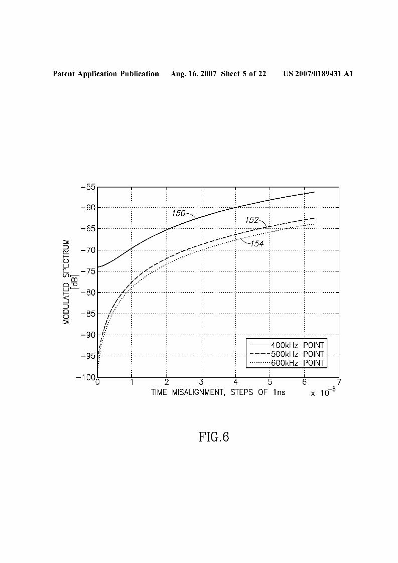
Patent Application Publication Aug. 16,2007 Sheet 5 of 22 US 2007/0189431 Al
-55 r----.--------,-------r---r----....--------,------,
-60 ••••••••••••••• l • • • • • • • • • • • • • • • • ••••••••••••• ~ ••••••••••••••• ; ••••••••••••••. .. 150 ::: : : 152 : _--;--
- 65 .... ... . ; : ~~'j'';~~::?::t; ;:-··_·····::::r::·~ .
: -- ····:··"--,54 : :-70 ............•·········>t:::;o.~.«,···················,··············., .
~~F~~·'··lrIiI/ ..,: : : : : :
~:: l"rJrTii/' . . . .,/ : : : : --400kHz POINT
-95 '/. : : : ; ----500kHz POINT .. : : : : ··········600kHz POINT· . . .· . . .· . . .
::::?!:::::>0:::fUWD... -75tf) r--1
m0-0wL..-Jf- -80::5::::>oo::::?!:
-1000=----"':-----=----=-----':-----=-----=-----::!7
x 10-8
FIG.6

Patent Application Publication Aug. 16,2007 Sheet 6 of 22 US 2007/0189431 Al
FREQUENCY
_. _. -PERFECT ALIGNMENT------6.4ns MIS-ALIGNMENT.........................
·················13.8ns MIS-ALIGNMENT- - -19.2ns MIS-ALIGNMENT--25.6ns MIS-ALIGNMENT
-20
O...--------.------r-----r-----r-------,r-------r------r-----r------.
-120
-1 400=-------';----=-------=---':------=---=-------=:----=-----'
~ -40::::>D::::IU
~ -60tn,.......,
OJ0-0wL......J~ -80::::>oo~ -100
FIG.7

Patent Application Publication Aug. 16,2007 Sheet 7 of 22 US 2007/0189431 Al
108-4 -2 0 2 4 6AM-PM DELAY [IN ns]
FIG.8
w<..9Z«:r:o
5.....-----------------------,4.5-+---------------------7'-------1
r---1 4-+---------------------,~----I
~L.....J 3.5-+----------------+-------1
3.......,..--------------+--------1
Z 2.5+----lI~-----------+--------I
2+---~----------+---------I
1.5+------A-----------d------____I
1+-----~,...,------------.r-----------I
0.5+------------"~-~-----------I
o+-...........,r""""""T~___r___r__~T"""""""I ......-r-___r___r___r__...........,r""""""T____r____r_~
-10 -8 -6
1086024DELAY [IN ns]
FIG.9
-4 -2AM-PM
zW<..9Z«:r:o
20.....-----------------------,18-ik----------------______,-----...
r---1 1 6 -+--------..I.---------------~-----Im~ 14-+------'Jk-----------~------I
12.........-------.--------~---------,.-...-.....10-+---Iot------~-----_____,---....,._....-____I8+--- --~----..y..._- f_\_--____I
6+----~,------------\~-----+---+--------I4+-----~ ___\_--+__......r_-----____I
2+----------I.........".~---------------------I0-+---T""""""T---r-___r__"'T""""""'1........_r"___r_....;::::~~___r____r__"'T""""""'1........_r"___r___r__.,........I
-10 -8 -6

16
14
r---1 12en""'0
L........J
0::: 10---lU
8«zw 6C)z 4«:r:u
2
0
Patent Application Publication Aug. 16,2007 Sheet 8 of 22 US 2007/0189431 Al
o 1 2 3 4 5AM FRACTION DELAY w.r.t AM INTEGER [IN ns]
FIG.10
0.5
0.4
~ 0.3L........J
~ 0.2w
z 0.1wC)
z 0«:r:u
-0.1
-0.2
.or. -
012 345AM FRACTION DELAY w.r.t AM INTEGER [IN ns]
FIG.11

Patent Application Publication Aug. 16,2007 Sheet 9 of 22 US 2007/0189431 Al
3.5r---1
~ 3L........J
z 2.5>w2
z1.5w
C) 1z«:r: 0.50
01 2 3 4 5 6 7 8 9 10
PM FRACTION DELAY w.r.t. PM INTEGER [IN ns]
FIG.12
40-.--------------------------.r---1
~ 35+------------------........-------L........J 190n::: 30d 25-+-------------::~-'------------::---===-----------I« 20-+-----~--------:::I...-==-------'<------------IZW 15+--~"L-----=:;;~----------------l
~ 10-+----+--....",.e;-------------------I;§ 5+---+r----------------------lo
O~.......,.----~-~-~____r-___r_-__r__-_r___~-___r_----l
o 1 2 3 4 5 6 7 8 9 10PM FRACTION DELAY w.r.t. PM INTEGER [IN ns]
FIG.13

Patent Application Publication Aug. 16,2007 Sheet 10 of 22 US 2007/0189431 Al
3o-.---------------------------,
f2,....., 25+------------:::,..c.----------..:::.......:",....----------lI N~~ 20+------:7'L--------------------'>.,o;r--------l
uZ ~ 15+-----+---------------------->,.------------l
L......J
W(...? w 10+----+-----------------------'<-------lz(f)«IO 5+---+---------------------=------JU Z
o+-'-'----:-1----r-~2=---r---:3=---.---4:-----1r--::5:----;r--::6:----r----=7:--T----=8----r----=-9----r~1:-::0:-i
PM FRACTION DELAY w.r.t. PM INTEGER [IN ns]
FIG.14
208~ P FLOPS
SIGNAL r" A,---~,,\
INPUTFF
212Q FLOPS /
,-------A r... SIGNALOUTPUTSAMPLE RATE
CONVERSION I----I~ FFBY
elk_hi/elk_lo
SIGNAL OUTPUT
D210
FFFF
FIG.15

Patent Application Publication Aug. 16,2007 Sheet 11 of 22 US 2007/0189431 Al
FF
412Q FLOPS /
,, ------A ~ SIGNALOUTPUT
SIGNAL OUTPUT
D410
SAMPLE RATEFF I----l-.l CONVERSION I----l-.l FF
BYelk_lo/elk_hi
FF
408~ P FLOPS
SIGNAL ~ A __.."
INPUT
FIG.16

""Cl~.....('D
=.....>'t:l
't:l-....(')
~.........0
=""Cl=0"-....(')
~.........0
=>=~....~Cl\
N0
'1 0:::::0 ......:J»("") rFJ--I =-0 ('D
('Dz - .....»z ....r~ N
G) 0
°1f"Tl....
--1:::::0 N:r: Nf"Tl:::::0
81 crFJN00......:J
---0....QO\0,j;o,.(.H....>....
NA
SDA
232
CKVDy. y=4 or 6 DIV240 CHAIN
IA
L+_+_+J 229227
I ICKVDz CKVDy
,------------------------,276 1 CLOCK CKVDz. z=16. 32.-----/! MODULE OR MORE DIV
236 1 238 CHAIN1
1
1
1 CKVDx1--1
: CKVDxa TDe''-' CKVDx. x=1 or 2 DIV: 242 CHAINL______________________ _~
225
226
228~r-..l..------,1 1
1 1
1 0 1 CKVDy CKVDxaAM-AM 1 fTl 1 IA+FA AMPLITUDE
PREDISTORTION ~ I CONTROL WORD(ACW)
.---,D-IG-IT-A-L-L-~---'; / ,
FA IMODUALATOR
7 i234 CKVDxa
CKVDz
, CKVDzI I
GAINNORMALIZATION
J224
A
/220
AMPLITUDEMODULATION
FIG.17A
r\~~A 1 PULSE CORDIC +~ SHAPING POLAR SIGNAL
FILTER PROCESSING
222 PHASE 223 AM-AMMODULATION PREDISTORTION
+PM-FM

~'t:l....(')
~.........o
=""Cl=0"....(')
~.........o
=
RFOUT
256
VARIABLECLOCK(CKV)
250--..L---
262
FIG.17B
264 266
CKVDy CKVDxOSCILLATORTUNING WORD(OTW)
.------------,DIGITAL 'f~
L-FF.,L.-IMODUALATOR
268 CKVDx
270
EXCEPTIONHANDLER
274
FREQUENCYCOMMAND
WORD (FCW)
FREF ADPLL IF+FFLOOP CKV
CKVDz CKVDy
272
/220

Patent Application Publication Aug. 16,2007 Sheet 14 of 22 US 2007/0189431 Al
SIGNALOUTPUT
286
284
000
282<l C)<l 0<l ---l
«'--- .-jz«
282
I'" '8 _I'" '8 -ISIGNALINPUT
TS ~ 40rv50ps
280/
285
AMux_etl(lo92 (m)-1 :0)
FIG.18

CrFJNoo~o....QO\0,j;o,.(.H....>....
~~....~Cl\
Noo......:J
rFJ
=('D('D.........Ul
o....NN
""Cl~.....('D
=.....~'t:l....(')
~.........o
=""Cl=0"....(')
~.........o
=
'l
~--I0_zlz»--1'rrlG)
°lrrl--1::::0:r:rrl::::0rrlo
c
NA
SDA
304302
,-------------------,I CLOCK CKVDz. z= 16. 32.----------,/! MODULE OR MORE DIV
308 ! 310 CHAIN
CKVDx. x=1 or 2 DIV314 CHAIN
299I I
CKVDz CKVDy
348
297
298
A
IA ENCODER ~ I I I
AND DEM G ;
CKVDy CKVDxAM-AM AMPLITUDE
PREDISTORTION CONTROL WORD(ACW)
Ir--D-IG-ITA-L-If:y,-I / I
FA IMODUALATOR} ~
CKVDz
, CKVDzI I
GAINNORMALIZATION
I296
/290
AMPLITUDEMODULATION
FIG.19A
PULSE CORDIC +SHAPING POLAR SIGNALFILTER PROCESSING
292 PHASE 294 AM-PMMODULATION PREDISTORTION
+PM --- FM
BBDATA-

FIG.19B
~'t:l....(')
~.........o
=""Cl=0"....(')
~.........o
=
RFOUT
c
322
CKVDy ---j--{)
'-7--....-------'
324CKVDx -----t>
338336
342
EXCEPTIONHANDLER
346
340
FREQUENCYCOMMAND
WORD (FCW)CKVDy CKVDx
FREF ADPLL IF +FF OSCILLATORLOOP CKV TUNING WORD
(OTW)CKVDz CKVDy DIGITAL "i../J.
MODUALATOR
344
/290

~'t:l....(')
~.........o
=""Cl=0"....(')
~.........o
=RF
OUT
436434
DCO GAINNORMALIZATION DCO
f R d[k] CKV" '\...J~:........j
Koco (OTW)
432
LOOPFILTER
RETIMED FREF
OSCILLATORPHASE
SAMPLER ACCUM.'--- R....:..:v['--=k]'--- Rv[i] L ~1",---_---,
444 442
DCO PERIODNORMALIZATION
426
CKR
446
CKR
:r:u
.---+-----1> TDC ~I-----+~
PHASEFILTER
FREF----+--1----1
422
DATA
REF.PHASE PHASE
CHANNEL ACCUM. DETECTORFREQUENCY + L RR[k] + ¢E[k]COMMAND + +(FCW) +_ 28
WORD (FCW) 424 ~----l430
448
420~
FIG.20

Patent Application Publication Aug. 16,2007 Sheet 18 of 22 US 2007/0189431 Al
i--------------------ly[k]
452 454FCW DT y'[k]
CKR CKR
L~~~~~-------------J
451
FREF
PHASE
458 460
CKR
470
450~
FIG.21
CKV/N,
464CKR
1--1I II II I
I466 I
II
I IL __ ~

Patent Application Publication Aug. 16,2007 Sheet 19 of 22 US 2007/0189431 Al
eJ>EPHASE
FREF
CKR/M, CKR
490
494!R CKR
DATA PATH KDCO~----~----------------------~
481FCW_CH ~ !R
512 KDCO x[k]
1-----------------------------1
482 484 488
FCW DT t y'[k]
496 498
CKR
508
500 ,--,I II II I
I506 I
II
I IL __ -.J
FIG.22

Patent Application Publication Aug. 16,2007 Sheet 20 of 22 US 2007/0189431 Al
x[i]
542
CKVDz CKVDy
536
524
,----------------------------------------------,III
Jy'[k]1
558CKV
560
564
CKVDz= CKV/z
562
CKVDy= CKV/y
554
CKR
FIG.23
566
PHASE
520~
FREF
DATA PATHL ~----------------------------------------~
521 y'[k](FM ONLY)
I
I fFCW_CH : Jy'[k] R:j+-
549 KDCO

CrFJNoo~o....QO\0,j;o.(.H....>....
~~....~Cl\
Noo......:J
rFJ
=('D('D.....N....o....NN
""Cl~.....('D
=.....~'t:l....(')
~.........o
=""Cl=0"....(')
~.........o
=DCa
378~ CKVDy
376I
CKVDx
366
ADPLL DIRECTPOINT INJECTION
+) d[k](OTW)
VARIABLE 380'-""PHASE ~ACCUM. ~0
I 1 U~(0
..'--'"
DCO GAINNORM.
SAMPLERRv[i]
386/ --r 384
CKR
Rv[k]
-.360
388T
DCO PERIODNORMALIZATION
394
FIG.24
RETIMED FREF (CKR)392
FREQ. FREQ. ERROR LOOP I 374DETECTOR ACCUM. FILTER
+\!!:[k] I ~ ~[k] I I
))----I..-.{+~ ~ .. L ~
-.368 ~ 370 J I BIT-~t:[k] I I~Rv[k] CKR 372 CKR SHIFT
390
365
:r:
I TDC ~I .. rI I> ::i
350~
354CKVDy p .. I ,
356 I I., i
CKVDx t-_ .. I358 ...
CKR----I>
FREF '" I
DATA FCW@ CKVDy

Patent Application Publication Aug. 16,2007 Sheet 22 of 22 US 2007/0189431 Al
12010080604020
x 109
1.242...--------r------r------r------r--------r------,1.241 . .
1.24
1.239
1.2381.237 ; ; ; ; .
. . . .. . . .1.236 ~ ~ > ~ ---: .
· . . . .· . . . .1.235
0
FIG.25A
12010080604020
x 1091.242...--------r------r------r------r--------r------,1.241 , .
1.24
1.239
1.2381.237 ; ; ; ; ; .
· . . . .· . . . .1.236 ~ ~ ~ ~ ~ .· . . . .· . . . .
1.2350
FIG.25B

US 2007/0189431 Al
DELAY ALIGNMENT IN A CLOSED LOOPTWO-POINT MODULATION ALL DIGITAL
PHASE LOCKED LOOP
REFERENCE TO PRIORITY APPLICATION
[0001] This application claims priority to u.s. ProvisionalApplication Ser. No. 601773,759, filed Feb. IS, 2006,entitled "Scheme To Achieve Precise Delay AlignmentBetween Amplitude And Phase/Frequency ModulationPaths In Digital Polar Transmitters And For Closed LoopTwo-Point Modulation At Different Injection Rates InADPLL", incorporated herein by reference in its entirety.
FIELD OF THE INVENTION
[0002] The present invention relates to the field of datacommunications and more particularly relates to an apparatus for and method of delay alignment in a closed looptwo-point modulation all digital phase locked loop (ADPLL).
BACKGROUND OF THE INVENTION
[0003] Modem complex envelope modulation schemessuch as Enhanced Data rates for GSM Evolution (EDGE),Wideband Code Division Multiple Access (WCDMA),Bluetooth Enhanced Data Rate (BT-EDR), Wireless LocalArea Network (WLAN), Worldwide Interoperability forMicrowave Access (WiMAX), etc. impose strict performance requirements on transceivers developed to supportthem, especially wireless handset transmitters. Stringentperformance requirements for many aspects of polar transmitters exist as well. A circuit diagram illustrating anexample prior art polar transmitter employing complexmodulation based on direct phase and amplitude modulationis shown in FIG. 1. The circuit, generally referenced 10,comprises a coder 12, I and Q TX filters 14, 16, polarcoordinate converter 18, local oscillator 20 and multiplier22.[0004] In operation, the bits bk to be transmitted are inputto the coder, which functions to generate I (real) and Q(imaginary) symbols therefrom according to the targetedcommunications standard. The I and Q symbols are pulseshaped and the resulting baseband signals are converted tophase (Ang{s(t)}), and magnitude (Mag{s(t)}) basebandsignals by the polar coordinate converter 18. The phase datais used to control the local oscillator 20 to generate theappropriate frequency signal, which is multiplied in multiplier/mixer 22 by the magnitude data resulting in the outputRF signal x(t). It is noted that this polar modulation schemeis better suited for digital implementation rather than analogimplementation.[0005] For digital polar transmitters, typical stringent performance requirements exist for modulated close-in andfar-out spectra, adjacent channel power ratio (ACPR), adjacent channel leakage ratio (ACLR), error vector magnitude(EVM), phase trajectory error (PTE) and percentage powerin-band. Implementation of such modern communicationstandards using the digital polar modulation approach ispossible only if precise alignment can be maintainedbetween the amplitude modulation (AM) and phase/frequency modulation (PM/FM) paths. This is an arduous taskas both amplitude and phase (or frequency) paths comprisedigital components that need to operate on coarser clockdomains (i.e. clocks with time period >10 ns) for power
1Aug. 16, 2007
efficiency, while complying with the stringent performancerequirements of modern wireless standards. In addition, thefront end circuit comprises digitally controlled analog components, such as the digitally controlled oscillator (DCO)(part of the local oscillator 20) and a digitally controlledpre-power amplifier (DPA) (part of the multiplier/mixer 22)which transforms the digital signals to the continuous-timedomain with high precision.[0006] In particular, for GSM/EDGE modulations theAM/PM alignment needs to be better than 10 nanoseconds,otherwise a degradation in the transmitter performanceoccurs. For WCDMA and the 4G modulations, however, theAM/PM alignment needs to be better than a nanosecond toprevent degradation in transmitter performance.[0007] Furthermore, direct two-point modulation in aclosed loop ADPLL requires modulation signals to be properly cancelled from the loop in order for the PLL to achieveoptimum phase noise performance. The phase modulationaccuracy requirement for modern wireless communicationstandards requires the direct point modulation to be at afaster rate than the reference signal typically used forreference point injection. Both these injection points need tobe precisely aligned to achieve desired ADPLL operation.[0008] The problem of time alignment described abovecan be generalized to any system wherein a signal is splitinto multiple independent paths and subsequently recombined again to reconstruct the original, but frequency translated, signal. Here to, implementation of such a system ispossible only if precise alignment can be maintainedbetween the independent signal paths. In order to producethe exact signal after all the independent paths are recombined, each and every signal path must have the exactamount of delay, otherwise the results will be distorted.[0009] Therefore, in general, there is a need for a mechanism capable of providing precise timing alignment for asignal that has been split into multiple independent paths. Inthe specific case of a polar transmitter, the mechanismshould be able to provide precise timing alignment for theAM and PM/FM modulation paths in a digital polar transmitter.
SUMMARY OF THE INVENTION
[0010] The present invention is a novel apparatus for andmethod of delay alignment in a closed loop two-pointmodulation all digital phase locked loop (ADPLL). Theinvention provides a fully digital delay alignment mechanism where better than nanosecond alignment is achieved byaccounting for processing delays in the various digitalcircuit modules of the transmitter and by the use of programmable delay elements spread across several clockdomains.[0011] Further, the invention provides a mechanism ofclock hand-off between different clock domains that preserves the existing alignment between the amplitude andphase/frequency modulation paths. In addition, the finaldigital stages ofboth AM and PM/FM paths share a commonclock domain source for the high speed clock used indelta-sigma modulators and integer/fraction delay matchingin each path. This enables clock domain alignment to beachieved between the two modulation paths.[0012] In addition, the propagation and settling delays invarious analog elements including DCO, dividers, quadswitch, buffers, level shifters and DPA are compensated forusing a tapped delay line (TDL). Each step in the tapped

US 2007/0189431 Al
delay line comprises a single buffer delay which can bedigitally controlled, thus enabling sub-nanosecond delayaligmnent between the two paths to be achieved.[0013] To ensure proper delay alignment is achieved, theinvention provides a signal correlative mechanism wherebydata from the two modulation paths to be matched is firstinterpolated and then cross-correlated to achieve accuracybetter than the clock domain of operation. In particular, highaccuracy is critical for the precise alignment ofreference anddirect point injection points in theADPLL. Due to the higherphase modulation accuracy requirement for a WCDMAtransmitter, the direct point injection operates on a highspeed clock while the reference point injection operates onthe retimed FREF clock rate (CKR), a much slower clock.The mechanism ofthe invention provides alignment ofthesetwo paths in the CKR (i.e. slow clock) domain. Further, theinterpolative correlation technique of the invention enablesthe precise tuning of high speed clock domain delays in thedirect point injection so as to achieve the overall necessaryaligmnent.[0014] The delay aligmnent scheme comprise fully digitalcontrols, which allow precise, predictable delay settings ofthe two modulation paths which are independent of anyprocess, voltage and temperature (PVT) variations. Furthermore, the mechanism provides for dynamic calibration of atapped delay line to account for any variation in the propagation delays in the analog front-end elements of the digitalpolar transmitter. A calibration mechanism is provided toachieve sub-clock period alignment within the direct and thereference point modulation injection within the ADPLL. Inaddition, the mechanism is dynamically adapted using anyavailable computing resource (either off or on-chip) such asa script processor in the case of the ADPLL embodimentpresented herein.[0015] The delay aligmnent mechanism of the invention isapplicable to any system in which a signal is split intomultiple independent paths and subsequently recombined toreconstruct the original signal. In order to produce the exactsignal after all the independent paths are recombined, thedelays of each and every individual signal path must match,otherwise the results will be distorted. Note that the invention is intended for use in a digital radio transmitter ortransceiver but can be used in other applications as well,such as a general communication channel and data converters.[0016] Note that many aspects of the invention describedherein may be constructed as software objects that areexecuted in embedded devices as firmware, software objectsthat are executed as part of a software application on eitheran embedded or non-embedded computer system running areal-time operating system such as WinCE, Symbian, OSE,Embedded LINUX, etc. or non-real time operating systemsuch as Windows, UNIX, LINUX, etc., or as soft corerealized HDL circuits embodied in an Application SpecificIntegrated Circuit (ASIC) or Field Programmable GateArray (FPGA), or as functionally equivalent discrete hardware components.[0017] There is thus provided in accordance with thepresent invention, a method of aligning two-point datamodulation injection in a digital phase locked loop (DPLL),the method comprising the steps of first utilizing a referenceclock domain for reference point injection of modulationdata into the loop, second utilizing a direct clock referenceclock domain for direct point injection of the modulation
2Aug. 16, 2007
data into the loop and aligning the reference clock domainwith and the direct clock domain in the reference clockdomain utilizing interpolative correlation to precisely tunedelay adjustments associated with the reference point injection and the direct point injection resulting in the alignmentof both the reference clock domain and the direct clockdomain.[0018] There is also provided in accordance with thepresent invention, an apparatus for delay aligmnent oftwo-point data modulation injection in an all-digital phaselocked loop (ADPLL) comprising direct injection meansadapted to inject modulation data samples into the loop at adata clock rate derived from a digital controlled oscillator(DCa) output clock, a digital delay adjustment moduleadapted to generate adjusted modulation data samples at anintermediate clock rate higher than and derived from thedata clock rate, a sample rate converter operative to generatereference modulation data samples at a reference clock ratefrom the adjusted modulation data samples, reference pointinjection means adapted to be clocked at the reference clockrate.[0019] There is further provided in accordance with thepresent invention, a apparatus for alignment of two-pointdata modulation injection in a digital phase locked loop(DPLL) comprising a reference clock domain for referencepoint injection of modulation data into the loop, a directclock reference clock domain for direct point injection ofthemodulation data into the loop and delay alignment means foraligning the reference clock domain with and the directclock domain in the reference clock domain utilizing interpolative correlation means to precisely tune delay adjustments associated with the reference point injection and thedirect point injection resulting in the alignment of both thereference clock domain and the direct clock domain.[0020] There is also provided in accordance with thepresent invention, a polar transmitter comprising means forsplitting transmit data into amplitude modulation data andphase modulation data, an amplitude modulation circuitoperative to generate an amplitude signal in accordance withthe amplitude modulation data, a frequency synthesizercomprising a digital phase locked loop (DPLL), the DPLLcomprising reference point modulation injection and a directpoint modulation injection and operative to generate acarrier signal in accordance with the phase modulation dataand means for utilizing different signal sampling rates for thereference point modulation injection and the direct pointmodulation injection.
BRIEF DESCRIPTION OF THE DRAWINGS
[0021] The invention is herein described, by way ofexample only, with reference to the accompanying drawings,wherein:[0022] FIG. 1 is a block diagram illustrating a prior artcomplex polar modulator with direct phase and amplitudemodulation;[0023] FIG. 2 is a block diagram illustrating a single chippolar transceiver radio incorporating an all-digital localoscillator based transmitter and receiver;[0024] FIG. 3 is a block diagram illustrating a single chippolar transmitter based on a DCa and digitally controlledpower amplifier (DPA) circuits;[0025] FIG. 4 is a diagram illustrating spectral replicas ofa modulating signal and associated filtering through a zeroorder hold;

US 2007/0189431 Al3
Aug. 16, 2007
DETAILED DESCRIPTION OF THEINVENTION
Notation Used Throughout
[0048] The following notation is used throughout thisdocument.
[0046] FIG. 25A is a graph illustrating the use of multirate correlation determined using analytic clock alignmentfor the alignment of direct and reference point injections;and[0047] FIG. 25B is a graph illustrating the use of multirate correlation determined using correlative measures totune multiple clock domain delays for the alignment ofdirect and reference point injections.
[0026] FIG. 5 is a block diagram illustrating the amplitudeand phase modulation paths of the polar transmitter;[0027] FIG. 6 is a graph illustrating the effect of misalignment between amplitude and phase on several points of theEDGE spectrum;[0028] FIG. 7 is a graph illustrating the effect of misalignment between amplitude and phase on the EDGE spectrumfor several different time mismatch delays;[0029] FIG. 8 is a graph illustrating the degradation inEVM for WCDMA as a function of time mismatch betweenamplitude and phase modulation paths;[0030] FIG. 9 is a graph illustrating the degradation inACLR for WCDMA as a function oftime mismatch betweenamplitude and phase modulation paths;[0031] FIG. 10 is a graph illustrating the degradation inACLR for WCDMA as a function oftime mismatch betweenamplitude integer and fractional bits;[0032] FIG. 11 is a graph illustrating the degradation inEVM for WCDMA as a function of time mismatch betweenamplitude integer and fractional bits;[0033] FIG. 12 is a graph illustrating the degradation inEVM for WCDMA as a function of time mismatch betweenphase integer and fractional bits;[0034] FIG. 13 is a graph illustrating the degradation inACLR for WCDMA as a function oftime mismatch betweenphase integer and fractional bits;[0035] FIG. 14 is a graph illustrating TX spectral noisecontribution degradation in the corresponding RX band forWCDMA as a function of time mismatch between phaseinteger and fractional bits;[0036] FIG. 15 is a block diagram illustrating a digitaldelay adjustment block in accordance with the presentinvention for a signal propagating from a slow clock domainto a fast clock domain;[0037] FIG. 16 is a block diagram illustrating a digitaldelay adjustment block in accordance with the presentinvention for a signal propagating from a fast clock domainto a slow clock domain;[0038] FIGS. 17Aand 17B are a block diagram illustratinga first embodiment of a WCDMA transmitter having precisedelay alignment between amplitude and frequency modulation paths;[0039] FIG. 18 is a block diagram illustrating a tappeddelay line in accordance with the present invention;[0040] FIGS. 19Aand 19B are a block diagram illustratinga second embodiment of a WCDMA transmitter havingprecise delay alignment between frequency and amplitudemodulation;[0041] FIG. 20 is a block diagram illustrating a firstgeneration ADPLL based DRP transmitter;[0042] FIG. 21 is a block diagram illustrating the phasemodulation path in a first generation ADPLL based DRPtransmitter;[0043] FIG. 22 is a block diagram illustrating the phasemodulation path in a second generation ADPLL based DRPtransmitter;[0044] FIG. 23 is a block diagram illustrating the phasemodulation path in a third generation ADPLL based DRPtransmitter;[0045] FIG. 24 is a block diagram illustrating an ADPLLwith direct point injection and reference point injection ratesof different clock domains;
Term
ACLRACPRACWADCADPLLARMASICBISTBT-EDRCICCKRCKVCMOSCORDICDBBDCODCXODDADEMDFCDPADPLLDRACDRPEDGEEVMFCWFMFPGAFREFGSMHBHDLIEEEIPMLBLDOLUTMOSOTFOT!OTWPAPARPLLPMPPAPSFPTEQAMRFRFBISTRMSSAWSoC
Definition
Adjacent Channel Leakage RatioAdjacent Channel Power RatioAmplitnde Control WordAnalog to Digital ConverterAll Digital Phase Locked LoopAdvanced RISC Machine (previously Acorn RISC Machine)Application Specific Integrated CircuitBuilt-In Self TestBluetooth Extended Data RateCascaded Integrator Comb FilterRetimed Reference ClockVariable Oscillator ClockComplementary Metal Oxide SemiconductorCOordinate Rotation DIgital ComputerDigital BasebandDigitally Controlled OscillatorDigitally Controlled Crystal OscillatorDigital Delay AdjustDynamic Element MatchingDigital Frequency ConversionDigital Power AmplifierDigital Phase Locked LoopDigital to RF Amplitnde ConversionDigital RF Processor or Digital Radio ProcessorEnhanced Data rates for GSM EvolutionError Vector MagnitndeFrequency Command WordFrequency ModulationField Progrannnable Gate ArrayFrequency ReferenceGlobal System for Mobile CommunicationsHigh BandHardware Description LanguageInstitnte of Electrical and Electronic EngineersIntegrated Power ManagementLow BandLow Drop OutLook-Up TableMetal Oxide SemiconductorOscillator Tuning FractionalOscillator Tuning IntegerOscillator Tuning WordPower AmplifierPeak-To-Average RatioPhase Locked LoopPhase ModulationPre-Power AmplifierPulse-Shaping FilterPhase Trajectory ErrorQuadratnre Amplitnde ModulationRadio FrequencyRF Built-In Self TestRoot Mean SquaredSurface Acoustic WaveSystem on Chip

US 2007/0189431 Al4
Aug. 16, 2007
[0049] The present invention is a novel apparatus for andmethod of delay alignment between amplitude and phase/frequency modulation paths in a digital polar transmitter.The invention provides a fully digital delay alignmentmechanism where better than nanosecond alignment isachieved by accounting for processing delays in the digitalcircuit modules of the transmitter and by the use of programmable delay elements spread across several clockdomains. Tapped delay lines compensate for propagationand settling delays in analog elements such as the DCO,dividers, quad switch, buffers, level shifters and digitalpre-power amplifier (DPA). A signal correlative mechanismis provided whereby data from the amplitude and phase/frequency modulation paths to be matched is first interpolated and then cross-correlated to achieve accuracy betterthan the clock domain of comparison. Within the ADPLLportion ofthe transmitter, precise alignment ofreference anddirect point injection points in the ADPLL is provided usingmultiple clock domains, tapped delay lines and clock adjustment circuits.[0050] The delay alignment mechanism of the invention isapplicable to any system in which a signal is split intomultiple independent paths and subsequently recombined toreconstruct the original signal. In order to produce the exactsignal after all the independent paths are recombined, thedelays of each and every individual signal path must match,otherwise the results will be distorted. Note that the invention is intended for use in a digital radio transmitter ortransceiver but can be used in other applications as well,such as a general communication channel and data converters.[0051] To aid in understanding the principles of thepresent invention, the description is provided in the contextof a digital RF processor (DRP) based transmitter that maybe adapted to comply with a particular wireless communications standard such as GSM, Bluetooth, EDGE, WCDMA,WLAN, WiMax, etc. It is appreciated, however, that theinvention is not limited to use with any particular communication standard and may be used in optical, wired andwireless applications. Further, the invention is not limited touse with a specific modulation scheme but is applicable toany modulation scheme including both digital and analogmodulations.[0052] Note that throughout this document, the term communications device is defined as any apparatus or mechanism adapted to transmit, receive or both transmit andreceive data through a medinm. The communications devicemay be adapted to communicate over any suitable mediumsuch as RF, wireless, infrared, optical, wired, microwave,
Term
SRAMSRCTDCTDLVCOWCDMAWiMAXWLAN
-continued
Definition
Static Read Only MemorySample Rate ConversionTime to Digital ConverterTapped Delay LineVoltage Controlled OscillatorWideband Code Division Multiple AccessWorld Interoperability for Microwave AccessWireless Local Area Network
DETAILED DESCRIPTION OF THEINVENTION
etc. In the case of wireless communications, the communications device may comprise an RF transmitter, RF receiver,RF transceiver or any combination thereof. The notationDRP is intended to denote either a Digital RF Processor orDigital Radio Processor. References to a Digital RF Processor infer a reference to a Digital Radio Processor and viceversa.[0053] A block diagram illustrating a single chip polartransceiver radio incorporating an all-digital local oscillatorbased transmitter and receiver is shown in FIG. 2. Forillustration purposes only, the transmitter, as shown, isadapted for the GSM/EDGE/WCDMA cellular standards. Itis appreciated, however, that one skilled in the communication arts can adapt the transmitter illustrated herein toother modulations and communication standards as wellwithout departing from the spirit and scope of the presentinvention.[0054] The radio, generally referenced 30, comprises ascript processor 60 adapted to execute the delay alignmentmechanism of the present invention (represented as taskblock 80), digital baseband (DBB) processor 62, memory 64(e.g., static RAM), TX block 42, RX block 58, crystal 38 anddigitally controlled crystal oscillator (DCXO) 50, front-endmodule 46 and antenna 44, power management unit 34, RFbuilt-in self test (BIST) 36, battery 78 and battery management circuit 32. The TX block comprises high speed and lowspeed digital logic block 40 including YAmodulators 52, 54,digitally controlled oscillator (DCO) 56 and digitally controlled power amplifier (DPA) 48. The RX block comprisesa low noise transconductance amplifier 66, current sampler68, discrete time processing block 70, analog to digitalconverter (ADC) 72 and digital logic block 74. Note thatalternatively, the delay alignment mechanism of the invention can be implemented using dedicated logic.[0055] The principles presented herein have been used todevelop three generations of a Digital RF Processor (DRP):single-chip Bluetooth, GSM and GSM/EDGE radios realized in 130 nm, 90 nm and 65 nm digital CMOS processtechnologies, respectively. The common architecture ishighlighted in FIG. 2 with features added specific to thecellular radio. The all digital phase locked loop (ADPLL)based transmitter employs a polar architecture with alldigital phase/frequency and amplitude modulation paths.The receiver employs a discrete-time architecture in whichthe RF signal is directly sampled and processed using analogand digital signal processing techniques.[0056] A key component is the digitally controlled oscillator (DCO) 56, which avoids any analog tuning controls. Adigitally-controlled crystal oscillator (DCXO) generates ahigh-quality base station-synchronized frequency referencesuch that the transmitted carrier frequencies and the receivedsymbol rates are accurate to within 0.1 ppm. Fine frequencyresolution is achieved through high-speed~!ldithering of itsvaractors. Digital logic built around the DCO realizes anall-digital PLL (ADPLL) that is used as a local oscillator forboth the transmitter and receiver. The polar transmitterarchitecture utilizes the wideband direct frequency modulation capability of the ADPLL and a digitally controlledpower amplifier (DPA) 48 for the amplitude modulation.The DPA operates in near-class-E mode and uses an array ofnMOS transistor switches to regulate the RF amplitude. It isfollowed by a matching network and an external front-endmodule 46, which comprises a power amplifier (PA), atransmit/receive switch for the common antenna 44 and RX

US 2007/0189431 Al Aug. 16, 20075
phase/frequency modulator 104 and DCa 106. The DRACcomprises an amplitude modulator 102 and digital poweramplifier (DPA) 108.
sgn(x)=1 for x~O;sgn(x)=-I for x<O;wo=2Jtfo is the angular RF carrier frequency;8[k] is the modulating baseband phase of the kth
(1)Ypzw(t)~sgn(cos(Ulot+8 fk])
RF Polar Transmitter in Deep-Submicron CMOS
[0062] A paradigm facing analog and RF designers ofdeep submicron CMOS circuits is that in a deep-submicronCMOS process, time-domain resolution of a digital signaledge transition is superior to voltage resolution of analogsignals. A successful design approach in this environmentwould be to exploit the paradigm by emphasizing (1) fastswitching characteristics or high fr (40 ps and 100 GHz inthis process, respectively) of MaS transistors: high-speedclocks and/or fine control of timing transitions; (2) highdensity of digital logic (e.g., 250 kgates/mm2 in 90 nmprocess) makes digital functions extremely inexpensive; and(3) small device geometries and precise device matchingmade possible by the fine lithography, while avoiding (1)biasing currents that are commonly used in analog designs;(2) reliance on voltage resolution; and (3) nonstandarddevices that are not needed for memory and digital circuits.[0063] FIG. 3 illustrates an application of the new paradigm to an RF wireless transmitter performing arbitraryquadrature amplitude modulation (QAM). The low cost ofdigital logic allows for the use of sophisticated digital signalprocessing techniques. The tiny and well matched devicesallow for precise and high-resolution conversions fromdigital to analog domains. The use of ultra high-speedclocks, i.e. high oversampling ratios, can eliminate the needfor subsequent dedicated reconstruction filtering of spectralreplicas and switching transients, so that only the naturalfiltering of an oscillator (lis due to the frequency-to-phaseconversion), matching network of power amplifier andantenna filter are relied upon.[0064] Since the converters utilize DCa clocks that are ofhigh spectral purity, the sampling jitter is very small. Thesampling jitter is not significantly affected by modulation,since the jitter due to modulation is not greater than theoscillator thermal jitter. The conversion functions presentedherein are phase/frequency and amplitude modulations of anRF carrier realized using digitally-controlled oscillator(DCa) and digitally-controlled power amplifier (DPA) circuits, respectively. They are digitally-intensive equivalentsof the conventional voltage-controlled oscillator (YCO) andpower amplifier driver circuits.[0065] Due to the fine feature size and high switchingspeed of modern CMOS technology, the respective digitalto-frequency conversion (DFC) and digital-to-RF-amplitudeconversion (DRAC) transfer functions can be made verylinear and of high dynamic range. The frequency deviationoutput signal is fed into the DCa-based Brbit DFC, whichproduces the phase modulated (PM) digital carrier:
where[0066][0067][0068][0069]sample;[0070] The phase 8(t)=J_=tf(t)dt is an integral of frequency deviation, where t=k-To with To being the samplingperiod represented in BF=IF+FF bits, IF and FF being integerand fractional bits respectively.
surface acoustic wave (SAW) filters. Fine amplitude resolution is achieved through high-speed ~!l dithering of theDPA nMOS transistors.
[0057] The receiver 58 employs a discrete-time architecture in which the RF signal is directly sampled at the Nyquistrate of the RF carrier and processed using analog and digitalsignal processing techniques. The transceiver is integratedwith a script processor 60, dedicated digital base bandprocessor 62 (i.e. ARM family processor) and SRAMmemory 64. The script processor handles various TX andRX calibration, compensation, sequencing and lower-ratedata path tasks and encapsulates the transceiver complexityin order to present a much simpler software programmingmodel.
[0058] The frequency reference (FREF) is generated onchip by a 26 MHz digitally controlled crystal oscillator(DCXO) 50. An integrated power management (PM) systemis connected to an external battery management circuit 32that conditions and stabilizes the supply voltage. The PMcomprises multiple low drop out (LDO) regulators thatprovide internal supply voltages and also isolate supplynoise between circuits, especially protecting the DCa. TheRF built-in self-test (RFBIST) 36 performs autonomousphase noise and modulation distortion testing as well asvarious loopback configurations for bit-error rate measurements. The transceiver is integrated with the digital baseband, SRAM memory in a complete system-on-chip (SoC)solution. Almost all the clocks on this SoC are derived fromand are synchronous to the RF oscillator clock. This helps toreduce susceptibility to the noise generated through clockingof the massive digital logic.
[0059] The transmitter comprises a polar architecture inwhich the amplitude and phase/frequency modulations areimplemented in separate paths. Transmitted symbols generated in the digital baseband (DBB) processor are firstpulse-shape filtered in the Cartesian coordinate system. Thefiltered in-phase (1) and quadrature (Q) samples are thenconverted through a CORDIC algorithm into amplitude andphase samples of the polar coordinate system. The phase isthen differentiated to obtain frequency deviation. The polarsignals are subsequently conditioned through signal processing to sufficiently increase the sampling rate in order toreduce the quantization noise density and lessen the effectsof the modulating spectrum replicas.
[0060] A more detailed description of the operation of theADPLL can be found in U.S. Patent Publication No. 2006/0033582AI, published Feb. 16, 2006, to Staszewski et aI.,entitled "Gain Calibration of a Digital Controlled Oscillator," U.S. Patent Publication No. 2006/00387IOAI, published Feb. 23, 2006, Staszewski et aI., entitled "HybridPolar/Cartesian Digital Modulator" and U.S. Pat. No. 6,809,598, to Staszewski et aI., entitled "Hybrid Of Predictive AndClosed-Loop Phase-Domain Digital PLL Architecture," allof which are incorporated herein by reference in theirentirety.
[0061] A block diagram illustrating a single chip polartransmitter based on a DCa and digitally controlled poweramplifier (DPA) circuits is shown in FIG. 3. The transmitter,generally referenced 90, comprises a digital signal processorblock 92, digital to frequency conversion (DFC) 98 anddigital to RF amplitude conversion (DRAC) 100. The DSPblock 92 comprises I1Q pulse shaping filtering 94 andCORDIC polar signal processing 96. The DFC comprises a

US 2007/0189431 Al
[0071] The amplitude modulation (AM) signal controlsthe envelope of the phase-modulated carrier by means of theDPA based BA-bit DRAC. Higher-order harmonics of thedigital carrier are filtered out by a matching network so thatthe sgn( ) operator is dropped. The composite DPA outputcontains the desired RF output spectrum.
YR(t)~afklcos(())ot+8fk]) (2)
where ark] is the modulating baseband amplitude of the k th
sample. The amplitude is represented in BA=IA+FA bits, IAand FA being integer and fractional bits respectively.[0072] Despite their commonalities there are importantdifferences between the two conversion functions. Due tothe narrowband nature of the communication system, theDFC operational dynamic range is small but with a fineresolution. On the contrary, the DRAC operating range, onthe other hand, is almost full scale, but not as precise. Inaddition, the phase modulating path features an additionallis filtering caused by the frequency-to-phase conversion ofthe oscillator. The signal processing and delay between theAM and PM paths must be matched, otherwise the recombined composite signal will be distorted. Matching invariability to the process, voltage and temperature (PVT)changes, however, is guaranteed by the clock-cycle accuratecharacteristics of digital circuits. The group delay of theDCO and DPA circuits is relatively small (e.g., tens ofpicoseconds due to the high frofthe deep-submicron CMOSdevices) in comparison with the tolerable range (tens ofnanoseconds).[0073] The DFC and DRAC are key functions of theall-digital transmitter that does not use any current biasing ordedicated analog continuous-time filtering in the signal path.In order to improve matching, linearity, switching noise andoperational speed, the operating conversion cells (i.e. bit tofrequency or RF carrier amplitude) are mainly realized asunit weighted. Due to the excellent device matching characteristics in a deep-submicron CMOS process, it is relatively easy to guarantee at least 7-bit conversion resolutionin one iteration cycle without resorting to elaborate layoutschemes. The DFC and DRAC architectures are presentedinfra.[0074] Spectral replicas of the discrete-time modulatingsignal appear at the DCO and DPA inputs at integer multiplies of the sampling rate frequency fs ' as shown in FIG. 4.They are attenuated through multiplication of the sinc2
function due to the zero-order hold of the DCO/DPA input.The frequency spectrum Sjw) replicas are further attenuatedby 6 dB/octave through the lis operation of the oscillator tofinally appear at the RF output phase spectrum S<j>(w). Thesampling rate fs is chosen to be high enough for the replicasto be sufficiently attenuated, thus making the RF signalundistinguishable from that created by the conventionaltransmitters with continuous-time filtering at baseband.
Amplitude and Phase Modulation
[0075] A block diagram illustrating the amplitude andphase modulation paths of an example polar transmitter isshown in FIG. 5. The polar transmitter, generally referenced110, comprises a pulse shaping filter 112 and CORDIC 114which splits the data into amplitude and phase modulationpaths. The amplitude modulation path comprises gain normalizer 116, AM-AM predistortion 118, amplitude interpolation 120, encoder and dynamic element matching (DEM)122, digital ~!l modulator 124 and digital power amplifier
6Aug. 16, 2007
(DPA) 144. The phase modulation path comprises AM-PMpredistortion (as well as conversion to frequency) 126, phaseinterpolation 128, ADPLL loop 130, encoder and DEM 132,digital ~!l modulator 134 and DCO 136.[0076] In accordance with the invention, the transmitteralso comprises a clock divider array comprising dividerchains 138, 140, 142. Clock divider chain 138 functions todivide the variable clock CKV output of the DCO by I or 2to generate CKVDx, where x=1 or 2. Clock divider chain140 functions to divide the CKVDx clock by 4 or 8 togenerate CKVDy, where y=4 or 8 (or 8 or 16, respectively,if x=2). Clock divider chain 142 functions to divide theCKVDy clock by 4 or 8 to generate CKVDz, where z=16,32 or higher.[0077] For the polar transmitter 110, the pulse-shapingfilter contains separate I and Q filters followed by aCORDIC algorithm to convert the I and Q data to polardomain phase and amplitude outputs. The pulse shapingsampling rate is typically derived from the reference clock(or the down-divided CKV clock, preferably through afractional-N division mauner), the output of the pulse shaping filter is then interpolated to smoothen both the amplitudeand phase modulating signals. The phase output of theCORDIC is adjusted for AM-PM distortions in the DPA andthe PA. It is then differentiated to fit the IF+FF bits FCWfrequency format after interpolation MF to the DCO directmodulation rate of the ADPLL input. During the modulationstage, the ADPLL drives the DCO varactors with NF bitsinteger bits and SDF bit ~!l dithered fractional bits.[0078] The amplitude output is scaled for the appropriatepower level as well as mapped to the step size ofthe digitallycontrolled power amplifier (DPA). The amplitude outputthen undergoes AM-AM predistortion followed by interpolation MA to the appropriate injection rate for the DPA. TheIA+FA bit amplitude control word (ACW) is then convertedto the NA-bit integer unit-weighted format of the DPA. Adedicated bank of DPA transistors also undergoes a highfrequency third-order~!l modulation to enhance the amplitude resolution (by SDA bits) and to achieve noise spectralshaping. Both the DCO and the DPA controllers also perform dynamic element matching (DEM) to enhance thetime-averaged linearity due to possible device mismatch.The above described polar mechanism is employed forcomplex modulation schemes such as EDGE, WCDMA andothers. In the GSM mode operation, however, a singleGaussian pulse shaping filter is used and the CORDICcircuit is bypassed. The AM path is temporarily engaged toramp the output power to a desired level and then remainsfixed throughout the payload.[0079] Critical to achieving satisfactory performance of apolar transmitter is proper delay matching between phaseand amplitude modulation signals from the CORDIC inputthrough to the DPA or PA output. Phase modulation isaccomplished by injecting the phase information to theADPLL, while the amplitude signal path is quite different asamplitude information is modified for power control andspectral replica mitigation. In order to reproduce the sourceI/Q data feeding the CORDIC at the antenna port, the delaysin the phase and amplitude paths of the transmitter must beproperly matched.
Alignment Accuracy Between Amplitude and PhaseModulation Paths
[0080] Beyond the CORDIC, both amplitude and phasemodulation paths comprise separate signal processing paths.

US 2007/0189431 Al
Desirable transmitter performance characteristics can beachieved only if the two distinct paths are properly tuned andaligned 'perfectly'. For complex modulation schemes thatutilize both of these modulation paths in a polar transmitter,mostly symmetric signal processing operations are done atlower clock rates to ensure that the alignment can bemaintained between the two paths. For high speed transmitter operations, however, the two paths may experiencemisalignment due to the need to perform asymmetric operations for accurate amplitude and phase reconstruction. Secondly, even for similar clock rates used in the two paths, theclock tree delays for each path are also independent and thusintroduce additional alignment skews. Thirdly, in the digitalto analog interfaces, both the amplitude and phase (orfrequency) modulation paths involve certain analog delays,which are a function of process, voltage and temperature(PVT).[0081] A confluence of several of these factors necessitatethat the alignment requirements for each modulation schemebe analyzed and appropriate design measures taken to ensurethat the optimal alignment accuracy is achieved. The timingalignment precision between amplitude and phase pathsrequired for 2.5G EDGE is in the order ofa few nanoseconds(i.e. <10 ns). While for WCDMA and 4G modulations, thisAM/PM alignment needs to be better than a nanosecond (i.e.<1 ns), otherwise severe degradation in critical transmitterperformance parameters occurs. A brief analysis of thealignment accuracy needed for EDGE and WCDMA modulations is presented below.
EDGE Modulation
[0082] Time alignment between amplitude and phase inthe case ofEDGE can be achieved in several stages. A coarsetime alignment block is placed after the CORDIC with aresolution of CKVD256 (i.e. CKV divided by 256) whereCKV is the channel frequency for high band (HB), and twicethe channel frequency for low band (LB). Finer time alignment blocks follow in the Cascaded Integrator Comb (CIC)interpolation block after each interpolator stage. This yieldsa progressively fine resolution down to CKVDy (CKVdivided by y) clock rate, which is the integer data injectionrate into the DCa and the DPA. Typically, this alignment isaccurate up to a few nanoseconds. Further alignment mechanisms are discussed infra.[0083] A graph illustrating the effect of misalignmentbetween amplitude and phase on several points of the EDGEspectrum is shown in FIG. 6. The graph shows the effects ofmisalignment at 400 kHz (solid trace referenced 150), 500kHz (dashed trace referenced 152) and 600 kHz (dotted tracereferenced 154) points on the close-in EDGE spectrum,averaged over 30 kHz around each point, with time delaybetween amplitude and phase swept from 0 to 60 ns.[0084] A graph illustrating the effect of misalignmentbetween amplitude and phase on the EDGE spectrum forseveral specific time mismatch delays is shown in FIG. 7.The graph shows several traces wherein trace 160 representsperfect alignment; trace 162 represents 6.4 ns misalignment;trace 164 represents 13.8 ns of misalignment, trace 166represents 19.2 ns of misalignment and trace 168 represents25.6 ns of misalignment.
WCDMA Modulation
[0085] For WCDMA, the CORDIC typically runs at a ratewhich is significantly higher than that of an EDGE TX. This
7Aug. 16, 2007
is required to preserve the much wider modulation signalbandwidth. This results in much higher frequency excursion(due to possible high speed 1800 phase transitions) as wellas faster amplitude changes due to a higher peak-to-averageratio (PAR) in WCDMA. This results in increased sensitivityofWCDMAmodulation reconstruction to the delay betweenthe amplitude and phase modulation paths. Simulated analysis results for WCDMA are presented hereinbelow.
[0086] A graph illustrating the degradation in error vectormagnitude (EVM) for WCDMA as a function of timemismatch between amplitude and phase modulation paths isshown in FIG. 8. The relative change in EVM expressed asa percentage versus the AM-PM delay in nanoseconds isplotted. It is noted that the degradation is not symmetricalfor negative and positive delays.
[0087] A graph illustrating the degradation in ACLR forWCDMAas a function oftime mismatch between amplitudeand phase modulation paths is shown in FIG. 9. The relativechange in ACLR expressed in dB versus the AM-PM delayin nanoseconds is plotted. The ACLR1 is represented astrace 172 while ACLR2 is represented as trace 170. Unlikethe impact in EVM performance, the impact on ACLRperformance is symmetrical for positive and negativedelays.
Alignment Accuracy Between Integer andFractional Bits of Phase and Amplitude
Modulations
[0088] The investigation results of the impact of integerand fractional alignment of amplitude and phase modulationpaths in a polar transmitter is now presented. SinceWCDMA is more sensitive to such artifacts, the resultspresented hereinbelow are based on WCDMA polar transmitter simulation results. These misalignments may be introduced by the fact that the integer part of each operates at theCKVDy clock rate (see FIG. 5), while the~!l modulators forthe fractional representation requires an over-sampling ratio(OSR) and hence uses a much higher rate clock CKVDx.
Alignment Requirement Between AmplitudeInteger/Fractional Bits
[0089] A graph illustrating the degradation in ACLR forWCDMAas a function oftime mismatch between amplitudeinteger and fractional bits is shown in FIG. 10. The relativechange in ACLR expressed in dB versus the AM fractionaldelay with respect to AM integer delay in nanoseconds isplotted. The ACLR1 is represented as trace 182 whileACLR2 is represented as trace 180.
[0090] A graph illustrating the degradation in EVM forWCDMAas a function oftime mismatch between amplitudeinteger and fractional bits is shown in FIG. 11. The relativechange in EVM expressed as a percentage versus the AMfractional delay with respect to AM integer delay in nanoseconds is plotted.
[0091] It is observed that the amplitude integer and fractional bit misalignment causes spectral re-growth whichresults in a degradation of the adjacent channel leakage, asshown in FIG. 10. As shown in FIG. 11, however, WCDMATX EVM is not very sensitive to the amplitude integer/fraction timing mismatch. The ACLR degradation indicates

US 2007/0189431 Al
that the nanosecond alignment accuracy is needed for goodtransmitter performance parameters.
Alignment Requirement Between PhaseInteger/Fractional Bits
[0092] A graph illustrating the degradation in EVM forWCDMA as a function of time mismatch between phaseinteger and fractional bits is shown in FIG. 12. The relativechange in EVM expressed as a percentage versus the PMfractional delay with respect to PM integer delay in nanoseconds is plotted.[0093] A graph illustrating the degradation in ACLR forWCDMA as a function of time mismatch between phaseinteger and fractional bits is shown in FIG. 13. The relativechange in ACLR expressed in dB versus the PM fractionaldelay with respect to PM integer delay in nanoseconds isplotted. The ACLRI is represented as trace 192 whileACLR2 is represented as trace 190.
[0094] A graph illustrating TX spectral noise degradationin the corresponding RX band for WCDMA as a function oftime mismatch between phase integer and fractional bits isshown in FIG. 14. The change in TX contributed noise in RXband expressed in dBc/Hz versus the PM fractional delaywith respect to PM integer delay in nanoseconds is plotted.
[0095] It is observed that WCDMA transmitter performance is quite sensitive to the integer/fraction timing mismatch. Such a misalignment has a direct impact on themodulated phase noise of the DCO. This severely degradesthe WCDMA spectrum. The impact on EVM, ACLR(s) andTX-to-RX noise is as shown in FIGS. 12, 13 and 14,respectively. The sharp degradation in the ACLR(s) and TXnoise contribution in the RX band warrants that a precisetime alignment for the phase integer and fractional bits isrequired for proper WCDMA transmit operation.
Mechanism to Achieve Sub-Nanosecond Amplitudeand Phase Modulation Path Alignment
[0096] The delay alignment mechanism ofthe invention ofachieving sub-nanosecond time alignment between theamplitude and phase modulation paths in a polar transmitterfor 2G/2.5G/3G and beyond will now be described in moredetail. It is appreciate that the mechanism described hereinbelow is applicable to any signal that has been split intomultiple independent paths and subsequently recombinedagain to reconstruct the original signal. In order to reproducethe exact signal when all the independent paths are recombined, each and every signal path needs to be delay aligned(i.e. each path must have the same exact amount of delaybefore recombination), otherwise the end results are likely tobe distorted.
[0097] The mechanism comprises both circuit construction elements and a calibration procedure to achieve thedesired goal of sub-nanosecond delay. In contrast to analogcentric approaches applicable to conventional analog I1Qtransmitters, where the processing delay per element isrelatively small but the delay alignment varies significantlyover process, voltage and temperature, for DRP based transmitters as presented herein, the delay alignment mechanismof the invention provides fully-digital control with preciselyknown and predictable delay settings of amplitude andphase/frequency modulation paths. Furthermore, the mecha-
8Aug. 16, 2007
nism is amenable to dynamic calibration using either a scriptprocessor 60 (FIG. 2) or any other on or off-chip computational resource.[0098] Using the mechanism of the invention, better thana nanosecond alignment accuracy is achieved by accountingfor processing delays in different digital modules and by theaddition of programmable delay elements across severalclock domains, namely CKVDz, CKVDy, CKVDx, andCKR (retimed reference), as described in more detail infra.Furthermore, the mechanism insures clock hand-offsbetween different clock domains preserve the existing alignment between the amplitude and phase/frequency modulation paths.
Multiple Clock Domain Delay Alignment Scheme
[0099] A block diagram illustrating a digital delay adjustment block in accordance with the present invention for asignal propagating from a slow clock domain to a fast clockdomain is shown in FIG. 15. The digital delay adjustmentblock, generally referenced 200, comprises a delay 202clocked by a low (slow) clock signal clk_lo adapted toreceive the input signal, sample rate converter 204 and delay206 clocked by a high (fast) clock signal clk_hi. Theequivalent circuit is shown below the double arrow andcomprises a plurality of P flip-flops 208 clocked by the slowclock clk_lo, sample rate conversion (SRC) 210 (i.e. interpolator) adapted to perform interpolation and convert fromthe high (fast) clock domain to the low (slow) clock domainand a plurality of Q flip-flops 212 clocked by the fast clockclk_hi.[0100] The digital delay adjustment block 200 enables theuse of two different clock domains in controlling the delayin a signal path. Note that these two clocks mayor may notbe derived from a single master clock source.[0101] A block diagram illustrating a digital delay adjustment block in accordance with the present invention for asignal propagating from a fast clock domain to a slow clockdomain is shown in FIG. 16. The digital delay adjustmentblock, generally referenced 400, comprises a delay 402clocked by a high (fast) clock signal clk_hi adapted toreceive the input signal, sample rate converter 404 (i.e.interpolator) and delay 406 clocked by a low (slow) clocksignal clk_lo. The equivalent circuit is shown below thedouble arrow and comprises a plurality of P flip-flops 408clocked by the fast clock clk_hi, sample rate converter(SRC) 410 adapted to convert from the low (slow) clockdomain to the high (fast) clock domain and a plurality of Qflip-flops 412 clocked by the slow clock clk_lo.[0102] The sample rate conversion technique usedbetween the flops placed in the two clock domains can bechosen as per the spectral and signal integrity needs of thesignal path. SRC may use simple zero-order hold, linear orsecond order interpolation or third order Lagrange (or cubicspline) interpolation/decimation schemes as needed. However note that in case the clk_hi and clk_lo clocks arecompletely asynchronous to each other, the accuracy ofsample rate conversion will be a limited by the accuracywith which the phase and edge timing relationships betweenthe two clock domains can be determined.[0103] A block diagram illustrating a first embodiment ofa WCDMA transmitter having precise delay alignmentbetween amplitude and frequency modulation paths isshown in FIGS. 17A and 17B. The transmitter, generallyreferenced 220, comprises a pulse shaping filter 222,

US 2007/0189431 Al Aug. 16, 20079
TABLE I
High Speed Clock Alignment Using Buffer Delays
[0114] In order to adjust the phase relationship betweenthe highest speed clocks used in each path, a set of bufferdelays are used to achieve very fine adjustment in picoseconds. A block diagram illustrating a tapped delay line inaccordance with the present invention is shown in FIG. 18.The tapped delay line (TDL), generally referenced 280,
output of the CORDIC is split using an exception handlingblock between the ADPLL and the quad-switch path. Theexception handler functions to compute the delta phase inthe CKVDz domain and then split it between the quadswitch and ADPLL in accordance with Table I presentedbelow. The Quad Out in the table below is the control for thequad-switch, while the Phase Out is the phase modulationthat is fed to the ADPLL as frequency modulation (FM).
[0109] For the polar transmitter incorporating exceptionhandling as in FIG. 17, modulation accuracy for complexwide modulation bandwidth standards such as WCDMA,BT-EDR, 4G, etc., in terms of EVM, ACLRs and far-outnoise, etc. is achieved by providing precise delay alignmentbetween (I) the phase modulation path in ADPLL, (2) theswitching control of quadrature modulated DCa phases and(3) the amplitude path. Note that the signal processingperformed on the amplitude and phase modulation paths isasymmetric and the digital delay adjust blocks are thereforetuned to achieve the requisite delay alignment between allthe modulation paths by accounting for the digital groupdelay of each digital signal processing block within eachpath.[0110] Furthermore, very precise nanosecond range delayis achieved by ensuring that for both the amplitude andphase, integer and fraction components are aligned in thehigh-speed CKVDx clock domain. For example, considerthe CKVDx clock is chosen to be the CKVD2 clock (approximately I GHz). In this case, the delay alignmentaccuracy between these different paths is less than I ns. Toensure such tight compliance, the mechanism of the invention provides the following:[0111] First, CKVDx based registers 232, 266 are introduced as the clock domain for the final stage of registers oninteger components of the AM and PM signals, respectively,which are otherwise handled in the CKVDy clock domain.[0112] Second, the CKVDx clock used for this final set ofregisters can precisely be the same clock used for both AMand PM/FM paths. This mitigates the effects of possibleindependent clock tree delays in AM and PM/FM paths.[0113] Third, alternately, the CKVDx clock used foramplitude and phase quad-switch paths; i.e. CKVDxa andCKVDxq, respectively; are adjusted for the physical analogdelay in the DCa and divider tree and DPA, respectively, asdescribed in more detail infra.
Phase Out Pout
Pin - 90 degPin - 180 degPin + 90 degPin
Qout(prev) + 1Qout(prev) + 2Qout(prev) - 1Qout(prev)
Quad Out Qout90 Deg ~ 1 Quadrant
TX Exception Handling Scheme
+45 to +135+135 to +225
-45 to -135-45 to +45
Delta Phase Pin
CORDIC and polar signal processing 223 which splits thedata into amplitude and phase modulation paths. The amplitude modulation path comprises gain normalizer 224, AMAM predistortion 226, digital delay adjustment 228, encoderand dynamic element matching (DEM) 230, digital ~!l
modulator 234 and digital power amplifier (DPA) 256. Thephase modulation path comprises AM-PM predistortion 276,phase interpolation 274, exception handler 272, ADPLLloop 270, encoder and DEM 264, digital ~!l modulator 268,DCa 262, quad switch 258, digital delay adjustment 246and quad sync 254.[0104] In accordance with the invention, the transmitteralso comprises a clock divider array comprising dividerchains 238, 240, 242. Clock divider chain 242 functions todivide the variable clock CKV output of the DCa by I or 2to generate CKVDx, where x=1 or 2. Clock divider chain240 functions to divide the CKVDx clock by 4 or 8 togenerate CKVDy, where y=4 or 8. Clock divider chain 238flillctions to divide the CKVDy clock by 4 or 8 to generateCKVDz, where z=16, 32 or higher. Tapped delay line (TDL)244 (TDLl) delays CKVDx by a programmable amount toyield CKVDxq. Similarly, tapped delay line (TDL) 245(TDL) delays CKVDx by a programmable amount to yieldCKVDxa.[0105] The WCDMA transmitter 220 provides precisedelay alignment between frequency and amplitude modulation (both integer and fractional components) as well as forthe quad switch based exception handling mechanism. Boththe amplitude modulation path and the quad switch utilizethe output of the tapped delay lines (TDL and TDLl)generated from the high speed clocks.[0106] In this example embodiment, the digital delayadjustment blocks 228, 246 are both modeled after the delayadjustment block of FIG. 15. In both cases, the two clocksused for clk_Io and clk_hi are CKVDz and CKVDy, respectively. With reference to FIGS. 5 and 17, since these twoclocks are derived from the same source (RF CKV clock inthis case), the possibility of signal degradation due toestimation of the timing relationship between clocks issimplified. Furthermore, specific to a polar transmitter, theclock rate typically increases from the baseband I/Q input tothe transmitter to the high-speed RF clock rate recombination of amplitude and phase. Therefore, as an example, inthis case the circuit of FIG. 15 is utilized wherein the SRCis represented by a linear interpolation of the data rate fromCKVDz to CKVDy clock domain.[0107] The scheme described supra is used as an alignment and data handoffbuilding block in FIG. 17 to create afully digital delay alignment scheme. This digital delayadjustment block comprises a precisely known and predictable delay setting based on (I) the two clock rates chosen asCKVDz and CKVDy, (2) the number of flip-flops (FFs)employed in each clock domain and (3) the linear interpolation (sample rate conversion) scheme chosen for the datahandoff.[0108] FIG. 17 illustrates the block diagram of a WCDMAcompliant polar transmitter using the hybrid polar/Cartesiantransmit modulator, described in detail in U.S. Patent Publication No. 2006/003871OAI, cited supra. This hybridarchitecture restricts the amount of phase modulation performed by the ADPLL to be less than ±45°. The sharperphase modulation transitions are handled by switchingbetween the four quadrature phases out of the DCa. In thetransmitter architecture of FIG. 17, the phase modulation

US 2007/0189431 Al
comprises a plurality of m buffers 282, each having a bufferdelay of'tB (40 to 50 ps in this example), followed by ananalog multiplexer 284 which is digitally controlled usingthe AMUX_CTL 285 digital (memory) register. The bufferBo 286 is a fixed buffer which is operative to ensure that theTDL delay is not skewed due to excessive loading on theswitchable buffers. The number ofbuffers effectively placedin the TDL is selected by setting the digital control wordAMUX_CTL to the appropriate value.[0115] For the polar transmitter incorporating an exception handling mechanism, a TDL, such as shown in FIG. 18,is used to compensate for the analog propagation andsettling delays in DCO, dividers, quad switch, buffers, levelshifters and DPA circuits. Each step in the tapped delay linecomprises a single buffer delay which is digitally controlled.This permits finer than CKV (i.e. sub-nanosecond) delayaligmnent between the all the constituent modulation paths.[0116] The circuit of FIG. 17 shows one example embodiment in which separate TDLs are introduced for the adjustment of the analog delay between the CKVDx clock used forthe ADPLL amplitude fractional modulation (i.e. CKVDxa)and the CKVDx clock used for amplitude and phase quadswitch paths, i.e. CKVDxq. The adjustment betweenCKVDx and CKVDxq functions to compensate for theanalog propagation delay in the DCO due to the Qof the LCtank, which determines the propagation delay once additional varactors are either switched in or removed from thetank. The DCO clock is followed by a plurality of clockdividers to divide the DCO clock running on a multiple ofthe channel frequency down to the High Band (HB) or LowBand (LB, where LB=HB/2) clock rate. These clock dividers have a response time which depends on their topology,the threshold set by the circuit biasing etc.[0117] Note that both the delays described above arefnnctions of process, voltage and temperature (PVT). Consequently, the adjustment in CKVDxa is made to maximizethe power added efficiency in the DPA. This is achieved byensuring that the DCO phase modulated clock fed to theDPA is correctly aligned to the amplitude modulation datafed to the DPA, which controls the number of devicesenabled in the DPA. The operation of a digital RF toamplitude converter suitable for use with the present invention is described in more detail in U.S. Patent PublicationNo. US2005/0287967, published Dec. 29, 2005, to Hung eta!., entitled "Low Noise High Isolation Transmit Buffer GainControl Mechanism," incorporated herein by reference in itsentirety.[0118] As described supra, one or more TDLs are used toacconnt for mostly analog propagation delays, which are afnnction of PVT and frequency. Optionally, a calibrationscheme incorporating a memory look-up table (LUT) is usedto adjust the TDL delays based on the on-chip temperatureand voltage monitors.[0119] A block diagram illustrating a second embodimentof a WCDMA transmitter having precise delay alignmentbetween amplitude and frequency modulation paths isshown in FIGS. 19A and 19B. The transmitter, generallyreferenced 290, comprises a pulse shaping filter 292,CORDIC and polar signal processing 294 which splits thedata into amplitude and phase modulation paths. The amplitude modulation path comprises gain normalizer 296, AMAM predistortion 298, digital delay adjustment 300, encoderand dynamic element matching (DEM) 302, digital ~!l
modulator 306 and digital power amplifier (DPA) 316. The
10Aug. 16, 2007
phase modulation path comprises AM-PM predistortion 348,phase interpolation 346, exception handler 344, ADPLLloop 342, encoder and DEM 336, digital ~!l modulator 340,DCO 334, quad switch 332 comprising TDL 328, digitaldelay adjustment 318 and quad sync 326.[0120] In accordance with the invention, the transmitteralso comprises a clock divider array comprising dividerchains 314, 312, 310. Clock divider chain 314 functions todivide the variable clock CKV output of the DCO by I or 2to generate CKVDx, where x=1 or 2. Clock divider chain312 functions to divide the CKVDx clock by 4 or 8 togenerate CKVDy, where y=4 or 8. Clock divider chain 310functions to divide the CKVDy clock by 4 or 8 to generateCKVDz, where z=16, 32 or higher.[0121] In this second embodiment, the TDL 328 is placedbetween the DCO 334 and the DPA 316. It is assumed thatthe analog propagation delay between the ADPLL modulation and the quad-switch is negligible. The purpose of theTDL in this scheme is to mainly maximize the PAE in theDPA.
Precise Aligmnent of Multi-Rate Direct andReference Point Data Modulation Injection in
ADPLL
[0122] The all-digital phase-locked loop (ADPLL) of thedigital radio-frequency processor (DRP) is described supraand in the references cited. The stringent modulation maskand spectral compliance requirements of 2.5G (EDGE)/3G(WCDMA) and beyond impose requirements that dictate theCORDIC rate in a polar transmitter. Further, in order tominimize the spectral re-growth due to the spectral replicas,the modulation injection occurs at a significantly higher rateas compared to the reference frequency clock used for thePLL. Running the ADPLL at a rate higher than the referenceclock rate, however, is wasteful as the variable phase/frequency feedback happens at the rate of retimed referenceor CKR. Both these modulation injection points must wellaligned for desired ADPLL operation. To better understandthe evolution oftheADPLL architecture to support the widerbandwidth phase/frequency modulation injection into theADPLL below, three generations of ADPLL are describedwith respect to the modulation path.[0123] In the ADPLL, the frequency reference (FREF)clock contains the only reference timing information for theRF frequency synthesizer to which phase and frequency ofthe RF output are to be synchronized. The RF variableoutput frequency fv is related to the reference frequency fR
according to the following formula.
(3)
where, N..FCW is real valued. The FREF source has excellent long term accuracy and stability, as compared to thevariable RF oscillator.[0124] A DRP transmitter based on an all-digital PLL(ADPLL) with a wideband frequency modulation capabilityis shown in FIG. 20. TheADPLL, generally referenced 420,comprises complex pulse shaping filter 422, digital prepower amplifier 438, adders 424, 432, phase detector 428,reference phase accumulator 426, loop filter 430, DCO gainnormalizer 434, DCO 436, variable phase accnmulator 440,sampler 442, FREF retimer 448, TDC 446 and TDC DCOperiod normalizer 444.[0125] The digitally-controlled oscillator (DCO) 436 produces a digital clock CKV in the RF frequency band. In the
US 2007/0189431 Al
feedforward path, the CKV clock toggles an NMas transistor switch of the near class-E RF digital power amplifier(DPA) 438 that is followed by a matching network (MN),and then terminated with a front-end module (FEM). In thefeedback path, the CKV clock is used to retime the FREFclock. The FREF retiming quantization error is determinedby the time-to-digital converter (TDC) 446, which is constructed as an array of inverter delay elements and registers,in order to compensate the quantization error by the system.The above operation strips FREF of its critical timinginformation and produces a retimed clock CKR that issubsequently used throughout the system. The CKR edgetimestamps are now synchronous to the RF oscillator, inwhich time separation between the closest CKR and CKVedges is time invariant. In this embodiment, it is beneficialto avoid injection pulling, whereby the slowly varyingtiming separation between CKR and CKV causes the oscillator to be pulled, thus creating a frequency beating eventthat exhibits itself as spurs in the generated output.
First Generation DRP Phase Modulation
[0126] A block diagram illustrating the phase modulationpath in a first generation ADPLL based DRP transmitter isshown in FIG. 21. The circuit, generally referenced 450,highlights the phase/frequency modulation path in the firstgeneration DRP of FIG. 20, which targets the Bluetoothwireless standard for short-range wireless communications.In order to ease timing in actual interfaces between theFREF, CKR and CKVD clock domains, the FREF clockretiming circuitry further performs retiming by the CKV/N1
clock, where typically N1=8.[0127] The circuit 450 illustrates the baseband transmitdata path 451 (comprising registers 452, 454 and whereinFCW_DT is the modulation data frequency command word)and the ADPLL loop, comprising phase accumulator/detector 456, adder 458, gain normalization 460, registers 470,468, 462, clock divider 466 and Dca 464.[0128] The circuit 450 highlights the phase/frequencymodulation path in the first embodiment DRP of FIG. 20. Inorder to ease timing in actual interfaces between the FREF,CKR and CKVD clock domains, the FREF clock retimingcircuitry further performs retiming by the CKV/N1 clock,where N1=8 is implemented.[0129] Several key features of the architecture include thefollowing. First, the ADPLL phase operation and the entirePM modulation are performed on the CKR clock. Second,the phase error samples <PE and the FCW-normalized modulating data samples y[k] of the feed-forward branch aremerged before the tuning word computation. Third, to theextent of the Dca support ofhigh frequency deviations andcorrect Dca gain estimation, KDCO' the modulating pathbandwidth is flat from DC to fR /2. Fourth, the Dca gainmultiplier, fR/KDco, controls both the modulation index~=2'Mp;Ts and the PLL bandwidth. For GSM, m=O.5 andK
DCOmust be estimated precisely.
Second Generation DRP Phase Modulation
[0130] A block diagram illustrating the phase/frequencymodulation path in a second generation ADPLL based DRPtransmitter which targets the GSM standard is shown in FIG.22. The circuit 480 illustrates the baseband data or modulation path 481 and ADPLL loop. The modulation pathcomprises source output register 482, delay registers 486,
11Aug. 16, 2007
488, 492, re-sampler or rate change converter 484 and gainnormalizer 490 wherein FCW_DT is the modulation datafrequency command word. The ADPLL loop comprisesphase accumulator/detector system 496, gain normalization498, adder 500, register 502, retiming registers 510, 508,clock edge divider 506 and Dca 504. This Figure illustratesthe phase/frequency modulation path in the second generation DRP (i.e. second embodiment), which targets the GSMstandard. In the GSM standard, the output of the pulseshaping filter is proportional to the frequency deviation andno conversion to the phase-proportional signal is explicitlyrequired.[0131] Several key features of the architecture of thesecond embodiment as described below. First, the ADPLLphase operation and the PM modulation are performed onthe CKR clock. In order to reduce circuit complexity andsave dissipated power, the pulse-shaping filter at the frontend of the modulating path can operate at a lower CKR/M1
rate, where M 1 is an integer, followed by the CKR-rateupsampler.[0132] Second, the tuning word samples and the Dcanormalized modulating data samples x[k] of the feed-forward branch are merged before the final CKR-clockedflip-flop 502 of the Dca interface.[0133] Third, to the extent of the Dca support of highfrequency deviations and correct Dca gain estimation,KDCO' the modulating path bandwidth is flat from DC tofR /2.[0134] Fourth, the Dca gain multiplier, fR/KDco nowappears independently in two places. anly the modulatingpath multiplier fR/KDco, which controls the modulationindex, is required to be configured precisely. The ADPLLloop multiplier needs only to be accurate to the extent of thedesired accuracy of the PLL bandwidth.
Third Generation DRP Phase Modulation
[0135] A block diagram illustrating the phase/frequencymodulation path in a third generation ADPLL based DRPtransmitter is shown in FIG. 23. The baseband multi-datarate data path 521 comprises adder 530, delay registers 546,522, 524, 526, 528, 536, 540, re-sampler or data rateconverter 542 and multiplier 534 and gain normalization 538for full bit multiplying the data by a high precision modulation path multiplier 544. The ADPLL loop 520 comprisesphase accumulator/detector system 548, loop gain normalization 550 for multiplying a low precision loop multiplier549, adder 554, registers 552, 556, clock edge dividers 560,562, 564, frequency reference re-sampling registers 568,566 and Dca 558.[0136] The Figure illustrates the phase/frequency modulation path in the third generation DRP (i.e. third embodiment). It adds support for the high data rates of the WCDMAand WLAN standards by dramatically increasing the frequency modulating bandwidth. The maximum bandwidthlimitation offR /2 in DRPI and DRP2 architectures is brokenhere by employing CKV-down-divided clocks in the finalstages of the modulating path. Since the modulating samplerate is much higher now than the CKR clock, the modulatingstream is merged with the ADPLL phase/frequency corrections just before the Dca input.[0137] The key features of the architecture are describedbelow. First, theADPLL phase operation is performed on theCKR clock. Second, in order to reduce circuit complexityand save dissipated power, the pulse-shaping filter at the
US 2007/0189431 Al12
Aug. 16, 2007
where An and Bn are two stationary random signal processesof vector length N. A maximum of the cross-correlation
DPA as well as feeds it back into the ADPLL loop. Cancellation of the modulated feedback is required in order toavoid the PLL loop from responding to the transient modulation effects. Without the reference feed cancellation, thePLL loop would not be sufficiently stable to meet therequired phase noise performance. In the absence of propermodulation cancellation, the computed frequency error canhave large spikes which can cause the ADPLL loop tochatter. Proper delay matching is thus a requisite for propertwo-point closed loop modulation without degradation ofthe ADPLL phase domain performance. Thus, the ADPLLloop maintains the proper center frequency by exact cancellation of two modulation injections to the loop.[0143] Reference point modulation injection in the closedloop PLL takes place at the phase frequency detector 368 atthe CKR rate, where the difference between reference frequency control word (FCW) and the feedback frequencydata (obtained by the differentiation of variable clock phasewith respect to FREF) is computed. While the direct modulation signal is fed back through the ADPLL feedback loop(which comprises accumulator 384 and time-to-digital converter (TDC) 390) with some propagation delay, the reference FCW signal that carries the same modulation information in the CKR clock domain must be properly aligned intime in order to yield zero phase/frequency error. Note theDCO interface block receives the fixed point oscillatortuning word (OTW) with the integer and fractional portionssplit between OTI 378 and OTF 380 blocks, respectively.The OTI operates on the CKVDy clock while the OTFcomprises a sigma-delta modulator that operates on the highspeed CKVDx clock. Note that the OTI and OTF blockscomprise the same frequency modulation integer and fraction blocks as shown in FIGS. 17 and 19.[0144] In accordance with the invention, the requiredalignment is achieved in two stages: one being the result ofmathematical and digital analysis which provides a startingpoint for delay matching and the second being performingmathematical correlation between the reference and feedback signals so as to provide quantitative results on themagnitude of the delay mismatch. The first step results inobtaining a register level manual delay alignment whichbrings the signals into coarse delay alignment.[0145] To ensure proper delay alignment is achieved, themechanism of the invention comprises signal correlativemeasures wherein data from the two paths to be matched isfirst interpolated and then cross-correlated to achieve accuracy better than the clock domain of comparison. In particular, this is critical for the precise alignment of ADPLLreference and direct point injection points. The time resolution of the magnitude of the correlative mismatch isselected using interpolative measures to determine practicalmatching needed in CKR, CKVDx and CKVDy clockdomains, respectively.[0146] The unbiased cross correlation between two signalsA and B is defined as
front-end of the modulating path operates at the lowerCKVDz rate, where z is an integer. The FCW-normalizedsamples are then resampled to the CKR rate for the y'[k]compensating path. The FCW-normalized samples are alsoconverted to the tuning word format and then upconverted tothe CKVDy rate for the feedforward xli] path, where y isalso an integer factor such that y<z.[0138] Third, the tuning word samples and the DCOnormalized modulating data samples xli] of the feed-forward branch are merged on the high-speed CKVDy interface. Fourth, the PM modulating path is synchronous to theCKV clock, by entirely operating on the CKV integerdivisions. Fifth, this architecture is intended mainly forfrequencies of CKVDpCKR. To the extent of the DCOsupport of high frequency deviations, the modulating pathcan be made arbitrarily wide, from DC to CKVDy. Sixth,being synchronous to the CKV clock, the pulse-shapingfilter (PSF) clock rate is now based on a modulated channeldependent clock after a fractional N division to ensurecorrect operation. The output of the PSF is then upsampledin an interpolative manner to achieve the desired spectraland modulation accuracy required at the DRP based transmitter output.[0139] Seventh, as in the second generation DRP2, theDCO gain multiplier fRIlZDco is split between the modulation path and the PLL loop, wherein fR/KDco appearsindependently in two places. Only the modulating pathmultiplier fR/KDco which controls the modulation index,needs to be set precisely. The ADPLL loop multiplier needsonly to be accurate to the extent of the desired accuracy ofthe PLL bandwidth. In case a precise loop bandwidth acrossthe operational range of the transmitter is required, theADPLL loop multiplier fR/KDco must be made accurate aswell.
Reference and Direct Modulation Point InjectionAlignment
[0140] A block diagram illustrating an ADPLL with directpoint injection and reference point injection rates ofdifferentclock domains is shown in FIG. 24. The ADPLL circuit,generally referenced 350, is the third generation ofADPLLas described using the digital delay adjust (DDA) block ofFIG. 15. The ADPLL 350 comprises digital delay adjustblock 352, sample rate converter 360, adders 365, 376,frequency detector 368, frequency error accnmulator 370,loop filter 372, multiple bit shift 374, DCO gain normalizer362, integer oscillator tuning (OTI) block 378, fractionaloscillator tuning (OTF) block 380, DCO 382, variable phaseaccumulator 384, sampler 386, FREF retimer 392, TDC 390,variable phase differentiator 394 and TDC DCO-periodnormalizer 388.[0141] Due to the higher phase modulation accuracyrequired of an EDGE, WCDMA or 4G transmitter, the directpoint injection operates off the CKVDy clock while thereference point injection occurs at the retimed FREF clockrate (CKR). The alignment of these two paths for correctfrequency/phase error computation needs to be achieved inthe CKR domain. In accordance with the present invention,the use of an interpolative correlation technique allows forthe precise tuning of CKVDy and CKVDx delays in thedirect point injection to achieve the required alignment.[0142] The direct point injection of modulation data intothe PLL directly modulates the DCO at the CKVDy rate.The DCO in tum feeds the phase modulated clock to the
jN-Iml-l
C m __1_. ~ An·B~+m; m;::OAB ( ) - N _ Iml n~O
c~B( -m); m < a
(4)

US 2007/0189431 Al
cAB(m) corresponds to the lag m, at which the two signalshave the highest correlations. In case A and B are twoversions of the same signal, this corresp~nds to the determination of the temporal delay between the respectiveobservation points of signals A and B.[0147] In this particular case, the mechanism is operativeto perform correlation between a reference and the testsignal at a meaningful time resolution, in particular, one thataligns with one of the tunable clock domains. The absolutetime delay for each signal from start point to end point iscomputed by computing the cross correlation with thereference signal as start point and the test signal as the endpoint.[0148] Once the absolute time delay for each path isknown, each path is individually delay matched to the timeresolution available in the corresponding path, namelyCKVDx, CKVDy and CKR time domains.[0149] In order to appropriately tune the delay elementsusing the available clock domains, the cross-correlation iscarried out starting from the coarsest time delay. Aftercorrelation, the result is truncated (floored), and the appropriate delay elements are set first in the coarsest clockdomain. This is carried out in steps up to the finest clockdomain available in the individual path ensuring goodabsolute delay alignment. This minimizes the overall needfor digital registers typically needed for such alignment andalso reduces the overall power consumption of the circuit.[0150] In the second correlation step, for better tuningresolution after the multi-clock cycle based delay alignmentoutlined above, the cross correlation computation is carriedout again in the highly oversampled signal domain, e.g.,CKVDx. The result of this correlation step is used to adjustthe final relative delay between the two signals paths, e.g.,the direct and reference point injection points using theCKVDx clock domain.[0151] Optionally, the precise sub-CKR clock periodalignment within the direct and the reference point modulation injection within the ADPLL can be determined usingbuilt-in-selftest (BIST) techniques using PRE as the qualitymonitor. A misalignment between the two paths causes anoticeable degradation in the PLL phase error signal. Further, the mechanism can also be dynamically adapted usingthe available script processor or any other available on-chipcomputational resource.[0152] A graph illustrating the use ofmulti-rate correlationdetermined using analytic clock alignment for the alignmentof direct and reference point injections is shown in FIG.25A. A graph illustrating the use of multi-rate correlationdetermined using correlative measures to tune multipleclock domain delays for the alignment of direct and reference point injections is shown in FIG. 25B.[0153] Use of the mechanism of the present inventionresults in approximately 20% improved root mean square(RMS) phase error as well as 35% improvement in peakphase error performance of the ADPLL as compared to thatachieved without the correlative optimization technique ofthe invention. It is important to note that the mechanism ofthe invention is capable of handling any unknown independent component of delay in one of the data paths as therespective transfer fimction group delay can be treated as alumped component of the computed correlation function.[0154] It is intended that the appended claims cover allsuch features and advantages ofthe invention that fall withinthe spirit and scope of the present invention. As numerous
13Aug. 16, 2007
modifications and changes will readily occur to those skilledin the art, it is intended that the invention not be limited tothe limited number of embodiments described herein.Accordingly, it will be appreciated that all suitable variations, modifications and equivalents may be resorted to,falling within the spirit and scope of the present invention.
What is claimed is:1. A method of aligning two-point data modulation injec
tion in a digital phase locked loop (DPLL), said methodcomprising the steps of:
first utilizing a reference clock domain for reference pointinjection of modulation data into said loop;
second utilizing a direct clock reference clock domain fordirect point injection of said modulation data into saidloop; and
aligning said reference clock domain with and said directclock domain in the reference clock domain utilizinginterpolative correlation to precisely tune delay adjustments associated with said reference point injection andsaid direct point injection resulting in the alignment ofboth said reference clock domain and said direct clockdomain.
2. The method according to claim 1, wherein said step ofaligning comprises the step of third utilizing a delay adjustment module operative to use two different clock domains tocontrol the delay in a reference point modulation data signalpath.
3. The method according to claim 1, wherein said interpolative correlation comprises the steps of:
computing the cross-correlation between with said reference point injection signal as start point and said directpoint injection signal as end point to yield an absolutedelay for each signal; and
delay matching the delays computed for each path to thetime resolutions available within said DPLL.
4. The method according to claim 1, wherein said interpolative correlation comprises the steps of:
computing the cross-correlation between with said reference point injection signal as start point and said directpoint injection signal as end point to yield an absolutetime delay for each signal; and
configuring one or more delay elements in the coarseclock domain in accordance with said computed absolute time delays.
5. The method according to claim 4, wherein said crosscorrelation is performed starting from the coarsest timedelay and in steps up to the finest clock domain.
6. The method according to claim 1, wherein said interpolative correlation comprises the steps of:
computing the cross-correlation between with said reference point injection signal as start point and said directpoint injection signal as end point to yield an absolutetime delay for each signal; and
truncating the results of said cross-correlation; anddelay matching each signal path to the time resolution
available in a corresponding path in accordance withsaid computed absolute time delays.
7. An apparatus for delay alignment of two-point datamodulation injection in an all-digital phase locked loop(ADPLL), comprising:
direct injection means adapted to inject modulation datasamples into said loop at a data clock rate derived froma digital controlled oscillator (DCa) output clock;

US 2007/0189431 Al
a digital delay adjustment module adapted to generateadjusted modulation data samples at an intermediateclock rate higher than and derived from said data clockrate;
a sample rate converter operative to generate referencemodulation data samples at a reference clock rate fromsaid adjusted modulation data samples;
reference point injection means adapted to be clocked atsaid reference clock rate.
8. The apparatus according to claim, 7, wherein saiddigital delay adjustment module comprises means for usingtwo different clock domains to control the delay in themodulation data signal path.
9. The apparatus according to claim 7, wherein said digitaldelay adjustment module comprises:
a first plurality of delay elements clocked at a first clockdomain;
a second plurality of delay elements clocked at a secondclock domain; and
a second sample rate converter operative to convertbetween said first clock domain and said second clockdomain.
10. The apparatus according to claim 9, wherein saidsecond sample rate converter is operative to perform interpolation when said first clock domain is slower than saidsecond clock domain.
11. The apparatus according to claim 9, wherein saidsecond sample rate converter is operative to perform decimation when said first clock domain is faster than saidsecond clock domain.
12. A apparatus for alignment of two-point data modulation injection in a digital phase locked loop (DPLL), comprising:
a reference clock domain for reference point injection ofmodulation data into said loop;
a direct clock reference clock domain for direct pointinjection of said modulation data into said loop; and
delay alignment means for aligning said reference clockdomain with and said direct clock domain in thereference clock domain utilizing interpolative correlation means to precisely tune delay adjustments associated with said reference point injection and said direct
14Aug. 16, 2007
point injection resulting in the alignment of both saidreference clock domain and said direct clock domain.
13. The apparatus according to claim 12, wherein saiddelay alignment means comprises a delay adjustment meansfor controlling the delay in a reference point modulation datasignal path utilizing a reference point injection clock domainand a direct point injection clock domain.
14. The apparatus according to claim 12, wherein saidinterpolative correlation means comprises:
means for computing the cross-correlation between withsaid reference point injection signal as start point andsaid direct point injection signal as end point to yield anabsolute delay for each signal; and
means for delay matching the delays computed for eachpath to the time resolutions available within saidDPLL.
15. The apparatus according to claim 12, wherein saidinterpolative correlation means comprises:
means for computing the cross-correlation between withsaid reference point injection signal as start point andsaid direct point injection signal as end point to yield anabsolute delay for each signal;
means for truncating the results of said cross-correlation;means for configuring one or more delay elements in the
coarse clock domain in accordance with said computedabsolute delays.
16. A polar transmitter, comprising:means for splitting transmit data into amplitude modula
tion data and phase modulation data;an amplitude modulation circuit operative to generate an
amplitude signal in accordance with said amplitudemodulation data;
a frequency synthesizer comprising a digital phase lockedloop (DPLL), said DPLL comprising reference pointmodulation injection and a direct point modulationinjection and operative to generate a carrier signal inaccordance with said phase modulation data; and
means for utilizing different signal sampling rates for saidreference point modulation injection and said directpoint modulation injection.
* * * * *


![(19) TZZ ¥ T - patentimages.storage.googleapis.com51) Int Cl.: A61K31/4545 (2006.01)A61P9/12 A61P11/02(2006.01) ... [0001] Bepotastine, (+)-(S)-4-[4-[(4-chlorophenyl)(2-pyridyl)methoxy]piperidino]butyric](https://static.fdocuments.net/doc/165x107/5adb719f7f8b9a52528e31c9/19-tzz-t-51-int-cl-a61k314545-200601a61p912-a61p1102200601-0001.jpg)