1 s2.0-s2211285516301124-main
18
Nano Energy 26 (2016) 50 – 56 Contents lists available at ScienceDirect Nano Energy journal homepage: www.elsevier.com/locate/nanoen A controllable fabrication of grain boundary PbI 2 nanoplates passivated lead halide perovskites for high performance solar cells Taiyang Zhang, Nanjie Guo, Ge Li, Xufang Qian, Yixin Zhao n School of Environmental Science and Engineering, Shanghai Jiao Tong University, 800 Dongchuan Road, Shanghai 200240, China
-
Upload
jelssy-huaringa-yupanqui -
Category
Engineering
-
view
67 -
download
0
Transcript of 1 s2.0-s2211285516301124-main
Nano Energy 26 (2016) 50 – 56
Contents lists available at ScienceDirect
Nano Energy
journal homepage: www.elsevier.com/locate/nanoen
A controllable fabrication of grain boundary PbI2 nanoplates passivated lead halide perovskites for high performance solar cellsTaiyang Zhang, Nanjie Guo, Ge Li, Xufang Qian, Yixin Zhao n
School of Environmental Science and Engineering, Shanghai Jiao Tong University, 800 Dongchuan Road, Shanghai 200240, China
a r t i c l e i n f o
Article history:Received 5 February 2016 Received in revised form 2 April 2016Accepted 4 May 2016 Available online 4 May 2016
Keywords:PerovskiteCH3NH3PbI2BrCH3NH3PbI3PbI2 passivation
a b s t r a c t
We demonstrate a controllable formation of grain boundary PbI2nanoplates passivated CH3NH3PbI3 and CH3NH3PbI2Br perovskites for high performance solar cells with up to 17.8% and 14.4% efficiencies, which are higher than the corresponding phase pure perovskite solar cells. The PbI2 passivated planar per-ovskite films were facilely prepared via direct gas/solid reaction of hydrohalide deficient PbI2 xHI/Br precursor with CH3NH2 gas. The amount of PbI2 impurities can be controlled by adjusting the hydro-halide deficiency in the precursors. The crystal growth investigation suggested that the PbI2 is highly like to form during the annealing crystallization process instead of existing in either the PbI 2 xHI/Br pre-cursor films or as grown perovskite films. The PbI2 with controllable amount locating at grain boundary could effectively passivate the perovskites with a longer PL lifetime and enhanced Voc.
& 2016 Published by Elsevier Ltd.
1. Introduction
The lead halide perovskite solar cell has progressed its perfor-mance from an initial ∼4% efficient unstable liquid electrolyte device to a certified ∼21% efficient stable solid state solar cell within several years [1–13]. Currently, most high efficiency per-ovskite solar cells including those certified ones were fabricated via solution chemistry approaches due to its low cost and effec-tiveness although the advanced vapour deposition may have more advantages [14–19]. The most popular solution methods for per-ovskite film deposition can be divided into two main popular techniques routes: the one-step deposition and sequential de-position. As for the typical perovskite of CH3NH3PbI3 (MAPbI3), the one-step solution deposition is the most straightforward method to crystallize precursor solutions containing PbI2 and CH3NH3I (MAI) using different solvents or additives to control the crystal growth kinetics [20–30]. In contrast, the two step method is to convert the PbI2 or modified PbI2 based precursor films into MAPbI3 via intercalating MAI into PbI2 lattice by all kinds of so-lution/solid, vapour/solid or solid/solid reaction [4,29,31–34]. Both methods can effectively fabricate high quality perovskite films for high performance devices. The crystal size and morphology of perovskite films have been one of most important factors to achieve the high performance perovskite solar cells. Recently the PbI2 has been demonstrated as another important factor for the perovskite based devices’ performance because the PbI2 can either
nCorresponding author.E-mail address: [email protected] (Y. Zhao).
passivate lead halide perovskite or slow down the electron transfer or even deteriorate the stability in the device [35–42]. In all, it is a important to achieve a balance between passivating perovskite and retarding electron transfer for realization of PbI2 beneficial effect. A controllable growth of PbI2 on perovskite films is important for improving the corresponding perovskite solar cells' performance.
The regular one step or two step methods have some limita-tions in fine chemical composition tuning or controllable forma-tion of PbI2 during preparing high quality planar perovskite. The PbI2 passivated perovskite like MAPbI3 is usually obtained by de-gradation of MAPbI3 to form PbI2 or tuning the PbI2 ratio in pre-cursor solution in one step method [36,39]. The PbI2 can also be obtained in two step method by incomplete conversion of PbI2 into MAPbI3. Both the annealing degraded PbI2 and incomplete converted PbI2 via one step or two step methods are difficult to control. Soek and his co-workers have successfully demonstrated a novel method to control the excess PbI2 in their high quality perovskite films via solvent engineering approaches. The solvent engineering method needs some control skills in the film pre-paration due to its tricky growth kinetics, which could induce low reproducibility with unskilled experiment techniques [43].
In this report, we develop a controllable method to fabricate the PbI2
passivated MAPbI3 and MAPbI2Br high quality planar films by direct reaction of hydrohalide deficient PbI2 xHI/Br precursors with MA followed by annealing. The PbI2 xHI/Br precursor solu-tions are facilely obtained by direct adding different molar ratio aqueous HI/Br acid into PbI2 DMF solution. In this method, the PbI2 forms at the grain boundary between the perovskite crystals with controllable amount to effectively passivate the perovskite films

http://dx.doi.org/10.1016/j.nanoen.2016.05.003 2211-
2855/& 2016 Published by Elsevier Ltd.

T. Zhang et al. / Nano Energy 26 (2016) 50–56 51

and promote the charge separation. The passivated MAPbI3 and MAPbI2Br perovskite solar cells with proper PbI2 amount exhibit-ing enhanced PV performance than solar cells based on their corresponding phase pure perovskites.
2. Results and discussion
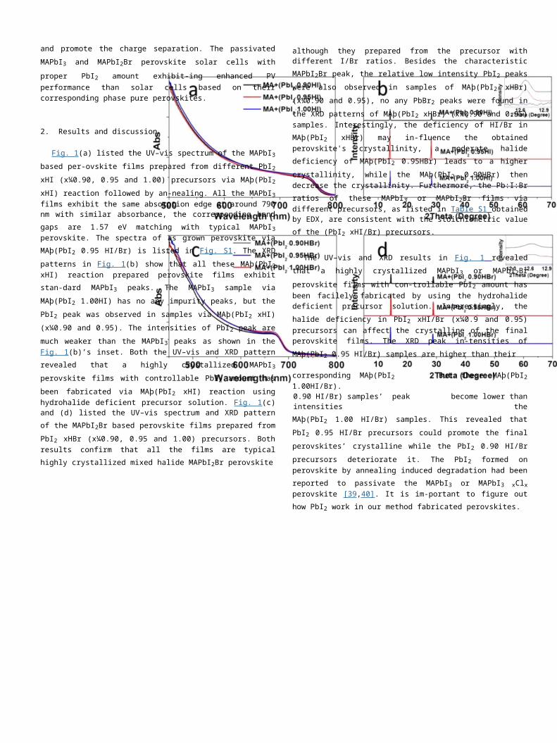
Fig. 1(a) listed the UV–vis spectrum of the MAPbI3 based per-ovskite films prepared from different PbI2 xHI (x¼0.90, 0.95 and 1.00) precursors via MAþ(PbI2 xHI) reaction followed by an-nealing. All the MAPbI3 films exhibit the same absorption edge at around 790 nm with similar absorbance, the corresponding band gaps are 1.57 eV matching with typical MAPbI3
perovskite. The spectra of as grown perovskite via MAþ(PbI2 0.95 HI/Br) is listed in Fig. S1. The XRD patterns in Fig. 1(b) show that all these MAþ(PbI2
xHI) reaction prepared perovskite films exhibit stan-dard MAPbI3 peaks. The MAPbI3 sample via MAþ(PbI2 1.00HI) has no any impurity peaks, but the PbI2 peak was observed in samples via MAþ(PbI2 xHI) (x¼0.90 and 0.95). The intensities of PbI2 peak are much weaker than the MAPbI3 peaks as shown in the Fig. 1(b)’s inset. Both the UV–vis and XRD pattern revealed that a highly crystallized MAPbI3 perovskite films with controllable PbI2
amount has been fabricated via MAþ(PbI2 xHI) reaction using hydrohalide deficient precursor solution. Fig. 1(c) and (d) listed the UV–vis spectrum and XRD pattern of the MAPbI2Br based perovskite films prepared from PbI2 xHBr (x¼0.90, 0.95 and 1.00) precursors. Both results confirm that all the films are typical highly crystallized mixed halide MAPbI2Br perovskite
although they prepared from the precursor with different I/Br ratios. Besides the characteristic MAPbI2Br peak, the relative low intensity PbI2 peaks were also observed in samples of MAþ(PbI2 xHBr) (x¼0.90 and 0.95), no any PbBr2 peaks were found in the XRD patterns of MAþ(PbI2 xHBr) (x¼0.90 and 0.95) samples. Interestingly, the deficiency of HI/Br in MAþ(PbI2 xHBr) may in-fluence the obtained perovskite's crystallinity, a moderate halide deficiency of MAþ(PbI2 0.95HBr) leads to a higher crystallinity, while the MAþ(PbI2 0.90HBr) then decrease the crystallinity. Furthermore, the Pb:I:Br ratios of these MAPbI3 or MAPbI2Br films via different precursors, as listed in Table S1 obtained by EDX, are consistent with the stoichiometric value of the (PbI2 xHI/Br) precursors.
The UV–vis and XRD results in Fig. 1 revealed that a highly crystallized MAPbI3 or MAPbI2Br perovskite films with con-trollable PbI2 amount has been facilely fabricated by using the hydrohalide deficient precursor solution. Interestingly, the halide deficiency in PbI2 xHI/Br (x¼0.9 and 0.95) precursors can affect the crystalline of the final perovskite films. The XRD peak in-tensities of MAþ(PbI2 0.95 HI/Br) samples are higher than their
corresponding MAþ(PbI2 1.00HI/Br). But these MAþ(PbI20.90 HI/Br) samples’ peak intensities become lower than the
MAþ(PbI2 1.00 HI/Br) samples. This revealed that PbI2 0.95 HI/Br precursors could promote the final perovskites’ crystalline while the PbI2 0.90 HI/Br precursors deteriorate it. The PbI2 formed on perovskite by annealing induced degradation had been reported to passivate the MAPbI3 or MAPbI3 xClx
perovskite [39,40]. It is im-portant to figure out how PbI2 work in our method fabricated perovskites.
Fig. 1. (A) UV–vis absorption spectra and (B) XRD patterns of MAPbI3 based perovskite films prepared from MAþ(PbI2 xHI) reaction, inset is the detailed PbI2 peaks; (C) UV– vis absorption
spectra and (D) XRD patterns of MAPbI2Br based perovskite films prepared from MAþ(PbI2 xHBr) reaction, inset is the detailed PbI2 peaks.
52 T. Zhang et al. / Nano Energy 26 (2016) 50–56
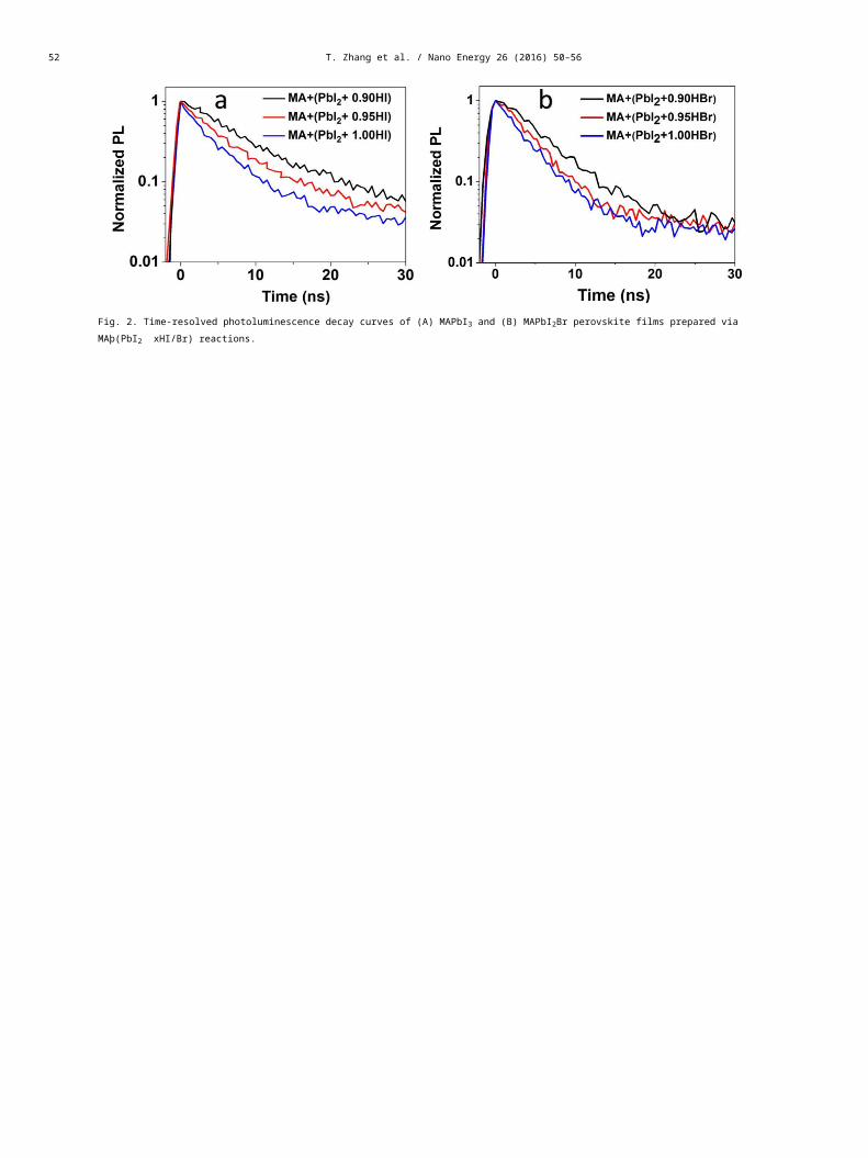
Fig. 2. Time-resolved photoluminescence decay curves of (A) MAPbI3 and (B) MAPbI2Br perovskite films prepared via MAþ(PbI2 xHI/Br) reactions.

Fig. 2 list the time-resolved photoluminescence decay curves of the MAPbI3 and MAPbI2Br perovskite films via three typical PbI2 xHI/Br precursors (x¼0.90, 0.95 and 1.00). The MAPbI3 or MAPbI2Br perovskite films with PbI2 composition prepared from both PbI2 0.95 HI/Br and PbI2 0.90 HI/Br precursors show the longer PL lifetime than their corresponding pure perovskite films prepared by PbI2 1.00 HI/Br precursors. The observed longer PL lifetimes suggested that the MAPbI3 or MAPbI2Br perovskites has been effectively passivate by the PbI2, which is similar to previous reports [39,40]. In the previous reports, the PbI2 crystals locate between the grain boundary of MAPbI3 or MAPbI3 xClx crystals [40]. It is necessary to study these different MAPbI3 or MAPbI2Br perovskite films’ morphologies because perovskite films’ crystal size and morphology can affect their PL lifetimes same as the lo-cation of PbI2 crystals.
The SEM images reveal that MAPbI3 perovskite films prepared from different PbI2 xHI precursors are compact and uniform; the perovskite crystals’ grain sizes are about several hundred nm as shown in Fig. 3. All these perovskite films are about 350 nm thick as illustrated in the cross-section SEM images. No obvious grain size difference is observed in these MAPbI3 perovskite planar films prepared from different PbI2 xHI precursors. However, the MAþ(PbI2 0.90HI) and MAþ(PbI2 0.95HI) prepared MAPbI3 perovskite films are full of small unknown bright nanoplate pieces between perovskite crystals’ grain boundary as illustrated in Fig. S2. The morphology and location of these bright nanoplate pieces are similar to previously reported PbI2 crystals in the annealing or solvent engineering prepared PbI2 passivated perovskite films [35,40]. Furthermore, these characteristic bright pieces disappear in the PbI2 1.00HI precursor fabricated phase pure MAPbI3 per-ovskite film. It seems that these bright nanoplate pieces are highly like to be PbI2 crystals. The EDS analysis on these bright nano-plates label by red circles has revealed a ∼2:1 M ratio of Pb/I in both the PbI2 xHI/Br (x¼0.95) samples as illustrated in Fig. S3, which confirm that these bright nanoplates should be PbI2. The grain size and morphology of the MAPbI2Br perovskite films via different PbI2 xHI/Br precursors (x¼0.90, 0.95 and 1.00) are also compact and uniformed. Similar to PbI2 in MAPbI3 sample, the bright PbI2
nanocrystals also located in the grain boundary. The SEM images have revealed that the PbI2 crystals all locate at the grain boundary between perovskite crystals in our hydrohalide deficient PbI2 xHI/Br (x¼0.90, 0.95) precursor prepared per-ovskite films, which is consistent with their longer PL lifetime due to the PbI2 passivation. The pinholes formed in the PbI2 0.90 HI/Br perovskite samples is more than the PbI2 0.95 HI/Br samples, as shown in Fig. S4, which is consistent with their different re-producibility in the PV performance including Voc as discussed
later. In previous report, the PbI2 locate at the grain boundary of annealed MAPbI3 or MAPbI3 xClx perovskites because the thermal degradation of MAPbI3 or MAPbI3 xClx perovskite usually taken place at surface due to surface energy. Here, our perovskite films are formed by reacting MA gas with PbI2 xHI/Br precursors fol-lowed by annealing, this reaction should be initiated from surface. It is necessary to figure out the formation mechanism of PbI2 in our methods.
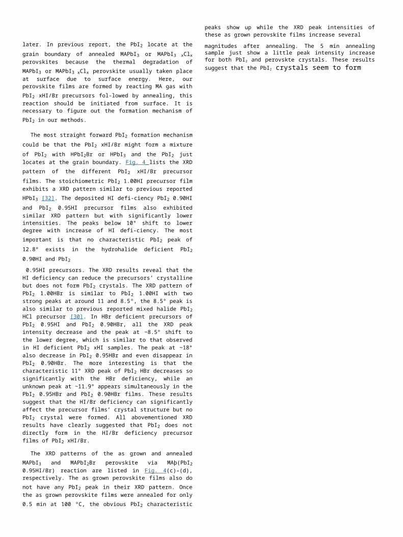
The most straight forward PbI2 formation mechanism could be that the PbI2 xHI/Br might form a mixture of PbI2 with HPbI2Br or HPbI3 and the PbI2 just locates at the grain boundary. Fig. 4 lists the XRD pattern of the different PbI2 xHI/Br precursor films. The stoichiometric PbI2 1.00HI precursor film exhibits a XRD pattern similar to previous reported HPbI3 [32]. The deposited HI defi-ciency PbI2 0.90HI and PbI2 0.95HI precursor films also exhibited similar XRD pattern but with significantly lower intensities. The peaks below 10° shift to lower degree with increase of HI defi-ciency. The most important is that no characteristic PbI2 peak of 12.8° exists in the hydrohalide deficient PbI2 0.90HI and PbI2
0.95HI precursors. The XRD results reveal that the HI deficiency can reduce the precursors’ crystalline but does not form PbI2 crystals. The XRD pattern of PbI2 1.00HBr is similar to PbI2 1.00HI with two strong peaks at around 11 and 8.5°, the 8.5° peak is also similar to previous reported mixed halide PbI2
HCl precursor [30]. In HBr deficient precursors of PbI2 0.95HI and PbI2
0.90HBr, all the XRD peak intensity decrease and the peak at ∼8.5° shift to the lower degree, which is similar to that observed in HI deficient PbI2 xHI samples. The peak at ∼18° also decrease in PbI2 0.95HBr and even disappear in PbI2 0.90HBr. The more interesting is that the characteristic 11° XRD peak of PbI2 HBr decreases so significantly with the HBr deficiency, while an unknown peak at ∼11.9° appears simultaneously in the PbI2 0.95HBr and PbI2 0.90HBr films. These results suggest that the HI/Br deficiency can significantly affect the precursor films’ crystal structure but no PbI2 crystal were formed. All abovementioned XRD results have clearly suggested that PbI2 does not directly form in the HI/Br deficiency precursor films of PbI2
xHI/Br.
The XRD patterns of the as grown and annealed MAPbI3 and MAPbI2Br perovskite via MAþ(PbI2 0.95HI/Br) reaction are listed in Fig. 4(c)–(d), respectively. The as grown perovskite films also do not have any PbI2 peak in their XRD pattern. Once the as grown perovskite films were annealed for only 0.5 min at 100 °C, the obvious PbI2 characteristic peaks show up while the XRD peak intensities of these as grown perovskite films increase several
magnitudes after annealing. The 5 min annealing sample just show a little peak intensity increase for both PbI2 and perovskte crystals. These results suggest that the PbI2 crystals seem to form
T. Zhang et al. / Nano Energy 26 (2016) 50–56 53
Fig. 3. Top view and cross section (insert) SEM images of MAPbI3 prepared from MAþ(PbI2 xHI) (x¼0.90 (a), 0.95 (b) and 1.00 (c) and MAPbI2Br prepared from MAþ(PbI2 xHBr) (x¼0.90 (d),
0.95 (e) and 1.00 (f). scale bar: 1 mm. Typical bright PbI2nanoplates are labeled with red circles.
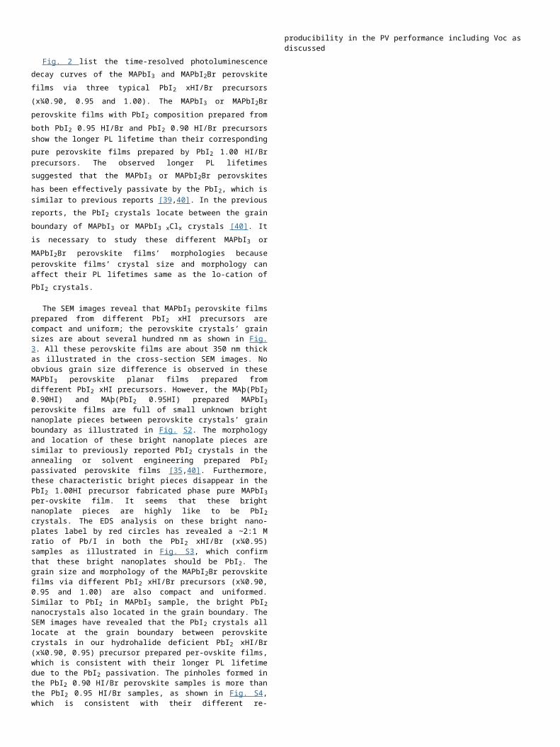
Fig. 4. XRD patterns of(A) PbI2 xHI and (B) PbI2 xHBr precursor films; XRD evolution of (C) MAPbI3 and (D) MAPbI2Br prepared from MAþ(PbI2 0.95HI/Br) reaction by annealing at 100 °C for different time, inset is the detailed PbI2 peaks.
54 T. Zhang et al. / Nano Energy 26 (2016) 50–56
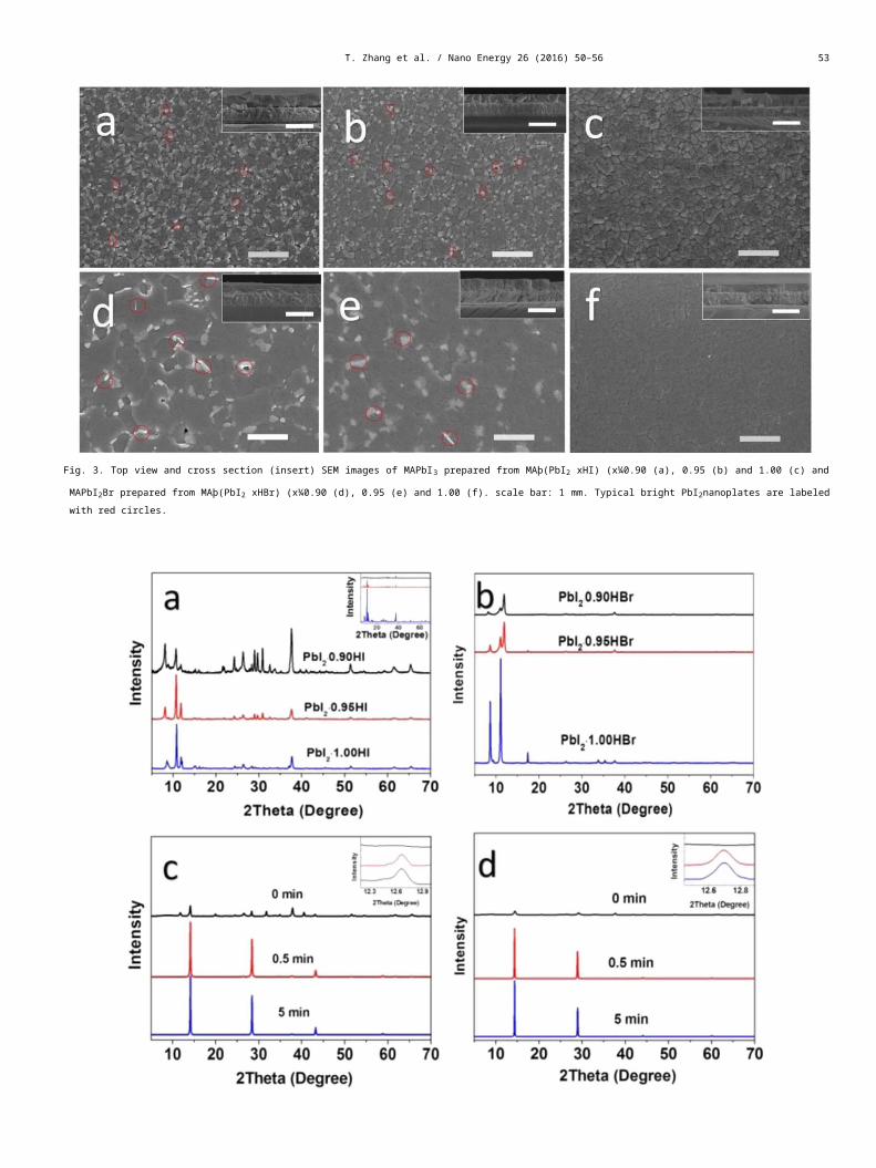
Fig. 5. Typical J-V curves of (a) MAPbI3 and (b) MAPbI2Br based on perovskite films prepared from MAþ(PbI2 xHI) reaction; (c) The incident photon-to-current ef ficiency (IPCE) and stable output at maximum point (d) of MAPbI3 and MAPbI2Br perovskite solar cells via [MA(g) þPbI2 þ0.95 HI/Br] (Integrated Jsc from (c) are 20.42 mA/cm 2 and 16.97 mA/cm 2 for PbI2 passivated MAPbI3
and MAPbI2Br solar cells, respectively ).
during the annealing crystallization process. We hypothesis that the PbI2 crystals are highly like to form between perovskite crys-tal’s grain boundary during the annealing crystallization. Although we could not completely exclude the possibility of forming PbI2 via thermal degradation, we prefer to that the formation of PbI2 is mainly not from thermal degradation of perovskite because the 5 min annealing is widely adopted to prepared phase pure per-ovskite and the 5 min annealled MAþ(PbI2 1.00HI/Br) samples do not show any PbI2 peaks.
Abovementioned material characterizations have confirmed that we could use the hydrohalide deficient PbI2 xHI/Br precursors to fabricate PbI2
passivated MAPbI2X (X¼I/Br) perovskite with con-trollable amount of PbI2 locating at grain boundary. Here we adopted a planar configuration to fabricate solar cells based these perovskite planar films. Fig. 5(a) and (b) lists the typical JV curves of the MAPbI2X (X¼I/Br)solar cells, which are highly dependent on the PbI2amounts. Solar cells based on PbI2 passivated MAPbI3
and MAPbI2Br perovskites using PbI2 0.95HI/Br precursors exhibited better performances than their corresponding phase pure perovskite solar cells especially the enhanced Voc. The improved Voc could be attributed to suppressed charge recombination due to the PbI2 passivation. However, too much PbI2 could show the negative effect. The solar cells based on MAþPbI2
0.90HI/Br prepared perovskites films with more PbI2 exhibit dete-riorated performances in Jsc or FF. The deterioration of photovoltaic performances could be ascribed to the reduced crystalline in per-ovskite films, more pinholes or the hindered electron transport by PbI2. The champion PbI2
passivated MAPbI3 based devices prepared via MAþPbI2 0.95HI exhibited an efficiency of 17.74% with Voc ¼ 1.10 V, Jsc ¼20.94 mA cm 2 and FF¼0.77 as shown in Table S2. Inter-estingly, the champion PbI2 passivated mixed halide MAPbI2Br solar
cells are also based on the MAþPbI2 0.95HBr fabricated perovskites, which exhibit the highest efficiency of 14.45% with Voc ¼ 1.16 V, Jsc ¼ 17.07 mA cm 2, and FF ¼ 0.73. The Jsc of both champion cells are well consistent with their IPCE as shown in Fig. 5(c). It is worth mentioning that the IPCE value of PbI2 passivated MAPbI2Br solar cell via MAþPbI2
0.95HBr has reached up to 86% at a wide spectral range, while the MAþPbI2 0.90HBr fabricated MAPbI2Br solar cell’s IPCE is less than 80% as shown in Fig. S5, although the two perovskite films with dif-ferent PbI2
amount has almost the same absorbance. All these suggest that too much PbI2
could deteriorate the charge separation or electron transfer due to PbI2’s one magnitude lower electron transfer proper-ties. The stable outputs of both champion cells as shown in Fig. 5(d) are closed to their corresponding maximum efficiency value, whichis consistent with previous report and hysteresis shown in Fig. S6 [29,44–46]. These champion cells based on MAþPbI2 0.95HBr/I per-ovskites are relatively stable when stored in dry air up to two weeks as shown in Fig. S7, the PbI2 passivated MAPbI3 perovskite via MAþPbI2 0.95HI also stable in term of XRD and UV–vis spectrum upon 6 h 1.5 A.M. illumination under ambient condition as shown in Fig. S8.
3. Conclusion
In summary, we demonstrate a novel approach to fabricate MAPbI3 and MAPbI2Br perovskites passivated with controllable PbI2 amount by using hydrohalide deficient PbI2 xHI/Br (xo1) precursors via reaction them with CH3NH2. The amount of PbI2 can be controlled by adjusting the halide deficiency in the PbI2 xHI/Br (xo1) precursors. The PbI2 crystals are highly like to form in the annealing crystallization process rather than exist in the PbI2 xHI/
T. Zhang et al. / Nano Energy 26 (2016) 50–56 55

Br precursor film or as grown perovskite films based on the XRD investigation. The PbI2 crystals locate at the perovskite crystals’ grain boundary to effectively passivate the perovskite, which re-sult in a longer PL lifetime. Both MAPbI3 and MAPbI2Br perovskite solar cells via MAþ(PbI2 0.95HI/Br) exhibit improved PV perfor-mance with the enhanced Voc due to less charge recombination by PbI2 passivation. In contrast, the MAþ(PbI2 0.90HI/Br) samples fabricated solar cells exhibited lower efficiency with worse fill factor or lower Jsc due to the perovskites’ reduced crystalline or the retarded electron transfer by too much PbI2 crystals. In all, we successfully fabricated of controllable PbI2 passivated lead halide perovskites for high performance solar cells especially a 14.4% ef-ficient MAPbI2Br solar cell exhibiting 86% IPCE.
Acknowledgment
YZ acknowledges the support of the NSFC (Grants 51372151 and 21303103) and Houyingdong Fund (151046).
Appendix A. Supplementary material
Supplementary data associated with this article can be found in the online version at http://dx.doi.org/10.1016/j.nanoen.2016.05. 003.
References
[1] A. Kojima, K. Teshima, Y. Shirai, T. Miyasaka, J. Am. Chem. Soc. 131 (2009) 6050 – 6051 .
[2] J.-H. Im, C.-R. Lee, J.-W. Lee, S.-W. Park, N.-G. Park, Nanoscale 3 (2011) 4088 – 4093 .
[3] N.J. Jeon, J.H. Noh, Y.C. Kim, W.S. Yang, S. Ryu, S.I. Seok, Nat. Mater. 13 (2014) 897 – 903 .
[4] J. Burschka, N. Pellet, S.J. Moon, R. Humphry-Baker, P. Gao, M.K. Nazeeruddin, M. Gratzel, Nature 499 (2013) 316 – 319 .
[5] M.M. Lee, J. Teuscher, T. Miyasaka, T.N. Murakami, H.J. Snaith, Science 338 (2012) 643 – 647 .
[6] R.F. Service, Science 344 (2014) 458 . [7] H.-S. Kim, C.-R. Lee, J.-H. Im, K.-B. Lee, T. Moehl, A. Marchioro, S.-J. Moon,
R. Humphry-Baker, J.-H. Yum, J.E. Moser, M. Gratzel, N.-G. Park, Sci. Rep. 2 (2012) 1 – 7 .
[8] T. Zhang, Y. Zhao, Acta Chim. Sinica. 73 (2015) 202 – 210 . [9] W. Chen, Y. Wu, Y. Yue, J. Liu, W. Zhang, X. Yang, H. Chen, E. Bi, I. Ashraful,
M. Grätzel, L. Han, Science 350 (2015) 944 – 948 . [10] J. You, L. Meng, T.-B. Song, T.-F. Guo, Y. Yang, W.-H. Chang, Z. Hong, H. Chen,
H. Zhou, Q. Chen, Y. Liu, N. De Marco, Y. Yang, Nat. Nanotechnol. 11 (2015) 75 – 81 .
[11] A. Mei, X. Li, L. Liu, Z. Ku, T. Liu, Y. Rong, M. Xu, M. Hu, J. Chen, Y. Yang, M. Grätzel, H. Han, Science 345 (2014) 295 – 298 .
[12] X. Li, M. Tschumi, H. Han, S.S. Babkair, R.A. Alzubaydi, A.A. Ansari, S.S. Habib, M.K. Nazeeruddin, S.M. Zakeeruddin, M. Grätzel, Energy Technol. 3 (2015) 551 – 555 .
[13] X. Li, M. Ibrahim Dar, C. Yi, J. Luo, M. Tschumi, S.M. Zakeeruddin, M. K. Nazeeruddin, H. Han, M. Grätzel, Nat. Chem. 7 (2015) 703 – 711 .
[14] Y. Zhao, K. Zhu, J. Phys. Chem. Lett. 5 (2014) 4175 – 4186 . [15] B.-J. Kim, dH. Kim, Y.-Y. Lee, H.-W. Shin, G.S. Han, J.S. Hong, K. Mahmood,
T. Ahn, Y.-C. Joo, K.S. Hong, N.-G. Park, S. Lee, H.S. Jung, Energy Environ. Sci. 8 (2014) 916 – 921 .
[16] W.-J. Yin, T. Shi, Y. Yan, Adv. Mater. 26 (2014) 4653 – 4658 . [17] W. Ke, G. Fang, J. Wan, H. Tao, Q. Liu, L. Xiong, P. Qin, J. Wang, H. Lei, G. Yang,
M. Qin, X. Zhao, Y. Yan, Nat. Commun. 6 (2015) 6700 . [18] L.K. Ono, S. Wang, Y. Kato, S.R. Raga, Y. Qi, Energy Environ. Sci. 7 (2014)
3989 – 3993 . [19] M. Liu, M.B. Johnston, H.J. Snaith, Nature 501 (2013) 395 – 398 . [20] B. Conings, L. Baeten, C. De Dobbelaere, J. D ’ Haen, J. Manca, H.-G. Boyen, Adv. Mater.
26 (2014) 2041 – 2046 . [21] P.-W. Liang, C.-Y. Liao, C.-C. Chueh, F. Zuo, S.T. Williams, X.-K. Xin, J. Lin, A.K.
Y. Jen, Adv. Mater. 26 (2014) 3748 – 3754 . [22] Y. Zhao, K. Zhu, J. Phys. Chem. Lett. 4 (2013) 2880 – 2884 . [23] J.T. Wang, J.M. Ball, E.M. Barea, A. Abate, J.A. Alexander-Webber, J. Huang,
M. Saliba, I. Mora-Sero, J. Bisquert, H.J. Snaith, R.J. Nicolas, Nano Lett. 14 (2013) 724 – 730 .
[24] H.-S. Kim, J.-W. Lee, N. Yantara, P.P. Boix, S.A. Kulkarni, S. Mhaisalkar,
M. Grätzel, N.-G. Park, Nano Lett. 13 (2013) 2412 – 2417 . [25] J.H. Noh, S.H. Im, J.H. Heo, T.N. Mandal, S.I. Seok, Nano Lett. 13 (2013) 1764 –
1769 . [26] Y. Zhao, K. Zhu, J. Phys. Chem. C 118 (2014) 9412 – 9418 . [27] M. Xiao, F. Huang, W. Huang, Y. Dkhissi, Y. Zhu, J. Etheridge, A. Gray-Weale,
U. Bach, Y.-B. Cheng, L. Spiccia, Angew. Chem. Int. Ed. 53 (2014) 9898 – 9903 . [28] E. Della Gaspera, Y. Peng, Q. Hou, L. Spiccia, U. Bach, J.J. Jasieniak, Y.-B. Cheng, Nano
Energy 13 (2015) 249 – 257 . [29] Q. Xue, G. Chen, M. Liu, J. Xiao, Z. Chen, Z. Hu, X.-F. Jiang, B. Zhang, F. Huang,
W. Yang, H.-L. Yip, Y. Cao, Adv. Energy Mater. 6 (2016) 10.1002/ aenm.201502021 .
[30] G. Li, T. Zhang, Y. Zhao, J. Mater. Chem. A 3 (2015) 19674 – 19678 . [31] K. Liang, D.B. Mitzi, M.T. Prikas, Chem. Mater. 10 (1998) 403 – 411 . [32] F. Wang, H. Yu, H.H. Xu, N. Zhao, Adv. Funct. Mater. 25 (2015) 1120 – 1126 . [33] W.S. Yang, J.H. Noh, N.J. Jeon, Y.C. Kim, S. Ryu, J. Seo, S.I. Seok, Science 348
(2015) 1234 – 1237 . [34] J.-H. Heo, H.J. Han, D. Kim, T. Ahn, S.H. Im, Energy Environ. Sci. 8 (2015) 1602 –
1608 . [35] F. Liu, Q. Dong, M.K. Wong, A.B. Djuri š i ć , A. Ng, Z. Ren, Q. Shen, C. Surya, W.
K. Chan, J. Wang, A.M.C. Ng, C. Liao, H. Li, K. Shih, C. Wei, H. Su, J. Dai, Adv. Energy Mater. 6 (2016) 10.1002/aenm.201502206 .
[36] Y.C. Kim, N.J. Jeon, J.H. Noh, W.S. Yang, J. Seo, J.S. Yun, A. Ho-Baillie, S. Huang, M.A. Green, J. Seidel, T.K. Ahn, S.I. Seok, Adv. Energy Mater. 6 (2016) 10.1002/ aenm.201502104 .
[37] D. Bi, A.M. El-Zohry, A. Hagfeldt, G. Boschloo, ACS Photonics 2 (2015) 589 – 594 . [38] D.H. Cao, C.C. Stoumpos, C.D. Malliakas, M.J. Katz, O.K. Farha, J.T. Hupp, M.
G. Kanatzidis, APL Mater. 2 (2014) 091101 . [39] L. Wang, C. McCleese, A. Kovalsky, Y. Zhao, C. Burda, J. Am. Chem. Soc. 136
(2014) 12205 – 12208 . [40] Q. Chen, H. Zhou, T.-B. Song, S. Luo, Z. Hong, H.-S. Duan, L. Dou, Y. Liu, Y. Yang,
Nano Lett. 14 (2014) 4158 – 4163 . [41] Y. Zhao, A.M. Nardes, K. Zhu, Faraday Discuss. 176 (2014) 301 – 312 . [42] S. Wang, W. Dong, X. Fang, Q. Zhang, S. Zhou, Z. Deng, R. Tao, J. Shao, R. Xia,
C. Song, L. Hu, J. Zhu, Nanoscale 8 (2016) 6600 – 6608 . [43] N. Ahn, D.-Y. Son, I.-H. Jang, S.M. Kang, M. Choi, N.-G. Park, J. Am. Chem. Soc. 137
(2015) 8696 – 8699 . [44] Z. Zhou, Z. Wang, Y. Zhou, S. Pang, D. Wang, H. Xu, Z. Liu, N.P. Padture, G. Cui,
Angew. Chem. Int. Ed. 127 (2015) 9841 – 9845 . [45] S. Gamliel, L. Etgar, RSC Adv. 4 (2014) 29012 – 29021 . [46] G.L. Frey, K.J. Reynolds, R.H. Friend, Adv. Mater. 14 (2002) 265 – 268 .
Taiyang Zhang received his Master degree of Applied chemistry at Shanghai Institute of Technology in 2014. Then he joined Prof. Yixin Zhao's group. He is currently a Ph.D. candidate and his research interests are focused on the synthesis of lead halide perovskite based pho-toelectric materials, solar cell fabrications and the fundamental research of their physical and chemical properties.
Nanjie Guo received his B.S. degree in 2014 in Thermal and Power Engineering from Harbin Institute of Tech-nology. He is currently a master degree Candidate in Environmental Science and Engineering at Shanghai Jiaotong University under the supervision of Prof. Yixin Zhao. His Current Research Interests Are focused on the Screen printable Perovskite Solar Cells.
Ge Li received his B.S. degree in 2015 in Environmental Science and Engineering from Shanghai Jiao Tong Uni-versity. He is currently a master degree candidate in Yixin Zhao's group. His research interests are mainly engaged in the synthesis of perovskite materials.
56 T. Zhang et al. / Nano Energy 26 (2016) 50–56
Prof. Xufang Qian received her Ph.D. Degree under the supervision of Prof. Dongyuan Zhao at Department of Chemistry, Fudan University. She Got the Grant from JSPS and worked as a Research Fellow at the Laboratory of Prof. Hiromi Yamashita, Osaka University. She Is Currently an Associate Professor in the School of En-vironmental Science and Engineering, Shanghai Jiao Tong University Since 2015. Her current research fo-cuses on the development of photocatalytic materials for the study in environment and energy fields.
Professor Yixin Zhao received his BS and MS degree in Chemistry from Shanghai Jiao Tong University at China in 2002 and 2005. He obtained his Ph.D. from Case Western Reserve University in 2010, then he worked as postdoctoral fellow at Pennsylvania State University and National Renewable Energy Laboratory on high efficiency dye sensitized solar cell, organmetal halide perovskite solar cell and photoelectrochemical water splitting cells. Currently, Prof. Zhao focused his research on green energy and environmental chemistry.