1 PC Peripherals for Technicians PC Peripherals for Technicians Chapter 3.1 - Video Subsystem...
42
1 PC Peripherals PC Peripherals for Technicians for Technicians Chapter 3.1 - Chapter 3.1 - Video Video Subsystem Overview Subsystem Overview Systems Manufacturing Systems Manufacturing Training and Employee Training and Employee Development Development Copyright © 1998 Intel Copyright © 1998 Intel Corp. Corp.
-
date post
19-Dec-2015 -
Category
Documents
-
view
237 -
download
5
Transcript of 1 PC Peripherals for Technicians PC Peripherals for Technicians Chapter 3.1 - Video Subsystem...
1
PC PeripheralsPC Peripherals for for TechniciansTechnicians
Chapter 3.1 - Chapter 3.1 - Video Video Subsystem OverviewSubsystem Overview
Systems Manufacturing Training Systems Manufacturing Training and Employee Developmentand Employee Development
Copyright © 1998 Intel Corp.Copyright © 1998 Intel Corp.
2
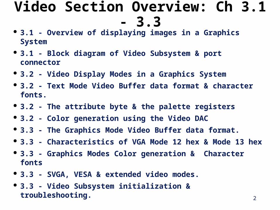
Video Section Overview: Ch 3.1 - 3.3 3.1 - Overview of displaying images in a Graphics System 3.1 - Block diagram of Video Subsystem & port connector 3.2 - Video Display Modes in a Graphics System 3.2 - Text Mode Video Buffer data format & character fonts. 3.2 - The attribute byte & the palette registers 3.2 - Color generation using the Video DAC 3.3 - The Graphics Mode Video Buffer data format. 3.3 - Characteristics of VGA Mode 12 hex & Mode 13 hex 3.3 - Graphics Modes Color generation & Character fonts 3.3 - SVGA, VESA & extended video modes. 3.3 - Video Subsystem initialization & troubleshooting.
3
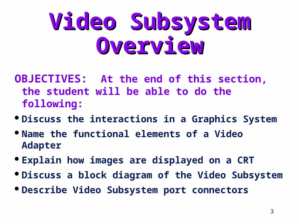
Video SubsystemVideo SubsystemOverviewOverview
OBJECTIVES: At the end of this section, the student will be able to do the following:
Discuss the interactions in a Graphics System Name the functional elements of a Video Adapter Explain how images are displayed on a CRT Discuss a block diagram of the Video Subsystem Describe Video Subsystem port connectors
4
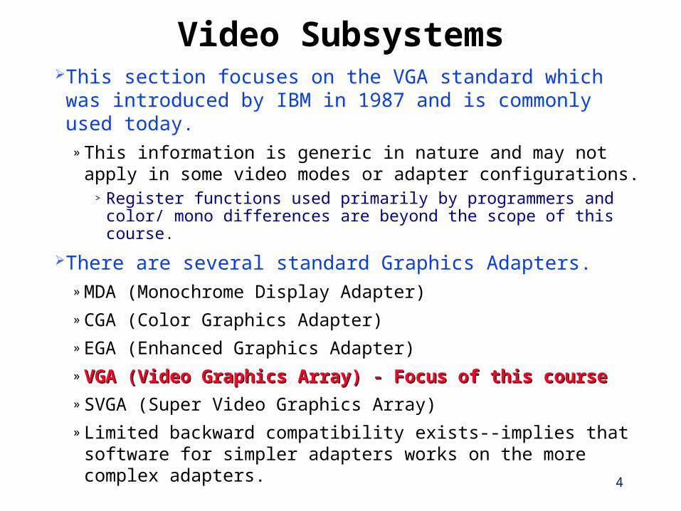
Video SubsystemsThis section focuses on the VGA standard which was
introduced by IBM in 1987 and is commonly used today.» This information is generic in nature and may not apply in
some video modes or adapter configurations.> Register functions used primarily by programmers and color/
mono differences are beyond the scope of this course.
There are several standard Graphics Adapters.» MDA (Monochrome Display Adapter)
» CGA (Color Graphics Adapter)
» EGA (Enhanced Graphics Adapter)
» VGA (Video Graphics Array) - Focus of this courseVGA (Video Graphics Array) - Focus of this course
» SVGA (Super Video Graphics Array)
» Limited backward compatibility exists--implies that software for simpler adapters works on the more complex adapters.
5
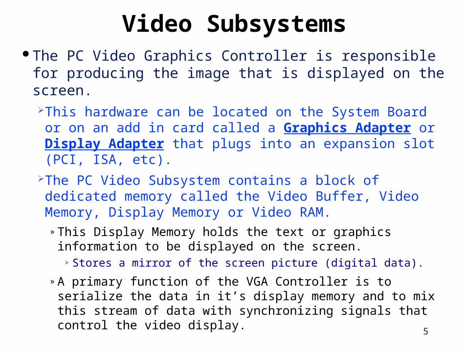
Video Subsystems The PC Video Graphics Controller is responsible for
producing the image that is displayed on the screen.This hardware can be located on the System Board or on
an add in card called a Graphics Adapter or Display Adapter that plugs into an expansion slot (PCI, ISA, etc).
The PC Video Subsystem contains a block of dedicated memory called the Video Buffer, Video Memory, Display Memory or Video RAM.
» This Display Memory holds the text or graphics information to be displayed on the screen.
> Stores a mirror of the screen picture (digital data).
» A primary function of the VGA Controller is to serialize the data in it’s display memory and to mix this stream of data with synchronizing signals that control the video display.
6
Interactions in a Graphics SystemS
OF
TW
AR
E Operating System Applications
BIOS / Graphics Drivers
HA
RD
WA
RE
Microprocessor
PC RAM / ROM
Video Controller
VideoMemory
GraphicsSubsystem
DAC
DISPLAY
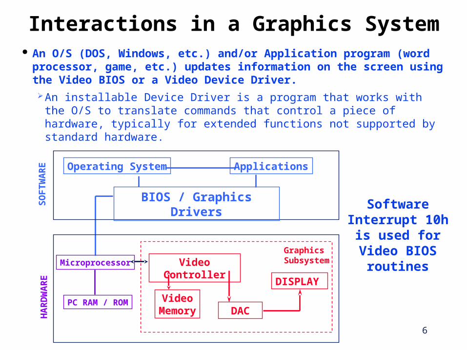
An O/S (DOS, Windows, etc.) and/or Application program (word processor, game, etc.) updates information on the screen using the Video BIOS or a Video Device Driver.An installable Device Driver is a program that works with the O/S to
translate commands that control a piece of hardware, typically for extended functions not supported by standard hardware.
Software Interrupt 10h is used for Video BIOS routines
7
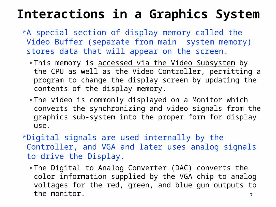
Interactions in a Graphics SystemA special section of display memory called the Video
Buffer (separate from main system memory) stores data that will appear on the screen.
» This memory is accessed via the Video Subsystem by the CPU as well as the Video Controller, permitting a program to change the display screen by updating the contents of the display memory.
» The video is commonly displayed on a Monitor which converts the synchronizing and video signals from the graphics sub-system into the proper form for display use.
Digital signals are used internally by the Controller, and VGA and later uses analog signals to drive the Display.
» The Digital to Analog Converter (DAC) converts the color information supplied by the VGA chip to analog voltages for the red, green, and blue gun outputs to the monitor.
8
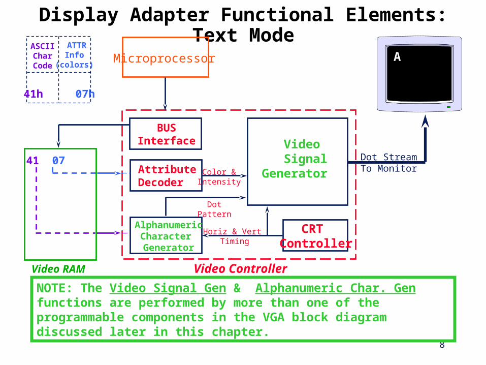
Display Adapter Functional Elements: Text Mode
NOTE: The Video Signal Gen & Alphanumeric Char. Gen functions are performed by more than one of the programmable components in the VGA block diagram discussed later in this chapter.
Dot Stream To Monitor
A
41 07
Video RAM
ASCIICharCode
41h 07h
ATTRInfo
(colors)
Video Controller
Video Signal Generator
CRT Controller
AlphanumericCharacter Generator
AttributeDecoder
Color &Intensity
Dot Pattern
Horiz & Vert Timing
BUSInterface
Microprocessor
9
Display Adapter Functional Elements: Text Mode
The System or Bus Interface :» Decodes memory addresses to Video Memory or I/O
addresses to the VGA registers.
The Cathode Ray Tube Controller (CRTC):» Generates the horizontal and vertical timing signals that
control the path and duration of the electron beam sweeping the inner surface of the CRT.
Display memory» The Video Buffer contains the information to be displayed
on the screen & is effectively a large shift register sending a serial data stream to the monitor.
Alphanumeric Character Generation circuitry:» Translates the ASCII value of a character stored in the
video buffer into a matrix of dots to display on the screen.
10
Display Adapter Functional Elements: Text Mode
The Attribute Decoder:» Controls the color and brightness of the signals sent to the
monitor.
Video Signal Generator:» Outputs the signals that control what appears on the
screen.> Horiz sync (to 90 KHz)> Vert sync (50 - 120Hz)> Three possible kinds of video signals are:
•Digital (CGA, EGA) - Digital RGB monitors accept TTL level signals for red, green, or blue on separate lines.
•Analog (VGA) - Analog RGB monitors accept 0-0.7V analog signals for red, green and blue on separate lines.
•Composite (also used for TV) - The red, green, and blue are combined by the video subsystem and separated by the monitor.
11
Heatingfilament
Horizontaldeflection
coils/plates
Electron beam
PhosphorCoating
Interior metallic coating athigh positive voltage
Vertical deflectioncoils/platesFocusing
system
Controlgrid
(Intensity)
Cathode
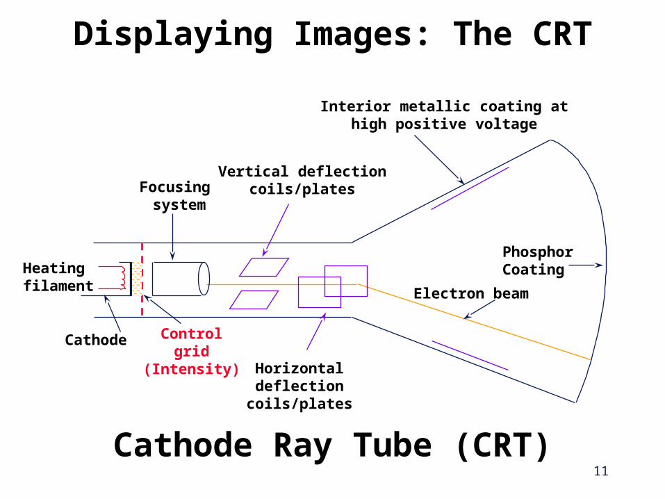
Displaying Images: The CRT
Cathode Ray Tube (CRT)
12
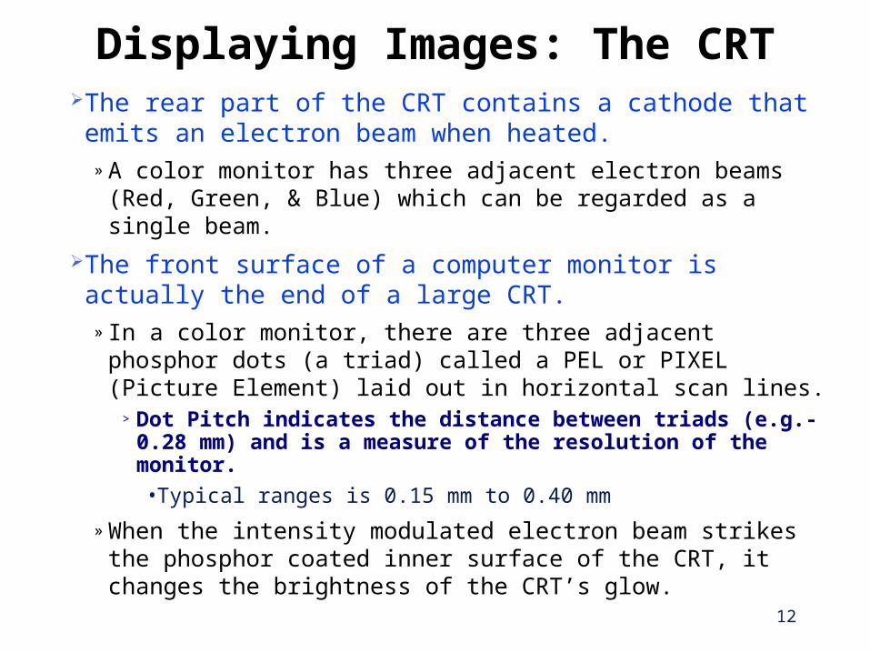
Displaying Images: The CRTThe rear part of the CRT contains a cathode that emits
an electron beam when heated.» A color monitor has three adjacent electron beams (Red,
Green, & Blue) which can be regarded as a single beam.
The front surface of a computer monitor is actually the end of a large CRT.
» In a color monitor, there are three adjacent phosphor dots (a triad) called a PEL or PIXEL (Picture Element) laid out in horizontal scan lines.
> Dot Pitch indicates the distance between triads (e.g.-0.28 mm) and is a measure of the resolution of the monitor.
•Typical ranges is 0.15 mm to 0.40 mm
» When the intensity modulated electron beam strikes the phosphor coated inner surface of the CRT, it changes the brightness of the CRT’s glow.
13
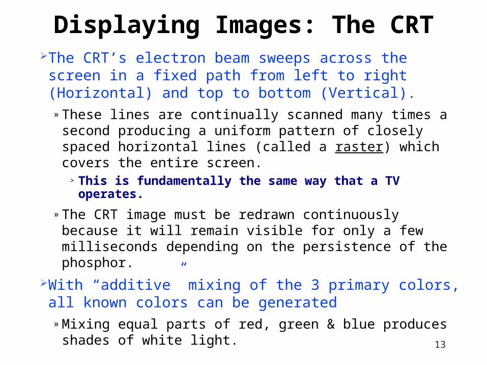
Displaying Images: The CRTThe CRT’s electron beam sweeps across the screen in a
fixed path from left to right (Horizontal) and top to bottom (Vertical).
» These lines are continually scanned many times a second producing a uniform pattern of closely spaced horizontal lines (called a raster) which covers the entire screen.
> This is fundamentally the same way that a TV operates.
» The CRT image must be redrawn continuously because it will remain visible for only a few milliseconds depending on the persistence of the phosphor.
With “additive” mixing of the 3 primary colors, all known colors can be generated
» Mixing equal parts of red, green & blue produces shades of white light.
14
Non-Interlaced and Interlaced Displays Displays are either interlaced or non-interlaced.
In an interlaced graphics system, it takes 2 fields (1 odd, 1 even) to display one complete screen (called a frame)
» Interlaced mode is used when the monitor cannot keep up with the data rates required by the video system--used for the first 1024x768 displays.
A non-interlaced display has an entire frame displayed each screen refresh--every line is updated every frame.
» Non-interlaced displays produce a more pleasing screen image (less flicker) than interlaced displays.
» Quality monitors feature non-interlacing at all resolutions.
» Some monitors can only work in non-interlaced mode up to a maximum pixel addressability (e.g. 800x600) above which they revert to interlaced mode.
15
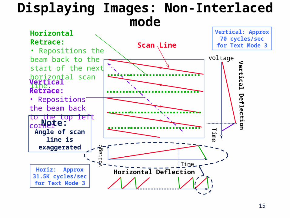
Displaying Images: Non-Interlaced modeHorizontal Retrace:• Repositions the beam back to the start of the next horizontal scan line.
Vertical: Approx70 cycles/sec
for Text Mode 3
Horiz: Approx31.5K cycles/secfor Text Mode 3
Scan Line
Vertical Retrace: • Repositions the beam back to the top left corner
voltage
Ve
rtica
l De
flec
tion
Tim
e
Horizontal DeflectionTimevo
ltage
Note: Angle of scan line
is exaggerated
16
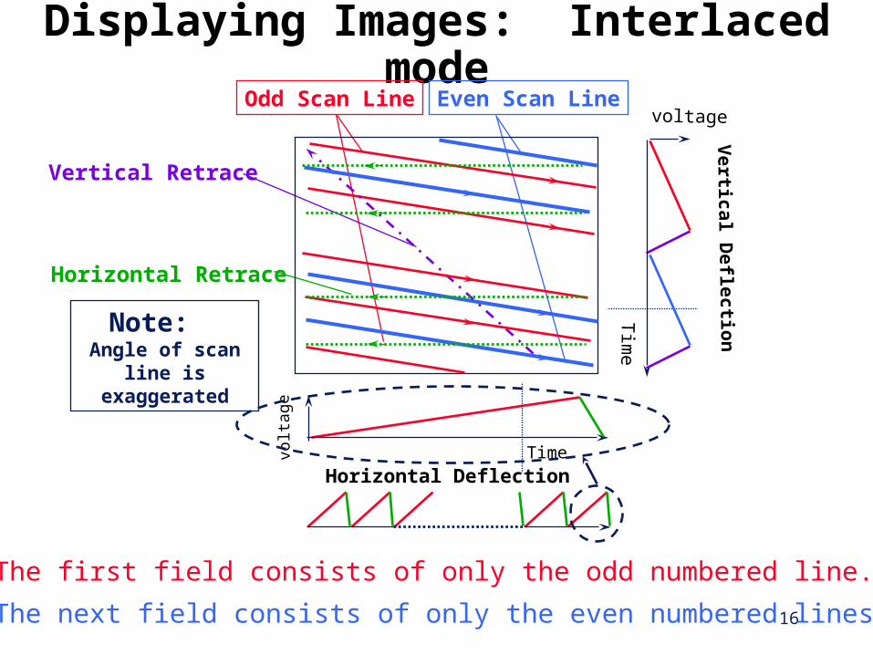
Displaying Images: Interlaced mode
Horizontal Retrace
Note: Angle of scan line
is exaggerated
Vertical Retrace
Odd Scan Line Even Scan Line
Tim
e
voltage
Ve
rtica
l De
flec
tion
Horizontal DeflectionTimevo
ltage
The first field consists of only the odd numbered line.
The next field consists of only the even numbered lines.
17
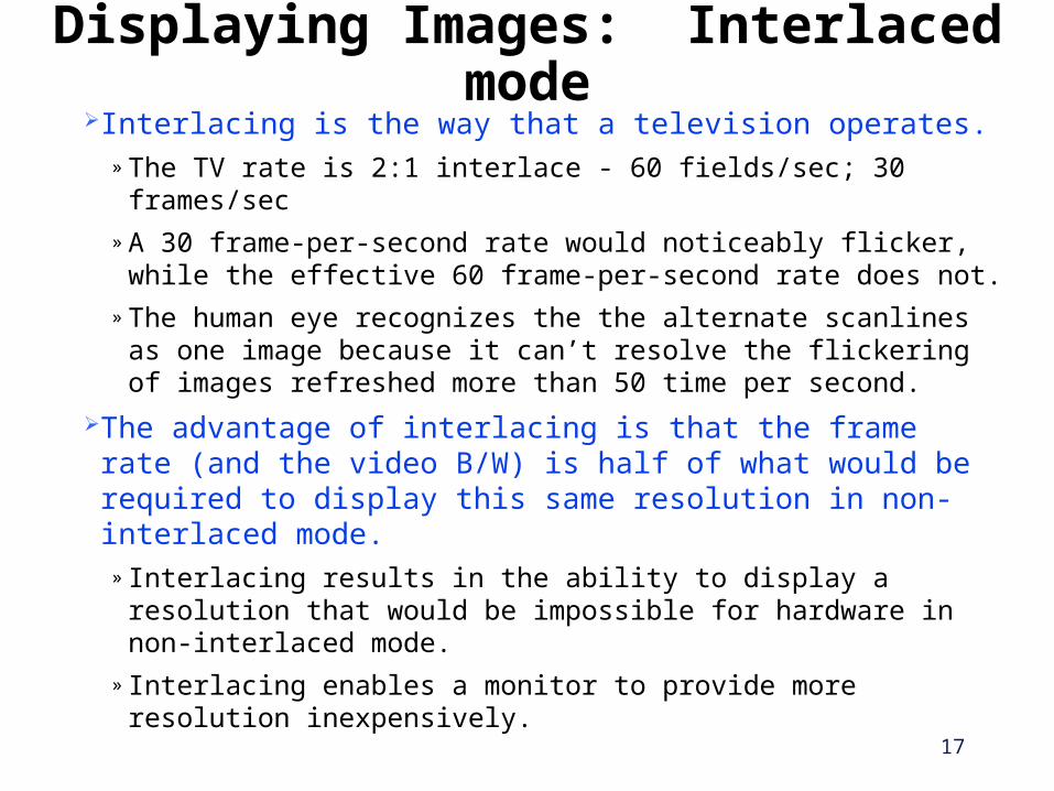
Displaying Images: Interlaced modeInterlacing is the way that a television operates.
» The TV rate is 2:1 interlace - 60 fields/sec; 30 frames/sec
» A 30 frame-per-second rate would noticeably flicker, while the effective 60 frame-per-second rate does not.
» The human eye recognizes the the alternate scanlines as one image because it can’t resolve the flickering of images refreshed more than 50 time per second.
The advantage of interlacing is that the frame rate (and the video B/W) is half of what would be required to display this same resolution in non-interlaced mode.
» Interlacing results in the ability to display a resolution that would be impossible for hardware in non-interlaced mode.
» Interlacing enables a monitor to provide more resolution inexpensively.
18
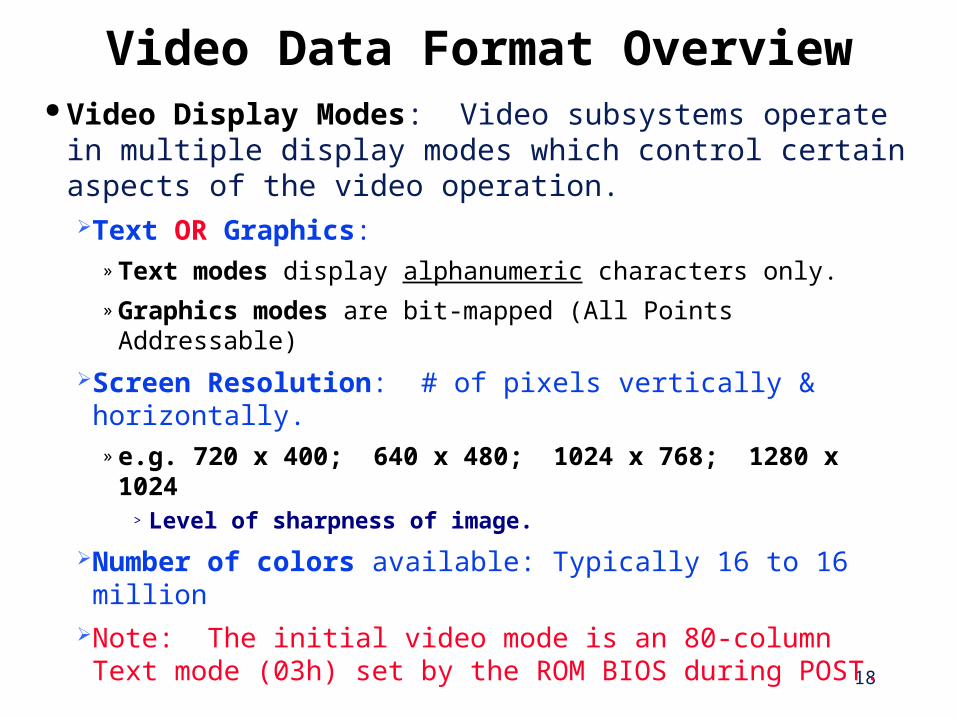
Video Data Format Overview Video Display Modes: Video subsystems operate in
multiple display modes which control certain aspects of the video operation.Text OR Graphics:
» Text modes display alphanumeric characters only.
» Graphics modes are bit-mapped (All Points Addressable)
Screen Resolution: # of pixels vertically & horizontally.» e.g. 720 x 400; 640 x 480; 1024 x 768; 1280 x 1024
> Level of sharpness of image.
Number of colors available: Typically 16 to 16 millionNote: The initial video mode is an 80-column Text mode
(03h) set by the ROM BIOS during POST.
19
Video Data Format Overview The information written to the video buffer by the
microprocessor is represented on the screen as a pattern of illuminated dots called pixels.The microprocessor writes information to the video
hardware’s display buffer in either alphanumeric or graphics format.
Each location on the video screen maps to a location in the display RAM.
> Discussed in more detail in a subsequent chapter.
The first location of the display buffer maps to the top, leftmost point on the screen.
As memory addresses increase, the screen location move from left to right & top to bottom.
20
Video Data Format Overview Alphanumeric format: (Text Mode)
> Discussed in more detail in a subsequent chapter.
The microprocessor writes each symbol (letter, number, etc) as a series of 2 bytes (character & attribute) into the Video Memory.
» The first byte represents the character’s ASCII value
» The second byte represents the character’s attribute (i.e. color, foreground/background, blinking, intensity)
Video hardware translates the character & attribute bytes to the necessary series of dots.
Characters are painted on the screen in a matrix of dots called a character box or character cell.
21
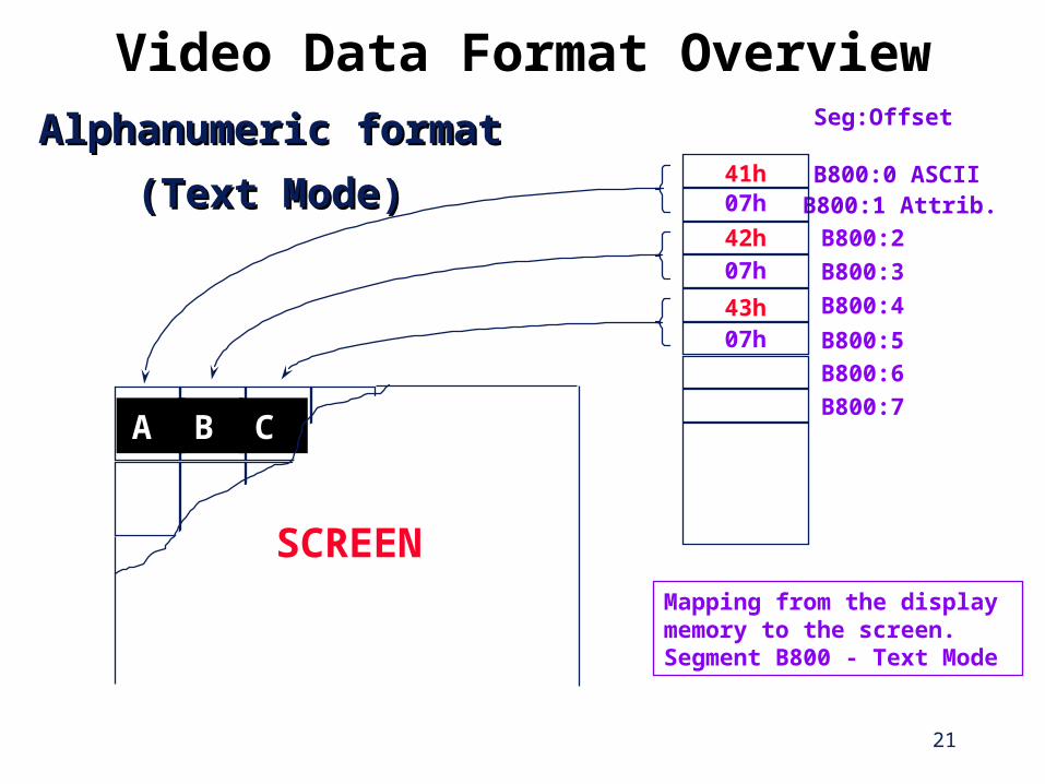
Video Data Format Overview
Mapping from the display memory to the screen. Segment B800 - Text Mode
Seg:Offset
B800:0 ASCII
B800:2
B800:1 Attrib.
B800:3
B800:4
B800:5
B800:6
B800:7
41h
42h
43h
07h
07h
07h
Alphanumeric formatAlphanumeric format
(Text Mode)(Text Mode)
A B C
SCREEN
22
Video Data Format Overview Graphics Mode format:
> Discussed in more detail in a subsequent chapter.
Also known as All Points Addressable (A.P.A.)The microprocessor writes the individual color value of
each pixel to be painted on the screen.» All pixels can be controlled independently to draw
graphics objects (as opposed to Text Mode, in which only a pre-defined set of characters can be displayed.
The microprocessor must address the display buffer as a memory map of a series of bits (bytes for Text mode).
The Video hardware generates the color & control signals necessary to illuminate the dot at the correct location on the screen.
23
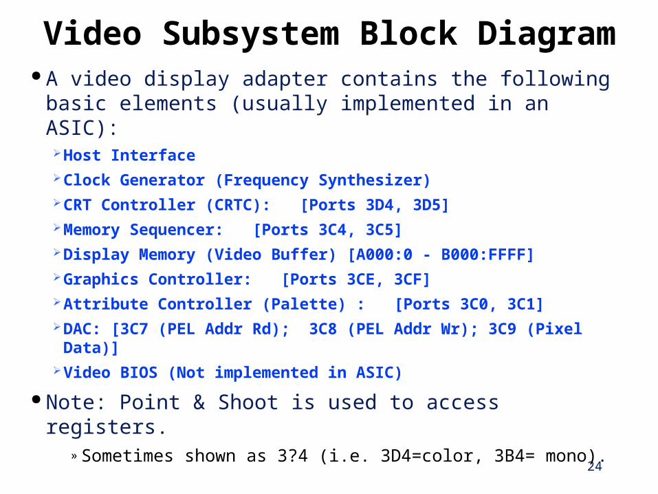
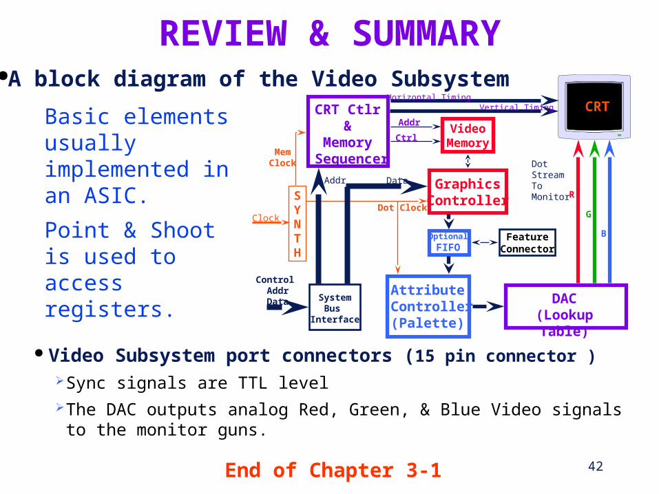
Video Subsystem Block Diagram The following block diagram will introduce the
typical functions of a VGA Video Controller. The following is a generic description to show the
relationship between components of the VGA Video Controller.
Note that many of the components of the video controller interact and this can be represented with different interconnect configurations.You may see the following blocks grouped and/or
connected in different ways, depending on the vendor and the level of detail shown.
24
Video Subsystem Block Diagram A video display adapter contains the following basic
elements (usually implemented in an ASIC):Host InterfaceClock Generator (Frequency Synthesizer)CRT Controller (CRTC): [Ports 3D4, 3D5] Memory Sequencer: [Ports 3C4, 3C5]Display Memory (Video Buffer) [A000:0 - B000:FFFF]Graphics Controller: [Ports 3CE, 3CF]Attribute Controller (Palette) : [Ports 3C0, 3C1]DAC: [3C7 (PEL Addr Rd); 3C8 (PEL Addr Wr); 3C9 (Pixel Data)]Video BIOS (Not implemented in ASIC)
Note: Point & Shoot is used to access registers.» Sometimes shown as 3?4 (i.e. 3D4=color, 3B4= mono).
25
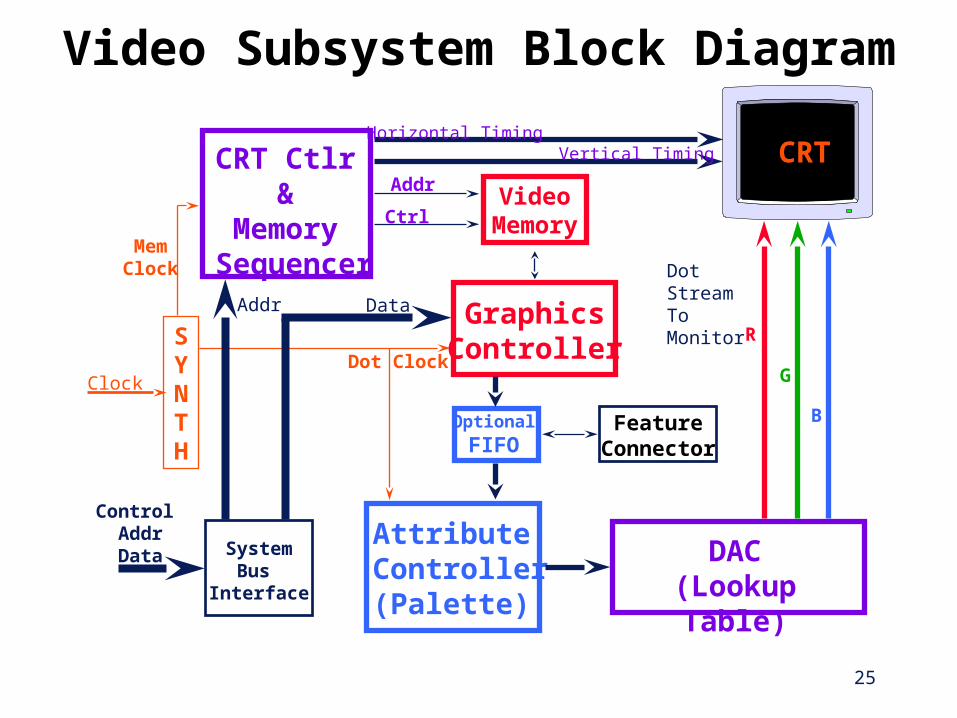
Video Subsystem Block Diagram
Clock
SYNTH
Horizontal TimingVertical Timing
Dot Stream To Monitor
CRTCRT Ctlr&
Memory Sequencer
Optional
FIFO
VideoMemory
GraphicsController
Attribute Controller
(Palette)
SystemBus
Interface
Control AddrData
Addr Data
Addr
Ctrl
FeatureConnector
Dot Clock
MemClock
DAC(Lookup Table)
R
G
B
26
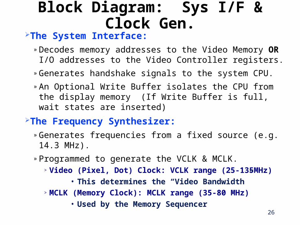
Block Diagram: Sys I/F & Clock Gen.The System Interface:
» Decodes memory addresses to the Video Memory OR I/O addresses to the Video Controller registers.
» Generates handshake signals to the system CPU.
» An Optional Write Buffer isolates the CPU from the display memory (If Write Buffer is full, wait states are inserted)
The Frequency Synthesizer:» Generates frequencies from a fixed source (e.g. 14.3 MHz).
» Programmed to generate the VCLK & MCLK.> Video (Pixel, Dot) Clock: VCLK range (25-135MHz)
• This determines the “Video Bandwidth”> MCLK (Memory Clock): MCLK range (35-80 MHz)
• Used by the Memory Sequencer
27
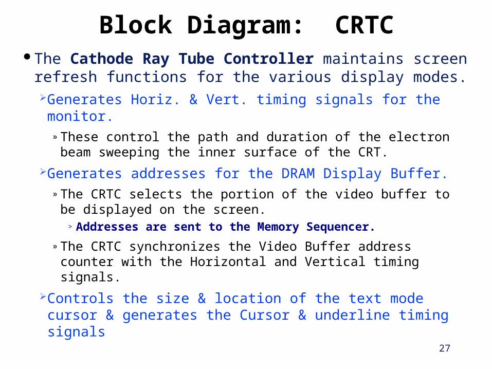
Block Diagram: CRTC The Cathode Ray Tube Controller maintains screen
refresh functions for the various display modes.Generates Horiz. & Vert. timing signals for the monitor.
» These control the path and duration of the electron beam sweeping the inner surface of the CRT.
Generates addresses for the DRAM Display Buffer.» The CRTC selects the portion of the video buffer to be
displayed on the screen.> Addresses are sent to the Memory Sequencer.
» The CRTC synchronizes the Video Buffer address counter with the Horizontal and Vertical timing signals.
Controls the size & location of the text mode cursor & generates the Cursor & underline timing signals
28
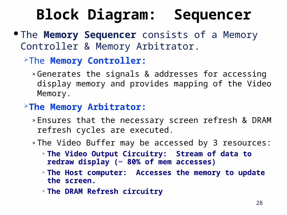
Block Diagram: Sequencer The Memory Sequencer consists of a Memory
Controller & Memory Arbitrator.The Memory Controller:
» Generates the signals & addresses for accessing display memory and provides mapping of the Video Memory.
The Memory Arbitrator:» Ensures that the necessary screen refresh & DRAM refresh
cycles are executed.
» The Video Buffer may be accessed by 3 resources:> The Video Output Circuitry: Stream of data to redraw
display (~ 80% of mem accesses)> The Host computer: Accesses the memory to update the
screen.> The DRAM Refresh circuitry
29
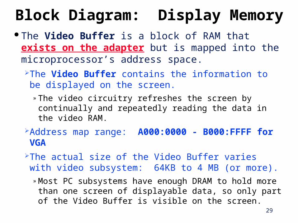
Block Diagram: Display Memory The Video Buffer is a block of RAM that exists on
the adapter but is mapped into the microprocessor’s address space. The Video Buffer contains the information to be
displayed on the screen.» The video circuitry refreshes the screen by continually and
repeatedly reading the data in the video RAM.
Address map range: A000:0000 - B000:FFFF for VGA The actual size of the Video Buffer varies with video
subsystem: 64KB to 4 MB (or more).» Most PC subsystems have enough DRAM to hold more
than one screen of displayable data, so only part of the Video Buffer is visible on the screen.
30
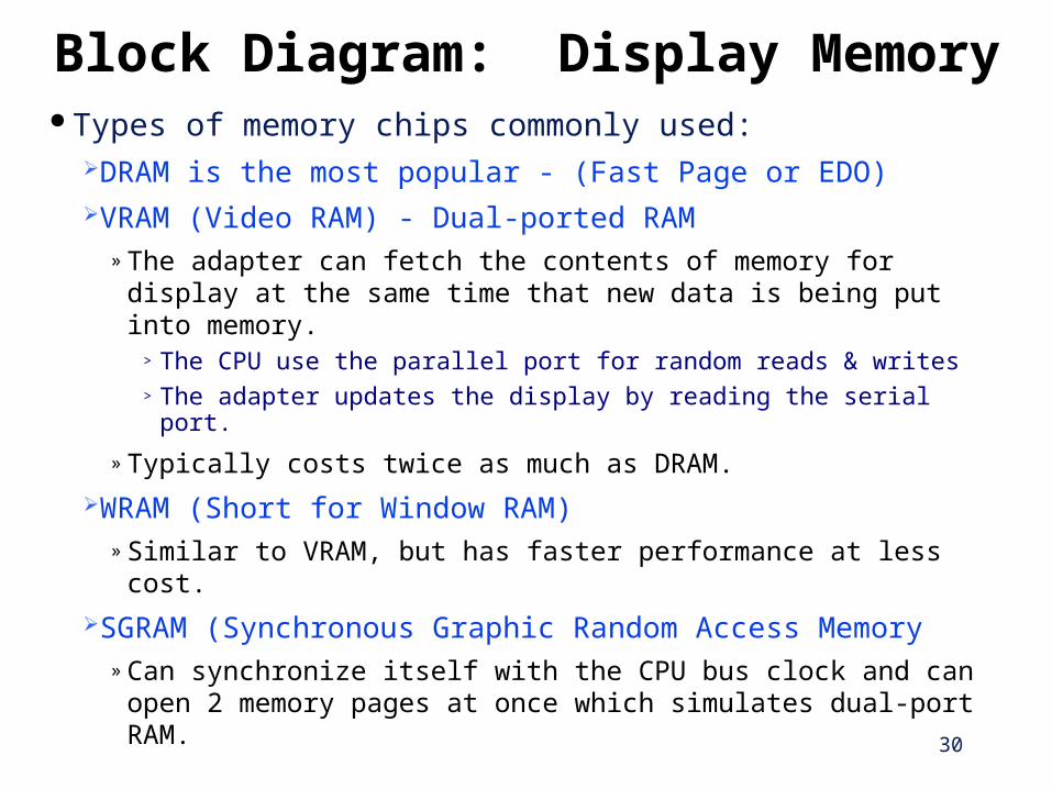
Block Diagram: Display Memory Types of memory chips commonly used:
DRAM is the most popular - (Fast Page or EDO) VRAM (Video RAM) - Dual-ported RAM
» The adapter can fetch the contents of memory for display at the same time that new data is being put into memory.
> The CPU use the parallel port for random reads & writes> The adapter updates the display by reading the serial port.
» Typically costs twice as much as DRAM.
WRAM (Short for Window RAM)» Similar to VRAM, but has faster performance at less cost.
SGRAM (Synchronous Graphic Random Access Memory» Can synchronize itself with the CPU bus clock and can
open 2 memory pages at once which simulates dual-port RAM.
31
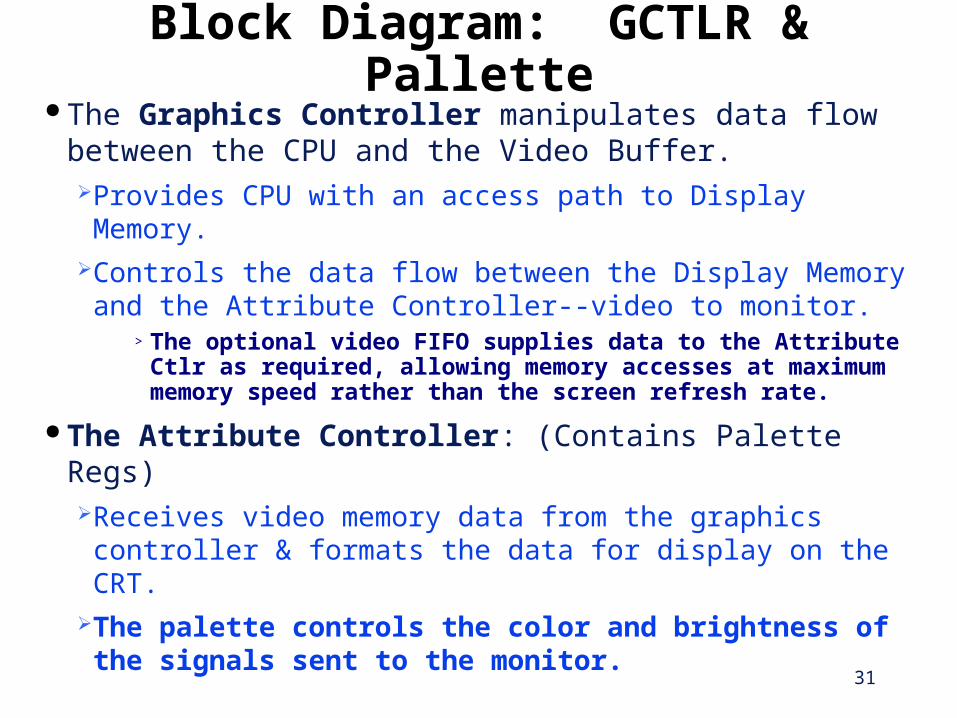
Block Diagram: GCTLR & Pallette The Graphics Controller manipulates data flow
between the CPU and the Video Buffer. Provides CPU with an access path to Display Memory.Controls the data flow between the Display Memory and
the Attribute Controller--video to monitor.> The optional video FIFO supplies data to the Attribute Ctlr
as required, allowing memory accesses at maximum memory speed rather than the screen refresh rate.
The Attribute Controller: (Contains Palette Regs)Receives video memory data from the graphics controller
& formats the data for display on the CRT.The palette controls the color and brightness of the
signals sent to the monitor.
32
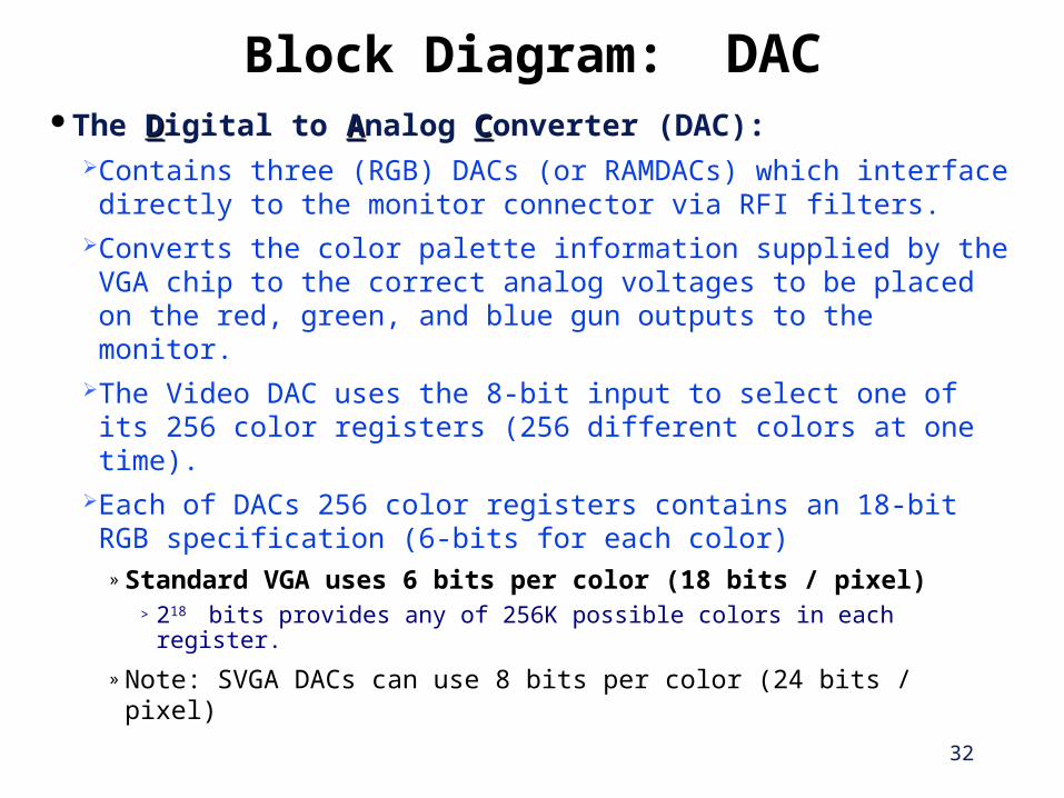
Block Diagram: DAC The DDigital to AAnalog CConverter (DAC):
Contains three (RGB) DACs (or RAMDACs) which interface directly to the monitor connector via RFI filters.
Converts the color palette information supplied by the VGA chip to the correct analog voltages to be placed on the red, green, and blue gun outputs to the monitor.
The Video DAC uses the 8-bit input to select one of its 256 color registers (256 different colors at one time).
Each of DACs 256 color registers contains an 18-bit RGB specification (6-bits for each color)
» Standard VGA uses 6 bits per color (18 bits / pixel)> 218 bits provides any of 256K possible colors in each register.
» Note: SVGA DACs can use 8 bits per color (24 bits / pixel)
33
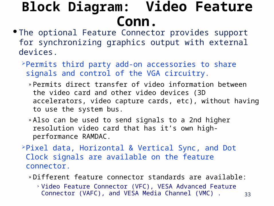
Block Diagram: Video Feature Conn. The optional Feature Connector provides support for
synchronizing graphics output with external devices.Permits third party add-on accessories to share signals
and control of the VGA circuitry.» Permits direct transfer of video information between the
video card and other video devices (3D accelerators, video capture cards, etc), without having to use the system bus.
» Also can be used to send signals to a 2nd higher resolution video card that has it’s own high-performance RAMDAC.
Pixel data, Horizontal & Vertical Sync, and Dot Clock signals are available on the feature connector.
» Different feature connector standards are available: > Video Feature Connector (VFC), VESA Advanced Feature
Connector (VAFC), and VESA Media Channel (VMC) .
34
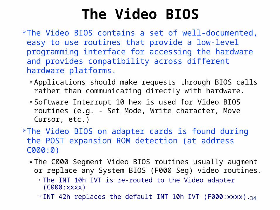
The Video BIOSThe Video BIOS contains a set of well-documented, easy
to use routines that provide a low-level programming interface for accessing the hardware and provides compatibility across different hardware platforms.
» Applications should make requests through BIOS calls rather than communicating directly with hardware.
» Software Interrupt 10 hex is used for Video BIOS routines (e.g. - Set Mode, Write character, Move Cursor, etc.)
The Video BIOS on adapter cards is found during the POST expansion ROM detection (at address C000:0)
» The C000 Segment Video BIOS routines usually augment or replace any System BIOS (F000 Seg) video routines.
> The INT 10h IVT is re-routed to the Video adapter (C000:xxxx)> INT 42h replaces the default INT 10h IVT (F000:xxxx).
35
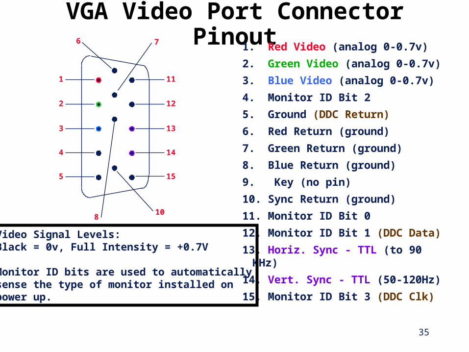
VGA Video Port Connector Pinout1. Red Video (analog 0-0.7v)
2. Green Video (analog 0-0.7v)
3. Blue Video (analog 0-0.7v)
4. Monitor ID Bit 2
5. Ground (DDC Return)
6. Red Return (ground)
7. Green Return (ground)
8. Blue Return (ground)
9. Key (no pin)
10. Sync Return (ground)
11. Monitor ID Bit 0
12. Monitor ID Bit 1 (DDC Data)
13. Horiz. Sync - TTL (to 90 KHz)
14. Vert. Sync - TTL (50-120Hz)
15. Monitor ID Bit 3 (DDC Clk)
1
2
3
4
5 15
14
13
12
11
7
10
6
8
Video Signal Levels: Black = 0v, Full Intensity = +0.7V
Monitor ID bits are used to automaticallysense the type of monitor installed onpower up.
36
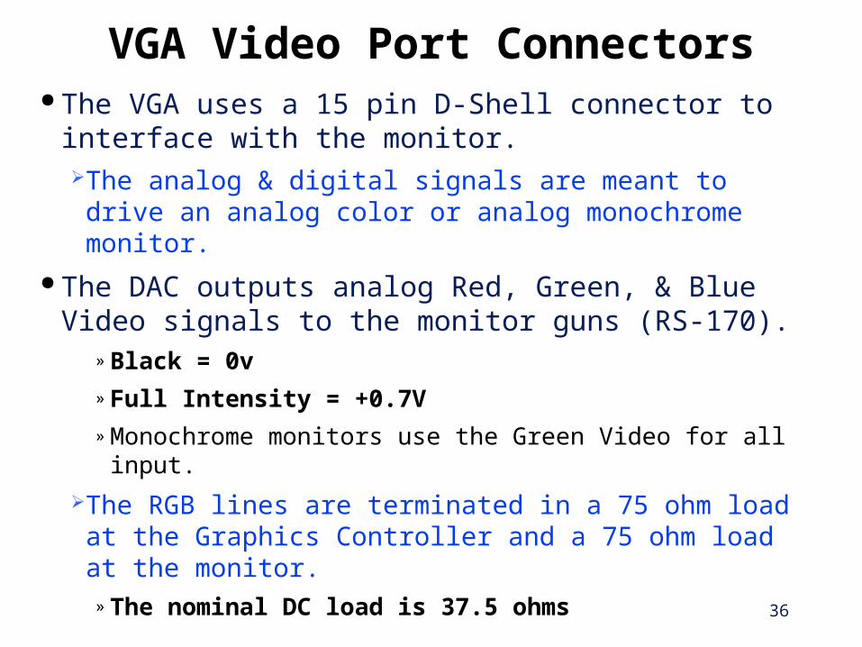
VGA Video Port Connectors The VGA uses a 15 pin D-Shell connector to interface
with the monitor.The analog & digital signals are meant to drive an analog
color or analog monochrome monitor.
The DAC outputs analog Red, Green, & Blue Video signals to the monitor guns (RS-170).
» Black = 0v
» Full Intensity = +0.7V
» Monochrome monitors use the Green Video for all input.
The RGB lines are terminated in a 75 ohm load at the Graphics Controller and a 75 ohm load at the monitor.
» The nominal DC load is 37.5 ohms
37
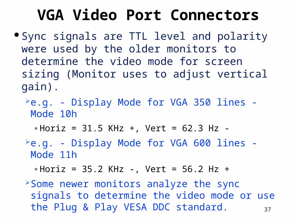
VGA Video Port Connectors Sync signals are TTL level and polarity were used by
the older monitors to determine the video mode for screen sizing (Monitor uses to adjust vertical gain).e.g. - Display Mode for VGA 350 lines - Mode 10h
» Horiz = 31.5 KHz +, Vert = 62.3 Hz -
e.g. - Display Mode for VGA 600 lines - Mode 11h» Horiz = 35.2 KHz -, Vert = 56.2 Hz +
Some newer monitors analyze the sync signals to determine the video mode or use the Plug & Play VESA DDC standard.
38
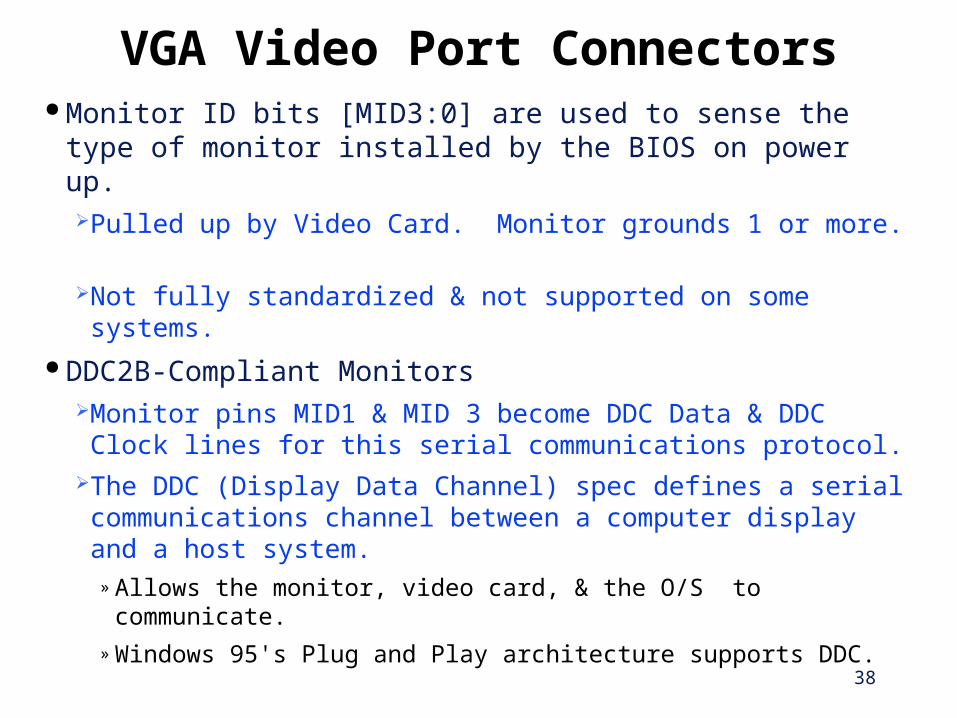
VGA Video Port Connectors Monitor ID bits [MID3:0] are used to sense the type of
monitor installed by the BIOS on power up.Pulled up by Video Card. Monitor grounds 1 or more. Not fully standardized & not supported on some systems.
DDC2B-Compliant Monitors Monitor pins MID1 & MID 3 become DDC Data & DDC
Clock lines for this serial communications protocol.The DDC (Display Data Channel) spec defines a serial
communications channel between a computer display and a host system.
» Allows the monitor, video card, & the O/S to communicate.
» Windows 95's Plug and Play architecture supports DDC.
39
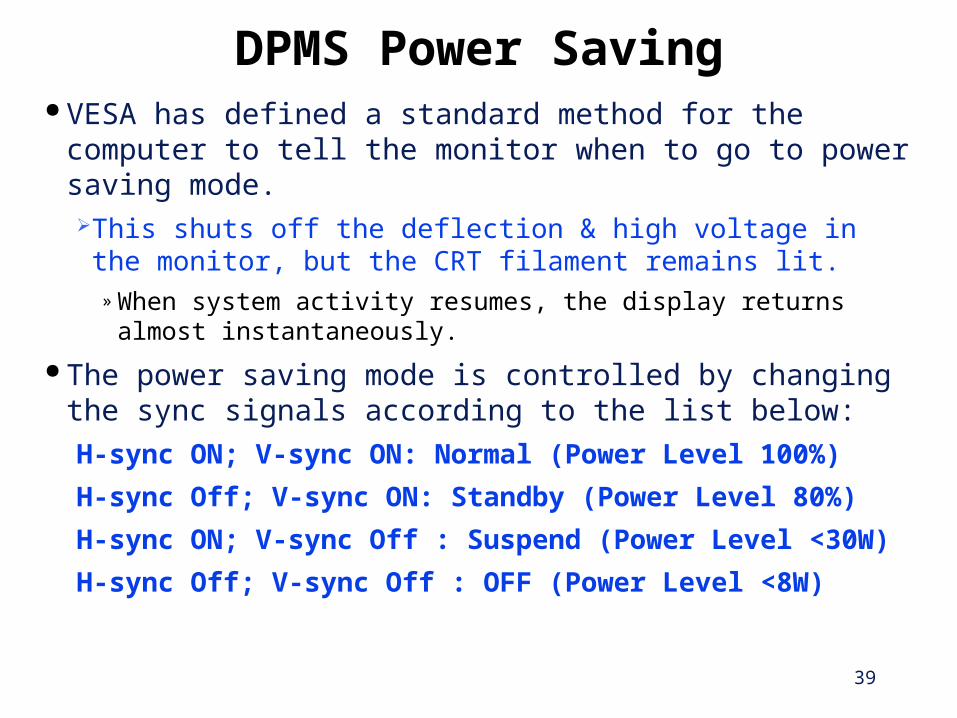
DPMS Power Saving VESA has defined a standard method for the
computer to tell the monitor when to go to power saving mode.This shuts off the deflection & high voltage in the
monitor, but the CRT filament remains lit. » When system activity resumes, the display returns almost
instantaneously.
The power saving mode is controlled by changing the sync signals according to the list below:
H-sync ON; V-sync ON: Normal (Power Level 100%)
H-sync Off; V-sync ON: Standby (Power Level 80%)
H-sync ON; V-sync Off : Suspend (Power Level <30W)
H-sync Off; V-sync Off : OFF (Power Level <8W)
40
REVIEW & SUMMARYWE HAVE DISCUSSED THE FOLLOWING:
The interactions in a Graphics SystemThe PC Video Graphics Controller is responsible for
producing the image that is displayed on the screen.An O/S and/or Application updates screen information
the using the Video BIOS and/or a Video Device Driver.The PC Video Subsystem contains a block of dedicated
Display Memory that holds the text or graphics information to be displayed on the screen.
The VGA Controller serializes the data in it’s display memory and mixes this stream of data with synchronizing signals that control the video display.
41
REVIEW & SUMMARY How images are displayed on a CRT
The rear part of the CRT contains a cathode that emits an electron beam when heated and the front surface of a computer monitor is actually the end of a large CRT.
The CRT’s electron beam sweeps across the screen in a fixed path from left to right and top to bottom.
» The CRT image must be redrawn continuously because it will remain visible for only a few milliseconds depending on the persistence of the phosphor.
In an interlaced graphics system, it takes 2 fields (1 odd, 1 even) to display one complete screen (called a frame).
A non-interlaced display has an entire frame displayed each screen refresh--every line is updated every frame.
42
REVIEW & SUMMARY
Video Subsystem port connectors (15 pin connector )Sync signals are TTL levelThe DAC outputs analog Red, Green, & Blue Video signals to
the monitor guns.
Clock
SYNTH
Horizontal TimingVertical Timing
Dot Stream To Monitor
CRTCRT Ctlr&
Memory Sequencer
Optional
FIFO
VideoMemory
GraphicsController
Attribute Controller
(Palette)
SystemBus
Interface
Control AddrData
Addr Data
Addr
Ctrl
FeatureConnector
Dot Clock
MemClock
DAC(Lookup Table)
R
G
B
A block diagram of the Video Subsystem
Basic elements usually implemented in an ASIC.
Point & Shoot is used to access registers.
End of Chapter 3-1