1 MOS Field-Effect Transistors (MOSFETs). Copyright 2004 by Oxford University Press, Inc....
110
1 MOS Field-Effect Transistors (MOSFETs)
-
Upload
khalil-coey -
Category
Documents
-
view
225 -
download
1
Transcript of 1 MOS Field-Effect Transistors (MOSFETs). Copyright 2004 by Oxford University Press, Inc....

1
MOS Field-EffectTransistors (MOSFETs)

Microelectronic Circuits - Fifth Edition Sedra/Smith 2Copyright 2004 by Oxford University Press, Inc.
Figure 4.1 Physical structure of the enhancement-type NMOS transistor: (a) perspective view; (b) cross-section. Typically L = 0.1 to 3 m, W = 0.2 to 100 m, and the thickness of the oxide layer (tox) is in the range of 2 to 50 nm.

Microelectronic Circuits - Fifth Edition Sedra/Smith 3Copyright 2004 by Oxford University Press, Inc.
Figure 4.2 The enhancement-type NMOS transistor with a positive voltage applied to the gate. An n channel is induced at the top of the substrate beneath the gate.

Microelectronic Circuits - Fifth Edition Sedra/Smith 4Copyright 2004 by Oxford University Press, Inc.
Figure 4.3 An NMOS transistor with vGS > Vt and with a small vDS applied. The device acts as a resistance whose value is determined by vGS. Specifically, the channel conductance is proportional to vGS – Vt’ and thus iD is proportional to (vGS – Vt) vDS. Note that the depletion region is not shown (for simplicity).

Microelectronic Circuits - Fifth Edition Sedra/Smith 5Copyright 2004 by Oxford University Press, Inc.
Figure 4.4 The iD–vDS characteristics of the MOSFET in Fig. 4.3 when the voltage applied between drain and source, vDS, is kept small. The device operates as a linear resistor whose value is controlled by vGS.

Microelectronic Circuits - Fifth Edition Sedra/Smith 6Copyright 2004 by Oxford University Press, Inc.
Figure 4.5 Operation of the enhancement NMOS transistor as vDS is increased. The induced channel acquires a tapered shape, and its resistance increases as vDS is increased. Here, vGS is kept constant at a value > Vt.

Microelectronic Circuits - Fifth Edition Sedra/Smith 7Copyright 2004 by Oxford University Press, Inc.
Figure 4.6 The drain current iD versus the drain-to-source voltage vDS for an enhancement-type NMOS transistor operated with vGS > Vt.

Microelectronic Circuits - Fifth Edition Sedra/Smith 8Copyright 2004 by Oxford University Press, Inc.
Figure 4.7 Increasing vDS causes the channel to acquire a tapered shape. Eventually, as vDS reaches vGS – Vt’ the channel is pinched off at the drain end. Increasing vDS above vGS – Vt has little effect (theoretically, no effect) on the channel’s shape.

Microelectronic Circuits - Fifth Edition Sedra/Smith 9Copyright 2004 by Oxford University Press, Inc.
Figure 4.8 Derivation of the iD–vDS characteristic of the NMOS transistor.
Microelectronic Circuits - Fifth Edition Sedra/Smith 10Copyright 2004 by Oxford University Press, Inc.
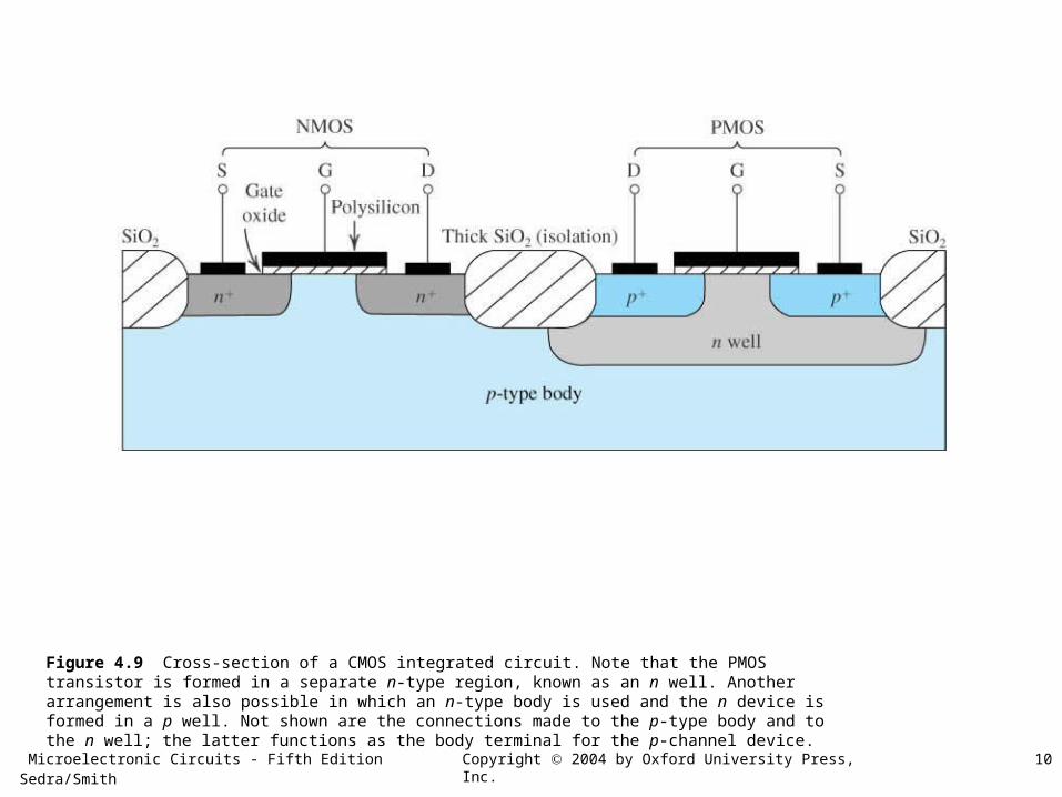
Figure 4.9 Cross-section of a CMOS integrated circuit. Note that the PMOS transistor is formed in a separate n-type region, known as an n well. Another arrangement is also possible in which an n-type body is used and the n device is formed in a p well. Not shown are the connections made to the p-type body and to the n well; the latter functions as the body terminal for the p-channel device.

Microelectronic Circuits - Fifth Edition Sedra/Smith 11Copyright 2004 by Oxford University Press, Inc.
Figure 4.10 (a) Circuit symbol for the n-channel enhancement-type MOSFET. (b) Modified circuit symbol with an arrowhead on the source terminal to distinguish it from the drain and to indicate device polarity (i.e., n channel). (c) Simplified circuit symbol to be used when the source is connected to the body or when the effect of the body on device operation is unimportant.

Microelectronic Circuits - Fifth Edition Sedra/Smith 12Copyright 2004 by Oxford University Press, Inc.
Figure 4.11 (a) An n-channel enhancement-type MOSFET with vGS and vDS applied and with the normal directions of current flow indicated. (b) The iD–vDS characteristics for a device with k’n (W/L) = 1.0 mA/V2.

Microelectronic Circuits - Fifth Edition Sedra/Smith 13Copyright 2004 by Oxford University Press, Inc.
Figure 4.12 The iD–vGS characteristic for an enhancement-type NMOS transistor in saturation (Vt = 1 V, k’n W/L = 1.0 mA/V2).

Microelectronic Circuits - Fifth Edition Sedra/Smith 14Copyright 2004 by Oxford University Press, Inc.
Figure 4.13 Large-signal equivalent-circuit model of an n-channel MOSFET operating in the saturation region.

Microelectronic Circuits - Fifth Edition Sedra/Smith 15Copyright 2004 by Oxford University Press, Inc.
Figure 4.14 The relative levels of the terminal voltages of the enhancement NMOS transistor for operation in the triode region and in the saturation region.

Microelectronic Circuits - Fifth Edition Sedra/Smith 16Copyright 2004 by Oxford University Press, Inc.
Figure 4.15 Increasing vDS beyond vDSsat causes the channel pinch-off point to move slightly away from the drain, thus reducing the effective channel length (by DL).

Microelectronic Circuits - Fifth Edition Sedra/Smith 17Copyright 2004 by Oxford University Press, Inc.
Figure 4.16 Effect of vDS on iD in the saturation region. The MOSFET parameter VA depends on the process technology and, for a given process, is proportional to the channel length L.

Microelectronic Circuits - Fifth Edition Sedra/Smith 18Copyright 2004 by Oxford University Press, Inc.
Figure 4.17 Large-signal equivalent circuit model of the n-channel MOSFET in saturation, incorporating the output resistance ro. The output resistance models the linear dependence of iD on vDS and is given by Eq. (4.22).

Microelectronic Circuits - Fifth Edition Sedra/Smith 19Copyright 2004 by Oxford University Press, Inc.
Figure 4.18 (a) Circuit symbol for the p-channel enhancement-type MOSFET. (b) Modified symbol with an arrowhead on the source lead. (c) Simplified circuit symbol for the case where the source is connected to the body. (d) The MOSFET with voltages applied and the directions of current flow indicated. Note that vGS and vDS are negative and iD flows out of the drain terminal.

Microelectronic Circuits - Fifth Edition Sedra/Smith 20Copyright 2004 by Oxford University Press, Inc.
Figure 4.19 The relative levels of the terminal voltages of the enhancement-type PMOS transistor for operation in the triode region and in the saturation region.
Microelectronic Circuits - Fifth Edition Sedra/Smith 21Copyright 2004 by Oxford University Press, Inc.
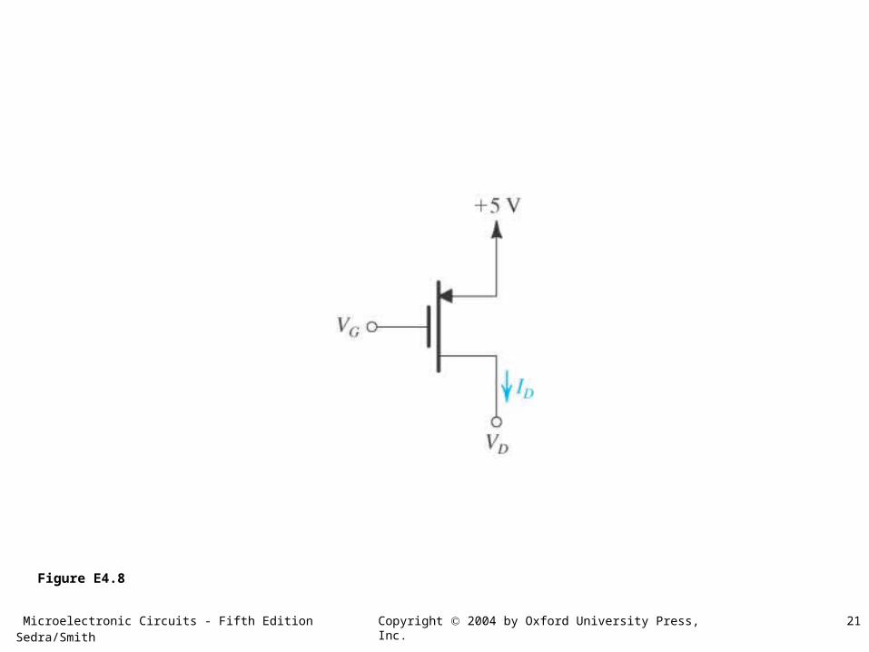
Figure E4.8

Microelectronic Circuits - Fifth Edition Sedra/Smith 22Copyright 2004 by Oxford University Press, Inc.
Table 4.1

Microelectronic Circuits - Fifth Edition Sedra/Smith 23Copyright 2004 by Oxford University Press, Inc.
Figure 4.20 Circuit for Example 4.2.

Microelectronic Circuits - Fifth Edition Sedra/Smith 24Copyright 2004 by Oxford University Press, Inc.
Figure 4.21 Circuit for Example 4.3.
Microelectronic Circuits - Fifth Edition Sedra/Smith 25Copyright 2004 by Oxford University Press, Inc.
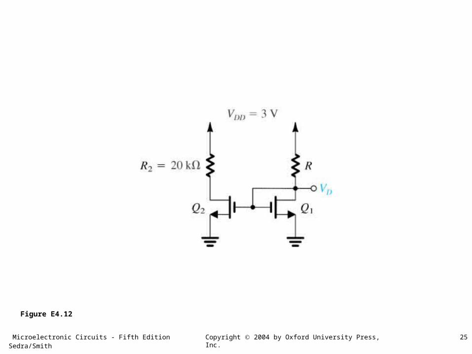
Figure E4.12

Microelectronic Circuits - Fifth Edition Sedra/Smith 26Copyright 2004 by Oxford University Press, Inc.
Figure 4.22 Circuit for Example 4.4.

Microelectronic Circuits - Fifth Edition Sedra/Smith 27Copyright 2004 by Oxford University Press, Inc.
Figure 4.23 (a) Circuit for Example 4.5. (b) The circuit with some of the analysis details shown.

Microelectronic Circuits - Fifth Edition Sedra/Smith 28Copyright 2004 by Oxford University Press, Inc.
Figure 4.24 Circuit for Example 4.6.

Microelectronic Circuits - Fifth Edition Sedra/Smith 29Copyright 2004 by Oxford University Press, Inc.
Figure 4.25 Circuits for Example 4.7.

Microelectronic Circuits - Fifth Edition Sedra/Smith 30Copyright 2004 by Oxford University Press, Inc.
Figure E4.16

Microelectronic Circuits - Fifth Edition Sedra/Smith 31Copyright 2004 by Oxford University Press, Inc.
Figure 4.26 (a) Basic structure of the common-source amplifier. (b) Graphical construction to determine the transfer characteristic of the amplifier in (a).

Microelectronic Circuits - Fifth Edition Sedra/Smith 32Copyright 2004 by Oxford University Press, Inc.
Figure 4.26 (Continued) (c) Transfer characteristic showing operation as an amplifier biased at point Q.

Microelectronic Circuits - Fifth Edition Sedra/Smith 33Copyright 2004 by Oxford University Press, Inc.
Figure 4.27 Two load lines and corresponding bias points. Bias point Q1 does not leave sufficient room for positive signal swing at the drain (too close to VDD). Bias point Q2 is too close to the boundary of the triode region and might not allow for sufficient negative signal swing.

Microelectronic Circuits - Fifth Edition Sedra/Smith 34Copyright 2004 by Oxford University Press, Inc.
Figure 4.28 Example 4.8.

Microelectronic Circuits - Fifth Edition Sedra/Smith 35Copyright 2004 by Oxford University Press, Inc.
Figure 4.28 (Continued)

Microelectronic Circuits - Fifth Edition Sedra/Smith 36Copyright 2004 by Oxford University Press, Inc.
Figure 4.29 The use of fixed bias (constant VGS) can result in a large variability in the value of ID. Devices 1 and 2 represent extremes among units of the same type.

Microelectronic Circuits - Fifth Edition Sedra/Smith 37Copyright 2004 by Oxford University Press, Inc.
Figure 4.30 Biasing using a fixed voltage at the gate, VG, and a resistance in the source lead, RS: (a) basic arrangement; (b) reduced variability in ID; (c) practical implementation using a single supply; (d) coupling of a signal source to the gate using a capacitor CC1; (e) practical implementation using two supplies.

Microelectronic Circuits - Fifth Edition Sedra/Smith 38Copyright 2004 by Oxford University Press, Inc.
Figure 4.31 Circuit for Example 4.9.

Microelectronic Circuits - Fifth Edition Sedra/Smith 39Copyright 2004 by Oxford University Press, Inc.
Figure 4.32 Biasing the MOSFET using a large drain-to-gate feedback resistance, RG.

Microelectronic Circuits - Fifth Edition Sedra/Smith 40Copyright 2004 by Oxford University Press, Inc.
Figure 4.33 (a) Biasing the MOSFET using a constant-current source I. (b) Implementation of the constant-current source I using a current mirror.
Microelectronic Circuits - Fifth Edition Sedra/Smith 41Copyright 2004 by Oxford University Press, Inc.
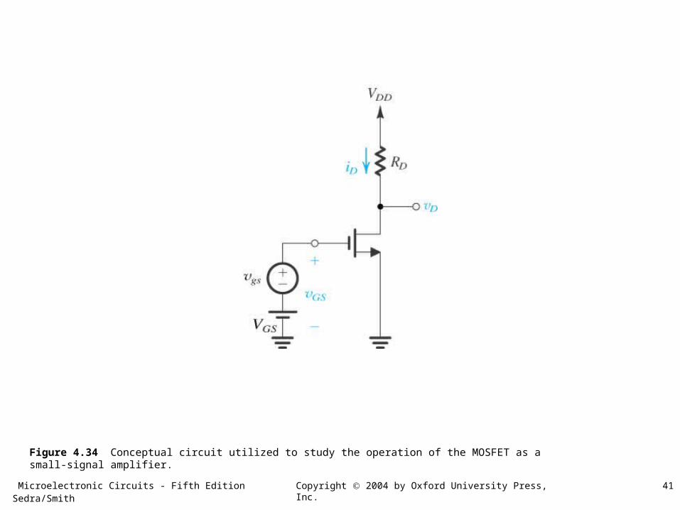
Figure 4.34 Conceptual circuit utilized to study the operation of the MOSFET as a small-signal amplifier.

Microelectronic Circuits - Fifth Edition Sedra/Smith 42Copyright 2004 by Oxford University Press, Inc.
Figure 4.35 Small-signal operation of the enhancement MOSFET amplifier.

Microelectronic Circuits - Fifth Edition Sedra/Smith 43Copyright 2004 by Oxford University Press, Inc.
Figure 4.36 Total instantaneous voltages vGS and vD for the circuit in Fig. 4.34.

Microelectronic Circuits - Fifth Edition Sedra/Smith 44Copyright 2004 by Oxford University Press, Inc.
Figure 4.37 Small-signal models for the MOSFET: (a) neglecting the dependence of iD on vDS in saturation (the channel-length modulation effect); and (b) including the effect of channel-length modulation, modeled by output resistance ro = |VA| /ID.

Microelectronic Circuits - Fifth Edition Sedra/Smith 45Copyright 2004 by Oxford University Press, Inc.
Figure 4.38 Example 4.10: (a) amplifier circuit; (b) equivalent-circuit model.

Microelectronic Circuits - Fifth Edition Sedra/Smith 46Copyright 2004 by Oxford University Press, Inc.
Figure 4.39 Development of the T equivalent-circuit model for the MOSFET. For simplicity, ro has been omitted but can be added between D and S in the T model of (d).

Microelectronic Circuits - Fifth Edition Sedra/Smith 47Copyright 2004 by Oxford University Press, Inc.
Figure 4.40 (a) The T model of the MOSFET augmented with the drain-to-source resistance ro. (b) An alternative representation of the T model.

Microelectronic Circuits - Fifth Edition Sedra/Smith 48Copyright 2004 by Oxford University Press, Inc.
Figure 4.41 Small-signal equivalent-circuit model of a MOSFET in which the source is not connected to the body.

Microelectronic Circuits - Fifth Edition Sedra/Smith 49Copyright 2004 by Oxford University Press, Inc.
Table 4.2

Microelectronic Circuits - Fifth Edition Sedra/Smith 50Copyright 2004 by Oxford University Press, Inc.
Figure 4.42 Basic structure of the circuit used to realize single-stage discrete-circuit MOS amplifier configurations.

Microelectronic Circuits - Fifth Edition Sedra/Smith 51Copyright 2004 by Oxford University Press, Inc.
Figure E4.30

Microelectronic Circuits - Fifth Edition Sedra/Smith 52Copyright 2004 by Oxford University Press, Inc.
Table 4.3

Microelectronic Circuits - Fifth Edition Sedra/Smith 53Copyright 2004 by Oxford University Press, Inc.
Figure 4.43 (a) Common-source amplifier based on the circuit of Fig. 4.42. (b) Equivalent circuit of the amplifier for small-signal analysis. (c) Small-signal analysis performed directly on the amplifier circuit with the MOSFET model implicitly utilized.

Microelectronic Circuits - Fifth Edition Sedra/Smith 54Copyright 2004 by Oxford University Press, Inc.
Figure 4.44 (a) Common-source amplifier with a resistance RS in the source lead. (b) Small-signal equivalent circuit with ro neglected.

Microelectronic Circuits - Fifth Edition Sedra/Smith 55Copyright 2004 by Oxford University Press, Inc.
Figure 4.45 (a) A common-gate amplifier based on the circuit of Fig. 4.42. (b) A small-signal equivalent circuit of the amplifier in (a). (c) The common-gate amplifier fed with a current-signal input.

Microelectronic Circuits - Fifth Edition Sedra/Smith 56Copyright 2004 by Oxford University Press, Inc.
Figure 4.46 (a) A common-drain or source-follower amplifier. (b) Small-signal equivalent-circuit model. (c) Small-signal analysis performed directly on the circuit. (d) Circuit for determining the output resistance Rout of the source follower.

Microelectronic Circuits - Fifth Edition Sedra/Smith 57Copyright 2004 by Oxford University Press, Inc.
Table 4.4

Microelectronic Circuits - Fifth Edition Sedra/Smith 58Copyright 2004 by Oxford University Press, Inc.
Table 4.4 (Continued)

Microelectronic Circuits - Fifth Edition Sedra/Smith 59Copyright 2004 by Oxford University Press, Inc.
Figure 4.47 (a) High-frequency equivalent circuit model for the MOSFET. (b) The equivalent circuit for the case in which the source is connected to the substrate (body). (c) The equivalent circuit model of (b) with Cdb neglected (to simplify analysis).

Microelectronic Circuits - Fifth Edition Sedra/Smith 60Copyright 2004 by Oxford University Press, Inc.
Figure 4.48 Determining the short-circuit current gain Io /Ii.

Microelectronic Circuits - Fifth Edition Sedra/Smith 61Copyright 2004 by Oxford University Press, Inc.
Table 4.5

Microelectronic Circuits - Fifth Edition Sedra/Smith 62Copyright 2004 by Oxford University Press, Inc.
Figure 4.49 (a) Capacitively coupled common-source amplifier. (b) A sketch of the frequency response of the amplifier in (a) delineating the three frequency bands of interest.

Microelectronic Circuits - Fifth Edition Sedra/Smith 63Copyright 2004 by Oxford University Press, Inc.
Figure 4.50 Determining the high-frequency response of the CS amplifier: (a) equivalent circuit; (b) the circuit of (a) simplified at the input and the output;

Microelectronic Circuits - Fifth Edition Sedra/Smith 64Copyright 2004 by Oxford University Press, Inc.
Figure 4.50 (Continued) (c) the equivalent circuit with Cgd replaced at the input side with the equivalent capacitance Ceq; (d) the frequency response plot, which is that of a low-pass single-time-constant circuit.

Microelectronic Circuits - Fifth Edition Sedra/Smith 65Copyright 2004 by Oxford University Press, Inc.
Figure 4.51 Analysis of the CS amplifier to determine its low-frequency transfer function. For simplicity, ro is neglected.

Microelectronic Circuits - Fifth Edition Sedra/Smith 66Copyright 2004 by Oxford University Press, Inc.
Figure 4.52 Sketch of the low-frequency magnitude response of a CS amplifier for which the three break frequencies are sufficiently separated for their effects to appear distinct.

Microelectronic Circuits - Fifth Edition Sedra/Smith 67Copyright 2004 by Oxford University Press, Inc.
Figure 4.53 The CMOS inverter.

Microelectronic Circuits - Fifth Edition Sedra/Smith 68Copyright 2004 by Oxford University Press, Inc.
Figure 4.54 Operation of the CMOS inverter when vI is high: (a) circuit with vI = VDD (logic-1 level, or VOH); (b) graphical construction to determine the operating point; (c) equivalent circuit.

Microelectronic Circuits - Fifth Edition Sedra/Smith 69Copyright 2004 by Oxford University Press, Inc.
Figure 4.55 Operation of the CMOS inverter when vI is low: (a) circuit with vI = 0 V (logic-0 level, or VOL); (b) graphical construction to determine the operating point; (c) equivalent circuit.

Microelectronic Circuits - Fifth Edition Sedra/Smith 70Copyright 2004 by Oxford University Press, Inc.
Figure 4.56 The voltage transfer characteristic of the CMOS inverter.
Microelectronic Circuits - Fifth Edition Sedra/Smith 71Copyright 2004 by Oxford University Press, Inc.
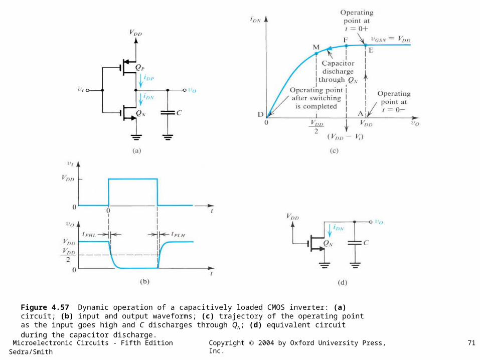
Figure 4.57 Dynamic operation of a capacitively loaded CMOS inverter: (a) circuit; (b) input and output waveforms; (c) trajectory of the operating point as the input goes high and C discharges through QN; (d) equivalent circuit during the capacitor discharge.

Microelectronic Circuits - Fifth Edition Sedra/Smith 72Copyright 2004 by Oxford University Press, Inc.
Figure 4.58 The current in the CMOS inverter versus the input voltage.

Microelectronic Circuits - Fifth Edition Sedra/Smith 73Copyright 2004 by Oxford University Press, Inc.
Figure 4.59 (a) Circuit symbol for the n-channel depletion-type MOSFET. (b) Simplified circuit symbol applicable for the case the substrate (B) is connected to the source (S).
Microelectronic Circuits - Fifth Edition Sedra/Smith 74Copyright 2004 by Oxford University Press, Inc.
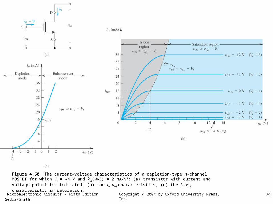
Figure 4.60 The current-voltage characteristics of a depletion-type n-channel MOSFET for which Vt = –4 V and kn(W/L)
= 2 mA/V2: (a) transistor with current and voltage polarities indicated; (b) the iD–vDS characteristics; (c) the iD–vGS characteristic in saturation.
Microelectronic Circuits - Fifth Edition Sedra/Smith 75Copyright 2004 by Oxford University Press, Inc.
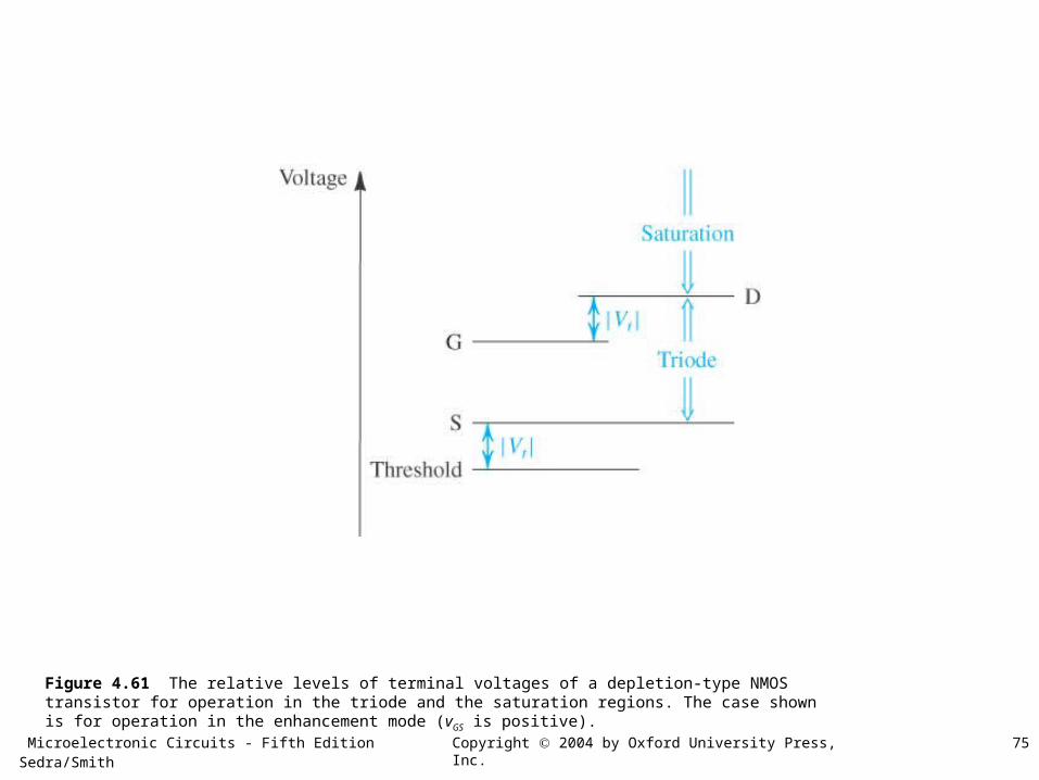
Figure 4.61 The relative levels of terminal voltages of a depletion-type NMOS transistor for operation in the triode and the saturation regions. The case shown is for operation in the enhancement mode (vGS is positive).

Microelectronic Circuits - Fifth Edition Sedra/Smith 76Copyright 2004 by Oxford University Press, Inc.
Figure 4.62 Sketches of the iD–vGS characteristics for MOSFETs of enhancement and depletion types, of both polarities (operating in saturation). Note that the characteristic curves intersect the vGS axis at Vt. Also note that for generality somewhat different values of |Vt| are shown for n-channel and p-channel devices.

Microelectronic Circuits - Fifth Edition Sedra/Smith 77Copyright 2004 by Oxford University Press, Inc.
Figure E4.51

Microelectronic Circuits - Fifth Edition Sedra/Smith 78Copyright 2004 by Oxford University Press, Inc.
Figure E4.52

Microelectronic Circuits - Fifth Edition Sedra/Smith 79Copyright 2004 by Oxford University Press, Inc.
Figure 4.63 Capture schematic of the CS amplifier in Example 4.14.

Microelectronic Circuits - Fifth Edition Sedra/Smith 80Copyright 2004 by Oxford University Press, Inc.
Figure 4.64 Frequency response of the CS amplifier in Example 4.14 with CS = 10 F and CS = 0 (i.e., CS removed).

Microelectronic Circuits - Fifth Edition Sedra/Smith 81Copyright 2004 by Oxford University Press, Inc.
Figure P4.18

Microelectronic Circuits - Fifth Edition Sedra/Smith 82Copyright 2004 by Oxford University Press, Inc.
Figure P4.33

Microelectronic Circuits - Fifth Edition Sedra/Smith 83Copyright 2004 by Oxford University Press, Inc.
Figure P4.36

Microelectronic Circuits - Fifth Edition Sedra/Smith 84Copyright 2004 by Oxford University Press, Inc.
Figure P4.37

Microelectronic Circuits - Fifth Edition Sedra/Smith 85Copyright 2004 by Oxford University Press, Inc.
Figure P4.38

Microelectronic Circuits - Fifth Edition Sedra/Smith 86Copyright 2004 by Oxford University Press, Inc.
Figure P4.41

Microelectronic Circuits - Fifth Edition Sedra/Smith 87Copyright 2004 by Oxford University Press, Inc.
Figure P4.42

Microelectronic Circuits - Fifth Edition Sedra/Smith 88Copyright 2004 by Oxford University Press, Inc.
Figure P4.43

Microelectronic Circuits - Fifth Edition Sedra/Smith 89Copyright 2004 by Oxford University Press, Inc.
Figure P4.44
Microelectronic Circuits - Fifth Edition Sedra/Smith 90Copyright 2004 by Oxford University Press, Inc.
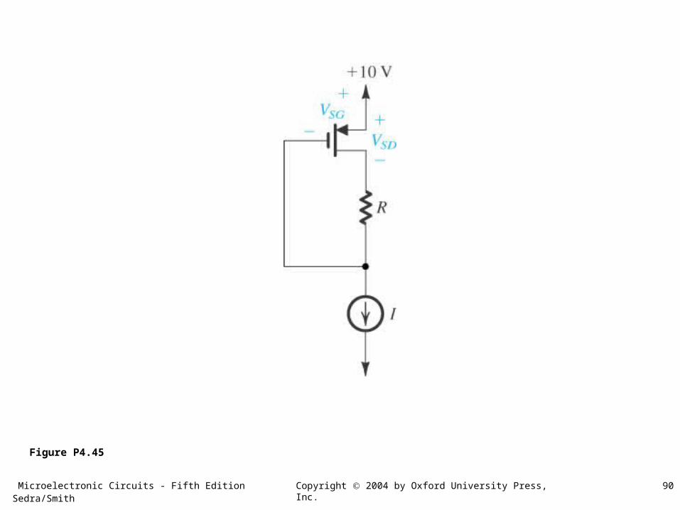
Figure P4.45

Microelectronic Circuits - Fifth Edition Sedra/Smith 91Copyright 2004 by Oxford University Press, Inc.
Figure P4.46

Microelectronic Circuits - Fifth Edition Sedra/Smith 92Copyright 2004 by Oxford University Press, Inc.
Figure P4.47

Microelectronic Circuits - Fifth Edition Sedra/Smith 93Copyright 2004 by Oxford University Press, Inc.
Figure P4.48

Microelectronic Circuits - Fifth Edition Sedra/Smith 94Copyright 2004 by Oxford University Press, Inc.
Figure P4.54

Microelectronic Circuits - Fifth Edition Sedra/Smith 95Copyright 2004 by Oxford University Press, Inc.
Figure P4.61

Microelectronic Circuits - Fifth Edition Sedra/Smith 96Copyright 2004 by Oxford University Press, Inc.
Figure P4.66

Microelectronic Circuits - Fifth Edition Sedra/Smith 97Copyright 2004 by Oxford University Press, Inc.
Figure P4.74

Microelectronic Circuits - Fifth Edition Sedra/Smith 98Copyright 2004 by Oxford University Press, Inc.
Figure P4.75

Microelectronic Circuits - Fifth Edition Sedra/Smith 99Copyright 2004 by Oxford University Press, Inc.
Figure P4.77
Microelectronic Circuits - Fifth Edition Sedra/Smith 100Copyright 2004 by Oxford University Press, Inc.
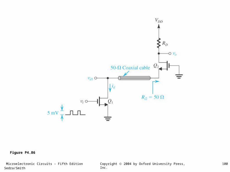
Figure P4.86

Microelectronic Circuits - Fifth Edition Sedra/Smith 101Copyright 2004 by Oxford University Press, Inc.
Figure P4.87
Microelectronic Circuits - Fifth Edition Sedra/Smith 102Copyright 2004 by Oxford University Press, Inc.
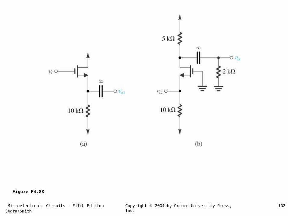
Figure P4.88

Microelectronic Circuits - Fifth Edition Sedra/Smith 103Copyright 2004 by Oxford University Press, Inc.
Figure P4.97

Microelectronic Circuits - Fifth Edition Sedra/Smith 104Copyright 2004 by Oxford University Press, Inc.
Figure P4.99

Microelectronic Circuits - Fifth Edition Sedra/Smith 105Copyright 2004 by Oxford University Press, Inc.
Figure P4.101

Microelectronic Circuits - Fifth Edition Sedra/Smith 106Copyright 2004 by Oxford University Press, Inc.
Figure P4.104

Microelectronic Circuits - Fifth Edition Sedra/Smith 107Copyright 2004 by Oxford University Press, Inc.
Figure P4.117

Microelectronic Circuits - Fifth Edition Sedra/Smith 108Copyright 2004 by Oxford University Press, Inc.
Figure P4.120

Microelectronic Circuits - Fifth Edition Sedra/Smith 109Copyright 2004 by Oxford University Press, Inc.
Figure P4.121

Microelectronic Circuits - Fifth Edition Sedra/Smith 110Copyright 2004 by Oxford University Press, Inc.
Figure P4.123