
1 INTRODUCTION IJSER · PDF filedevelop complex VLSI circuits using CNTFETs. The VI...
9
International Journal of Scientific & Engineering Research, Volume 4, Issue 7, July-2013 1906 ISSN 2229-5518 IJSER © 2013 http://www.ijser.org Modelling and Characterization of CNTFET using Hspice Y.Maheswar, Dr.B.L.Raju, Dr.K.Soundara Rajan Abstract— Carbon nanotubes are becoming more and more popular due to its mechanical and electrical properties. Currently CNTFETs have been used for various applications in building VLSI circuits. However, there is very little literature discussing the procedures to use CNTFET for developing VLSI circuits. In this paper we present a novel approach that uses CNTFET models from Stanford University and analysis the electrical properties of CNTFETs using Spice as well as Matlab. The procedure developed in this paper can be used to develop complex VLSI circuits using CNTFETs. The VI characteristics of CNTFET obtained are cross verified with both Spice as well as Matlab models. Index Terms— CNTFET, Spice, Matlab, VI Characteristics, Equivalent Circuit —————————— —————————— 1 INTRODUCTION Carbon nanotubes are promising candidates for passive or active elements in post-CMOS nanoelectronics. Avouris brought experimental evidences that CNTFETs could have better performances than ultimate silicon MOSFETs [1]. Simi- lar results were obtained in the group of H. Dai [2]. For now, many experimental groups are studying CNT based devices, covering various topics: - the influence of the metal used for the contacts to con- trol charge injection efficiency, - their frequency dependent behaviours, - Their new promising functionalities. However, to predict the ultimate performances of these novel nanodevices, and to further offer guidance and cost reduction of the technological development, accurate and reliable simu- lation tools appears as key issues. Indeed, as the micro- electronics companies show an increasing concern with post- CMOS technologies, there is a strong demand for simulation tools. In particular, companies that develop circuit simulation softwares try to include modelling of nanodevices-based cir- cuits in their available products. For CNT devices, as well as for other molecular electronics devices, it is necessary to de- velop new models, since the standard approximations and models used for MOS electronics may lose their applicability range. A first difficulty arises from the fact that intrinsic transport properties of CNTs are much less understood than their bulk semi-conductors counterparts, widely used in mi- croelectronics. The energy band structure strongly depends on the nanotube helicity and radius, and the scattering mecha- nisms (phonons, impurities) have been theoretically evaluated in a reduced number of cases. ----------------------------------------------------------------------------------- • Y.Maheswar is currently pursuing Ph.D in ECE JNT University, INDIA, Ph: 9642359378. E.Mail: [email protected] • Dr.B.LRaju is currently working as principal in AURO- RA Engg college, INDIA, Ph: 9440925929 E.Mail: [email protected] • Dr.K.Soundara rajan is currently working as professor in ECE JNT University, INDIA, Ph: 8897511366 E.Mail: [email protected] A second serious difficulty is the experimentally observed dispersion of device characteristics. This dispersion is general- ly assigned to the variability of metal/nanotube interfaces at the molecular scale. So, to obtain predictive circuit simulation results, it is mandatory to precisely understand transport phe- nomena in CNTFET at the molecular scale. Hence, considering a single walled, semiconducting carbon nanotube as the chan- nel of a CNTFET including source, drain, gate electrodes, the circuit compatible model should describe the transistor one- dimensional (1-D) electrostatics in its ballistic limit of perfor- mance. Moreover, for convenient and efficient circuit simula- tion, the circuit-compatible model has to be suitable for a wide range of CNTFETs diameters ranging from 0.6 to 3 nm and for varied chiralities as long as they are semiconducting. Alt- hough such model derives from required approximations and simplifications to develop analytical expressions, strong foun- dation of the underlying physics of operation [3] determine the accuracy of the circuit transfer (dc) characteristics together with the transient response. There are various reports in the literature discussion about applications of CNTFET, however many of the papers report the CNT characterization. In this work, we discuss the physical structure of CNT, its equivalent circuit, model files and also present an experimental setup to simulate CNTFETs. We also discuss the electrical and VI char- acteristics of CNTFET. Section II describes the carbon nanotube structure and its physical properties. Section III presents the CNT FET model and its equivalent circuit and Section IV presents the simula- tion results of CNTFET model using Hspice as well as Matlab. Section V discusses the conclusion. 2 CARBON NANOTUBE The discovery of carbon nanotubes actually originates from fullerences, a hollow spherical structure of an allotrope of carbon C-60, which was discovered in 1985. The spherical structure is also called buckminster fullerence, or buckyball, named after a noted architect Richard Buckmister. Some of the scientists who discovered this, including Harold Kroto, Robert IJSER
Transcript of 1 INTRODUCTION IJSER · PDF filedevelop complex VLSI circuits using CNTFETs. The VI...

International Journal of Scientific & Engineering Research, Volume 4, Issue 7, July-2013 1906 ISSN 2229-5518
IJSER © 2013 http://www.ijser.org
Modelling and Characterization of CNTFET using Hspice
Y.Maheswar, Dr.B.L.Raju, Dr.K.Soundara Rajan
Abstract— Carbon nanotubes are becoming more and more popular due to its mechanical and electrical properties. Currently CNTFETs have been used for various applications in building VLSI circuits. However, there is very little literature discussing the procedures to use CNTFET for developing VLSI circuits. In this paper we present a novel approach that uses CNTFET models from Stanford University and analysis the electrical properties of CNTFETs using Spice as well as Matlab. The procedure developed in this paper can be used to develop complex VLSI circuits using CNTFETs. The VI characteristics of CNTFET obtained are cross verified with both Spice as well as Matlab models.
Index Terms— CNTFET, Spice, Matlab, VI Characteristics, Equivalent Circuit
—————————— ——————————
1 INTRODUCTION Carbon nanotubes are promising candidates for passive or active elements in post-CMOS nanoelectronics. Avouris brought experimental evidences that CNTFETs could have better performances than ultimate silicon MOSFETs [1]. Simi-lar results were obtained in the group of H. Dai [2]. For now, many experimental groups are studying CNT based devices, covering various topics:
- the influence of the metal used for the contacts to con-trol charge injection efficiency,
- their frequency dependent behaviours, - Their new promising functionalities.
However, to predict the ultimate performances of these novel nanodevices, and to further offer guidance and cost reduction of the technological development, accurate and reliable simu-lation tools appears as key issues. Indeed, as the micro-electronics companies show an increasing concern with post-CMOS technologies, there is a strong demand for simulation tools. In particular, companies that develop circuit simulation softwares try to include modelling of nanodevices-based cir-cuits in their available products. For CNT devices, as well as for other molecular electronics devices, it is necessary to de-velop new models, since the standard approximations and models used for MOS electronics may lose their applicability range. A first difficulty arises from the fact that intrinsic transport properties of CNTs are much less understood than their bulk semi-conductors counterparts, widely used in mi-croelectronics. The energy band structure strongly depends on the nanotube helicity and radius, and the scattering mecha-nisms (phonons, impurities) have been theoretically evaluated in a reduced number of cases. -----------------------------------------------------------------------------------
• Y.Maheswar is currently pursuing Ph.D in ECE JNT University, INDIA, Ph: 9642359378. E.Mail: [email protected]
• Dr.B.LRaju is currently working as principal in AURO-RA Engg college, INDIA, Ph: 9440925929 E.Mail: [email protected]
• Dr.K.Soundara rajan is currently working as professor in ECE JNT University, INDIA, Ph: 8897511366 E.Mail: [email protected]
A second serious difficulty is the experimentally observed dispersion of device characteristics. This dispersion is general-ly assigned to the variability of metal/nanotube interfaces at the molecular scale. So, to obtain predictive circuit simulation results, it is mandatory to precisely understand transport phe-nomena in CNTFET at the molecular scale. Hence, considering a single walled, semiconducting carbon nanotube as the chan-nel of a CNTFET including source, drain, gate electrodes, the circuit compatible model should describe the transistor one-dimensional (1-D) electrostatics in its ballistic limit of perfor-mance. Moreover, for convenient and efficient circuit simula-tion, the circuit-compatible model has to be suitable for a wide range of CNTFETs diameters ranging from 0.6 to 3 nm and for varied chiralities as long as they are semiconducting. Alt-hough such model derives from required approximations and simplifications to develop analytical expressions, strong foun-dation of the underlying physics of operation [3] determine the accuracy of the circuit transfer (dc) characteristics together with the transient response. There are various reports in the literature discussion about applications of CNTFET, however many of the papers report the CNT characterization. In this work, we discuss the physical structure of CNT, its equivalent circuit, model files and also present an experimental setup to simulate CNTFETs. We also discuss the electrical and VI char-acteristics of CNTFET. Section II describes the carbon nanotube structure and its physical properties. Section III presents the CNT FET model and its equivalent circuit and Section IV presents the simula-tion results of CNTFET model using Hspice as well as Matlab. Section V discusses the conclusion.
2 CARBON NANOTUBE The discovery of carbon nanotubes actually originates
from fullerences, a hollow spherical structure of an allotrope of carbon C-60, which was discovered in 1985. The spherical structure is also called buckminster fullerence, or buckyball, named after a noted architect Richard Buckmister. Some of the scientists who discovered this, including Harold Kroto, Robert
IJSER

International Journal of Scientific & Engineering Research, Volume 4, Issue 7, July-2013 1907 ISSN 2229-5518
IJSER © 2013 http://www.ijser.org
Curl and Richard Smalley were awarded the 1996 Nobel Prize in Chemistry [1]. Figure 1 shows the three dimensional view of a C-60 buckyball [2]. CNT’s Unique Structure Carbon nanotubes, an extended structure of a fullerence in length, are composed of ultrathin carbon fiber with nanome-ter-size diameter and micrometer-size length. Figure 2 illus-trates what they look like. Basically, they are sheets of graphite rolled up into a tube. What is so unique about CNT is due to the different electrical and thermal conductivities they exhibit when their hexagonal structures are orientated differently. For instance, armchair, chiral and zig-zag structure allow the CNT to act like metal, semiconductor and insulator, respectively. Therefore, such characteristics have been employed in semi-conductor industries. The difference in orientation can be de-termined by a method of measurement termed chiral vector. Like many other scientific discoveries, CNT was accidentally discovered as a by-product by a Japanese scientist, Sumio Iiji-ma, in the carbon cathode used for the arc-discharging process preparing fullerences [3]. Such process later became one of the techniques to synthesize CNT. In next section, some methods of synthesizing CNT will be discussed. The applications of CNT are not limited to semiconductor industry. Over the years, other applications of CNT have been proposed in areas that range from chemistry, physics, and materials to biology. Synthesis and Purification CNT can be classified into two types: multi-walled CNT (MWCNT) and single-walled CNT (SWCNT). MWCNT was discovered earlier than the latter, which is comprised of 2 to 30 concentric graphitic layers, whose diameter ranges from 10 to 50 nm and more than 10 um in length. SWCNT, on the other hand, is a lot thinner due to its single graphite layer and has diameter from 1.0 to 1.4 nm. Systhesis
The synthesis technique of CNT has been studied ex-tensively and now is being prepared by many methods: arc-discharging, laser ablation and catalytic decomposition of hy-drocarbons. Other methods such as electrolysis and solar en-ergy have been proposed. More effort has been put into the study of the synthesis of SWCNT. However, both MWCNT and SWCNT share some techniques in terms of synthesis. They both require some metals as catalyst, including Fe, Co, Ni. SWCNT requires alloys, such as Fe/Co, Fe/Ni, Ni/Co, Ni/Cu, etc. The following are some of the techniques to syn-thesize CNTs. Electric arc Discharge Two carbon electrodes are kept with a gap in between. When high current, about 80 A is passed through the electrodes where gap is filled with helium under 300 torr. Cylindrical deposit then grows at about 2 to 3 mm per minute. This cath-ode deposit contains two portions: the inside is a black fragile core and the outside a hard shell. Generally, two parameters determine the quantity and the quality of the CNT deposit. Laser Ablation MWCNT synthesized using laser ablation results much short-er in length compared with arc discharge. Surprisingly, the same technique is able to produce SWCNT in excellent high
yield. Therefore, great effort has been put into synthesizing SWCNT using this method.
Fig. 1. A 3-D view of a bucky ball Carbon-60
Fig. 2. Three different orientations of carbon nanotubes in chi-ral vectors
Catalytic Decomposition of Hydrocarbon High quality of MWCNT can be mass produced with this method with lower cost. Metals such as Fe and Ni act as cata-lysts to break down the hydrocarbons passing through quartz tube in gas phase with a heating source. The straightness of the MWCNT produced using this method, however, is not as satisfying as that using arc-discharge. And thus the electrical conductivity is affected. Purification The synthesized CNTs require isolation processes since some nanoparticles, basically the by-products of carbon not in de-sired structure, as well as oxidized carbon, are produced in the synthesis process. Centrifugation, micro-filtration and chro-matography are employed to separate the CNTs of different lengths. 3 DESCRIPTION OF CNTFET A. Carbon nanotube within a transistor configuration
IJSER

International Journal of Scientific & Engineering Research, Volume 4, Issue 7, July-2013 1908 ISSN 2229-5518
IJSER © 2013 http://www.ijser.org
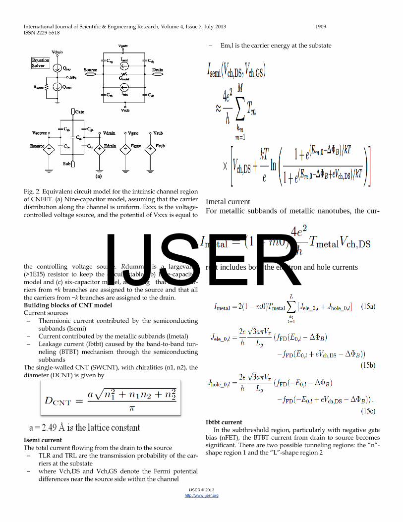
For now, the transistor configurations based on single walled carbon nanotubes (SWNTs) are various: the Schottky barrier CNTFET (SB-CNTFET) [4], the conventional CNTFET (C-CNTFET) featuring a doping profile similar to n-MOSFET [5], the dual-gate CNTFET exhibits n- or p-type unipolar behavior tunable by electrostatic doping [6] and the tunneling CNTFET [7]. The subject of this paper is the conventional CNTFET. Its structure albeit simple provides a behavior like normal MOSFET with yet ballistic transport [8]. A typical layout of a MOSFET-like CNFET device is shown in Fig. 1. The CNT channel region is undoped, whereas the other regions are heavily doped, acting as both the source/drain extension re-gion and/or interconnects between two adjacent devices (un-contacted source–gate/gate–drain configurations). This sec-tion describes the modeling of one single intrinsic channel of CNFET, as shown in Fig. 1 (inset), which is a starting point toward the complete device model reported in [1]. For MOSFET-like CNFET, since positive-FET (pFET) behavior is similar to negative FET (nFET), we only describe the equations for nFET in this paper, although we implemented both nFET and pFET for the SPICE simulations. III. Model of the Intrinsic Channel Region This part models the intrinsic channel region of CNFET with a near-ballistic transport and without any parasitic capacitance and parasitic resistance. The equivalent circuit model is shown as Fig. 2. Fig. 2(a) is the equivalent circuit implemented with HSPICE, and Fig. 2(b) and (c) is the other two possible imple-mentations for the transcapacitance network. The Fermi-level profiles and the energy-band diagram in the channel region with a ballistic transport are shown in Fig. 3(a). The potential differences μs − μ_s and μd − μ_d are determined by both the applied bias and the property of the source/drain extension regions. We will treat the nonballistic transport and the potential drop at the source/drain extension
region and the contacts in the complete device model [1]. Fig. 1. Three-dimensonal device structure of CNFETs with
multiple channels, high-k gate dielectric material, and related parasitic gate capacitances. In this example, three CNFETs are fabricated along one single CNT. The channel region of CNTs is undoped, whereas the other regions of CNTs are heavily doped. The inset shows the 3-D device structure of CNFET that is modeled in this work, with only the intrinsic channel region.
IJSER
International Journal of Scientific & Engineering Research, Volume 4, Issue 7, July-2013 1909 ISSN 2229-5518
IJSER © 2013 http://www.ijser.org
Fig. 2. Equivalent circuit model for the intrinsic channel region of CNFET. (a) Nine-capacitor model, assuming that the carrier distribution along the channel is uniform. Exxx is the voltage-controlled voltage source, and the potential of Vxxx is equal to
the controlling voltage source. Rdummy is a largevalue (>1E15) resistor to keep the circuit stable. (b) Five-capacitor model and (c) six-capacitor model, assuming that all the car-riers from +k branches are assigned to the source and that all the carriers from −k branches are assigned to the drain. Building blocks of CNT model Current sources – Thermionic current contributed by the semiconducting
subbands (Isemi) – Current contributed by the metallic subbands (Imetal) – Leakage current (Ibtbt) caused by the band-to-band tun-
neling (BTBT) mechanism through the semiconducting subbands
The single-walled CNT (SWCNT), with chiralities (n1, n2), the diameter (DCNT) is given by
Isemi current The total current flowing from the drain to the source – TLR and TRL are the transmission probability of the car-
riers at the substate – where Vch,DS and Vch,GS denote the Fermi potential
differences near the source side within the channel
– Em,l is the carrier energy at the substate
Imetal current For metallic subbands of metallic nanotubes, the cur-
rent includes both the electron and hole currents
Ibtbt current
In the subthreshold region, particularly with negative gate bias (nFET), the BTBT current from drain to source becomes significant. There are two possible tunneling regions: the “n”-shape region 1 and the “L”-shape region 2
IJSER

International Journal of Scientific & Engineering Research, Volume 4, Issue 7, July-2013 1910 ISSN 2229-5518
IJSER © 2013 http://www.ijser.org
Trans-capacitance Network To model the intrinsic ac response of CNFET device, a con-trolled transcapacitance array among the four electrodes (G, S,D, andB) with the Meyer capacitor model
CQs and CQd as the quantum capacitance due to the carriers from source (+k branch) and drain (−k branch), respectively The capacitance Csb and Cdb are computed as Csb = Csg · (Csub/Cox) and Cdb = Cdg · (Csub/Cox) The coupling capacitance between the gate and the substrate is derived as
VI characteristics of CNTFET Figure below shows the CNTFET symbol, it consists of source, drain, gate and bulk terminals
The model files for the characteristics of CNTFET are devel-oped by Stanford university which have been obtained and used under license agreement to carry out his experimental work. Stanford CNT model Files Two model variants are available:
– Standard CNFET Model [Recommended] – Uniform-tubes CNFET Model
In the Standard CNFET Model (Standard Model), the nano-tubes in a given device are automatically grouped into two groups: the two CNTs at two ends (with only one neighboring nanotube) and the other n-2 CNTs in between (each with two neighbors to the sides). The Uniform-tubes CNFET Model (Uniform Model) is an approximation to the Standard Model to speed up runtime. The Standard Model is recommended as it is most accurate and fast.
IJSER

International Journal of Scientific & Engineering Research, Volume 4, Issue 7, July-2013 1911 ISSN 2229-5518
IJSER © 2013 http://www.ijser.org
To instantiate the devices in the model, the library must be included at the beginning of the SPICE deck: .lib ‘CNFET.lib’ CNFET This will allow to instantiate any of the following models: NCNFET Standard n-type CNFET model. PCNFET Standard p-type CNFET model. NCNFET_uniform Uniform-tubes n-type CNFET model. PCNFET_uniform Uniform-tubes p-type CNFET model. The model file (PARAMETERS.lib) included in the package is automatically referenced by the top level model files and should not be modified. Results and Discussion: The CNTFET model is included in the spice program as shown below and the results are obtained. An inverter is de-signed and modeled for analysis. Spice Model for CNTFET ******************************************************************** * Carbon Nanotube Field Effect Transistors * Copyright The Board Trustees of the Leland Stanford Junior University 2009 * * Carbon Nanotube Field Effect Transistors Verilog-A im-plementation * based on "A Circuit-Compatible SPICE model for En-
hancement Mode Carbon * Nanotube Field Effect Transistors" by Jie Deng and H-S Philip Wong * File name: cnfet_sample.sp ******************************************************************** ******************************************************************** * LICENSE AGREEMENT * Stanford Leland Junior University and the authors ("Stan-ford") * provide these model files to you subject to the License Agreement, * which may be updated by us from time to time without no-tice to you. * The most-up-to-date License Agreement can be found at * http://nano.stanford.edu/license.php ******************************************************************** .TITLE 'IDS vs VGS for CNFET' .options POST .options AUTOSTOP .options INGOLD=2 DCON=1 .options GSHUNT=1e-12 RMIN=1e-15 .options ABSTOL=1e-5 ABSVDC=1e-4 .options RELTOL=1e-2 RELVDC=1e-2 .options NUMDGT=4 PIVOT=13 .param TEMP=27 .lib 'CNFET.lib' CNFET .param Supply=0.9 .param Vg='Supply' .param Vd='Supply' .param Ccsd=0 CoupleRatio=0 .param m_cnt=1 Efo=0.6 .param Wg=0 Cb=40e-12 .param Lg=32e-9 Lgef=100e-9 .param Vfn=0 Vfp=0 .param m=19 n=0 .param Hox=4e-9 Kox=16 Vdd Drain Gnd Vd Vss Source Gnd 0 Vgg Gate Gnd Vg Vsub Sub Gnd 0 .DC Vgg START=0 STOP='Supply' STEP='0.01*Supply' + SWEEP Vdd START=0 STOP='Supply' STEP='0.1*Supply' *.DC Vgg START=0 STOP='-Supply' STEP='-0.01*Supply' *+ SWEEP Vdd START=0 STOP='-Supply' STEP='-0.1*Supply' .print I(Vdd) .end Spice Model for CNTFET based inverter: .TITLE 'IDS vs VGS for CNFET AND INVERTER DESIGN' .option runlvl=0 .options POST=2 .options AUTOSTOP .options INGOLD=2 DCON=1
IJSER

International Journal of Scientific & Engineering Research, Volume 4, Issue 7, July-2013 1912 ISSN 2229-5518
IJSER © 2013 http://www.ijser.org
.options GSHUNT=1e-12 RMIN=1e-15
.options ABSTOL=1e-5 ABSVDC=1e-4
.options RELTOL=1e-2 RELVDC=1e-2
.options NUMDGT=4 PIVOT=13
.param TEMP=27
.lib 'CNFET.lib' CNFET
.param Supply=1.0 *.param Vg='Supply' .param Vd='Supply' .param Ccsd=0 CoupleRatio=0 .param m_cnt=1 Efo=0.6 .param Wg=0 Cb=40e-12 .param Lg=32e-9 Lgef=100e-9 .param Vfn=0 Vfp=0 .param m=19 n=0 .param Hox=4e-9 Kox=16 *Vdd Vdd gnd dc 1.8v Vdd Vdd Gnd Vd Vss Gnd Gnd 0 *Vgg Gate Gnd Vg Vsub Sub Gnd 0 Vgg Gate Gnd PULSE (0 0.9 0ns 1ns 1ns 25ns 50ns) XPCNFET1 Drain Gate Source Sub PCNFET Lch=Lg Lgeff='Lgef' Lss=32e-9 Ldd=32e-9 + Kgate='Kox' Tox='Hox' Csub='Cb' Vfbp='Vfp' Dout=1 Sout=0 Pitch=20e-9 n1=m n2=n tubes=3 XNCNFET1 Drain Gate Source Sub NCNFET Lch=Lg Lgeff='Lgef' Lss=32e-9 Ldd=32e-9 + Kgate='Kox' Tox='Hox' Csub='Cb' Vfbn='Vfn' Dout=1 Sout=0 Pitch=20e-9 n1=m n2=n tubes=3 *.DC Vgg START=0 STOP='Supply' STEP='0.01*Supply' *+ SWEEP Vdd START=0 STOP='Supply' STEP='0.1*Supply' *.DC Vgg START=0 STOP='-Supply' STEP='-0.01*Supply' *+ SWEEP Vdd START=0 STOP='-Supply' STEP='-0.1*Supply' .print I(Vdd) .plot dc v(Drain) v(Vdd) i(out) .TRAN 1n 200n 50n .plot TRAN v(Gate) v(Vdd) .end
Fig. above shows the drain to source current, ID as a function of the applied gate bias, VGS for the contribution of 1, 2, .., 5 subbands. Once the gate bias exceeds 0,7V, the curves are no more alike, denoting the filling up of the second and more subbands and contributing to the total drain current increase. Note that, when taking into account the three subbands, IDS increases from 40% for VGS=1V compared with the first sub-band. Thus, for this diameter and chirality, the second and third subband contributions are significant. However, as this result is obtained with a low value of the series resistance, this instance corresponds to a future mature technology. There is little difference (< 3%) between the on-current for an infinitely long gate length and the on-current for a 100-nm gate-length device. Thus it is reasonable to assume the ideal device current drive with a gate length longer than 100 nm to be independent of the gate length. With 32-nm gate length, the on-current is about 90% of the long-channel value. With an ideal ballistic transport, the on-current is almost constant with respect to the gate length, except for a slight current drop for short gate lengths (Lg < 100 nm), due to the energy quantization in the axial direction. The on-state current is limited by the amount of charge intro-duced in the channel by the gate and, for source-drain dis-tances shorter than 150nm, the transport is assumed to be free of significant scattering and thus essentially ballistic at both high and low voltages. Hence, the description of current flow through the CNT lies on (i) the features of ballistic transport and (ii) the specific electron confinement along the tube cir-cumference [9]:
Since the current remains constant throughout the channel, the current is calculated at the top of the en-
IJSER

International Journal of Scientific & Engineering Research, Volume 4, Issue 7, July-2013 1913 ISSN 2229-5518
IJSER © 2013 http://www.ijser.org
ergy barrier corresponding to the beginning of the channel.
At the top of the barrier, electrons coming from the source fill up the +k states and the electrons coming from the drain fill up the –k states (Fig. below)).
Depending on the SWNT helicity and radius, the pe-riodic boundary conditions impose restrictions on available states [10], which results in a discrete set of energy subband structure (Fig. below)).
CONCLUSION:
IN THIS WORK, WE HAVE DISCUSSED THE MECHANICAL STRUCTURE
OF CNT AND HAVE ALSO DISCUSSED THE PHYSICAL PROPERTIES OF
CNT BASED ON MECHANICAL STRUCTURE. FURTHER, THE
ELECTRICAL EQUIVALENT OF CNT FET IS DISCUSSED AND AN
EQUIVALENT CIRCUIT IN TERMS OF CURRENT SOURCES, CAPACITANCES AND VOLTAGE SOURCES ARE PRESENTED. A SPICE
MODEL IS USED FROM STANFORD UNIVERSITY TO ANALYZE THE
PERFORMANCES OF SPICE MODEL. THE DEVELOPED PROCEDURE AND
THE SPICE CODE HAVE BEEN USED IN ANALYSIS OF CNTFET MODEL. A SIMPLE INVERTER IS DESIGNED TO CARRY OUT THE ANALYSIS, FROM THE RESULTS OBTAINED THE IMPORTANT PROPERTIES OF
CNTFET HAVE BEEN CAPTURED AND IS ANALYZED. THE
PROCEDURE DISCUSSED CAN BE EXTENDED FOR ANALYSIS OF
CNTFET BASED CIRCUITS.
REFERENCES:
1. PH. AVOURIS, MRS BULL. 29, 403, 2004.
2. A. JAVEY, J. GUO, Q. WANG, M. LUNDSTROM, H. DAI, NATURE 424, PP. 654-657, 2003.
3. S. FREGONESE, G. AVENIER, C. MANEUX, A. CHANTRE, T. ZIMMER, “A COMPACT MODEL FOR HBT ON THIN FILM SOI,” IEEE TRANS. ELEC. DEV., VOL. 53, N° 2, FEB 2006.
4. J. APPENZELLER, J.KNOCH, M. RADOSAVLJEVIC, PH. AVOURIS, “MULTIMODE TRANSPORT IN SCHOTTKY-BARRIER CARBON-NANOTUBE FIELDEFFECT TRANSISTORS,” PHYS. REV. LETT., VOL. 92, N° 22, PP. 226802-1-226802-4 2004.
5. A. RAYCHOWDHURY, S. MUKHOPADHYAY, K. ROY, “A CIRCUIT-COMPATIBLE MODEL OF BALLISTIC CARBON NANOTUBE FIELD-EFFECT TRANSISTORS,” IEEE TRANSACTIONS ON COMPUTER-AIDED DESIGN OF INTEGRATED CIRCUITS AND SYSTEMS, VOL. 23, N° 10, PP. 1411-1420, 2004.
6. YU-MING LIN, J. APPENZELLER, J. KNOCH, PH. AVOURIS, “HIGHPERFORMANCE CARBON NANOTUBE FIELD-EFFECT TRANSISTOR WITH TUNABLE POLARITIES,” IEEE TRANS. ON NANOTECH., VOL. 4, N° 5, 2005.
7. J. APPENZELLER, YU-MING LIN, J. KNOCH, Z. CHENG, PH. AVOURIS, “COMPARING CARBON NANOTUBE TRANSISTORS – THE IDEAL CHOICE : A NOVEL TUNNELLING DEVICE DESIGN,” IEEE TRANS. ELEC. DEV., VOL. 52, N° 12, 2005.
8. S.J. WIND, J. APPENZELLER, PH. AVOURIS, “LATERAL SCALING IN CARBONNANOTUBE FIELD-EFFECT TRANSISTORS,” PHYS. REV. LETT., VOL. 91, N°5, PP. 058301-1-058301-4, AUG. 2003.
9. PH. AVOURIS, J. APPENZELLER, R. MARTEL, S. J. WIND, “CARBON NANOTUBE ELECTRONICS,” PROCEEDINGS OF THE IEEE, VOL. 91, PP. 1772-1784, 2003.
10. R. SAITO, M.S. DRESSELHAUS, G. DRESSELHAUS, PHYSICAL PROPERTIES OF CARBON NANOTUBES (IMPERIAL COLLEGE PRESS, LONDON, 1998).
11. S. DATTA, ELECTRONIC TRANSPORT IN MESOSCOPIC SYSTEMS, CAMBRIDGE STUDIES IN SEMICONDUCTOR PHYSICS AND MICROELECTRONIC ENGINEERING, VOL. 3, CAMBRIDGE UNIVERSITY PRESS, SHAFTESBURY ROAD, CAMBRIDGE, CB2 2RU, 1997.
12. J. DENG AND H.-S. P.WONG, “A COMPACT SPICE MODEL FOR CARBON NANOTUBE FIELD EFFECT TRANSISTORS INCLUDING NON-IDEALITIES AND ITS APPLICATION—PART II: FULL DEVICE MODEL AND CIRCUIT PERFORMANCE BENCHMARKING,” IEEE TRANS.ELECTRON DEVICES, VOL.
IJSER

International Journal of Scientific & Engineering Research, Volume 4, Issue 7, July-2013 1914 ISSN 2229-5518
IJSER © 2013 http://www.ijser.org
54, NO. 12, PP. 3195–3205, DEC. 2007.
13. A. JAVEY, J. GUO, D. B. FARMER, Q. WANG, D. WANG, R. G. GORDON, M. LUNDSTROM, AND H. DAI, “CARBON NANOTUBE FIELD-EFFECT TRANSISTORS WITH INTEGRATED OHMIC CONTACTS AND HIGH-K GATE DIELECTRICS,” NANO LETT., VOL. 4, NO. 3, PP. 447–450, 2004.
14. A. JAVEY, J. GUO, D. B. FARMER, Q. WANG, E. YENILMEZ, R. G. GORDON, M. LUNDSTROM, AND H. DAI, “SELF-ALIGNED BALLISTIC MOLECULAR TRANSISTORS AND ELECTRICALLY PARALLEL NANOTUBE ARRAYS,” NANO LETT., VOL. 4, NO. 7, PP. 1319–1322, 2004.
15. Z. YAO, C. L. KANE, AND C. DEKKER, “HIGH-FIELD ELECTRICAL TRANSPORT IN SINGLE-WALL CARBON NANOTUBES,” PHYS. REV. LETT., VOL. 84, NO. 13, PP. 2941–2944, MAR. 2000.
16. D. MANN, A. JAVEY, J. KONG, Q. WANG, AND H. DAI, “BALLISTIC TRANSPORT IN METALLIC NANOTUBES WITH RELIABLE PD OHMIC CONTACTS,” NANO LETT., VOL. 3, NO. 11, PP. 1541–1544, 2003.
17. Y. CUI, Z. ZHONG, D. WANG, W. U. WANG, AND C. M. LIEBER, “HIGH PERFORMANCE SILICON NANOWIRE FIELD EFFECT TRANSISTORS,” NANO LETT., VOL. 3, NO. 2, PP. 149–152, 2003.
18. K. NATORI, Y. KIMURA, AND T. SHIMIZU, “CHARACTERISTICS OF A CARBON NANOTUBE FIELD-EFFECT TRANSISTOR ANALYZED AS A BALLISTIC NANOWIRE FIELDEFFECT TRANSISTOR,” J. APPL. PHYS., VOL. 97, NO. 3, PP. 034 306.1–034 306.7, 2005.
19. J. GUO, M. LUNDSTROM, AND S. DATTA, “PERFORMANCE PROJECTIONS FOR BALLISTIC CARBON NANOTUBE FIELD-EFFECT TRANSISTORS,” APPL. PHYS. LETT., VOL. 80, NO. 17, PP. 3192–3194, APR. 2002.
20. A. RAYCHOWDHURY, S. MUKHOPADHYAY, AND K. ROY, “A CIRCUIT-COMPATIBLE MODEL OF BALLISTIC CARBON NANOTUBE FIELD-EFFECT TRANSISTORS,” IEEE TRANS. COMPUT.-AIDED DESIGN INTEGR. CIRCUITS SYST., VOL. 23, NO. 10, PP. 1411– 1420, OCT. 2004.
21. C. DWYER, M. CHEUNG, AND D. J. SORIN, “SEMI-EMPIRICAL SPICE MODELS FOR CARBON NANOTUBE FET LOGIC,” IN PROC. 4TH IEEE CONF. NANOTECHNOL.,2004, PP. 386–388.
22. P. J. BURKE, “LÜTTINGER LIQUID THEORY AS A MODEL OF THE GIGAHERTZ ELECTRICAL PROPERTIES OF CARBON NANOTUBES,” IEEE TRANS. NANOTECHNOL., VOL. 1, NO. 3, PP. 129–144, SEP. 2002.
IJSER


![Electronic Detection of Escherichia coli O157︰H7 Using ... · biosensor with treated SWNTs by applying AC dielectrophore-sis [16] method. The CNTFET biosensor was functionalized](https://static.fdocuments.net/doc/165x107/601f5bee23738a7d1815bd76/electronic-detection-of-escherichia-coli-o157ih7-using-biosensor-with-treated.jpg)
