Single stub impedance matching Impedance matching can be ...
Upload
morgan-jenkinsCategory
view
226download
3
1
Impedance Matching
ECE 403
ECE Victoria University of Wellington
Dr Bhujanga ChakrabartiAugust 2015
“RF design is all about impedance matching.”

2
Maximum Power Transfer
Perhaps the most important reason for impedance matching is to maximize the power transfer from a source to a load.
The maximum power transfer from a source to a load occurs when the load impedance is equal to the complex conjugate of the source impedance, or ZL = ZS* .
The +jX component of the source and the −jX component of the load are in series and, thus, cancel each other, leaving only Rs and RL , which are equal by definition. Since Rs and RL are equal, maximum power transfer will occur.

3

4
The primary objective in any impedance matching scheme, is to force a load impedance to “look like” the complex conjugate of the source impedance so that maximum power may be transferred to the load.
This is shown in Fig. 4-3 where a load impedance of 2 − j6 ohms is transformed by the impedance matching network to a value of 5 + j10 ohms. Therefore, the source “sees” a load impedance of 5 + j10 ohms, which just happens to be its complex conjugate.
Because we are dealing with reactances, which are frequency dependent, the perfect impedance match can occur only at one frequency. That is the frequency at which the +jX component exactly equals the −jX component and, thus, cancellation or resonance occurs.
FIG. 4-3. Impedance transformation.

5
L-Networks
FIG. 4-4.The L network.
The component orientation resembles the shape of “L”.
4 possible arrangement with two L and C.
Fig 4.4A and B are in low pass configuration
Fig 4.4C and D are high pass configuration.

6
L-Networks: Z-Matching Example steps
FIG. 4-5. Simple impedance-match network between a 100-ohm source and a 1000-ohmload.
Determine what the load impedance actually looks like when the −j333-ohm capacitor is placed across the 1000-ohm load resistor.
FIG. 4-6.Impedance looking into the parallel combination of RL and X c .

7
Thus, the parallel combination of the −j333-ohm capacitor and the 1000-ohm resistor looks like an impedance of 100 − j300 ohms. This is a series combination of a 100-ohm resistor and −j300-ohm (Fig. 4-7).
FIG. 4-7. Equivalent circuit of Fig. 4-6.
FIG. 4-8. Completing the match.
The addition of the +j300-ohm inductor causes cancellation of the −j300-ohm capacitor leaving only an apparent 100-ohm load resistor. This is shown in Fig. 4-8.

8
L-Network Matching
Now, back to the design of the impedance-matching networks of Fig. 4-4. These circuits can be very easily designed using the following equations:
FIG. 4-9.Summary of the L-network design.
Xp = the shunt reactance,Rs = the series resistance,Xs = the series reactance.
NOTE: Assumed here that RP>R
s.. Otherwise,
we will need to reverse the L-network (design as if the source is load and load is the source).

9
L-Network
The quantities Xp and Xs may be either capacitive or inductive reactance but each must be of the opposite type.
Once Xp is chosen as a capacitor, for example, Xs must be an inductor, and vice versa. See Example 4-1.

10
Example 4.1

11
Example 4.1… contd

12
Complex Loads
1)Absorption: by absorbing stray reactances 2)Resonating: To resonate with any stray reactance with an equal and opposite reactance at the freq of interest
EXAMPLE 4-2
Use the absorption approach to match the source and load shown in Fig. 4-11 (at 100 MHz). Refer example 4.1 results w/o stay X and C.
SolutionIgnore the reactances and simply match
the 100-ohm real part of the source to the 1000-ohm real part of the load (at 100 MHz).
Use a matching network that will place
element inductances in series with stray inductance and element capacitances in
parallel with stray capacitances.
Account for the stray X and C given in Fig. 4.11
FIG. 4-11. Complex source and load circuit for Example 4-2.
We need 4.8 pF of capacitance for the matching at the load end (soln of example 4.1). We already have 2pF. So additional cap reqd =2.8pFAt the source, we need a series 477-nH inductor. We already have a +j126-ohm, or 200-nH, So extra nductance reqd = 477 nH − 200 nH = 277 nH,
FIG. 4-12. Final design circuit for Example 4-2.

13
Example 4.3Design an impedance matching network that will block the flow of DC from the source to the load in Fig. 4-13. The frequency of operation is 75 MHz. Try the resonant approach.
1. Get rid of load side cap, for blocking DC use Fig 4-4C
We have eliminated the stray capacitance (Fig 4.14), we can proceed with matching the network between the 50-ohm source (shown as”load”- error in book, p68) and the apparent 600-ohm load.
Fig. 4-14.
Fig. 4-13.

14
Example 4.3 … contd
FIG. 4-16. Final design circuit for Example 4-3.FIG. 4-15. The circuit of Fig. 4-14 after impedance matching.

15
3- Element MatchingPotential disadvantage of the 2-element L networks.
It is a fact that once Rs and Rp are given, or the source and load impedance, are determined, the Q of the network is defined. In other words, with the L network,the designer does not have a choice of circuit Q and simply must take what he gets.
Remedial measures
The 3-element network overcomes the problem and can be used for narrow-band, high Q applications (Fig 4.17).
Designer can select any practical circuit Q that he wishes as long as it is greater than Q>QL (using L network), I.e QL sets the lower bound of 3-element matching network.
We will consider Pi-networkT network
FIG. 4-17. The three-element Pi network. FIG. 4-18. The three-element T network.
16
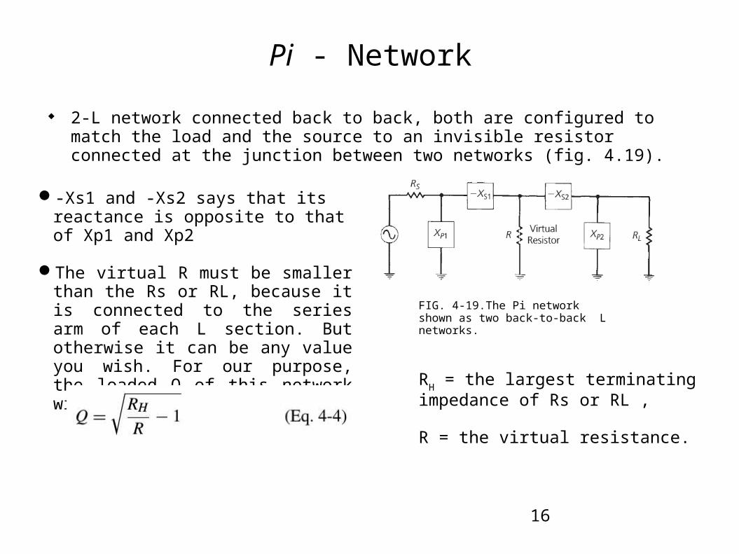
Pi - Network
2-L network connected back to back, both are configured to match the load and the source to an invisible resistor connected at the junction between two networks (fig. 4.19).
FIG. 4-19.The Pi network shown as two back-to-back L networks.
-Xs1 and -Xs2 says that its reactance is opposite to that of Xp1 and Xp2
The virtual R must be smaller than the Rs or RL, because it is connected to the series arm of each L section. But otherwise it can be any value you wish. For our purpose, the loaded Q of this network will be defined by:
RH = the largest terminating
impedance of Rs or RL ,
R = the virtual resistance.

17
Pi- Network ….contd
Any of the networks in Fig. 4-21 can be used for matching between the 100-ohm source and the 1000-ohm load depending on:
The elimination of stray reactances.
The need for harmonic filtering.
The need to pass or block DC voltage.

18
T- Network
You match the load and the source through two L-networks to a virtual resistance.
Vir R > max(Rs, RL)
Eqns 4.4 and 4.5 are the special applications of eqn 4.1
R = the virtual resistance,Rsmall = the smallest terminating resistance.
Rp = the resistance in the shunt branch of the L network,Rs = the resistance in the series branch of the L network.

19
Problem 4.4Using Fig. 4-19 as a reference, design four different Pinetworks to match a 100-ohm source to a 1000-ohm load.Each network must have a loaded Q of 15.
Fig. 4.19
This completes the design of the L section on the load side of the network.
Note that Rseries in the above equation was substituted for the virtual resistor R, which by definition is in the series arm of the L section. The Q for the other L network is now defined by the ratio of Rs to R, as per Equation 4-1.

20
Example 4.4 ...contd
Notice here that the source resistor is now considered to be in the shunt leg of the L network. Therefore, Rs is defined as Rp ,and
note:printing error in the book: The above eqn is for Xs1 not xs2, and also Q1R=(4.6)(4.42)=20.32]. The actual network design is now complete and is shown in Fig. 4-20. Remember that the virtual resistor (R) is not really in the circuit and, therefore, is not shown. Reactances −X s1 and −X s2 are now in series and can simply be added together to form a single component.
Notice that X p1, X s1 , X p2 , and X s2 can all be either capacitive or inductive reactances. The only constraint is that Xp1 and Xs1 are of opposite types, and Xp2 and Xs2 are of opposite types. This yields the four networks of Fig. 4-21 (the source and load have been omitted).
FIG. 4-20. Calculated reactances for Example 4-4.

21
Example 4.4 ...contd
FIG. 4-21. The transformation from double-L to Pi networks.

22
Example 4.5
EXAMPLE 4-5Using Fig. 4-22 as a reference, design four different networks to match a 10-ohm source to a 50-ohm load. Each network is to have a loaded Q of 10.
FIG.4-22. The T network shown as two back-to-back L networks.

23
Example 4.5 ...contd
Using Equation 4-5, we can find the virtual resistance we need for the match.
Now, for the L network on the load end, the Q is defined bythe virtual resistor and the load resistor. Thus

24
Example 4.5 ...contd
The network is now complete and is shown in Fig. 4-23 without the virtual resistor. The two shunt reactances of Fig. 4-23 can again be combinedto form a single element by simply substituting a value that is equal to the combined equivalent parallel reactance of the two.
Fig. 4-23

25
Example 4.5 ...contd
FIG. 4-24. The transformation of circuits from double-L to T-type networks.

26
Smith Chart
We will concentrate mainly on the Smith Chart as an impedance matching tool and other uses will not be covered here.
The mathematical background is as follows.
The reflection coefficient of a load impedance when given a source impedance can be found by the formula:
In normalized form, this equation becomes:
where Zo is a complex impedance of the form R + jX.

27
Smith Chart … contd
Solve Step 5 for X
Substitute step 6 into 5 to get
Step 7 is the equation for a family of circles (Fig 28A) below,whose centers are at:
These are family of constant Resistance circles are shown in Fig 28A.

28
Smith Chart … contd
Radii =
Eliminate R from step 4 and 5 to get
which represents a family of circles with centers at p = 1,q = 1/X, and radii of 1/X. These circles are shown plotted on the p, jq axis in Fig 28B.
FIG. 4-28B. Smith Chart construction.
The arcs of circles shown in Fig. 4-28B are known as constant reactance circles, as each point on a circle has the same reactance as any other point on that circle.

29
SMITH ChartFig. 4-29
http://books.elsevier.com/companions/9780750685184.

30
Plot Z = 1 ±j 1 on Smith chart http://books.elsevier.com/companions/9780750685184.
Fig. 4.30
31
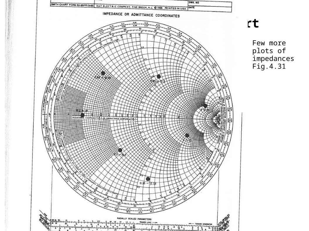
Plot a few Z on Smith chart
Few more plots of impedancesFig.4.31

32
Addition of Series cap of -j1.0 with Z=0.5 +j0.7
Fig 4-32

33
Addition of Series inductor of +j0.8 with Z=0.8-j1
Fig 4-33
For plotting larger Z, Normalise it by dividing with a “Base Z” (say 100) and then plot

34
Conversion of Z to Y and plotting of both
Fig 4-35
Let Z= 1+j1Y=1/Z
Z-Y Graphical relationship is shown in Fig. 4-35

35
Addition of Shunt cap of +j0.8Mho with Y=0.2-j0.5 mho
Parallel admittances are added together
Fig 4-37
Move along constant conductance (G) circle downward (clockwise a distance of +j0.8 mho

36
Addition of Shunt inductor of -j1.5Mho with Y=0.7+j0.5 mho
Parallel admittances are added together
Fig 4-38
Move along constant conductance (G=0.7) circle upward (anti-clockwise) a distance of -j1.5 mho

37
Summary of rotation on Smith chart for series and shunt elements
If we again superimpose the impedance and admittance coordinates and combine Figs. 4-32, 4-33, 4-37, and 4-38 for the general case, we obtain the useful chart shown in Fig. 4-39.
This chart graphically illustrates the direction of travel, along the impedance and admittance coordinates, which results when the particular type of component that is indicated is added to an existing impedance or admittance.
Add Series C Anti-Clock on Z dia
Add shunt C Clock on Y dia
Add Series L Clock on Z dia
Add shunt L Anti-Clock on Y dia

38
Two element matching
To make life much easier for you as a Smith Chart user, thefollowing equations may be used.
For a series-C component:
For a series-L component:
For a shunt-C component:
For a shunt-L component:
ω = 2π f
X = the reactance as read from the chart
B = the susceptance as read from the chart
N = the number used to normalize the original impedances that are to be matched.

39
Example 4.6: Impedance matching on the Smith chart
First, break the circuit down into individual branches asshown in Fig. 4-41. Plot the impedance of the series RLbranch where Z = 1 + j1 ohm. This is point A in Fig. 4-42.Next, following the rules diagrammed in Fig. 4-39, beginadding each component back into the circuit, one at atime. Thus, the following constructions (Fig. 4-42) shouldbe noted:

40
Example 4.6 … contd
The impedance at point E (Fig. 4-42) can then be read directly off of the chart as Z = 0.2 + j0.5 ohm.
Fig 4.42 (prob. 4.6)

41
Example 4.7EXAMPLE 4-7Design a two-element impedance-matching network on a Smith Chart so as to match a 25 − j15-ohm source to a 100 − j25-ohm load at 60 MHz. The matching network must also act as a low-pass filter between the source and the load.
The source wants to “see” a load impedance that is equal to its complex conjugate. Thus, the task before us is to force the 100 − j25-ohm load to look like an impedance of 25 + j15 ohms.
With N=50, Source would like to see an impedance = 0.5 + j0.3 ohm,which is Zs*
Actual load impedance 2 − j0.5 ohms.
These two normalised values are easily plotted on the chart ,Fig.4-44. A=Actual load impedanceC=Complex Conjugate of Source impedance

42
Fig. 4-44:Solution of example 4.7
arc AB of Fig. 4-44 is a shunt cap with a value of +jB = 0.73 mho. The arc BC is a series inductor with a value of +jX = 1.2 ohms.
The shunt capacitor as read from the Smith Chart is a susceptance(B) and can be changed into an equivalent reactance by simply taking the reciprocal.
Example 4.7 ….contd

43
Example 4.7 … contd
The final circuit is shown in Fig. 4-43.
FIG. 4-43. Final circuit for Example 4-7.

44
3-element matching
Representation of Circuit Q on Smith Chart
The Q of a series-impedance circuit is simply equal to the ratio of its reactance to its resistance.
Thus, any point on a Smith Chart has a Q associated with it.
Alternately, if you were to specify a certain Q, you could find an infinite number of points on the chart that could satisfy that Q requirement.
For example, the following impedanceslocated on a Smith Chart have a Q of 5:
Fig. 4-45: Lines of constant Q

45
Procedure for 3-element Z-matching for a specified Q

46

47
Example 4-8 (T network)
EXAMPLE 4-8 Design a T network to match a Z = 15 + j15-ohm source to a 225-ohm load at 30 MHz with a loaded Q of 5.
Draw the arcs for Q = 5 first and, then, plot the load impedance and thecomplex conjugate of the source impedance. ZS* = 0.2- j0.2 ohmsZL=3 ohms
The construction details for the design are shown in Fig. 4-46.
The design statement specifies a T network. Thus, the sourcetermination will determine the network Q because Rs < RL .
Following the procedure for R s < RL (Step 4, above), first plotpoint I, which is the intersection of the Q = 5 curve and theR = constant circuit that passes through Zs . Then, move from∗the load impedance to point I with two elements.

48
Example 4.8
Element 1 = arc AB = series L = j2.5 ohmsElement 2 = arc BI = shunt C = j1.15 mhos
Then, move from point I to Z s along ∗the R = constant circle.
Element 3 = arc IC = series L = j0.8 ohm
Fig 4.46: Example 4.8

49
Example 4.8 ...contd